EP4282092B1 - Tunable optical filter in coherent optical transmitters - Google Patents
Tunable optical filter in coherent optical transmitters Download PDFInfo
- Publication number
- EP4282092B1 EP4282092B1 EP23721092.7A EP23721092A EP4282092B1 EP 4282092 B1 EP4282092 B1 EP 4282092B1 EP 23721092 A EP23721092 A EP 23721092A EP 4282092 B1 EP4282092 B1 EP 4282092B1
- Authority
- EP
- European Patent Office
- Prior art keywords
- coherent
- tunable
- optical
- optical transmitter
- optical filters
- Prior art date
- Legal status (The legal status is an assumption and is not a legal conclusion. Google has not performed a legal analysis and makes no representation as to the accuracy of the status listed.)
- Active
Links
Images





Classifications
-
- H—ELECTRICITY
- H04—ELECTRIC COMMUNICATION TECHNIQUE
- H04B—TRANSMISSION
- H04B10/00—Transmission systems employing electromagnetic waves other than radio-waves, e.g. infrared, visible or ultraviolet light, or employing corpuscular radiation, e.g. quantum communication
- H04B10/50—Transmitters
-
- H—ELECTRICITY
- H04—ELECTRIC COMMUNICATION TECHNIQUE
- H04J—MULTIPLEX COMMUNICATION
- H04J14/00—Optical multiplex systems
- H04J14/02—Wavelength-division multiplex systems
- H04J14/03—WDM arrangements
- H04J14/0305—WDM arrangements in end terminals
Definitions
- the present disclosure generally relates to optical networking. More particularly, the present disclosure relates to systems and methods for a bandwidth tunable optical filter (TOF) in coherent optical transmitters.
- TOF bandwidth tunable optical filter
- the transmit optical signal-to-noise ratio (OSNR) from any network element (NE) terminal can be a significant factor for network operators who set high performance standards for colorless configurations, particularly in submarine line terminal equipment (SLTE) to achieve the highest spectrally efficient transmission mode from the transmitter, transceiver, transponder, modem, etc. (of note, all of these include an optical transmitter, and are contemplated herein).
- Terminal OSNR penalties include line amplifier noise figure contributions, inter-channel crosstalk, and noise funneling from colorless multiplexer structures. Noise funneling refers to noise being added when multiple signals are multiplexed together via multiplexer structures. For example, noise pedestals outside the signal bandwidth of one signal can contribute to noise in another signal.
- current modem optical filtering schemes include a TOF in the transmitter having a tunable center frequency but a static bandwidth (full width at half maximum (FWHM)).
- a static bandwidth filter provides some benefit to the noise funneling, namely filtering out of band spectrum, and its center frequency can be optimized, but such filters are not bandwidth tunable, in terms of the passband, in the optical domain.
- the inventors are aware of no known prior solutions for tunable bandwidth filtering of an optical signal in a coherent transmitter.
- US 2003/133650 A1 describes a system and method for transmitting optical signals using IIR and FIR filtration.
- US 2016/226616 A1 describes a wavelength/bandwidth tunable optical filter and driving method.
- the present disclosure relates to systems and methods for a bandwidth tunable optical filter (TOF) in coherent optical transmitters.
- TOF bandwidth tunable optical filter
- the present disclosure includes TOFs on a transmitter that provides tunable bandwidth filtering in the optical domain.
- the TOFs are cascaded and can be included in discrete form on electro-optic printed circuit boards (PCBs), or integrated in various electro-optic material systems such as in silicon photonics, photonic integrated circuits (PICs), as well as hybrid and other approaches.
- PCBs electro-optic printed circuit boards
- PICs photonic integrated circuits
- the advantage of this approach includes improved OSNR in colorless transmitters.
- the invention concerns a coherent optical transmitter according to claim 1, including a coherent modulator; and a plurality of tunable optical filters connected to an output of the coherent modulator, wherein the plurality of tunable optical filters are configurable to create an effective transfer function having a variable width and center frequency.
- the plurality of tunable optical filters are cascaded with one another.
- the plurality of tunable optical filters are integrated within the coherent optical transmitter.
- the coherent optical transmitter further includes the coherent modulator.
- the coherent optical transmitter can further include an optical amplifier located between the coherent modulator and the plurality of tunable optical filters.
- Each of the plurality of tunable optical filters can include a fixed width and tunable center frequencies.
- the effective transfer function can be based on setting of the tunable center frequencies.
- a passband of the effective transfer function can be based on frequency offsets and Full Width at Half Maximum (FWHM) of the plurality of tunable optical filters.
- One or more of the plurality of tunable optical filters can have a shape that includes any of a raised cosine shape and any order Gaussians.
- One or more of the plurality of tunable optical filters can be based on Microelectromechanical systems (MEMS).
- MEMS Microelectromechanical systems
- the coherent optical transmitter can further include one or more photodetectors for monitoring and configuration of the plurality of tunable optical filters.
- the one or more photodetectors can include a photodetector between the plurality of tunable optical filters.
- the plurality of tunable optical filters can be controlled based on total output power.
- the plurality of tunable optical filters can be controlled sequentially.
- the plurality of tunable optical filters can be configured based on spectral width of an output signal from the coherent modulator.
- the invention further concerns a method according to independent claim 13 and implemented in a coherent transmitter, including steps of receiving an optical signal that was coherent modulated via a coherent modulator; and configuring a plurality of tunable optical filters, which are connected to an output of the coherent modulator, to create an effective transfer function having a variable width and center frequency based on the received optical signal.
- the steps can include monitoring optical power via one or more photodetectors for the configuring of the plurality of tunable optical filters.
- Each of the plurality of tunable optical filters can include a fixed width and tunable center frequencies.
- the effective transfer function can be based on setting the tunable center frequencies.
- the steps can include amplifying a signal from the coherent modulator before, in between, or after any of the plurality of tunable optical filters.
- the present disclosure relates to systems and methods for a bandwidth tunable optical filter (TOF) in coherent optical transmitters.
- TOF bandwidth tunable optical filter
- the present disclosure includes TOFs on a transmitter that provides tunable bandwidth filtering in the optical domain.
- the TOFs are cascaded and can be included in discrete form on electro-optic printed circuit boards (PCBs), or integrated in various electro-optic material systems such as in silicon photonics, photonic integrated circuits (PICs), as well as hybrid and other approaches.
- PCBs electro-optic printed circuit boards
- PICs photonic integrated circuits
- the advantage of this approach includes improved OSNR in colorless transmitters.
- FIG. 1 is a block diagram of example components in a coherent optical transmitter 10 with a single TOF 12.
- ASIC application specific integrated circuit
- DSP digital signal processing
- a coherent driver modulator (CDM) 16 interfaces the ASIC 14 and is configured to provide an coherently modulated optical signal output which is amplified by an amplifier 18, such as an erbium doped fiber amplifier (EDFA), and which is filtered by the TOF 12 and potentially attenuated via a variable optical attenuator (VOA) 20.
- VOA variable optical attenuator
- PD photodetectors 22 along the transmitter 10 for monitoring power levels, such as via taps.
- the coherent transmitter 10 can include various other components which are omitted for simplicity. Also, of note, FIG. 1 is shown with discrete components for example only. Those skilled in the art will recognize these various functional components can be realized in an integrated manner, such as in silicon photonics, photonic integrated circuits (PICs), as well as hybrid and other approaches.
- PICs photonic integrated circuits
- terminal OSNR penalties are composed from line amp noise figure contributions, inter-channel crosstalk, and noise funneling from colorless mux structures.
- the latter penalty is reduced using the TOF 12 on the front end of a coherent transmitter as shown in FIG. 2 .
- This TOF 12 is controlled and centered based on the photodetectors (PD) readings pre- and post-TOF 12.
- FIG. 2 is a spectral diagram of a single channel 24 having signal components 26 and noise components 28 and filtered by the TOF 12.
- FIG. 3 is a spectral diagram of the single channel 24 illustrating noise pedestals 30 located inband of the TOF 12 and contributing to noise funneling.
- the TOF 12 is center frequency tunable, meaning a filter shape 32 can be moved, but the overall shape and optical bandwidth is fixed.
- FIG. 4 is a diagram illustrating three example optical signals ⁇ 1 , ⁇ 2 , ⁇ 3 being multiplexed by a multiplexer 40 to illustrate noise funneling.
- the primary shortcoming of the fixed bandwidth TOF 12 is the increased noise penalty due to noise funneling.
- FIG. 4 illustrates the increased inter-channel noise power after colorless multiplexing due to the extended bandwidth of the TOF used. This noise penalty increases as the signal baud is reduced (since the TOF bandwidth remains the same).
- the present disclosure includes a bandwidth tunable TOF system that minimizes noise funneling penalties in tunable baud modems.
- the filter design, centering, control, and layout are described herein.
- FIG. 5 is a block diagram of example components in a coherent transmitter 10 with a dual TOF 12-1, 12-2.
- FIG. 6 is a block diagram of example components in a coherent transmitter 10 with a dual TOF 12-1, 12-2 in an amp-less configuration.
- the present disclosures utilizes multiple fixed bandwidth TOFs 12-1, 12-2 that are cascaded with their center frequencies offset from each other.
- the offset allows the two fixed TOFs 12-1, 12-2 to effectively produce a third filter response, where the bandwidth is dictated by the center frequency offset.
- FIG. 7 are spectral diagrams illustrating two filter responses from the TOFs 12-1, 12-2 and an effective third filter response 50 based on the center frequencies of the TOFs 12-1, 12-2.
- the filter responses of each of the TOFs 12-1, 12-2 have a fixed width, but this can lead to a variable width based on the center frequencies of the TOFs 12-1, 12-2.
- the solution need not be limited to two TOFs; however, the primary function of bandwidth tunability is easily achieved with a dual TOF configuration.
- the effective transfer function created by the cascaded TOFs are a bandpass filter where the width is dictated by the frequency offset of TOF 1 and TOF 2 .
- FIG. 8 illustrates a wideband signal 60 where TOF 1 and TOF 2 are centered on frequencies f 1 and f 2 respectively, f 1 and f 2 are appropriately chosen by a control loop (described below) to minimize the amount of InTOFband noise, minimizing noise funneling.
- a narrower signal 62 is the same signal reduced in baud, where f 1 and f 2 are detuned by an offset ( ⁇ ) determined by the control loop to narrow the effective bandpass filter and suppress outband noise further.
- the tunable bandwidth aspect of the cascaded TOF 12-1, 12-2 is achieved by differential frequency offset control of the two TOFs 12-1, 12-2 relative to one another.
- ⁇ is the passband width of each of the two TOFs 12-1, 12-2.
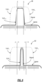
- FIGS. 9 and 10 are example plots of raised cosine functions for the TOF shapes.
- a FWHM of ⁇ 500 GHz and a range of ⁇ from -150 to -200 GHz would lead to a range of P from ⁇ 200 to ⁇ 100 GHz.
- An adjustable "insertion loss mismatch" factor is included but does not influence the net width of the transmission function, it results in an additional common mode insertion loss since the two TOFs are in series.
- the TOF can include any shaping such as a raised cosine shape and any order Gaussians.
- Discrete TOFs 12-1, 12-2 that are cascaded can add an additional 2-3dB of insertion loss to the Tx chain, however, with or without the EDFA, terminal circuit packs used for multiplexing contain high-Gain EDFA gain blocks capable of compensating for these losses. Thus, the insertion losses for these filters have a mild presence. Also, the TOFs 12-1, 12-2 can include single packaged devices with a single input- and output-fiber coupling points.
- FIG. 11 is a flowchart of a process for default bias calibration.
- FIG. 12 is a flowchart of a process for multi photodetector (PD) tuning.
- FIG. 13 is a flowchart of a process for single PD tuning.
- the cascaded TOF control system could be based on a total power measurement at the output PD, see FIGS. 5 and 6 .
- Each TOF voltage is biased until the filter edge approaches one side of the modulated spectrum, then finely back tuned.
- a calibration lookup table (LUT) of TOF center frequency versus TOF control voltage can be established. The LUT would be used to dead-reckon the TOFs to approximately the right center frequency, then a small bias voltage scan to get them optimized.
- LUT calibration lookup table
- Dynamic implementation of this control system allows the TOF system to adapt to the signal baud and actively suppress out band noise power as a function of transmission mode.
- Microelectromechanical systems (MEMS) TOFs are highly stable over temperature and ageing hence fixed voltage scans are very accurate.
- the PD between the two TOFs is an optional feature for accuracy though not a necessity for mission-mode control.
- Mission-mode optimization of the TOFs are controlled sequentially, based on total output power, the control diagrams for the various scenarios are shown in FIGS. 11, 12, and 13 .
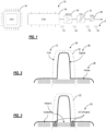
- FIG. 14 is a diagram of dense integration of cascaded TOFs 12-1, 12-2 and PDs 22 on an electro-optic (EO) printed circuit board (PCB) 100.
- the PDs 22 and TOFs 12-1, 12-2 can be localized on the PCB 100 or on an electro-optic (EO) daughter board within the PCB.
- the additional TOF and PD are positioned to minimize the impact on PCB layout/routing, fiber routing and to avoid design/placement changes to the existing components. Spacing the optical components away from the surface of the PCB allow for discrete components to be placed underneath to maximize PCB usable surface area. Again, discrete components is one embodiment, and the present disclosure contemplates an integrated solution as well.
- FIG. 15 is a graph of Example SNR penalties from wide TOF versus narrow/cascaded TOF configurations.
- FIG. 15 demonstrates how a probe's OSNR is affected as its nearest neighbors are separated in frequency.
- Square markers 150 represent current design operation (single wideband TOF design), while circles 152 indicate how TOF design implemented with bandwidth tunability (through this disclosure and its methodologies) improves the SNR ASE penalty by >3dB.
- Tx OSNR benefits of this magnitude can have significant (1-8%) capacity gains on subsea systems.
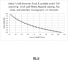
- FIG. 16 is a graph of the impact of fixed filter widths on signals with variable baud.
- the improvement in SNR assuming a fixed filter for an example modem, where the baud is tunable from 35-200GBd is shown in FIG. 16 .
- the system and method for a variable bandwidth TOF as described in this disclosure can provide over 7dB of improvement in the transmit OSNR. A significant benefit for next generation transponder technologies.
- FIG. 17 is a flowchart of a process 200 implemented in a coherent transmitter.
- the process 200 includes receiving an optical signal that was coherent modulated via a coherent modulator (step 201); and configuring a plurality of tunable optical filters, which are connected to an output of the coherent modulator, to create an effective transfer function having a variable width and center frequency based on the received optical signal (step 202).
- the process 200 can further include monitoring optical power via one or more photodetectors for the configuring of the plurality of tunable optical filters (step 203).
- Each of the plurality of tunable optical filters can include a fixed width and tunable center frequencies for the configuring.
- the effective transfer function can be based on setting of the tunable center frequencies.
- the present disclosure includes a process and apparatus that integrates a customizable tunable optical filter in coherent optical transmitters.
- the customizations can include but are not limited to, optical filter shaping, filter bandwidth tunability, filter frequency tunability, and adaptive optimizations of filter boundaries.
- Adaptive optimizations may include self-detection of the signal and noise extent to compress filter bandwidths appropriately for minimization of out of band noise power.
- the apparatus may be implemented through a composition of cascaded, sequential, or coupled tunable optical filters working in unison to achieve the customizations.
- the customizations and implementations can be managed by a control system based on dead reckoning of detected optical powers, via an intermediate photodetector and/or a single output photodetector.
- processors such as microprocessors; Central Processing Units (CPUs); Digital Signal Processors (DSPs): customized processors such as Network Processors (NPs) or Network Processing Units (NPUs), Graphics Processing Units (GPUs), or the like; Field-Programmable Gate Arrays (FPGAs); and the like along with unique stored program instructions (including both software and firmware) for control thereof to implement, in conjunction with certain non-processor circuits, some, most, or all of the functions of the methods and/or systems described herein.
- processors such as microprocessors; Central Processing Units (CPUs); Digital Signal Processors (DSPs): customized processors such as Network Processors (NPs) or Network Processing Units (NPUs), Graphics Processing Units (GPUs), or the like; Field-Programmable Gate Arrays (FPGAs); and the like along with unique stored program instructions (including both software and firmware) for control thereof to implement, in conjunction with certain non-processor circuits, some, most, or all
- circuitry configured to
- logic configured to
- some embodiments may include a non-transitory computer-readable medium having instructions stored thereon for programming a computer, server, appliance, device, at least one processor, circuit/circuitry, etc. to perform functions as described and claimed herein.
- Examples of such non-transitory computer-readable medium include, but are not limited to, a hard disk, an optical storage device, a magnetic storage device, a Read-Only Memory (ROM), a Programmable ROM (PROM), an Erasable PROM (EPROM), an Electrically EPROM (EEPROM), Flash memory, and the like.
- software can include instructions executable by one or more processors (e.g., any type of programmable circuitry or logic) that, in response to such execution, cause the one or more processors to perform a set of operations, steps, methods, processes, algorithms, functions, techniques, etc. as described herein for the various embodiments.
- processors e.g., any type of programmable circuitry or logic
Landscapes
- Engineering & Computer Science (AREA)
- Computer Networks & Wireless Communication (AREA)
- Signal Processing (AREA)
- Physics & Mathematics (AREA)
- Electromagnetism (AREA)
- Optical Communication System (AREA)
Description
- The present disclosure generally relates to optical networking. More particularly, the present disclosure relates to systems and methods for a bandwidth tunable optical filter (TOF) in coherent optical transmitters.
- The transmit optical signal-to-noise ratio (OSNR) from any network element (NE) terminal can be a significant factor for network operators who set high performance standards for colorless configurations, particularly in submarine line terminal equipment (SLTE) to achieve the highest spectrally efficient transmission mode from the transmitter, transceiver, transponder, modem, etc. (of note, all of these include an optical transmitter, and are contemplated herein). Terminal OSNR penalties include line amplifier noise figure contributions, inter-channel crosstalk, and noise funneling from colorless multiplexer structures. Noise funneling refers to noise being added when multiple signals are multiplexed together via multiplexer structures. For example, noise pedestals outside the signal bandwidth of one signal can contribute to noise in another signal.
For the noise funneling, current modem optical filtering schemes include a TOF in the transmitter having a tunable center frequency but a static bandwidth (full width at half maximum (FWHM)). A static bandwidth filter provides some benefit to the noise funneling, namely filtering out of band spectrum, and its center frequency can be optimized, but such filters are not bandwidth tunable, in terms of the passband, in the optical domain. The inventors are aware of no known prior solutions for tunable bandwidth filtering of an optical signal in a coherent transmitter.US 2003/133650 A1 describes a system and method for transmitting optical signals using IIR and FIR filtration.US 2016/226616 A1 describes a wavelength/bandwidth tunable optical filter and driving method.US 2004/131309 A1 describes a tunable optical filter, optical switch and optical add/crop multiplexer. WANG TAI-CHUN ET AL, 2020 CONFERENCE ON LASERS AND ELECTRO-OPTICAS (CLEOR) OSA, 10 May 2020 (2020-05-10), pages 1-2, XP033822698 describes "Bandwidth and wavelength tunable optical filter based on cascaded waveguide grating on silicon-on-insulator". LIU ET. IEEE PHOTONICS JOURNAL, IEEE, USA, vol 11. No1. 1 February 2019 (2019-02-01) pages 1-10, XP011709122, DOI: 10.1109/JPHOT.2019.2896257 describes "Bandwidth and wavelength tunable all-optical filter based on cascaded opto-mechanical mirroring resonators." - The present disclosure relates to systems and methods for a bandwidth tunable optical filter (TOF) in coherent optical transmitters. In particular, the present disclosure includes TOFs on a transmitter that provides tunable bandwidth filtering in the optical domain. The TOFs are cascaded and can be included in discrete form on electro-optic printed circuit boards (PCBs), or integrated in various electro-optic material systems such as in silicon photonics, photonic integrated circuits (PICs), as well as hybrid and other approaches. The advantage of this approach includes improved OSNR in colorless transmitters.
- The invention concerns a coherent optical transmitter according to
claim 1, including a coherent modulator; and a plurality of tunable optical filters connected to an output of the coherent modulator, wherein the plurality of tunable optical filters are configurable to create an effective transfer function having a variable width and center frequency. The plurality of tunable optical filters are cascaded with one another. The plurality of tunable optical filters are integrated within the coherent optical transmitter. The coherent optical transmitter further includes the coherent modulator. The coherent optical transmitter can further include an optical amplifier located between the coherent modulator and the plurality of tunable optical filters. - Each of the plurality of tunable optical filters can include a fixed width and tunable center frequencies. The effective transfer function can be based on setting of the tunable center frequencies. A passband of the effective transfer function can be based on frequency offsets and Full Width at Half Maximum (FWHM) of the plurality of tunable optical filters. One or more of the plurality of tunable optical filters can have a shape that includes any of a raised cosine shape and any order Gaussians. One or more of the plurality of tunable optical filters can be based on Microelectromechanical systems (MEMS).
- The coherent optical transmitter can further include one or more photodetectors for monitoring and configuration of the plurality of tunable optical filters. The one or more photodetectors can include a photodetector between the plurality of tunable optical filters. The plurality of tunable optical filters can be controlled based on total output power. The plurality of tunable optical filters can be controlled sequentially. The plurality of tunable optical filters can be configured based on spectral width of an output signal from the coherent modulator.
- The invention further concerns a method according to independent claim 13 and implemented in a coherent transmitter, including steps of receiving an optical signal that was coherent modulated via a coherent modulator; and configuring a plurality of tunable optical filters, which are connected to an output of the coherent modulator, to create an effective transfer function having a variable width and center frequency based on the received optical signal.
- The steps can include monitoring optical power via one or more photodetectors for the configuring of the plurality of tunable optical filters. Each of the plurality of tunable optical filters can include a fixed width and tunable center frequencies. The effective transfer function can be based on setting the tunable center frequencies. The steps can include amplifying a signal from the coherent modulator before, in between, or after any of the plurality of tunable optical filters.
- The present disclosure is illustrated and described herein with reference to the various drawings, in which like reference numbers are used to denote like system components/method steps, as appropriate, and in which:
-
FIG. 1 is a block diagram of example components in a coherent transmitter with a single TOF. -
FIG. 2 is a spectral diagram of a single channel having signal components and noise components and filtered by the TOF. -
FIG. 3 is a spectral diagram of the single channel illustrating noise pedestals located inband of the TOF and contributing to noise funneling. -
FIG. 4 is a diagram illustrating three example optical signals λ1, λ2, λ3 being multiplexed by a multiplexer to illustrate noise funneling. -
FIG. 5 is a block diagram of example components in a coherent transmitter with a dual TOF. -
FIG. 6 is a block diagram of example components in a coherent transmitter with a dual TOF in an amp-less configuration. -
FIG. 7 are spectral diagrams illustrating two filter responses from the TOFs and an effective third filter response based on the center frequencies of the TOFs. -
FIG. 8 are plots of signals where TOF1 and TOF2 are centered on frequencies f1 and f2 respectively, and where the TOFs are offset by a delta. -
FIGS. 9 and 10 are example plots of raised cosine functions for the TOF shapes. -
FIG. 11 is a flowchart of a process for default bias calibration. -
FIG. 12 is a flowchart of a process for multi photodetector (PD) tuning. -
FIG. 13 is a flowchart of a process for single PD tuning. -
FIG. 14 is a diagram of dense integration of cascaded TOFs and PDs on an electro-optic (EO) printed circuit board (PCB). -
FIG. 15 is a graph of Example SNR penalties from wide TOF versus narrow/cascaded TOF configurations. -
FIG. 16 is a graph of the impact of fixed filter widths on signals with variable baud. -
FIG. 17 is a flowchart of a process implemented in a coherent transmitter. - Again, the present disclosure relates to systems and methods for a bandwidth tunable optical filter (TOF) in coherent optical transmitters. In particular, the present disclosure includes TOFs on a transmitter that provides tunable bandwidth filtering in the optical domain. The TOFs are cascaded and can be included in discrete form on electro-optic printed circuit boards (PCBs), or integrated in various electro-optic material systems such as in silicon photonics, photonic integrated circuits (PICs), as well as hybrid and other approaches. The advantage of this approach includes improved OSNR in colorless transmitters.
-
FIG. 1 is a block diagram of example components in a coherentoptical transmitter 10 with asingle TOF 12. In this example, there is an application specific integrated circuit (ASIC) 14 that is configured to provided digital functions, including digital signal processing (DSP) functions. A coherent driver modulator (CDM) 16 interfaces theASIC 14 and is configured to provide an coherently modulated optical signal output which is amplified by anamplifier 18, such as an erbium doped fiber amplifier (EDFA), and which is filtered by theTOF 12 and potentially attenuated via a variable optical attenuator (VOA) 20. Further, there can be various photodetectors (PD) 22 along thetransmitter 10 for monitoring power levels, such as via taps. - Those skilled in the art will recognize a practical embodiment of the
coherent transmitter 10 can include various other components which are omitted for simplicity. Also, of note,FIG. 1 is shown with discrete components for example only. Those skilled in the art will recognize these various functional components can be realized in an integrated manner, such as in silicon photonics, photonic integrated circuits (PICs), as well as hybrid and other approaches. - Again, terminal OSNR penalties are composed from line amp noise figure contributions, inter-channel crosstalk, and noise funneling from colorless mux structures. The latter penalty is reduced using the
TOF 12 on the front end of a coherent transmitter as shown inFIG. 2 . ThisTOF 12 is controlled and centered based on the photodetectors (PD) readings pre- andpost-TOF 12. -
FIG. 2 is a spectral diagram of asingle channel 24 havingsignal components 26 andnoise components 28 and filtered by theTOF 12.FIG. 3 is a spectral diagram of thesingle channel 24 illustrating noise pedestals 30 located inband of theTOF 12 and contributing to noise funneling. TheTOF 12 is center frequency tunable, meaning afilter shape 32 can be moved, but the overall shape and optical bandwidth is fixed. - In variable- or tunable-baud modems, as the signal gets narrower, the total inband noise power increases, because the
TOF 12 bandwidth is fixed, thereby diminishing the transmit OSNR further after colorless multiplexing.FIG. 4 is a diagram illustrating three example optical signals λ1, λ2, λ3 being multiplexed by amultiplexer 40 to illustrate noise funneling. The primary shortcoming of the fixedbandwidth TOF 12 is the increased noise penalty due to noise funneling.FIG. 4 illustrates the increased inter-channel noise power after colorless multiplexing due to the extended bandwidth of the TOF used. This noise penalty increases as the signal baud is reduced (since the TOF bandwidth remains the same). - The present disclosure includes a bandwidth tunable TOF system that minimizes noise funneling penalties in tunable baud modems. The filter design, centering, control, and layout are described herein.
-
FIG. 5 is a block diagram of example components in acoherent transmitter 10 with a dual TOF 12-1, 12-2.FIG. 6 is a block diagram of example components in acoherent transmitter 10 with a dual TOF 12-1, 12-2 in an amp-less configuration. These are two example configurations and those skilled in the art will recognize there can be other embodiments as well as more than two TOFs. - The present disclosures utilizes multiple fixed bandwidth TOFs 12-1, 12-2 that are cascaded with their center frequencies offset from each other. The offset allows the two fixed TOFs 12-1, 12-2 to effectively produce a third filter response, where the bandwidth is dictated by the center frequency offset.
FIG. 7 are spectral diagrams illustrating two filter responses from the TOFs 12-1, 12-2 and an effectivethird filter response 50 based on the center frequencies of the TOFs 12-1, 12-2. Of note, the filter responses of each of the TOFs 12-1, 12-2 have a fixed width, but this can lead to a variable width based on the center frequencies of the TOFs 12-1, 12-2. For example, spreading the center frequencies apart reduces the bandwidth of thefilter response 50 whereas bring the center frequencies together increases the bandwidth of thefilter response 50, up to the fixed width (or the smaller width) of the TOFs 12-1, 12-2. Also, the solution need not be limited to two TOFs; however, the primary function of bandwidth tunability is easily achieved with a dual TOF configuration. - The effective transfer function created by the cascaded TOFs are a bandpass filter where the width is dictated by the frequency offset of TOF1 and TOF2.
FIG. 8 illustrates awideband signal 60 where TOF1 and TOF2 are centered on frequencies f1 and f2 respectively, f1 and f2 are appropriately chosen by a control loop (described below) to minimize the amount of InTOFband noise, minimizing noise funneling. Anarrower signal 62 is the same signal reduced in baud, where f1 and f2 are detuned by an offset (Δ) determined by the control loop to narrow the effective bandpass filter and suppress outband noise further. - The tunable bandwidth aspect of the cascaded TOF 12-1, 12-2 is achieved by differential frequency offset control of the two TOFs 12-1, 12-2 relative to one another. For high-Q cascaded filters, the flat passband width (P) of the net transmission spectrum is approximately: P = -2δ + FWHM, assuming each of the two TOFs 12-1, 12-2 has the same Full Width at Half Maximum (FWHM), and each TOF is offset by plus or minus δ relative to one another. δ is the passband width of each of the two TOFs 12-1, 12-2.
-
FIGS. 9 and 10 are example plots of raised cosine functions for the TOF shapes. For example signals, with reasonable assumptions for the filter shapes and widths, a FWHM of ~500 GHz and a range of δ from -150 to -200 GHz would lead to a range of P from ~200 to ≲ 100 GHz. An adjustable "insertion loss mismatch" factor is included but does not influence the net width of the transmission function, it results in an additional common mode insertion loss since the two TOFs are in series. Of course, the TOF can include any shaping such as a raised cosine shape and any order Gaussians. - Discrete TOFs 12-1, 12-2 that are cascaded can add an additional 2-3dB of insertion loss to the Tx chain, however, with or without the EDFA, terminal circuit packs used for multiplexing contain high-Gain EDFA gain blocks capable of compensating for these losses. Thus, the insertion losses for these filters have a mild presence. Also, the TOFs 12-1, 12-2 can include single packaged devices with a single input- and output-fiber coupling points.
-
FIG. 11 is a flowchart of a process for default bias calibration.FIG. 12 is a flowchart of a process for multi photodetector (PD) tuning.FIG. 13 is a flowchart of a process for single PD tuning. The cascaded TOF control system could be based on a total power measurement at the output PD, seeFIGS. 5 and 6 . Each TOF voltage is biased until the filter edge approaches one side of the modulated spectrum, then finely back tuned. A calibration lookup table (LUT) of TOF center frequency versus TOF control voltage can be established. The LUT would be used to dead-reckon the TOFs to approximately the right center frequency, then a small bias voltage scan to get them optimized. Dynamic implementation of this control system allows the TOF system to adapt to the signal baud and actively suppress out band noise power as a function of transmission mode. Microelectromechanical systems (MEMS) TOFs are highly stable over temperature and ageing hence fixed voltage scans are very accurate. The PD between the two TOFs is an optional feature for accuracy though not a necessity for mission-mode control. Mission-mode optimization of the TOFs are controlled sequentially, based on total output power, the control diagrams for the various scenarios are shown inFIGS. 11, 12, and 13 . -
FIG. 14 is a diagram of dense integration of cascaded TOFs 12-1, 12-2 and PDs 22 on an electro-optic (EO) printed circuit board (PCB) 100. The PDs 22 and TOFs 12-1, 12-2 can be localized on thePCB 100 or on an electro-optic (EO) daughter board within the PCB. The additional TOF and PD are positioned to minimize the impact on PCB layout/routing, fiber routing and to avoid design/placement changes to the existing components. Spacing the optical components away from the surface of the PCB allow for discrete components to be placed underneath to maximize PCB usable surface area. Again, discrete components is one embodiment, and the present disclosure contemplates an integrated solution as well. - Improved OSNR on colorless Tx terminals is the primary performance benefit in the present disclosure.
FIG. 15 is a graph of Example SNR penalties from wide TOF versus narrow/cascaded TOF configurations.FIG. 15 demonstrates how a probe's OSNR is affected as its nearest neighbors are separated in frequency.Square markers 150 represent current design operation (single wideband TOF design), whilecircles 152 indicate how TOF design implemented with bandwidth tunability (through this disclosure and its methodologies) improves the SNRASE penalty by >3dB. Tx OSNR benefits of this magnitude can have significant (1-8%) capacity gains on subsea systems. -
FIG. 16 is a graph of the impact of fixed filter widths on signals with variable baud. Alternatively, the improvement in SNR assuming a fixed filter for an example modem, where the baud is tunable from 35-200GBd is shown inFIG. 16 . The system and method for a variable bandwidth TOF as described in this disclosure can provide over 7dB of improvement in the transmit OSNR. A significant benefit for next generation transponder technologies. -
FIG. 17 is a flowchart of aprocess 200 implemented in a coherent transmitter. Theprocess 200 includes receiving an optical signal that was coherent modulated via a coherent modulator (step 201); and configuring a plurality of tunable optical filters, which are connected to an output of the coherent modulator, to create an effective transfer function having a variable width and center frequency based on the received optical signal (step 202). - The
process 200 can further include monitoring optical power via one or more photodetectors for the configuring of the plurality of tunable optical filters (step 203). Each of the plurality of tunable optical filters can include a fixed width and tunable center frequencies for the configuring. The effective transfer function can be based on setting of the tunable center frequencies. - The present disclosure includes a process and apparatus that integrates a customizable tunable optical filter in coherent optical transmitters. The customizations can include but are not limited to, optical filter shaping, filter bandwidth tunability, filter frequency tunability, and adaptive optimizations of filter boundaries. Adaptive optimizations may include self-detection of the signal and noise extent to compress filter bandwidths appropriately for minimization of out of band noise power. The apparatus may be implemented through a composition of cascaded, sequential, or coupled tunable optical filters working in unison to achieve the customizations.
- The customizations and implementations can be managed by a control system based on dead reckoning of detected optical powers, via an intermediate photodetector and/or a single output photodetector.
- It will be appreciated that some embodiments described herein may include or utilize one or more generic or specialized processors ("one or more processors") such as microprocessors; Central Processing Units (CPUs); Digital Signal Processors (DSPs): customized processors such as Network Processors (NPs) or Network Processing Units (NPUs), Graphics Processing Units (GPUs), or the like; Field-Programmable Gate Arrays (FPGAs); and the like along with unique stored program instructions (including both software and firmware) for control thereof to implement, in conjunction with certain non-processor circuits, some, most, or all of the functions of the methods and/or systems described herein. Alternatively, some or all functions may be implemented by a state machine that has no stored program instructions, or in one or more Application-Specific Integrated Circuits (ASICs), in which each function or some combinations of certain of the functions are implemented as custom logic or circuitry. Of course, a combination of the aforementioned approaches may be used. For some of the embodiments described herein, a corresponding device in hardware and optionally with software, firmware, and a combination thereof can be referred to as "circuitry configured to," "logic configured to," etc. perform a set of operations, steps, methods, processes, algorithms, functions, techniques, etc. on digital and/or analog signals as described herein for the various embodiments.
- Moreover, some embodiments may include a non-transitory computer-readable medium having instructions stored thereon for programming a computer, server, appliance, device, at least one processor, circuit/circuitry, etc. to perform functions as described and claimed herein. Examples of such non-transitory computer-readable medium include, but are not limited to, a hard disk, an optical storage device, a magnetic storage device, a Read-Only Memory (ROM), a Programmable ROM (PROM), an Erasable PROM (EPROM), an Electrically EPROM (EEPROM), Flash memory, and the like. When stored in the non-transitory computer-readable medium, software can include instructions executable by one or more processors (e.g., any type of programmable circuitry or logic) that, in response to such execution, cause the one or more processors to perform a set of operations, steps, methods, processes, algorithms, functions, techniques, etc. as described herein for the various embodiments.
- The scope of protection of the present invention is in any case understood as being defined by the appended claims.
Claims (13)
- A coherent optical transmitter (10) comprising:a coherent driver modulator (16);a plurality of tunable optical filters (12), integrated within the coherent optical transmitter (10) and connected such that the plurality of tunable optical filters (12) are cascaded relative to one another, connected to an output of the coherent driver modulator (16), wherein the plurality of tunable optical filters (12) are configurable to create an effective transfer function having a variable width and center frequency; andone or more photodetectors (22) configured to monitor the plurality of tunable optical filters (12), wherein the plurality of tunable optical filters (12) are configured based on signal baud of a signal from the output determined based on measurements from the one or more photodetectors (22).
- The coherent optical transmitter (10) as claimed in claim 1, wherein the plurality of tunable optical filters are configured together as an integrated device formed using silicon photonics.
- The coherent optical transmitter (10) as claimed in claim 2, wherein the integrated device further includes the coherent driver modulator (16).
- The coherent optical transmitter (10) as claimed in any one of claims 1 to 3, further comprising an optical amplifier (18) located between the coherent driver modulator (16) and the plurality of tunable optical filters (12).
- The coherent optical transmitter (10) as claimed in any one of claims 1 to 4, wherein each of the plurality of tunable optical filters (12) includes a fixed width and tunable center frequencies.
- The coherent optical transmitter (10) as claimed in claim 5, wherein the effective transfer function is based on setting of the tunable center frequencies.
- The coherent optical transmitter (10) as claimed in any one of claims 1 to 5, wherein a passband of the effective transfer function is based on frequency offsets and Full Width at Half Maximum (FWHM) of the plurality of tunable optical filters (12).
- The coherent optical transmitter (10) as claimed in any one of claims 1 to 7, wherein one or more of the plurality of tunable optical filters (12) has a shape that includes any of a raised cosine shape and any order Gaussians.
- The coherent optical transmitter (10) as claimed in any one of claims 1 to 8, wherein one or more of the plurality of tunable optical filters (10) are based on Microelectromechanical systems (MEMS).
- The coherent optical transmitter (10) as claimed in any one of claims 1 to 9, wherein the plurality of tunable optical filters (12) are further configured based on total output power.
- The coherent optical transmitter (10) as claimed in any one of claims 1 to 9, further comprising means for sequentially tuning the plurality of tunable filters (12) so that the voltage of each filter is biased until the filter edge approaches one side of the modulated spectrum and then finely back tuned.
- The coherent optical transmitter (10) as claimed in any one of claims 1 to 9, wherein the plurality of tunable optical filters (12) are configured based on spectral width of an output signal from the coherent driver modulator (16).
- A method (200) implemented in a coherent optical transmitter (10) comprising steps of:receiving (201) an optical signal that was coherent modulated via a coherent driver modulator (16);measuring a signal baud of the optical signal via one or more photodetectors (220: andconfiguring (202) a plurality of tunable optical filters (12), integrated within the coherent optical transmitter (10) and connected such that the plurality of tunable optical filters (12) are cascaded relative to one another, which are connected to an output of the coherent driver modulator (16), to create an effective transfer function having a variable width and center frequency based on the signal baud of the received optical signal.
Applications Claiming Priority (2)
| Application Number | Priority Date | Filing Date | Title |
|---|---|---|---|
| US17/712,263 US12463727B2 (en) | 2022-04-04 | 2022-04-04 | Tunable optical filter in coherent optical transmitters |
| PCT/US2023/017399 WO2023196293A1 (en) | 2022-04-04 | 2023-04-04 | Tunable optical filter in coherent optical transmitters |
Publications (2)
| Publication Number | Publication Date |
|---|---|
| EP4282092A1 EP4282092A1 (en) | 2023-11-29 |
| EP4282092B1 true EP4282092B1 (en) | 2024-04-24 |
Family
ID=88206807
Family Applications (1)
| Application Number | Title | Priority Date | Filing Date |
|---|---|---|---|
| EP23721092.7A Active EP4282092B1 (en) | 2022-04-04 | 2023-04-04 | Tunable optical filter in coherent optical transmitters |
Country Status (3)
| Country | Link |
|---|---|
| EP (1) | EP4282092B1 (en) |
| CN (1) | CN117178501A (en) |
| CA (1) | CA3210061A1 (en) |
Family Cites Families (6)
| Publication number | Priority date | Publication date | Assignee | Title |
|---|---|---|---|---|
| FR2787262A1 (en) * | 1998-12-14 | 2000-06-16 | Cit Alcatel | FIBER OPTIC TRANSMISSION SYSTEM WITH VARIABLE WIDTH RECEIVING FILTER |
| JP4047004B2 (en) * | 2001-12-28 | 2008-02-13 | 富士通株式会社 | Method and apparatus for controlling optical wavelength tunable filter |
| US20030133650A1 (en) * | 2002-01-16 | 2003-07-17 | Farhad Hakimi | System and method of transmitting optical signals using IIR and FIR filtration |
| US20040131309A1 (en) * | 2002-09-03 | 2004-07-08 | Xinxiong Zhang | Tunable optical filter, optical switch, and optical add/drop multiplexer employing linearly variable thin film optical filters |
| KR20160095684A (en) * | 2015-02-03 | 2016-08-12 | 한국전자통신연구원 | Wavelength/Bandwidth Tunable Optical Filter and Driving Method Thereof |
| US10277352B2 (en) * | 2016-05-24 | 2019-04-30 | Ciena Corporation | Noise suppression and amplification systems and methods for colorless optical add/drop devices |
-
2023
- 2023-04-04 CA CA3210061A patent/CA3210061A1/en active Pending
- 2023-04-04 CN CN202380010917.7A patent/CN117178501A/en active Pending
- 2023-04-04 EP EP23721092.7A patent/EP4282092B1/en active Active
Also Published As
| Publication number | Publication date |
|---|---|
| EP4282092A1 (en) | 2023-11-29 |
| CN117178501A (en) | 2023-12-05 |
| CA3210061A1 (en) | 2023-10-04 |
Similar Documents
| Publication | Publication Date | Title |
|---|---|---|
| US6396051B1 (en) | High resolution optical performance monitor for DWDM system | |
| US8687982B2 (en) | OSNR measuring device and optical communication system | |
| US7142785B2 (en) | Light branching/inserting apparatus and light branching apparatus using wavelength selection filter | |
| JP4626918B2 (en) | Raman optical repeater | |
| JPWO2008105202A1 (en) | Optical fiber transmission device and optical communication network | |
| CN102870351B (en) | Method and device for inhibiting pilot signal crosstalk, and pilot signal receiving apparatus | |
| US20110081146A1 (en) | Optical monitor device | |
| JP3969807B2 (en) | Dispersion compensation device | |
| JP2010535006A (en) | System and method for wavelength monitoring and wavelength control | |
| JPH09191303A (en) | Optical transmission path | |
| US6674773B1 (en) | Multi-wavelength Raman laser | |
| US6421167B1 (en) | Multiple function bandwidth management systems | |
| JP2002296629A (en) | Method for converting wavelength using optical four wave mixing and considering noise, wavelength converter and light source | |
| JP2023180636A (en) | Optical communication device, optical communication system, and optical power control method | |
| JP4553609B2 (en) | Optical transmission system with noise removal function | |
| JP3879802B2 (en) | Setting method of signal light wavelength of optical transmission system | |
| JP2001044970A (en) | Wavelength multiplex transmitting device | |
| US7474854B2 (en) | Optical transmission system | |
| US12463727B2 (en) | Tunable optical filter in coherent optical transmitters | |
| CA3210061A1 (en) | Tunable optical filter in coherent optical transmitters | |
| JP2014229913A (en) | Wdm signal optical repeating device, method and system | |
| WO2021060124A1 (en) | Optical communication system, optical communication device, optical communication method, and storage medium | |
| JP2000312185A (en) | Optical repeating amplifier for wavelength multiplex optical transmission, and wavelength multiplex optical transmission device using the same | |
| KR100278440B1 (en) | Channel monitoring device of wavelength division multiple system | |
| EP3289704B1 (en) | Optical receiver and method of receiving an optical communications signal |
Legal Events
| Date | Code | Title | Description |
|---|---|---|---|
| STAA | Information on the status of an ep patent application or granted ep patent |
Free format text: STATUS: UNKNOWN |
|
| STAA | Information on the status of an ep patent application or granted ep patent |
Free format text: STATUS: THE INTERNATIONAL PUBLICATION HAS BEEN MADE |
|
| PUAI | Public reference made under article 153(3) epc to a published international application that has entered the european phase |
Free format text: ORIGINAL CODE: 0009012 |
|
| STAA | Information on the status of an ep patent application or granted ep patent |
Free format text: STATUS: REQUEST FOR EXAMINATION WAS MADE |
|
| 17P | Request for examination filed |
Effective date: 20230821 |
|
| AK | Designated contracting states |
Kind code of ref document: A1 Designated state(s): AL AT BE BG CH CY CZ DE DK EE ES FI FR GB GR HR HU IE IS IT LI LT LU LV MC ME MK MT NL NO PL PT RO RS SE SI SK SM TR |
|
| STAA | Information on the status of an ep patent application or granted ep patent |
Free format text: STATUS: EXAMINATION IS IN PROGRESS |
|
| 17Q | First examination report despatched |
Effective date: 20231206 |
|
| P01 | Opt-out of the competence of the unified patent court (upc) registered |
Effective date: 20240108 |
|
| GRAP | Despatch of communication of intention to grant a patent |
Free format text: ORIGINAL CODE: EPIDOSNIGR1 |
|
| STAA | Information on the status of an ep patent application or granted ep patent |
Free format text: STATUS: GRANT OF PATENT IS INTENDED |
|
| GRAS | Grant fee paid |
Free format text: ORIGINAL CODE: EPIDOSNIGR3 |
|
| INTG | Intention to grant announced |
Effective date: 20240223 |
|
| GRAA | (expected) grant |
Free format text: ORIGINAL CODE: 0009210 |
|
| STAA | Information on the status of an ep patent application or granted ep patent |
Free format text: STATUS: THE PATENT HAS BEEN GRANTED |
|
| DAV | Request for validation of the european patent (deleted) | ||
| DAX | Request for extension of the european patent (deleted) | ||
| AK | Designated contracting states |
Kind code of ref document: B1 Designated state(s): AL AT BE BG CH CY CZ DE DK EE ES FI FR GB GR HR HU IE IS IT LI LT LU LV MC ME MK MT NL NO PL PT RO RS SE SI SK SM TR |
|
| REG | Reference to a national code |
Ref country code: GB Ref legal event code: FG4D |
|
| REG | Reference to a national code |
Ref country code: CH Ref legal event code: EP |
|
| REG | Reference to a national code |
Ref country code: DE Ref legal event code: R096 Ref document number: 602023000066 Country of ref document: DE |
|
| REG | Reference to a national code |
Ref country code: IE Ref legal event code: FG4D |
|
| REG | Reference to a national code |
Ref country code: NL Ref legal event code: FP |
|
| REG | Reference to a national code |
Ref country code: LT Ref legal event code: MG9D |
|
| REG | Reference to a national code |
Ref country code: AT Ref legal event code: MK05 Ref document number: 1680738 Country of ref document: AT Kind code of ref document: T Effective date: 20240424 |
|
| PG25 | Lapsed in a contracting state [announced via postgrant information from national office to epo] |
Ref country code: IS Free format text: LAPSE BECAUSE OF FAILURE TO SUBMIT A TRANSLATION OF THE DESCRIPTION OR TO PAY THE FEE WITHIN THE PRESCRIBED TIME-LIMIT Effective date: 20240824 |
|
| PG25 | Lapsed in a contracting state [announced via postgrant information from national office to epo] |
Ref country code: BG Free format text: LAPSE BECAUSE OF FAILURE TO SUBMIT A TRANSLATION OF THE DESCRIPTION OR TO PAY THE FEE WITHIN THE PRESCRIBED TIME-LIMIT Effective date: 20240424 |
|
| PG25 | Lapsed in a contracting state [announced via postgrant information from national office to epo] |
Ref country code: FI Free format text: LAPSE BECAUSE OF FAILURE TO SUBMIT A TRANSLATION OF THE DESCRIPTION OR TO PAY THE FEE WITHIN THE PRESCRIBED TIME-LIMIT Effective date: 20240424 Ref country code: HR Free format text: LAPSE BECAUSE OF FAILURE TO SUBMIT A TRANSLATION OF THE DESCRIPTION OR TO PAY THE FEE WITHIN THE PRESCRIBED TIME-LIMIT Effective date: 20240424 |
|
| PG25 | Lapsed in a contracting state [announced via postgrant information from national office to epo] |
Ref country code: GR Free format text: LAPSE BECAUSE OF FAILURE TO SUBMIT A TRANSLATION OF THE DESCRIPTION OR TO PAY THE FEE WITHIN THE PRESCRIBED TIME-LIMIT Effective date: 20240725 |
|
| PG25 | Lapsed in a contracting state [announced via postgrant information from national office to epo] |
Ref country code: PT Free format text: LAPSE BECAUSE OF FAILURE TO SUBMIT A TRANSLATION OF THE DESCRIPTION OR TO PAY THE FEE WITHIN THE PRESCRIBED TIME-LIMIT Effective date: 20240826 |
|
| PG25 | Lapsed in a contracting state [announced via postgrant information from national office to epo] |
Ref country code: ES Free format text: LAPSE BECAUSE OF FAILURE TO SUBMIT A TRANSLATION OF THE DESCRIPTION OR TO PAY THE FEE WITHIN THE PRESCRIBED TIME-LIMIT Effective date: 20240424 |
|
| PG25 | Lapsed in a contracting state [announced via postgrant information from national office to epo] |
Ref country code: AT Free format text: LAPSE BECAUSE OF FAILURE TO SUBMIT A TRANSLATION OF THE DESCRIPTION OR TO PAY THE FEE WITHIN THE PRESCRIBED TIME-LIMIT Effective date: 20240424 |
|
| PG25 | Lapsed in a contracting state [announced via postgrant information from national office to epo] |
Ref country code: PL Free format text: LAPSE BECAUSE OF FAILURE TO SUBMIT A TRANSLATION OF THE DESCRIPTION OR TO PAY THE FEE WITHIN THE PRESCRIBED TIME-LIMIT Effective date: 20240424 |
|
| PG25 | Lapsed in a contracting state [announced via postgrant information from national office to epo] |
Ref country code: LV Free format text: LAPSE BECAUSE OF FAILURE TO SUBMIT A TRANSLATION OF THE DESCRIPTION OR TO PAY THE FEE WITHIN THE PRESCRIBED TIME-LIMIT Effective date: 20240424 |
|
| PG25 | Lapsed in a contracting state [announced via postgrant information from national office to epo] |
Ref country code: PT Free format text: LAPSE BECAUSE OF FAILURE TO SUBMIT A TRANSLATION OF THE DESCRIPTION OR TO PAY THE FEE WITHIN THE PRESCRIBED TIME-LIMIT Effective date: 20240826 Ref country code: PL Free format text: LAPSE BECAUSE OF FAILURE TO SUBMIT A TRANSLATION OF THE DESCRIPTION OR TO PAY THE FEE WITHIN THE PRESCRIBED TIME-LIMIT Effective date: 20240424 Ref country code: NO Free format text: LAPSE BECAUSE OF FAILURE TO SUBMIT A TRANSLATION OF THE DESCRIPTION OR TO PAY THE FEE WITHIN THE PRESCRIBED TIME-LIMIT Effective date: 20240724 Ref country code: LV Free format text: LAPSE BECAUSE OF FAILURE TO SUBMIT A TRANSLATION OF THE DESCRIPTION OR TO PAY THE FEE WITHIN THE PRESCRIBED TIME-LIMIT Effective date: 20240424 Ref country code: IS Free format text: LAPSE BECAUSE OF FAILURE TO SUBMIT A TRANSLATION OF THE DESCRIPTION OR TO PAY THE FEE WITHIN THE PRESCRIBED TIME-LIMIT Effective date: 20240824 Ref country code: HR Free format text: LAPSE BECAUSE OF FAILURE TO SUBMIT A TRANSLATION OF THE DESCRIPTION OR TO PAY THE FEE WITHIN THE PRESCRIBED TIME-LIMIT Effective date: 20240424 Ref country code: GR Free format text: LAPSE BECAUSE OF FAILURE TO SUBMIT A TRANSLATION OF THE DESCRIPTION OR TO PAY THE FEE WITHIN THE PRESCRIBED TIME-LIMIT Effective date: 20240725 Ref country code: FI Free format text: LAPSE BECAUSE OF FAILURE TO SUBMIT A TRANSLATION OF THE DESCRIPTION OR TO PAY THE FEE WITHIN THE PRESCRIBED TIME-LIMIT Effective date: 20240424 Ref country code: ES Free format text: LAPSE BECAUSE OF FAILURE TO SUBMIT A TRANSLATION OF THE DESCRIPTION OR TO PAY THE FEE WITHIN THE PRESCRIBED TIME-LIMIT Effective date: 20240424 Ref country code: BG Free format text: LAPSE BECAUSE OF FAILURE TO SUBMIT A TRANSLATION OF THE DESCRIPTION OR TO PAY THE FEE WITHIN THE PRESCRIBED TIME-LIMIT Effective date: 20240424 Ref country code: AT Free format text: LAPSE BECAUSE OF FAILURE TO SUBMIT A TRANSLATION OF THE DESCRIPTION OR TO PAY THE FEE WITHIN THE PRESCRIBED TIME-LIMIT Effective date: 20240424 Ref country code: RS Free format text: LAPSE BECAUSE OF FAILURE TO SUBMIT A TRANSLATION OF THE DESCRIPTION OR TO PAY THE FEE WITHIN THE PRESCRIBED TIME-LIMIT Effective date: 20240724 |
|
| PG25 | Lapsed in a contracting state [announced via postgrant information from national office to epo] |
Ref country code: DK Free format text: LAPSE BECAUSE OF FAILURE TO SUBMIT A TRANSLATION OF THE DESCRIPTION OR TO PAY THE FEE WITHIN THE PRESCRIBED TIME-LIMIT Effective date: 20240424 |
|
| PG25 | Lapsed in a contracting state [announced via postgrant information from national office to epo] |
Ref country code: EE Free format text: LAPSE BECAUSE OF FAILURE TO SUBMIT A TRANSLATION OF THE DESCRIPTION OR TO PAY THE FEE WITHIN THE PRESCRIBED TIME-LIMIT Effective date: 20240424 |
|
| PG25 | Lapsed in a contracting state [announced via postgrant information from national office to epo] |
Ref country code: CZ Free format text: LAPSE BECAUSE OF FAILURE TO SUBMIT A TRANSLATION OF THE DESCRIPTION OR TO PAY THE FEE WITHIN THE PRESCRIBED TIME-LIMIT Effective date: 20240424 |
|
| PG25 | Lapsed in a contracting state [announced via postgrant information from national office to epo] |
Ref country code: SK Free format text: LAPSE BECAUSE OF FAILURE TO SUBMIT A TRANSLATION OF THE DESCRIPTION OR TO PAY THE FEE WITHIN THE PRESCRIBED TIME-LIMIT Effective date: 20240424 Ref country code: RO Free format text: LAPSE BECAUSE OF FAILURE TO SUBMIT A TRANSLATION OF THE DESCRIPTION OR TO PAY THE FEE WITHIN THE PRESCRIBED TIME-LIMIT Effective date: 20240424 |
|
| REG | Reference to a national code |
Ref country code: DE Ref legal event code: R097 Ref document number: 602023000066 Country of ref document: DE |
|
| PG25 | Lapsed in a contracting state [announced via postgrant information from national office to epo] |
Ref country code: SM Free format text: LAPSE BECAUSE OF FAILURE TO SUBMIT A TRANSLATION OF THE DESCRIPTION OR TO PAY THE FEE WITHIN THE PRESCRIBED TIME-LIMIT Effective date: 20240424 |
|
| PG25 | Lapsed in a contracting state [announced via postgrant information from national office to epo] |
Ref country code: SM Free format text: LAPSE BECAUSE OF FAILURE TO SUBMIT A TRANSLATION OF THE DESCRIPTION OR TO PAY THE FEE WITHIN THE PRESCRIBED TIME-LIMIT Effective date: 20240424 Ref country code: SK Free format text: LAPSE BECAUSE OF FAILURE TO SUBMIT A TRANSLATION OF THE DESCRIPTION OR TO PAY THE FEE WITHIN THE PRESCRIBED TIME-LIMIT Effective date: 20240424 Ref country code: RO Free format text: LAPSE BECAUSE OF FAILURE TO SUBMIT A TRANSLATION OF THE DESCRIPTION OR TO PAY THE FEE WITHIN THE PRESCRIBED TIME-LIMIT Effective date: 20240424 Ref country code: EE Free format text: LAPSE BECAUSE OF FAILURE TO SUBMIT A TRANSLATION OF THE DESCRIPTION OR TO PAY THE FEE WITHIN THE PRESCRIBED TIME-LIMIT Effective date: 20240424 Ref country code: DK Free format text: LAPSE BECAUSE OF FAILURE TO SUBMIT A TRANSLATION OF THE DESCRIPTION OR TO PAY THE FEE WITHIN THE PRESCRIBED TIME-LIMIT Effective date: 20240424 Ref country code: CZ Free format text: LAPSE BECAUSE OF FAILURE TO SUBMIT A TRANSLATION OF THE DESCRIPTION OR TO PAY THE FEE WITHIN THE PRESCRIBED TIME-LIMIT Effective date: 20240424 |
|
| PLBE | No opposition filed within time limit |
Free format text: ORIGINAL CODE: 0009261 |
|
| STAA | Information on the status of an ep patent application or granted ep patent |
Free format text: STATUS: NO OPPOSITION FILED WITHIN TIME LIMIT |
|
| 26N | No opposition filed |
Effective date: 20250127 |
|
| PG25 | Lapsed in a contracting state [announced via postgrant information from national office to epo] |
Ref country code: SI Free format text: LAPSE BECAUSE OF FAILURE TO SUBMIT A TRANSLATION OF THE DESCRIPTION OR TO PAY THE FEE WITHIN THE PRESCRIBED TIME-LIMIT Effective date: 20240424 |
|
| PGFP | Annual fee paid to national office [announced via postgrant information from national office to epo] |
Ref country code: DE Payment date: 20250422 Year of fee payment: 3 |
|
| PGFP | Annual fee paid to national office [announced via postgrant information from national office to epo] |
Ref country code: FR Payment date: 20250425 Year of fee payment: 3 |
|
| PG25 | Lapsed in a contracting state [announced via postgrant information from national office to epo] |
Ref country code: SE Free format text: LAPSE BECAUSE OF FAILURE TO SUBMIT A TRANSLATION OF THE DESCRIPTION OR TO PAY THE FEE WITHIN THE PRESCRIBED TIME-LIMIT Effective date: 20240424 |
|
| PG25 | Lapsed in a contracting state [announced via postgrant information from national office to epo] |
Ref country code: LU Free format text: LAPSE BECAUSE OF NON-PAYMENT OF DUE FEES Effective date: 20250404 |
|
| PG25 | Lapsed in a contracting state [announced via postgrant information from national office to epo] |
Ref country code: MC Free format text: LAPSE BECAUSE OF FAILURE TO SUBMIT A TRANSLATION OF THE DESCRIPTION OR TO PAY THE FEE WITHIN THE PRESCRIBED TIME-LIMIT Effective date: 20240424 |
|
| REG | Reference to a national code |
Ref country code: BE Ref legal event code: MM Effective date: 20250430 |
|
| PG25 | Lapsed in a contracting state [announced via postgrant information from national office to epo] |
Ref country code: BE Free format text: LAPSE BECAUSE OF NON-PAYMENT OF DUE FEES Effective date: 20250430 |
|
| PG25 | Lapsed in a contracting state [announced via postgrant information from national office to epo] |
Ref country code: IT Free format text: LAPSE BECAUSE OF FAILURE TO SUBMIT A TRANSLATION OF THE DESCRIPTION OR TO PAY THE FEE WITHIN THE PRESCRIBED TIME-LIMIT Effective date: 20240424 |
|
| PG25 | Lapsed in a contracting state [announced via postgrant information from national office to epo] |
Ref country code: IE Free format text: LAPSE BECAUSE OF NON-PAYMENT OF DUE FEES Effective date: 20250404 |