EP4280292A1 - Solid oxygen ion conductor based field effect transistor and manufacturing method therefor - Google Patents
Solid oxygen ion conductor based field effect transistor and manufacturing method therefor Download PDFInfo
- Publication number
- EP4280292A1 EP4280292A1 EP21918333.2A EP21918333A EP4280292A1 EP 4280292 A1 EP4280292 A1 EP 4280292A1 EP 21918333 A EP21918333 A EP 21918333A EP 4280292 A1 EP4280292 A1 EP 4280292A1
- Authority
- EP
- European Patent Office
- Prior art keywords
- gate dielectric
- dielectric layer
- effect transistor
- ionic conductor
- solid oxygen
- Prior art date
- Legal status (The legal status is an assumption and is not a legal conclusion. Google has not performed a legal analysis and makes no representation as to the accuracy of the status listed.)
- Granted
Links
Images

Classifications
-
- H—ELECTRICITY
- H10—SEMICONDUCTOR DEVICES; ELECTRIC SOLID-STATE DEVICES NOT OTHERWISE PROVIDED FOR
- H10N—ELECTRIC SOLID-STATE DEVICES NOT OTHERWISE PROVIDED FOR
- H10N60/00—Superconducting devices
- H10N60/20—Permanent superconducting devices
- H10N60/205—Permanent superconducting devices having three or more electrodes, e.g. transistor-like structures
- H10N60/207—Field effect devices
-
- H—ELECTRICITY
- H10—SEMICONDUCTOR DEVICES; ELECTRIC SOLID-STATE DEVICES NOT OTHERWISE PROVIDED FOR
- H10D—INORGANIC ELECTRIC SEMICONDUCTOR DEVICES
- H10D30/00—Field-effect transistors [FET]
- H10D30/60—Insulated-gate field-effect transistors [IGFET]
- H10D30/67—Thin-film transistors [TFT]
- H10D30/6729—Thin-film transistors [TFT] characterised by the electrodes
-
- H—ELECTRICITY
- H10—SEMICONDUCTOR DEVICES; ELECTRIC SOLID-STATE DEVICES NOT OTHERWISE PROVIDED FOR
- H10D—INORGANIC ELECTRIC SEMICONDUCTOR DEVICES
- H10D30/00—Field-effect transistors [FET]
- H10D30/60—Insulated-gate field-effect transistors [IGFET]
- H10D30/67—Thin-film transistors [TFT]
- H10D30/6729—Thin-film transistors [TFT] characterised by the electrodes
- H10D30/6737—Thin-film transistors [TFT] characterised by the electrodes characterised by the electrode materials
- H10D30/6739—Conductor-insulator-semiconductor electrodes
-
- H—ELECTRICITY
- H10—SEMICONDUCTOR DEVICES; ELECTRIC SOLID-STATE DEVICES NOT OTHERWISE PROVIDED FOR
- H10D—INORGANIC ELECTRIC SEMICONDUCTOR DEVICES
- H10D30/00—Field-effect transistors [FET]
- H10D30/60—Insulated-gate field-effect transistors [IGFET]
- H10D30/67—Thin-film transistors [TFT]
- H10D30/674—Thin-film transistors [TFT] characterised by the active materials
- H10D30/6755—Oxide semiconductors, e.g. zinc oxide, copper aluminium oxide or cadmium stannate
-
- H—ELECTRICITY
- H10—SEMICONDUCTOR DEVICES; ELECTRIC SOLID-STATE DEVICES NOT OTHERWISE PROVIDED FOR
- H10N—ELECTRIC SOLID-STATE DEVICES NOT OTHERWISE PROVIDED FOR
- H10N70/00—Solid-state devices having no potential barriers, and specially adapted for rectifying, amplifying, oscillating or switching
- H10N70/011—Manufacture or treatment of multistable switching devices
- H10N70/021—Formation of switching materials, e.g. deposition of layers
-
- H—ELECTRICITY
- H10—SEMICONDUCTOR DEVICES; ELECTRIC SOLID-STATE DEVICES NOT OTHERWISE PROVIDED FOR
- H10N—ELECTRIC SOLID-STATE DEVICES NOT OTHERWISE PROVIDED FOR
- H10N70/00—Solid-state devices having no potential barriers, and specially adapted for rectifying, amplifying, oscillating or switching
- H10N70/20—Multistable switching devices, e.g. memristors
- H10N70/24—Multistable switching devices, e.g. memristors based on migration or redistribution of ionic species, e.g. anions, vacancies
-
- H—ELECTRICITY
- H10—SEMICONDUCTOR DEVICES; ELECTRIC SOLID-STATE DEVICES NOT OTHERWISE PROVIDED FOR
- H10N—ELECTRIC SOLID-STATE DEVICES NOT OTHERWISE PROVIDED FOR
- H10N70/00—Solid-state devices having no potential barriers, and specially adapted for rectifying, amplifying, oscillating or switching
- H10N70/20—Multistable switching devices, e.g. memristors
- H10N70/253—Multistable switching devices, e.g. memristors having three or more electrodes, e.g. transistor-like devices
-
- H—ELECTRICITY
- H10—SEMICONDUCTOR DEVICES; ELECTRIC SOLID-STATE DEVICES NOT OTHERWISE PROVIDED FOR
- H10N—ELECTRIC SOLID-STATE DEVICES NOT OTHERWISE PROVIDED FOR
- H10N70/00—Solid-state devices having no potential barriers, and specially adapted for rectifying, amplifying, oscillating or switching
- H10N70/801—Constructional details of multistable switching devices
- H10N70/821—Device geometry
- H10N70/823—Device geometry adapted for essentially horizontal current flow, e.g. bridge type devices
-
- H—ELECTRICITY
- H10—SEMICONDUCTOR DEVICES; ELECTRIC SOLID-STATE DEVICES NOT OTHERWISE PROVIDED FOR
- H10N—ELECTRIC SOLID-STATE DEVICES NOT OTHERWISE PROVIDED FOR
- H10N70/00—Solid-state devices having no potential barriers, and specially adapted for rectifying, amplifying, oscillating or switching
- H10N70/801—Constructional details of multistable switching devices
- H10N70/881—Switching materials
- H10N70/883—Oxides or nitrides
- H10N70/8836—Complex metal oxides, e.g. perovskites, spinels
-
- H—ELECTRICITY
- H10—SEMICONDUCTOR DEVICES; ELECTRIC SOLID-STATE DEVICES NOT OTHERWISE PROVIDED FOR
- H10P—GENERIC PROCESSES OR APPARATUS FOR THE MANUFACTURE OR TREATMENT OF DEVICES COVERED BY CLASS H10
- H10P14/00—Formation of materials, e.g. in the shape of layers or pillars
- H10P14/60—Formation of materials, e.g. in the shape of layers or pillars of insulating materials
- H10P14/63—Formation of materials, e.g. in the shape of layers or pillars of insulating materials characterised by the formation processes
- H10P14/6326—Deposition processes
- H10P14/6328—Deposition from the gas or vapour phase
- H10P14/6329—Deposition from the gas or vapour phase using physical ablation of a target, e.g. physical vapour deposition or pulsed laser deposition
-
- H—ELECTRICITY
- H10—SEMICONDUCTOR DEVICES; ELECTRIC SOLID-STATE DEVICES NOT OTHERWISE PROVIDED FOR
- H10P—GENERIC PROCESSES OR APPARATUS FOR THE MANUFACTURE OR TREATMENT OF DEVICES COVERED BY CLASS H10
- H10P14/00—Formation of materials, e.g. in the shape of layers or pillars
- H10P14/60—Formation of materials, e.g. in the shape of layers or pillars of insulating materials
- H10P14/69—Inorganic materials
- H10P14/692—Inorganic materials composed of oxides, glassy oxides or oxide-based glasses
- H10P14/6938—Inorganic materials composed of oxides, glassy oxides or oxide-based glasses the material containing at least one metal element, e.g. metal oxides, metal oxynitrides or metal oxycarbides
-
- H—ELECTRICITY
- H10—SEMICONDUCTOR DEVICES; ELECTRIC SOLID-STATE DEVICES NOT OTHERWISE PROVIDED FOR
- H10P—GENERIC PROCESSES OR APPARATUS FOR THE MANUFACTURE OR TREATMENT OF DEVICES COVERED BY CLASS H10
- H10P50/00—Etching of wafers, substrates or parts of devices
- H10P50/20—Dry etching; Plasma etching; Reactive-ion etching
- H10P50/24—Dry etching; Plasma etching; Reactive-ion etching of semiconductor materials
- H10P50/242—Dry etching; Plasma etching; Reactive-ion etching of semiconductor materials of Group IV materials
Definitions
- the present disclosure relates to fields of physics, material science and semiconductor technology, and in particular, to a new solid oxygen ionic conductor-based field effect transistor and its manufacturing method.
- non-solid-state electrolytes including the ionic liquid and the ionic gel
- the adjustable carrier concentration has reached 10 14 cm -2 .
- due to the liquid nature of the electrolyte there are great limitations on the stability, characterization and device application of the material.
- the solid-state proton conductor based field-effect transistor developed by using porous solid-state oxide proton conductor films such as silicon dioxide, alumina and the like as solid-state electrolytes avoids use of liquids, but still has problems. Because the proton conductivity of the porous solid-state oxide proton conductor films is easily lost, the proton conductivity only exists when water molecules are adsorbed on the surface of the thin film, thus extremely depending on the surrounding gas atmosphere. In addition, because of the water decomposition, compared with other electrolytes, the electrochemical window of porous solid-state oxide proton conductor film is very small, only 1.23 V, which may limit its regulation ability.
- Patent No. 201610585699.1 proposes a gate voltage regulation technology of field effect transistor based on a solid-state lithium ionic conductor as the gate dielectric, which may realize a reversible regulation of the carrier concentration in a wide range (to 10 15 cm -2 ) and successfully break through a bottleneck of a traditional field effect transistor and a traditional ionic liquid electric double-layer field effect transistor in carrier concentration regulation (to 10 14 cm -2 ).
- the injected lithium ion is no different from an impurity, which may make the regulation not clean enough.
- the insertion or removal of lithium ions may also have an impact on the structure of the oxide, which may reduce the lifetime of the device.
- ionic liquids have another application.
- the oxide has been tuned by electric field under an applied bias voltage at room temperature.
- Residual water in the ionic liquid may be electrolyzed into protons and oxygen ions, and the oxygen ions may diffuse into the oxide, and thus effectively regulate the physical properties of the oxide.
- the electrolyte used in this method is still liquid, which may greatly limit the stability of the sample, the characterization and the application of the device.
- the regulation of the physical property by electrolyzing the residual water in the ionic liquid into protons and oxygen ions may be caused by the uneven diffusion of its concentration, and the regulation is uncontrollable and irreversible,
- the oxygen ion has a large ionic radius and a long diffusion time, so it usually takes several days to realize a considerable regulatory effect, which may limit their application in devices.
- the existing electric field control technology of field-effect transistor has some defects and limitations to some extent for the oxide.
- the present disclosure provides a new solid oxygen ionic conductor based field-effect transistor and its manufacturing method.
- the present disclosure provides a solid oxygen ionic conductor based field-effect transistor, including: a substrate; a gate dielectric layer located on the substrate, where the gate dielectric layer is a solid oxygen ionic conductor thin film; a channel layer covered on a part of the gate dielectric layer; and a source electrode and a drain electrode respectively located on the gate dielectric layer not covered by the channel layer and on a part of the channel layer.
- the substrate is a metal conductive substrate, including one of niobium-doped strontium titanate or indium tin oxide conductive glass.
- the material of the solid oxygen ionic conductor thin film is gadolinium-doped ceric oxide; and the thickness of the gate dielectric layer is in a range of 400 nm to 1 ⁇ m.
- the material of the channel layer is an oxide thin film or thin flake, including one of: copper oxide, strontium cobaltate, or strontium iridium oxide; and the thickness of the channel layer is in a range of 5 nm to 30 nm.
- both of the source and drain electrodes are one of the metal elemental films or indium tin oxide conductive films.
- the present disclosure further provides a method of manufacturing a field-effect transistor, including: providing a metal conductive substrate as the gate electrode of the field-effect transistor; manufacturing a solid oxygen ionic conductor based gate dielectric layer on the surface of the metal conductive substrate; manufacturing a channel layer on the surface of the gate dielectric layer by using thin film growing and etching process or material mechanical peeling and transferring technology, which covers a partion of the gate dielectric layer; and manufacturing a source electrode and a drain electrode on the gate dielectric layer not covered by the channel layer and on a part of the channel layer by using a coating process.
- the preparation process of manufacturing the solid oxygen ionic conductor based gate dielectric layer on the surface of the metal conductive substrate includes one of magnetron sputtering or pulsed laser deposition.
- the preparation process of manufacturing the gate dielectric layer includes that: the temperature at which the metal conductive substrate is heated is in a range of 600 °C to 750 °C; the power density is in a range of 1.5 W/cm 2 to 3.5 W/cm 2 ; the distance between the target and the metal conductive substrate is in a range of 5 cm to 12 cm; and the gas flow ratio of process gas to reaction gas is in a range of 2:1 to 3:1.
- the process gas is argon and the reaction gas is oxygen.
- the thin film growing and etching process includes one of the argon ion etching process, reactive ion beam etching process or focused ion beam etching process; the material mechanical peeling and transferring technology includes one of dry transfer or wet transfer; and the coating process includes one of electron beam evaporation process or thermal evaporation process.
- the use of solid-state oxygen ionic conductor as the gate dielectric layer may solve the problem of electrochemical instability between the gate dielectric and the oxide material, making it easy to apply to devices, and able to regulate the physical properties of oxides at room temperature.
- the movement of oxygen ions is a mechanism of vacancies or gaps, both of which are conductive mechanisms of the body, independent of surface adsorption and working environment. Since the oxide thin film is relatively stable under voltage and has a wide electrochemical window, a wide range of carrier concentration regulation may be realized.
- the injected oxygen ions are not impurities and may not destroy the structure of the material, making it a clean regulatory method.
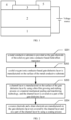
- FIG. 1 schematically shows a structural schematic diagram of a solid oxygen ionic conductor based field-effect transistor according to embodiments of the present disclosure.
- a solid oxygen ionic conductor based field-effect transistor includes: a substrate 1, a gate dielectric layer 2, a channel layer 3, a source electrode 4 and a drain electrode 5.
- the gate dielectric layer 2 is located on the substrate 1, and the gate dielectric layer 2 is a solid-sate oxygen ionic conductor thin film; the channel layer 3 is covered on a part of the gate dielectric layer 2, and the channel layer 3 is an oxide thin film or a thin flake; and the source electrode 4 and the drain electrode 5 are respectively located on the gate dielectric layer 2 not covered by the channel layer 3 and on a part of the channel layer 3.
- the substrate 1 is a metal conductive substrate, including but not limited to one of niobium-doped strontium titanate (Nb doped SrTiO 3 ) or indium tin oxide (ITO) conductive glass.
- the metal conductive substrate may be used as the gate electrode.
- the gate dielectric layer 2 is the solid oxygen ionic conductor thin film, and the material of the solid-state oxygen ionic conductor film is gadolinium-doped ceric oxide (Gd doped CeO 2 ).
- the thickness of the gate dielectric layer 2 is in a range of 400 nm to 1 ⁇ m. On the one hand, the thickness may ensure that the gate dielectric layer is not easily broken down. On the other hand, the thickness may enable growth time of the gate dielectric thin film not to be too long, and may not easily damage the target.
- the gadolinium-doped ceric oxide Compared with other solid-sate oxygen ionic conductors, the gadolinium-doped ceric oxide has a considerable oxygen ion conductivity at room temperature and may regulate the physical properties of oxides at room temperature.
- the channel layer 3 is the oxide thin film or the thin flake, including but not limited to one of copper oxide, strontium cobaltate (SrCoO 2.5 ) and strontium iridium oxide (Sr 2 IrO 4 ), and the thickness of the channel layer 3 is in a range of 5 nm to 30 nm.
- both of the source electrode 4 and the drain electrode 5 are metal elemental films or indium tin oxide conductive films.
- the use of a solid oxygen ion conductor as the gate dielectric layer may solve the problem of electrochemical instability between the gate dielectric and the oxide material, and the physical properties of oxides may be effectively regulated.
- the present disclosure further provides a method of manufacturing a solid oxygen ionic conductor based field-effect transistor.
- FIG. 2 schematically shows a flowchart of a method of manufacturing a solid oxygen ionic conductor based field-effect transistor according to embodiments of the present disclosure. As shown in FIG. 2 , the method includes operations S201 to S204.
- a metal conductive substrate is provided as the gate electrode of the solid oxygen ionic conductor based field-effect transistor.
- the metal conductive substrate may be niobium-doped strontium titanate or indium tin oxide conductive glass.
- the oxygen plasma cleaning is performed on the metal conductive substrate to prepare for the growth of the gate dielectric layer.
- the gate dielectric layer is grown on the metal conductive substrate by using the thin film growth process.
- the thin film growth process includes but is not limited to magnetron sputtering process or pulsed laser deposition process.
- the process of manufacturing the gate dielectric layer by using the magnetron sputtering process is that:
- the process gas is argon, and the reaction gas is oxygen.
- the use of the solid-state oxygen ionic conductor as the gate dielectric layer may solve the problem of electrochemical instability between the gate dielectric layer and the channel layer oxide material.
- the use of the solid-state oxygen ionic conductor may be easily applied to the device, and the back gate configuration of the field-effect transistor may be easily characterized.
- a channel layer is manufactured on the surface of the gate dielectric layer by using a thin film growing and etching process or a material mechanical peeling and transferring technology, and the channel layer is covered on a part of the gate dielectric layer.
- the channel layer is manufactured on the gate dielectric layer, and part of the channel layer is etched by using the thin film growth etching process, including but not limited to argon ion etching process, reactive ion beam etching process or focused ion beam etching process, so as to expose part of the gate dielectric layer for manufacturing the source electrode and the drain electrode.
- the thin film growth etching process including but not limited to argon ion etching process, reactive ion beam etching process or focused ion beam etching process, so as to expose part of the gate dielectric layer for manufacturing the source electrode and the drain electrode.
- oxide materials such as bismuth strontium calcium copper oxide, strontium iridium oxide, and the like that are required to manufacture the channel layer are selected in advance by using the material mechanical peeling and transferring technology, and the oxide materials are transferred to the gate dielectric layer of the solid-state oxygen ionic conductor thin film by the dry transfer or wet transfer technology to form the channel layer.
- the channel layer covers part of the gate dielectric layer, and the gate dielectric layer not covered by the channel layer is used to manufacture the source electrode and drain electrode.
- a source electrode and a drain electrode are manufactured on the gate dielectric layer not covered by the channel layer and on a part of the channel layer by using a coating process.
- the coating process includes electron beam evaporation process or thermal evaporation process.
- the use of the solid-state oxygen ionic conductor as the gate dielectric layer may solve the problem of electrochemical instability between the gate dielectric and the oxide material, making it easy to apply to devices, and able to regulate the physical properties of oxides at room temperature.
- the movement of oxygen ions is a mechanism of vacancies or gaps, both of which are conductive mechanisms of the body, independent of surface adsorption and working environment. Since the oxide thin film is relatively stable under voltage and has a wide electrochemical window, a wide range of carrier concentration regulation may be realized.
- the injected oxygen ions are not impurities and may not destroy the structure of the material, making it a clean regulatory method.
- the material of the channel layer is Bi 2 Sr 2 CaCu 2 O 8+ ⁇ thin layer, and a solid oxygen ionic conductor based field-effect transistor thereof is manufactured according to the following steps S1 to S4.
- niobium-doped strontium titanate (Nb doped SrTiO 3 ) is selected as the substrate with a thickness of 0.5 mm and a size of 5 ⁇ 5 mm 2 , and the oxygen plasma cleaning is performed at a power of 150 W for 10 minutes.
- the gadolinium-doped ceric oxide (Gd doped CeO 2 ) thin film with a thickness of 700 nm is grown as the gate dielectric layer on the niobium-doped strontium titanate substrate by using the magnetron sputtering film growth process.
- process conditions for manufacturing the gate dielectric layer are as follows: the gadolinium-doped ceric oxide is used as the target, the distance between the target and the substrate is 10 cm, the temperature of the substrate is 700 °C, the total pressure of vacuum chamber is 1.2 Pa, the flow ratio of argon to oxygen introduced is 3: 1, the sputtering power is 60 W, and growth time is 12 hours.
- a piece of Bi 2 Sr 2 CaCu 2 O 8+ ⁇ single crystal is selected, stuck on an adhesive tape, and then stuck on a polydimethylsiloxane (PDMS) thin film after repeatedly cleaving with the adhesive tape, a thin-layer sample with a thickness of 9 nm, a length of 30 ⁇ m and a width of 20 ⁇ m is found under an optical microscope after tearing off the adhesive tape. Then, the thin-layer sample is transferred using a transfer table from the polydimethylsiloxane thin film to a surface on which the gadolinium-doped ceric oxide thin film is used as the gate dielectric layer as the channel layer by using a dry transfer method.
- PDMS polydimethylsiloxane
- an Au film is deposited as the source electrode and the drain electrode on the surface on which the gadolinium-doped ceric oxide thin film is used as the gate dielectric layer and which is not covered by the channel layer and on a part of the channel layer by using the thermal evaporation process.
- the Au film has a thickness of 30 nm and an evaporation rate of 0.3 ⁇ /s.
- a field-effect transistor with a back gate structure in which a gadolinium-doped ceric oxide solid-state oxygen ionic conductor film is used as the gate dielectric layer and Bi 2 Sr 2 CaCu 2 O 8+ ⁇ thin layer is used as the channel layer may be acquired through the above-mentioned steps.
- FIG. 3 schematically shows the temperature dependent resistance of the channel material Bi 2 Sr 2 CaCu 2 O 8+ ⁇ thin layer under different gate voltages according to Embodiment 1 of the present disclosure.
- the sample when no bias voltage is applied, the sample is superconducting, and the zero resistance temperature of the sample is 85 K, which is close to the optimal doping.
- a positive bias voltage of 6 V When a positive bias voltage of 6 V is applied, the electric field drives oxygen out of the sample, and the sample is doped with electrons. The room temperature resistance of the sample increases by an order of magnitude, and a cooling shows that the sample becomes an insulator. Then, a negative bias voltage is applied to the sample. Under the applied electric field, oxygen ions in the gadolinium-doped ceric oxide thin film are injected into the sample, the sample is hole-doped, and the sample gradually changes from the insulating state to the superconducting state.
- the bias voltage is -2 V
- the sample realize the optimal superconductivity with a zero resistance temperature of 90 K.
- the bias voltage is -4 V
- the sample is in an over-doped state, and the zero resistance temperature drops to 81 K.
- the material of the channel layer is SrCoO 2.5 thin film, and a solid oxygen ionic conductor based field-effect transistor thereof is manufactured according to the following steps.
- niobium-doped strontium titanate (Nb doped SrTiO 3 ) is selected as the substrate with a thickness of 0.5 mm and a size of 5 ⁇ 5 mm 2 , and the oxygen plasma cleaning is performed at a power of 150 W for 10 minutes.
- the gadolinium-doped ceric oxide (Gd doped CeO 2 ) thin film with a thickness of 1 ⁇ m is grown as the gate dielectric layer on the niobium-doped strontium titanate substrate by using the magnetron sputtering film growth process.
- process conditions for manufacturing the gate dielectric layer are as follows: the gadolinium-doped ceric oxide is used as the target, the distance between the target and the substrate is 10 cm, the temperature of the substrate is 700 °C, the total pressure of a vacuum chamber is 1.2 Pa, the flow ratio of argon to oxygen introduced is 3: 1, the sputtering power is 60 W, and growth time is 18 hours.
- SrCoO 2.5 thin film with thickness of 30 nm is grown on the gadolinium-doped ceric oxide thin film by using the magnetron sputtering thin film growth process.
- process conditions for manufacturing the channel layer are as follows: strontium cobaltate is used as the target, the distance between the target and the substrate is 5 cm, the temperature of the substrate is 750 °C, the total pressure of the vacuum chamber is 12 Pa, the flow ratio of argon to oxygen introduced is 9: 1, the sputtering power is 50W, and the growth time is 20 minutes.
- the SrCoO 2.5 thin film is etched into a size of 100 ⁇ m in length and 50 ⁇ m in width by the argon ion etching process as the channel layer.
- the chromium/gold (Cr/Au) composite film is deposited as the source electrode and the drain electrode on the surface on which the gadolinium-doped ceric oxide thin film is used as the gate dielectric layer and which is not covered by the channel layer and on a part of the channel layer by using the electron beam evaporation process.
- the chromium (Cr) film has a thickness of 5 nm and an evaporation rate of 0.1 angstrom per second (A/s); the gold (Cr/Au) film has a thickness of 50 nm and an evaporation rate of 0.3 ⁇ /s.
- a field-effect transistor with a back gate structure in which a gadolinium-doped ceric oxide solid-state oxygen ionic conductor film is used as the gate dielectric layer and SrCoO 2.5 thin film is used as the channel layer may be acquired through the above-mentioned steps.
- FIG. 4 schematically shows the temperature dependent resistance of the channel material SrCoO 2.5 thin film under different gate voltages according to Embodiment 2 of the present disclosure.
- the sample when no bias voltage is applied, the sample is a strong insulator.
- a negative bias voltage is applied to the sample, under the applied electric field, oxygen ions in the gadolinium-doped ceric oxide thin film are injected into the sample, the sample is hole-doped.
- the oxygen content of the sample is changed, and the sample gradually changes from an insulating state to a metallic state.
- a further measurement shows that the sample changes from an antiferromagnetic insulator to a ferromagnetic metal, and the room temperature resistance of the sample decreases by four orders of magnitude.
- the material of the channel layer is Sr 2 IrO 4 thin film, and a solid oxygen ionic conductor based field-effect transistor thereof is manufactured according to the following steps S 1 to S4.
- niobium-doped strontium titanate (Nb doped SrTiO 3 ) is selected as the substrate with a thickness of 0.5 mm and a size of 5 ⁇ 5 mm 2 , and the oxygen plasma cleaning is performed at a power of 150 W for 10 minutes.
- the gadolinium-doped ceric oxide (Gd doped CeO 2 ) thin film with a thickness of 400 nm is grown as the gate dielectric layer on the niobium-doped strontium titanate substrate by using the magnetron sputtering film growth process.
- process conditions for manufacturing the gate dielectric layer are as follows: the gadolinium-doped ceric oxide is used as the target, the distance between the target and the substrate is 10 cm, the temperature of the substrate is 600 °C, the total pressure of a vacuum chamber is 1.2 Pa, the flow ratio of argon to oxygen introduced is 2:1, the sputtering power is 50 W, and growth time is 8 hours.
- the Sr 2 IrO 4 thin film grown on a water-soluble substrate is transferred to the polydimethylsiloxane (PDMS) thin film by using a wet transfer method, a thin film sample with a thickness of 8 unit cells, a length of 20 ⁇ m and a width of 15 ⁇ m is selected under an optical microscope, and then the sample is transferred using a transfer table from the polydimethylsiloxane thin film to the surface on which the gadolinium-doped ceric oxide thin film is used as the gate dielectric layer as the channel layer by using a dry transfer method.
- PDMS polydimethylsiloxane
- an indium tin oxide/gold (ITO/Au) composite film is deposited as the source electrode and the drain electrode on the surface on which the gadolinium-doped ceric oxide thin film is used as the gate dielectric layer and which is not covered by the channel layer and on a part of the channel layer by using the electron beam evaporation process.
- the indium tin oxide (ITO) film has a thickness of 10 nm and an evaporation rate of 0.2 angstrom per second (A/s).
- the gold (Au) film has a thickness of 50 nm and an evaporation rate of 0.3 ⁇ /s, and the temperature of a plating plate is 60 °C.
- a field-effect transistor with a back gate structure in which a gadolinium-doped ceric oxide solid-state oxygen ionic conductor film is used as the gate dielectric layer and the Sr 2 IrO 4 thin film is used as the channel layer may be acquired through the above-mentioned steps.
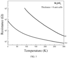
- FIG. 5 schematically shows the temperature dependent resistance of the channel material Sr 2 IrO 4 thin film under different gate voltages according to Embodiment 3 of the present disclosure.
- the sample when no bias voltage is applied, the sample is a strong insulator.
- oxygen ions in the gadolinium-doped ceric oxide thin film may be far away from the sample, leaving a positive charge background near the sample, and will electrostatically regulate electrons to gather on the surface of the sample near the dielectric layer, so as to conduct electron doping on the sample.
- the electric field increases to a certain level, oxygen in the sample may be removed, and at the same time, the oxygen content of the sample may also be changed, gradually weakening the insulation of the sample.
Landscapes
- Engineering & Computer Science (AREA)
- Manufacturing & Machinery (AREA)
- Chemical & Material Sciences (AREA)
- Materials Engineering (AREA)
- Physics & Mathematics (AREA)
- Formation Of Insulating Films (AREA)
- Inorganic Compounds Of Heavy Metals (AREA)
- Optics & Photonics (AREA)
- Plasma & Fusion (AREA)
- Thin Film Transistor (AREA)
- Physical Vapour Deposition (AREA)
Abstract
Description
- The present disclosure relates to fields of physics, material science and semiconductor technology, and in particular, to a new solid oxygen ionic conductor-based field effect transistor and its manufacturing method.
- Regulating physical properties of oxides is a hot topic in the study of the condensed matter physics, and how to realize effective regulation of physical properties has always been a research focus of scientists. Electrostatic regulation of carrier concentration in oxide materials is an effective method to control the physical property of oxides. By simply changing the DC bias voltage, it is easy to control carrier concentration without introducing structural disorder like chemical doping. Unfortunately, due to a low dielectric constant and a breakdown voltage, the maximum carrier concentration introduced by a traditional all-solid-state field-effect transistor that uses solid-state oxides such as silicon dioxide, strontium titanate and the like as gate dielectrics is less than 1013 cm-2. In order to overcome these limitations, non-solid-state electrolytes, including the ionic liquid and the ionic gel, have been used in the electric-double-layer field-effect transistor, and the adjustable carrier concentration has reached 1014 cm-2. However, due to the liquid nature of the electrolyte, there are great limitations on the stability, characterization and device application of the material.
- The solid-state proton conductor based field-effect transistor developed by using porous solid-state oxide proton conductor films such as silicon dioxide, alumina and the like as solid-state electrolytes avoids use of liquids, but still has problems. Because the proton conductivity of the porous solid-state oxide proton conductor films is easily lost, the proton conductivity only exists when water molecules are adsorbed on the surface of the thin film, thus extremely depending on the surrounding gas atmosphere. In addition, because of the water decomposition, compared with other electrolytes, the electrochemical window of porous solid-state oxide proton conductor film is very small, only 1.23 V, which may limit its regulation ability.
- Patent "Method for Regulating Carrier Concentration of Material, Field Effect Transistor and Manufacturing Method" (Patent No.
201610585699.1 - In recent years, ionic liquids have another application. With the ionic liquid as the gate dielectric, the oxide has been tuned by electric field under an applied bias voltage at room temperature. Residual water in the ionic liquid may be electrolyzed into protons and oxygen ions, and the oxygen ions may diffuse into the oxide, and thus effectively regulate the physical properties of the oxide. However, the electrolyte used in this method is still liquid, which may greatly limit the stability of the sample, the characterization and the application of the device. In addition, the regulation of the physical property by electrolyzing the residual water in the ionic liquid into protons and oxygen ions may be caused by the uneven diffusion of its concentration, and the regulation is uncontrollable and irreversible, In addition, the oxygen ion has a large ionic radius and a long diffusion time, so it usually takes several days to realize a considerable regulatory effect, which may limit their application in devices.
- In summary, the existing electric field control technology of field-effect transistor has some defects and limitations to some extent for the oxide.
- In view of this, in order to effectively regulate the physical properties of oxides, the present disclosure provides a new solid oxygen ionic conductor based field-effect transistor and its manufacturing method.
- In order to realize the above-mentioned objects, on one hand, the present disclosure provides a solid oxygen ionic conductor based field-effect transistor, including:
a substrate; a gate dielectric layer located on the substrate, where the gate dielectric layer is a solid oxygen ionic conductor thin film; a channel layer covered on a part of the gate dielectric layer; and a source electrode and a drain electrode respectively located on the gate dielectric layer not covered by the channel layer and on a part of the channel layer. - According to embodiments of the present disclosure, the substrate is a metal conductive substrate, including one of niobium-doped strontium titanate or indium tin oxide conductive glass.
- According to embodiments of the present disclosure, the material of the solid oxygen ionic conductor thin film is gadolinium-doped ceric oxide; and the thickness of the gate dielectric layer is in a range of 400 nm to 1 µm.
- According to embodiments of the present disclosure, the material of the channel layer is an oxide thin film or thin flake, including one of: copper oxide, strontium cobaltate, or strontium iridium oxide; and the thickness of the channel layer is in a range of 5 nm to 30 nm.
- According to embodiments of the present disclosure, both of the source and drain electrodes are one of the metal elemental films or indium tin oxide conductive films.
- On the other hand, the present disclosure further provides a method of manufacturing a field-effect transistor, including: providing a metal conductive substrate as the gate electrode of the field-effect transistor; manufacturing a solid oxygen ionic conductor based gate dielectric layer on the surface of the metal conductive substrate; manufacturing a channel layer on the surface of the gate dielectric layer by using thin film growing and etching process or material mechanical peeling and transferring technology, which covers a partion of the gate dielectric layer; and manufacturing a source electrode and a drain electrode on the gate dielectric layer not covered by the channel layer and on a part of the channel layer by using a coating process.
- According to embodiments of the present disclosure, the preparation process of manufacturing the solid oxygen ionic conductor based gate dielectric layer on the surface of the metal conductive substrate includes one of magnetron sputtering or pulsed laser deposition.
- According to embodiments of the present disclosure, the preparation process of manufacturing the gate dielectric layer includes that: the temperature at which the metal conductive substrate is heated is in a range of 600 °C to 750 °C; the power density is in a range of 1.5 W/cm2 to 3.5 W/cm2; the distance between the target and the metal conductive substrate is in a range of 5 cm to 12 cm; and the gas flow ratio of process gas to reaction gas is in a range of 2:1 to 3:1.
- According to embodiments of the present disclosure, the process gas is argon and the reaction gas is oxygen.
- According to embodiments of the present disclosure, the thin film growing and etching process includes one of the argon ion etching process, reactive ion beam etching process or focused ion beam etching process; the material mechanical peeling and transferring technology includes one of dry transfer or wet transfer; and the coating process includes one of electron beam evaporation process or thermal evaporation process.
- According to embodiments of the present disclosure, the use of solid-state oxygen ionic conductor as the gate dielectric layer may solve the problem of electrochemical instability between the gate dielectric and the oxide material, making it easy to apply to devices, and able to regulate the physical properties of oxides at room temperature. The movement of oxygen ions is a mechanism of vacancies or gaps, both of which are conductive mechanisms of the body, independent of surface adsorption and working environment. Since the oxide thin film is relatively stable under voltage and has a wide electrochemical window, a wide range of carrier concentration regulation may be realized. For oxides, the injected oxygen ions are not impurities and may not destroy the structure of the material, making it a clean regulatory method.
-
-
FIG. 1 schematically shows the structural schematic diagram of a solid oxygen ionic conductor based field-effect transistor according to embodiments of the present disclosure; -
FIG. 2 schematically shows a flowchart of a method of manufacturing a solid oxygen ionic conductor based field-effect transistor according to embodiments of the present disclosure; -
FIG. 3 schematically shows the temperature dependent resistance of the channel material Bi2Sr2CaCu2O8+δ thin layer under different gate voltages according toEmbodiment 1 of the present disclosure; -
FIG. 4 schematically shows the temperature dependent resistance of the channel material SrCoO2.5 thin film under different gate voltages according toEmbodiment 2 of the present disclosure; -
FIG. 5 schematically shows the temperature dependent resistance of the channel material Sr2IrO4 thin film under different gate voltages according toEmbodiment 3 of the present disclosure. - In order to make objectives, technical solutions and advantages of the present disclosure clearer, the present disclosure will be further described in detail below with reference to the specific embodiments and accompanying drawings.
- It should be noted that the accompanying drawings of the specification, which constitute a part of the present disclosure, are used to provide a further understanding of the present disclosure, and illustrative embodiments of the present disclosure and descriptions thereof are intended to explain the present disclosure and do not constitute an improper limitation on the present disclosure.
FIG. 1 schematically shows a structural schematic diagram of a solid oxygen ionic conductor based field-effect transistor according to embodiments of the present disclosure. - As shown in
FIG. 1 , a solid oxygen ionic conductor based field-effect transistor provided by the present disclosure includes: asubstrate 1, a gatedielectric layer 2, achannel layer 3, asource electrode 4 and adrain electrode 5. The gatedielectric layer 2 is located on thesubstrate 1, and the gatedielectric layer 2 is a solid-sate oxygen ionic conductor thin film; thechannel layer 3 is covered on a part of the gatedielectric layer 2, and thechannel layer 3 is an oxide thin film or a thin flake; and thesource electrode 4 and thedrain electrode 5 are respectively located on the gatedielectric layer 2 not covered by thechannel layer 3 and on a part of thechannel layer 3. - According to embodiments of the present disclosure, the
substrate 1 is a metal conductive substrate, including but not limited to one of niobium-doped strontium titanate (Nb doped SrTiO3) or indium tin oxide (ITO) conductive glass. The metal conductive substrate may be used as the gate electrode. - According to embodiments of the present disclosure, the gate
dielectric layer 2 is the solid oxygen ionic conductor thin film, and the material of the solid-state oxygen ionic conductor film is gadolinium-doped ceric oxide (Gd doped CeO2). - According to embodiments of the present disclosure, the thickness of the gate
dielectric layer 2 is in a range of 400 nm to 1 µm. On the one hand, the thickness may ensure that the gate dielectric layer is not easily broken down. On the other hand, the thickness may enable growth time of the gate dielectric thin film not to be too long, and may not easily damage the target. - Compared with other solid-sate oxygen ionic conductors, the gadolinium-doped ceric oxide has a considerable oxygen ion conductivity at room temperature and may regulate the physical properties of oxides at room temperature.
- According to embodiments of the present disclosure, the
channel layer 3 is the oxide thin film or the thin flake, including but not limited to one of copper oxide, strontium cobaltate (SrCoO2.5) and strontium iridium oxide (Sr2IrO4), and the thickness of thechannel layer 3 is in a range of 5 nm to 30 nm. - According to embodiments of the present disclosure, both of the
source electrode 4 and thedrain electrode 5 are metal elemental films or indium tin oxide conductive films. - According to embodiments of the present disclosure, by providing a new solid-state oxygen ionic conductor based field-effect transistor, the use of a solid oxygen ion conductor as the gate dielectric layer may solve the problem of electrochemical instability between the gate dielectric and the oxide material, and the physical properties of oxides may be effectively regulated.
- Based on the above-mentioned solid oxygen ionic conductor based field-effect transistor, the present disclosure further provides a method of manufacturing a solid oxygen ionic conductor based field-effect transistor.
-
FIG. 2 schematically shows a flowchart of a method of manufacturing a solid oxygen ionic conductor based field-effect transistor according to embodiments of the present disclosure. As shown inFIG. 2 , the method includes operations S201 to S204. - In operation S201, a metal conductive substrate is provided as the gate electrode of the solid oxygen ionic conductor based field-effect transistor.
- According to embodiments of the present disclosure, the metal conductive substrate may be niobium-doped strontium titanate or indium tin oxide conductive glass. The oxygen plasma cleaning is performed on the metal conductive substrate to prepare for the growth of the gate dielectric layer.
- In operation S202, a solid oxygen ionic conductor based gate dielectric layer is manufactured on the surface of the metal conductive substrate.
- According to embodiments of the present disclosure, the gate dielectric layer is grown on the metal conductive substrate by using the thin film growth process. The thin film growth process includes but is not limited to magnetron sputtering process or pulsed laser deposition process.
- According to embodiments of the present disclosure, the process of manufacturing the gate dielectric layer by using the magnetron sputtering process is that:
- a temperature at which the metal conductive substrate is heated is in a range of 600 °C to 750 °C;
- a power density is in a range of 1.5 W/cm2 to 3.5 W/cm2;
- a distance between a target and the metal conductive substrate is in a range of 5 cm to 12 cm; and
- a gas flow ratio of process gas to reaction gas is in a range of 2:1 to 3:1.
- According to embodiments of the present disclosure, the process gas is argon, and the reaction gas is oxygen.
- According to embodiments of the present disclosure, the use of the solid-state oxygen ionic conductor as the gate dielectric layer may solve the problem of electrochemical instability between the gate dielectric layer and the channel layer oxide material. At the same time, the use of the solid-state oxygen ionic conductor may be easily applied to the device, and the back gate configuration of the field-effect transistor may be easily characterized.
- In operation S203, a channel layer is manufactured on the surface of the gate dielectric layer by using a thin film growing and etching process or a material mechanical peeling and transferring technology, and the channel layer is covered on a part of the gate dielectric layer.
- According to embodiments of the present disclosure, the channel layer is manufactured on the gate dielectric layer, and part of the channel layer is etched by using the thin film growth etching process, including but not limited to argon ion etching process, reactive ion beam etching process or focused ion beam etching process, so as to expose part of the gate dielectric layer for manufacturing the source electrode and the drain electrode.
- Alternatively, a certain size of oxide materials, such as bismuth strontium calcium copper oxide, strontium iridium oxide, and the like that are required to manufacture the channel layer are selected in advance by using the material mechanical peeling and transferring technology, and the oxide materials are transferred to the gate dielectric layer of the solid-state oxygen ionic conductor thin film by the dry transfer or wet transfer technology to form the channel layer. The channel layer covers part of the gate dielectric layer, and the gate dielectric layer not covered by the channel layer is used to manufacture the source electrode and drain electrode.
- In operation S204, a source electrode and a drain electrode are manufactured on the gate dielectric layer not covered by the channel layer and on a part of the channel layer by using a coating process.
- According to embodiments of the present disclosure, the coating process includes electron beam evaporation process or thermal evaporation process.
- According to embodiments of the present disclosure, the use of the solid-state oxygen ionic conductor as the gate dielectric layer may solve the problem of electrochemical instability between the gate dielectric and the oxide material, making it easy to apply to devices, and able to regulate the physical properties of oxides at room temperature. The movement of oxygen ions is a mechanism of vacancies or gaps, both of which are conductive mechanisms of the body, independent of surface adsorption and working environment. Since the oxide thin film is relatively stable under voltage and has a wide electrochemical window, a wide range of carrier concentration regulation may be realized. For oxides, the injected oxygen ions are not impurities and may not destroy the structure of the material, making it a clean regulatory method.
- In order to more clearly describe the method of manufacturing the solid-state oxygen ionic conductor based field-effect transistor of the present disclosure, the present disclosure provides specific embodiments for further specific explanation. It should be noted that the descriptions of these specific embodiments are only exemplary, and are not intended to limit the scope of protection of the present disclosure.
- In the embodiment, the material of the channel layer is Bi2Sr2CaCu2O8+δ thin layer, and a solid oxygen ionic conductor based field-effect transistor thereof is manufactured according to the following steps S1 to S4.
- In S1, niobium-doped strontium titanate (Nb doped SrTiO3) is selected as the substrate with a thickness of 0.5 mm and a size of 5×5 mm2, and the oxygen plasma cleaning is performed at a power of 150 W for 10 minutes.
- In S2, the gadolinium-doped ceric oxide (Gd doped CeO2) thin film with a thickness of 700 nm is grown as the gate dielectric layer on the niobium-doped strontium titanate substrate by using the magnetron sputtering film growth process.
- According to embodiments of the present disclosure, process conditions for manufacturing the gate dielectric layer are as follows: the gadolinium-doped ceric oxide is used as the target, the distance between the target and the substrate is 10 cm, the temperature of the substrate is 700 °C, the total pressure of vacuum chamber is 1.2 Pa, the flow ratio of argon to oxygen introduced is 3: 1, the sputtering power is 60 W, and growth time is 12 hours.
- In S3, a piece of Bi2Sr2CaCu2O8+δsingle crystal is selected, stuck on an adhesive tape, and then stuck on a polydimethylsiloxane (PDMS) thin film after repeatedly cleaving with the adhesive tape, a thin-layer sample with a thickness of 9 nm, a length of 30 µm and a width of 20 µm is found under an optical microscope after tearing off the adhesive tape. Then, the thin-layer sample is transferred using a transfer table from the polydimethylsiloxane thin film to a surface on which the gadolinium-doped ceric oxide thin film is used as the gate dielectric layer as the channel layer by using a dry transfer method.
- In S4, an Au film is deposited as the source electrode and the drain electrode on the surface on which the gadolinium-doped ceric oxide thin film is used as the gate dielectric layer and which is not covered by the channel layer and on a part of the channel layer by using the thermal evaporation process. The Au film has a thickness of 30 nm and an evaporation rate of 0.3 Å/s.
- According to embodiments of the present disclosure, a field-effect transistor with a back gate structure in which a gadolinium-doped ceric oxide solid-state oxygen ionic conductor film is used as the gate dielectric layer and Bi2Sr2CaCu2O8+δ thin layer is used as the channel layer may be acquired through the above-mentioned steps.
- In order to verify the regulation performance of the field-effect transistor on the channel material, the device is placed in a comprehensive physical property measurement system (PPMS), vacuum is pumped to less than 1 millibar, temperature is stabilized at 300 K, the bias voltage is applied between the gate electrode and the source electrode by using a digital source meter, and the resistance of the channel material is measured by using a lock-in amplifier. For example,
FIG. 3 schematically shows the temperature dependent resistance of the channel material Bi2Sr2CaCu2O8+δ thin layer under different gate voltages according toEmbodiment 1 of the present disclosure. - As shown in
FIG. 3 , when no bias voltage is applied, the sample is superconducting, and the zero resistance temperature of the sample is 85 K, which is close to the optimal doping. When a positive bias voltage of 6 V is applied, the electric field drives oxygen out of the sample, and the sample is doped with electrons. The room temperature resistance of the sample increases by an order of magnitude, and a cooling shows that the sample becomes an insulator. Then, a negative bias voltage is applied to the sample. Under the applied electric field, oxygen ions in the gadolinium-doped ceric oxide thin film are injected into the sample, the sample is hole-doped, and the sample gradually changes from the insulating state to the superconducting state. When the bias voltage is -2 V, the sample realize the optimal superconductivity with a zero resistance temperature of 90 K. When the bias voltage is -4 V, the sample is in an over-doped state, and the zero resistance temperature drops to 81 K. - From an experimental result, it can be seen that the physical properties of the channel material has been well regulated by the electric field, which shows the excellent performance of the solid oxygen ionic conductor based field-effect transistor.
- In the embodiment, the material of the channel layer is SrCoO2.5 thin film, and a solid oxygen ionic conductor based field-effect transistor thereof is manufactured according to the following steps.
- In S1, niobium-doped strontium titanate (Nb doped SrTiO3) is selected as the substrate with a thickness of 0.5 mm and a size of 5×5 mm2, and the oxygen plasma cleaning is performed at a power of 150 W for 10 minutes.
- In S2, the gadolinium-doped ceric oxide (Gd doped CeO2) thin film with a thickness of 1 µm is grown as the gate dielectric layer on the niobium-doped strontium titanate substrate by using the magnetron sputtering film growth process.
- According to embodiments of the present disclosure, process conditions for manufacturing the gate dielectric layer are as follows: the gadolinium-doped ceric oxide is used as the target, the distance between the target and the substrate is 10 cm, the temperature of the substrate is 700 °C, the total pressure of a vacuum chamber is 1.2 Pa, the flow ratio of argon to oxygen introduced is 3: 1, the sputtering power is 60 W, and growth time is 18 hours.
- In S3, SrCoO2.5 thin film with thickness of 30 nm is grown on the gadolinium-doped ceric oxide thin film by using the magnetron sputtering thin film growth process.
- According to embodiments of the present disclosure, process conditions for manufacturing the channel layer are as follows: strontium cobaltate is used as the target, the distance between the target and the substrate is 5 cm, the temperature of the substrate is 750 °C, the total pressure of the vacuum chamber is 12 Pa, the flow ratio of argon to oxygen introduced is 9: 1, the sputtering power is 50W, and the growth time is 20 minutes.
- In S4, the SrCoO2.5 thin film is etched into a size of 100 µm in length and 50 µm in width by the argon ion etching process as the channel layer.
- In S5, the chromium/gold (Cr/Au) composite film is deposited as the source electrode and the drain electrode on the surface on which the gadolinium-doped ceric oxide thin film is used as the gate dielectric layer and which is not covered by the channel layer and on a part of the channel layer by using the electron beam evaporation process. The chromium (Cr) film has a thickness of 5 nm and an evaporation rate of 0.1 angstrom per second (A/s); the gold (Cr/Au) film has a thickness of 50 nm and an evaporation rate of 0.3 Å/s.
- According to embodiments of the present disclosure, a field-effect transistor with a back gate structure in which a gadolinium-doped ceric oxide solid-state oxygen ionic conductor film is used as the gate dielectric layer and SrCoO2.5 thin film is used as the channel layer may be acquired through the above-mentioned steps.
- In order to verify the regulation performance of the field-effect transistor on the channel material, the device is placed in a comprehensive physical property measurement system (PPMS), vacuum is pumped to less than 1 millibar, temperature is stabilized at 300 K, the bias voltage is applied between the gate electrode and the source electrode by using a digital source meter, and the resistance of the channel material is measured by using a lock-in amplifier. For example,
FIG. 4 schematically shows the temperature dependent resistance of the channel material SrCoO2.5 thin film under different gate voltages according toEmbodiment 2 of the present disclosure. - As shown in
FIG. 4 , when no bias voltage is applied, the sample is a strong insulator. When a negative bias voltage is applied to the sample, under the applied electric field, oxygen ions in the gadolinium-doped ceric oxide thin film are injected into the sample, the sample is hole-doped. At the same time, the oxygen content of the sample is changed, and the sample gradually changes from an insulating state to a metallic state. A further measurement shows that the sample changes from an antiferromagnetic insulator to a ferromagnetic metal, and the room temperature resistance of the sample decreases by four orders of magnitude. - From an experimental result, it can be seen that the physical properties of the channel material has been well regulated by the electric field, which shows the excellent performance of the solid oxygen ionic conductor based field-effect transistor.
- In the embodiment, the material of the channel layer is Sr2IrO4 thin film, and a solid oxygen ionic conductor based field-effect transistor thereof is manufactured according to the following steps S 1 to S4.
- In
S 1, niobium-doped strontium titanate (Nb doped SrTiO3) is selected as the substrate with a thickness of 0.5 mm and a size of 5×5 mm2, and the oxygen plasma cleaning is performed at a power of 150 W for 10 minutes. - In S2, the gadolinium-doped ceric oxide (Gd doped CeO2) thin film with a thickness of 400 nm is grown as the gate dielectric layer on the niobium-doped strontium titanate substrate by using the magnetron sputtering film growth process.
- According to embodiments of the present disclosure, process conditions for manufacturing the gate dielectric layer are as follows: the gadolinium-doped ceric oxide is used as the target, the distance between the target and the substrate is 10 cm, the temperature of the substrate is 600 °C, the total pressure of a vacuum chamber is 1.2 Pa, the flow ratio of argon to oxygen introduced is 2:1, the sputtering power is 50 W, and growth time is 8 hours.
- In S3, the Sr2IrO4 thin film grown on a water-soluble substrate is transferred to the polydimethylsiloxane (PDMS) thin film by using a wet transfer method, a thin film sample with a thickness of 8 unit cells, a length of 20 µm and a width of 15 µm is selected under an optical microscope, and then the sample is transferred using a transfer table from the polydimethylsiloxane thin film to the surface on which the gadolinium-doped ceric oxide thin film is used as the gate dielectric layer as the channel layer by using a dry transfer method.
- In S4, an indium tin oxide/gold (ITO/Au) composite film is deposited as the source electrode and the drain electrode on the surface on which the gadolinium-doped ceric oxide thin film is used as the gate dielectric layer and which is not covered by the channel layer and on a part of the channel layer by using the electron beam evaporation process. The indium tin oxide (ITO) film has a thickness of 10 nm and an evaporation rate of 0.2 angstrom per second (A/s). The gold (Au) film has a thickness of 50 nm and an evaporation rate of 0.3 Å/s, and the temperature of a plating plate is 60 °C.
- According to embodiments of the present disclosure, a field-effect transistor with a back gate structure in which a gadolinium-doped ceric oxide solid-state oxygen ionic conductor film is used as the gate dielectric layer and the Sr2IrO4 thin film is used as the channel layer may be acquired through the above-mentioned steps.
- In order to verify the regulation performance of the field-effect transistor on the channel material, the device is placed in a comprehensive physical property measurement system (PPMS), vacuum is pumped to less than 1 millibar, temperature is stabilized at 300 K, the bias voltage is applied between the gate electrode and the source electrode by using a digital source meter, and the resistance of the channel material is measured by using a lock-in amplifier. For example,
FIG. 5 schematically shows the temperature dependent resistance of the channel material Sr2IrO4 thin film under different gate voltages according toEmbodiment 3 of the present disclosure. - As shown in
FIG. 5 , when no bias voltage is applied, the sample is a strong insulator. When a positive bias is applied to the sample, under the applied electric field, oxygen ions in the gadolinium-doped ceric oxide thin film may be far away from the sample, leaving a positive charge background near the sample, and will electrostatically regulate electrons to gather on the surface of the sample near the dielectric layer, so as to conduct electron doping on the sample. When the electric field increases to a certain level, oxygen in the sample may be removed, and at the same time, the oxygen content of the sample may also be changed, gradually weakening the insulation of the sample. - From an experimental result, it can be seen that although the electric field regulation may not change the sample from an insulating state to a metallic state, the room temperature resistance of the sample has decreased by nearly an order of magnitude, and the low temperature resistance has decreased by several orders of magnitude. This shows that the electric field well regulates the physical properties of the channel material, and shows the excellent performance of the solid oxygen ionic conductor based field-effect transistor.
- The above-mentioned specific embodiments further describe the objectives, technical solutions and beneficial effects of the present disclosure in detail. It should be understood that the above are only specific embodiments of the present disclosure and are not intended to limit the present disclosure. Any modifications, equivalent replacements, improvements, etc. made within the spirit and principles of the present disclosure shall be included in the scope of protection of the present disclosure.
Claims (10)
- A solid oxygen ionic conductor based field-effect transistor, comprising:a substrate;a gate dielectric layer located on the substrate, wherein the gate dielectric layer is a solid oxygen ionic conductor thin film;a channel layer covered on a part of the gate dielectric layer; anda source electrode and a drain electrode respectively located on the gate dielectric layer not covered by the channel layer and on a part of the channel layer.
- The solid oxygen ionic conductor based field-effect transistor according to claim 1, wherein the substrate is a metal conductive substrate, comprising one of niobium-doped strontium titanate or indium tin oxide conductive glass.
- The solid oxygen ionic conductor based field-effect transistor according to claim 1, wherein the material of the solid oxygen ion conductor thin film is gadolinium-doped ceric oxide; and the thickness of the gate dielectric layer is in a range of 400 nm to 1 µm.
- The solid oxygen ionic conductor based field-effect transistor according to claim 1, wherein the material of the channel layer is an oxide thin film or thin flake, comprising one of: copper oxide, strontium cobaltate, or strontium iridium oxide; and the thickness of the channel layer is in a range of 5 nm to 30 nm.
- The solid oxygen ionic conductor based field-effect transistor according to claim 1, wherein both of the source and the drain electrodes are one of the metal elemental films or indium tin oxide conductive films.
- A method of manufacturing a solid oxygen ionic conductor based field-effect transistor according to any one of claims 1 to 5, comprising:providing a metal conductive substrate as a gate electrode of the solid oxygen ionic conductor based field-effect transistor;manufacturing a solid oxygen ionic conductor based gate dielectric layer on the surface of the metal conductive substrate;manufacturing a channel layer on the surface of the gate dielectric layer by using thin film growing and etching process or material mechanical peeling and transferring technology, wherein the channel layer is covered on a part of the gate dielectric layer; andmanufacturing a source electrode and a drain electrode on the gate dielectric layer not covered by the channel layer and on a part of the channel layer by using a coating process.
- The method according to claim 6, wherein the process of manufacturing the solid oxygen ionic conductor based gate dielectric layer on the surface of the metal conductive substrate comprises one of magnetron sputtering or pulsed laser deposition.
- The method according to claim 7, wherein the process of manufacturing the gate dielectric layer comprises:a temperature at which the metal conductive substrate is heated is in a range of 600 °C to 750 °C;a power density is in a range of 1.5 W/cm2 to 3.5 W/cm2;a distance between a target and the metal conductive substrate is in a range of 5 cm to 12 cm; anda gas flow ratio of process gas to reaction gas is in a range of 2:1 to 3:1.
- The method according to claim 8, wherein the process gas is argon and the reaction gas is oxygen.
- The method according to claim 6, wherein the thin film growing and etching process comprises one of the argon ion etching process, reactive ion beam etching process or focused ion beam etching process; the material mechanical peeling and transferring technology comprises one of dry transfer or wet transfer; and the coating process comprises one of electron beam evaporation process or thermal evaporation process.
Applications Claiming Priority (1)
| Application Number | Priority Date | Filing Date | Title |
|---|---|---|---|
| PCT/CN2021/071650 WO2022151122A1 (en) | 2021-01-14 | 2021-01-14 | Solid oxygen ion conductor based field effect transistor and manufacturing method therefor |
Publications (3)
| Publication Number | Publication Date |
|---|---|
| EP4280292A1 true EP4280292A1 (en) | 2023-11-22 |
| EP4280292A4 EP4280292A4 (en) | 2024-10-16 |
| EP4280292B1 EP4280292B1 (en) | 2026-04-29 |
Family
ID=82447724
Family Applications (1)
| Application Number | Title | Priority Date | Filing Date |
|---|---|---|---|
| EP21918333.2A Active EP4280292B1 (en) | 2021-01-14 | 2021-01-14 | Solid oxygen ion conductor based field effect transistor and manufacturing method therefor |
Country Status (3)
| Country | Link |
|---|---|
| US (1) | US20240088240A1 (en) |
| EP (1) | EP4280292B1 (en) |
| WO (1) | WO2022151122A1 (en) |
Family Cites Families (6)
| Publication number | Priority date | Publication date | Assignee | Title |
|---|---|---|---|---|
| KR100576703B1 (en) * | 2003-10-23 | 2006-05-03 | 한국전자통신연구원 | Metal-insulator phase transition high speed switching device and method of manufacturing the same |
| KR100695150B1 (en) * | 2005-05-12 | 2007-03-14 | 삼성전자주식회사 | Transistor using metal-insulator conversion material and manufacturing method thereof |
| JP6191986B2 (en) * | 2013-06-27 | 2017-09-06 | 国立研究開発法人物質・材料研究機構 | Variable electric conduction element using all-solid electric double layer and electronic device using the same |
| CN105633280A (en) * | 2016-02-03 | 2016-06-01 | 中国科学院宁波材料技术与工程研究所 | Mott transistor and fabrication method thereof |
| JP6817600B2 (en) * | 2016-04-28 | 2021-01-20 | パナソニックIpマネジメント株式会社 | 3-terminal element and its manufacturing method |
| CN106024901B (en) * | 2016-07-22 | 2019-07-02 | 中国科学技术大学先进技术研究院 | Method for regulating material carrier concentration, field effect transistor and manufacturing method |
-
2021
- 2021-01-14 WO PCT/CN2021/071650 patent/WO2022151122A1/en not_active Ceased
- 2021-01-14 US US18/271,919 patent/US20240088240A1/en active Pending
- 2021-01-14 EP EP21918333.2A patent/EP4280292B1/en active Active
Also Published As
| Publication number | Publication date |
|---|---|
| US20240088240A1 (en) | 2024-03-14 |
| EP4280292B1 (en) | 2026-04-29 |
| WO2022151122A1 (en) | 2022-07-21 |
| EP4280292A4 (en) | 2024-10-16 |
Similar Documents
| Publication | Publication Date | Title |
|---|---|---|
| CN106024901A (en) | Method for regulating and controlling material carrier concentration, field effect transistor and manufacturing method | |
| CN101548388A (en) | Method for manufacturing thin film transistor which uses an oxide semiconductor | |
| US20160248006A1 (en) | Dopant-driven phase transitions in correlated metal oxides | |
| Hu et al. | Preparation and dielectric properties of dense and amorphous alumina film by sol–gel technology | |
| Atak et al. | Effects of anodic layer thickness on overall performance of all-solid-state electrochromic device | |
| Kondaiah et al. | Substrate temperature influenced ZrO2 films for MOS devices | |
| Wang et al. | Influence of LiPON thickness on the electro-optical performance of inorganic all-solid-state electrochromic devices | |
| EP4280292B1 (en) | Solid oxygen ion conductor based field effect transistor and manufacturing method therefor | |
| van de Krol et al. | Structure and properties of anatase TiO 2 thin films made by reactive electron beam evaporation | |
| CN114765223A (en) | Solid oxygen ion conductor-based field effect transistor and preparation method thereof | |
| Lei et al. | Manipulating high-temperature superconductivity by oxygen doping in Bi2Sr2CaCu2O8+ δ thin flakes | |
| Isidorsson et al. | Ion transport in porous Sn oxide films: Cyclic voltammograms interpreted in terms of a fractal dimension | |
| WO1989000343A1 (en) | Device made of superconduting material and process for producing it | |
| Wang et al. | All-thin-film inorganic complementary electrochromic devices with the novel self-aligned lithium-rich ion conductor | |
| CN207165593U (en) | Voltage-controlled, the photoconductive thin-film device in positive and negative reversible change | |
| Gao et al. | Suppressing ion-trapping and crack-growth induced electrochromic performance degradation via preventing direct contact between electrochromic-electrode and electrolyte | |
| Miyamura et al. | Electrochemical studies of lithium nitride solid electrolyte for electrochromic devices | |
| Gueorguiev et al. | Hysteresis in metal insulator semiconductor structures with high temperature annealed ZrO2/SiOx layers | |
| Yoshida et al. | Electric Field Effect in L a T i O 3/S r T i O 3 Heterostructure | |
| Liu et al. | Effect of LaNiO3 buffer layer on dielectric and tunable properties of Pb0. 82La0. 08Sr0. 1Ti0. 98O3 thin films on Pt/Ti/SiO2/Si substrates | |
| CN114400149A (en) | Lead-free nano composite columnar array structure film with high energy storage density and wide working temperature and preparation method thereof | |
| Bergne et al. | Electro‐Chemo‐Mechanical Coupling in Hf0. 5Zr0. 5O2 Ferroionic Heterostructures | |
| JP6706817B2 (en) | Electric field control electrode and electric double layer device | |
| Lin et al. | Improving energy storage performance of PbZrO3-Al2O3 composite thin films by regulating distribution of Al2O3 nanoparticles | |
| Mahapatra et al. | Fabrication of EDLTs to electrochemically control metal-insulator transition in VO2 |
Legal Events
| Date | Code | Title | Description |
|---|---|---|---|
| STAA | Information on the status of an ep patent application or granted ep patent |
Free format text: STATUS: THE INTERNATIONAL PUBLICATION HAS BEEN MADE |
|
| PUAI | Public reference made under article 153(3) epc to a published international application that has entered the european phase |
Free format text: ORIGINAL CODE: 0009012 |
|
| STAA | Information on the status of an ep patent application or granted ep patent |
Free format text: STATUS: REQUEST FOR EXAMINATION WAS MADE |
|
| 17P | Request for examination filed |
Effective date: 20230719 |
|
| AK | Designated contracting states |
Kind code of ref document: A1 Designated state(s): AL AT BE BG CH CY CZ DE DK EE ES FI FR GB GR HR HU IE IS IT LI LT LU LV MC MK MT NL NO PL PT RO RS SE SI SK SM TR |
|
| DAV | Request for validation of the european patent (deleted) | ||
| DAX | Request for extension of the european patent (deleted) | ||
| REG | Reference to a national code |
Ref country code: DE Ref legal event code: R079 Free format text: PREVIOUS MAIN CLASS: H01L0049000000 Ipc: H01L0029490000 Ref document number: 602021053431 Country of ref document: DE |
|
| A4 | Supplementary search report drawn up and despatched |
Effective date: 20240912 |
|
| RIC1 | Information provided on ipc code assigned before grant |
Ipc: H10N 70/20 20230101ALI20240906BHEP Ipc: H10N 60/20 20230101ALI20240906BHEP Ipc: H01L 29/786 20060101ALI20240906BHEP Ipc: H01L 29/49 20060101AFI20240906BHEP |
|
| REG | Reference to a national code |
Ref country code: DE Ref legal event code: R079 Free format text: PREVIOUS MAIN CLASS: H01L0029490000 Ipc: H10N0060200000 Ref document number: 602021053431 Country of ref document: DE |
|
| RIC1 | Information provided on ipc code assigned before grant |
Ipc: H10N 60/20 20230101AFI20251121BHEP Ipc: H10N 70/20 20230101ALI20251121BHEP Ipc: H10D 30/67 20250101ALI20251121BHEP |
|
| GRAP | Despatch of communication of intention to grant a patent |
Free format text: ORIGINAL CODE: EPIDOSNIGR1 |
|
| STAA | Information on the status of an ep patent application or granted ep patent |
Free format text: STATUS: GRANT OF PATENT IS INTENDED |
|
| INTG | Intention to grant announced |
Effective date: 20260107 |
|
| GRAS | Grant fee paid |
Free format text: ORIGINAL CODE: EPIDOSNIGR3 |
|
| GRAA | (expected) grant |
Free format text: ORIGINAL CODE: 0009210 |
|
| STAA | Information on the status of an ep patent application or granted ep patent |
Free format text: STATUS: THE PATENT HAS BEEN GRANTED |
|
| AK | Designated contracting states |
Kind code of ref document: B1 Designated state(s): AL AT BE BG CH CY CZ DE DK EE ES FI FR GB GR HR HU IE IS IT LI LT LU LV MC MK MT NL NO PL PT RO RS SE SI SK SM TR |
|
| REG | Reference to a national code |
Ref country code: CH Ref legal event code: F10 Free format text: ST27 STATUS EVENT CODE: U-0-0-F10-F00 (AS PROVIDED BY THE NATIONAL OFFICE) Effective date: 20260429 Ref country code: GB Ref legal event code: FG4D |