EP4280276A1 - An electronic device module and a device module both with increased reliability due to an adhesion promoter layer - Google Patents
An electronic device module and a device module both with increased reliability due to an adhesion promoter layer Download PDFInfo
- Publication number
- EP4280276A1 EP4280276A1 EP22174324.8A EP22174324A EP4280276A1 EP 4280276 A1 EP4280276 A1 EP 4280276A1 EP 22174324 A EP22174324 A EP 22174324A EP 4280276 A1 EP4280276 A1 EP 4280276A1
- Authority
- EP
- European Patent Office
- Prior art keywords
- layer
- electronic device
- adhesion promoter
- core layer
- device module
- Prior art date
- Legal status (The legal status is an assumption and is not a legal conclusion. Google has not performed a legal analysis and makes no representation as to the accuracy of the status listed.)
- Pending
Links
Images

Classifications
-
- H—ELECTRICITY
- H10—SEMICONDUCTOR DEVICES; ELECTRIC SOLID-STATE DEVICES NOT OTHERWISE PROVIDED FOR
- H10W—GENERIC PACKAGES, INTERCONNECTIONS, CONNECTORS OR OTHER CONSTRUCTIONAL DETAILS OF DEVICES COVERED BY CLASS H10
- H10W74/00—Encapsulations, e.g. protective coatings
- H10W74/10—Encapsulations, e.g. protective coatings characterised by their shape or disposition
- H10W74/111—Encapsulations, e.g. protective coatings characterised by their shape or disposition the semiconductor body being completely enclosed
- H10W74/121—Encapsulations, e.g. protective coatings characterised by their shape or disposition the semiconductor body being completely enclosed by multiple encapsulations, e.g. by a thin protective coating and a thick encapsulation
-
- H—ELECTRICITY
- H10—SEMICONDUCTOR DEVICES; ELECTRIC SOLID-STATE DEVICES NOT OTHERWISE PROVIDED FOR
- H10W—GENERIC PACKAGES, INTERCONNECTIONS, CONNECTORS OR OTHER CONSTRUCTIONAL DETAILS OF DEVICES COVERED BY CLASS H10
- H10W70/00—Package substrates; Interposers; Redistribution layers [RDL]
- H10W70/01—Manufacture or treatment
- H10W70/05—Manufacture or treatment of insulating or insulated package substrates, or of interposers, or of redistribution layers
- H10W70/08—Manufacture or treatment of insulating or insulated package substrates, or of interposers, or of redistribution layers by depositing layers on the chip or wafer, e.g. "chip-first" RDLs
- H10W70/09—Manufacture or treatment of insulating or insulated package substrates, or of interposers, or of redistribution layers by depositing layers on the chip or wafer, e.g. "chip-first" RDLs extending onto an encapsulation that laterally surrounds the chip or wafer, e.g. fan-out wafer level package [FOWLP] RDLs
-
- H—ELECTRICITY
- H10—SEMICONDUCTOR DEVICES; ELECTRIC SOLID-STATE DEVICES NOT OTHERWISE PROVIDED FOR
- H10W—GENERIC PACKAGES, INTERCONNECTIONS, CONNECTORS OR OTHER CONSTRUCTIONAL DETAILS OF DEVICES COVERED BY CLASS H10
- H10W70/00—Package substrates; Interposers; Redistribution layers [RDL]
- H10W70/60—Insulating or insulated package substrates; Interposers; Redistribution layers
- H10W70/611—Insulating or insulated package substrates; Interposers; Redistribution layers for connecting multiple chips together
- H10W70/614—Insulating or insulated package substrates; Interposers; Redistribution layers for connecting multiple chips together the multiple chips being integrally enclosed
-
- H—ELECTRICITY
- H10—SEMICONDUCTOR DEVICES; ELECTRIC SOLID-STATE DEVICES NOT OTHERWISE PROVIDED FOR
- H10W—GENERIC PACKAGES, INTERCONNECTIONS, CONNECTORS OR OTHER CONSTRUCTIONAL DETAILS OF DEVICES COVERED BY CLASS H10
- H10W70/00—Package substrates; Interposers; Redistribution layers [RDL]
- H10W70/60—Insulating or insulated package substrates; Interposers; Redistribution layers
- H10W70/62—Insulating or insulated package substrates; Interposers; Redistribution layers characterised by their interconnections
- H10W70/65—Shapes or dispositions of interconnections
- H10W70/652—Cross-sectional shapes
- H10W70/6525—Cross-sectional shapes for securing the interconnections to the substrate, e.g. to prevent peeling
-
- H—ELECTRICITY
- H10—SEMICONDUCTOR DEVICES; ELECTRIC SOLID-STATE DEVICES NOT OTHERWISE PROVIDED FOR
- H10W—GENERIC PACKAGES, INTERCONNECTIONS, CONNECTORS OR OTHER CONSTRUCTIONAL DETAILS OF DEVICES COVERED BY CLASS H10
- H10W74/00—Encapsulations, e.g. protective coatings
- H10W74/01—Manufacture or treatment
-
- H—ELECTRICITY
- H10—SEMICONDUCTOR DEVICES; ELECTRIC SOLID-STATE DEVICES NOT OTHERWISE PROVIDED FOR
- H10W—GENERIC PACKAGES, INTERCONNECTIONS, CONNECTORS OR OTHER CONSTRUCTIONAL DETAILS OF DEVICES COVERED BY CLASS H10
- H10W74/00—Encapsulations, e.g. protective coatings
- H10W74/01—Manufacture or treatment
- H10W74/014—Manufacture or treatment using batch processing
-
- H—ELECTRICITY
- H10—SEMICONDUCTOR DEVICES; ELECTRIC SOLID-STATE DEVICES NOT OTHERWISE PROVIDED FOR
- H10W—GENERIC PACKAGES, INTERCONNECTIONS, CONNECTORS OR OTHER CONSTRUCTIONAL DETAILS OF DEVICES COVERED BY CLASS H10
- H10W74/00—Encapsulations, e.g. protective coatings
- H10W74/10—Encapsulations, e.g. protective coatings characterised by their shape or disposition
- H10W74/111—Encapsulations, e.g. protective coatings characterised by their shape or disposition the semiconductor body being completely enclosed
- H10W74/127—Encapsulations, e.g. protective coatings characterised by their shape or disposition the semiconductor body being completely enclosed characterised by arrangements for sealing or adhesion
-
- H—ELECTRICITY
- H10—SEMICONDUCTOR DEVICES; ELECTRIC SOLID-STATE DEVICES NOT OTHERWISE PROVIDED FOR
- H10W—GENERIC PACKAGES, INTERCONNECTIONS, CONNECTORS OR OTHER CONSTRUCTIONAL DETAILS OF DEVICES COVERED BY CLASS H10
- H10W74/00—Encapsulations, e.g. protective coatings
- H10W74/10—Encapsulations, e.g. protective coatings characterised by their shape or disposition
- H10W74/111—Encapsulations, e.g. protective coatings characterised by their shape or disposition the semiconductor body being completely enclosed
- H10W74/129—Encapsulations, e.g. protective coatings characterised by their shape or disposition the semiconductor body being completely enclosed forming a chip-scale package [CSP]
-
- H—ELECTRICITY
- H10—SEMICONDUCTOR DEVICES; ELECTRIC SOLID-STATE DEVICES NOT OTHERWISE PROVIDED FOR
- H10W—GENERIC PACKAGES, INTERCONNECTIONS, CONNECTORS OR OTHER CONSTRUCTIONAL DETAILS OF DEVICES COVERED BY CLASS H10
- H10W74/00—Encapsulations, e.g. protective coatings
- H10W74/40—Encapsulations, e.g. protective coatings characterised by their materials
- H10W74/43—Encapsulations, e.g. protective coatings characterised by their materials comprising oxides, nitrides or carbides, e.g. ceramics or glasses
-
- H—ELECTRICITY
- H10—SEMICONDUCTOR DEVICES; ELECTRIC SOLID-STATE DEVICES NOT OTHERWISE PROVIDED FOR
- H10W—GENERIC PACKAGES, INTERCONNECTIONS, CONNECTORS OR OTHER CONSTRUCTIONAL DETAILS OF DEVICES COVERED BY CLASS H10
- H10W70/00—Package substrates; Interposers; Redistribution layers [RDL]
- H10W70/099—Connecting interconnections to insulating or insulated package substrates, interposers or redistribution layers
-
- H—ELECTRICITY
- H10—SEMICONDUCTOR DEVICES; ELECTRIC SOLID-STATE DEVICES NOT OTHERWISE PROVIDED FOR
- H10W—GENERIC PACKAGES, INTERCONNECTIONS, CONNECTORS OR OTHER CONSTRUCTIONAL DETAILS OF DEVICES COVERED BY CLASS H10
- H10W70/00—Package substrates; Interposers; Redistribution layers [RDL]
- H10W70/60—Insulating or insulated package substrates; Interposers; Redistribution layers
-
- H—ELECTRICITY
- H10—SEMICONDUCTOR DEVICES; ELECTRIC SOLID-STATE DEVICES NOT OTHERWISE PROVIDED FOR
- H10W—GENERIC PACKAGES, INTERCONNECTIONS, CONNECTORS OR OTHER CONSTRUCTIONAL DETAILS OF DEVICES COVERED BY CLASS H10
- H10W70/00—Package substrates; Interposers; Redistribution layers [RDL]
- H10W70/60—Insulating or insulated package substrates; Interposers; Redistribution layers
- H10W70/67—Insulating or insulated package substrates; Interposers; Redistribution layers characterised by their insulating layers or insulating parts
- H10W70/68—Shapes or dispositions thereof
- H10W70/682—Shapes or dispositions thereof comprising holes having chips therein
-
- H—ELECTRICITY
- H10—SEMICONDUCTOR DEVICES; ELECTRIC SOLID-STATE DEVICES NOT OTHERWISE PROVIDED FOR
- H10W—GENERIC PACKAGES, INTERCONNECTIONS, CONNECTORS OR OTHER CONSTRUCTIONAL DETAILS OF DEVICES COVERED BY CLASS H10
- H10W72/00—Interconnections or connectors in packages
- H10W72/01—Manufacture or treatment
- H10W72/0198—Manufacture or treatment batch processes
-
- H—ELECTRICITY
- H10—SEMICONDUCTOR DEVICES; ELECTRIC SOLID-STATE DEVICES NOT OTHERWISE PROVIDED FOR
- H10W—GENERIC PACKAGES, INTERCONNECTIONS, CONNECTORS OR OTHER CONSTRUCTIONAL DETAILS OF DEVICES COVERED BY CLASS H10
- H10W72/00—Interconnections or connectors in packages
- H10W72/071—Connecting or disconnecting
- H10W72/073—Connecting or disconnecting of die-attach connectors
-
- H—ELECTRICITY
- H10—SEMICONDUCTOR DEVICES; ELECTRIC SOLID-STATE DEVICES NOT OTHERWISE PROVIDED FOR
- H10W—GENERIC PACKAGES, INTERCONNECTIONS, CONNECTORS OR OTHER CONSTRUCTIONAL DETAILS OF DEVICES COVERED BY CLASS H10
- H10W72/00—Interconnections or connectors in packages
- H10W72/30—Die-attach connectors
- H10W72/351—Materials of die-attach connectors
- H10W72/352—Materials of die-attach connectors comprising metals or metalloids, e.g. solders
-
- H—ELECTRICITY
- H10—SEMICONDUCTOR DEVICES; ELECTRIC SOLID-STATE DEVICES NOT OTHERWISE PROVIDED FOR
- H10W—GENERIC PACKAGES, INTERCONNECTIONS, CONNECTORS OR OTHER CONSTRUCTIONAL DETAILS OF DEVICES COVERED BY CLASS H10
- H10W72/00—Interconnections or connectors in packages
- H10W72/851—Dispositions of multiple connectors or interconnections
- H10W72/874—On different surfaces
-
- H—ELECTRICITY
- H10—SEMICONDUCTOR DEVICES; ELECTRIC SOLID-STATE DEVICES NOT OTHERWISE PROVIDED FOR
- H10W—GENERIC PACKAGES, INTERCONNECTIONS, CONNECTORS OR OTHER CONSTRUCTIONAL DETAILS OF DEVICES COVERED BY CLASS H10
- H10W72/00—Interconnections or connectors in packages
- H10W72/90—Bond pads, in general
- H10W72/941—Dispositions of bond pads
- H10W72/9413—Dispositions of bond pads on encapsulations
-
- H—ELECTRICITY
- H10—SEMICONDUCTOR DEVICES; ELECTRIC SOLID-STATE DEVICES NOT OTHERWISE PROVIDED FOR
- H10W—GENERIC PACKAGES, INTERCONNECTIONS, CONNECTORS OR OTHER CONSTRUCTIONAL DETAILS OF DEVICES COVERED BY CLASS H10
- H10W74/00—Encapsulations, e.g. protective coatings
- H10W74/10—Encapsulations, e.g. protective coatings characterised by their shape or disposition
- H10W74/111—Encapsulations, e.g. protective coatings characterised by their shape or disposition the semiconductor body being completely enclosed
- H10W74/114—Encapsulations, e.g. protective coatings characterised by their shape or disposition the semiconductor body being completely enclosed by a substrate and the encapsulations
-
- H—ELECTRICITY
- H10—SEMICONDUCTOR DEVICES; ELECTRIC SOLID-STATE DEVICES NOT OTHERWISE PROVIDED FOR
- H10W—GENERIC PACKAGES, INTERCONNECTIONS, CONNECTORS OR OTHER CONSTRUCTIONAL DETAILS OF DEVICES COVERED BY CLASS H10
- H10W90/00—Package configurations
-
- H—ELECTRICITY
- H10—SEMICONDUCTOR DEVICES; ELECTRIC SOLID-STATE DEVICES NOT OTHERWISE PROVIDED FOR
- H10W—GENERIC PACKAGES, INTERCONNECTIONS, CONNECTORS OR OTHER CONSTRUCTIONAL DETAILS OF DEVICES COVERED BY CLASS H10
- H10W90/00—Package configurations
- H10W90/701—Package configurations characterised by the relative positions of pads or connectors relative to package parts
- H10W90/731—Package configurations characterised by the relative positions of pads or connectors relative to package parts of die-attach connectors
- H10W90/734—Package configurations characterised by the relative positions of pads or connectors relative to package parts of die-attach connectors between a chip and a stacked insulating package substrate, interposer or RDL
-
- H—ELECTRICITY
- H10—SEMICONDUCTOR DEVICES; ELECTRIC SOLID-STATE DEVICES NOT OTHERWISE PROVIDED FOR
- H10W—GENERIC PACKAGES, INTERCONNECTIONS, CONNECTORS OR OTHER CONSTRUCTIONAL DETAILS OF DEVICES COVERED BY CLASS H10
- H10W90/00—Package configurations
- H10W90/701—Package configurations characterised by the relative positions of pads or connectors relative to package parts
- H10W90/731—Package configurations characterised by the relative positions of pads or connectors relative to package parts of die-attach connectors
- H10W90/736—Package configurations characterised by the relative positions of pads or connectors relative to package parts of die-attach connectors between a chip and a stacked lead frame, conducting package substrate or heat sink
Definitions
- the present disclosure is related to an electronic device module, a method for fabricating an electronic device module, a device module, and a method for fabricating a device module.
- the current chip embedding process does not fulfil high voltage application requirements.
- the breakdown voltage, ion impurity level (sodium, chlorine, etc.) and the overall reliability of current PCB materials that are used for chip embedding are limited for 650 V (or even below) devices.
- One of the further problems is also the limited adhesion of polymer layers like prepreg layers and to the core layer of the PCB and possible local delamination of these layers from each other, and in the presence of a device like a semiconductor device also the delamination of the prepreg layers from the semiconductor device.
- a first aspect of the present disclosure is related to an electronic device module comprising a core layer comprising an opening, an electronic device disposed in the opening, one or both of the core layer and the electronic device being at least partially covered by an adhesion promoter layer, and an encapsulant layer at least partially embedding the core layer and the electronic device.
- a second aspect of the present disclosure is related to a method for fabricating an electronic device module, the method comprising providing a core layer comprising an opening, providing an electronic device, depositing an adhesion promoter layer at least partially on one or both of the core layer and the electronic device, placing the electronic device in the opening, and at least partially embedding the electronic device and the core layer by an encapsulant layer.
- a third aspect of the present disclosure is related to a module comprising a core layer, the core layer being at least partially covered by an adhesion promoter layer, and an encapsulant layer at least partially embedding the core layer.
- a forth aspect of the present disclosure is related to a method for fabricating a module, the method comprising providing a core layer, depositing an adhesion promoter layer at least partially on the core layer, embedding at least partially the core layer with an encapsulant layer.
- the terms “bonded”, “attached”, “connected”, “coupled” and/or “electrically connected/electrically coupled” are not meant to mean that the elements or layers must directly be contacted together; intervening elements or layers may be provided between the “bonded”, “attached”, “connected”, “coupled” and/or “electrically connected/electrically coupled” elements, respectively.
- the above-mentioned terms may, optionally, also have the specific meaning that the elements or layers are directly contacted together, i.e. that no intervening elements or layers are provided between the "bonded”, “attached”, “connected”, “coupled” and/or “electrically connected/electrically coupled” elements, respectively.
- the word “over” used with regard to a part, element or material layer formed or located “over” a surface may be used herein to mean that the part, element or material layer be located (e.g. placed, formed, deposited, etc.) "indirectly on” the implied surface with one or more additional parts, elements or layers being arranged between the implied surface and the part, element or material layer.
- the word “over” used with regard to a part, element or material layer formed or located “over” a surface may, optionally, also have the specific meaning that the part, element or material layer be located (e.g. placed, formed, deposited, etc.) "directly on", e.g. in direct contact with, the implied surface.
- Fig. 1 shows an example of an electronic device module according to the first aspect.
- Fig. 1 shows an electronic device module 10 comprising a core layer 1 comprising an opening 1A, and an electronic device 2 disposed in the opening.
- the core layer 1 and the electronic device 2 are embedded in an encapsulant layer 4 such that the core layer 1 and the electronic device 2 are disposed on a lower horizontal layer of the encapsulant layer 4, an upper horizontal layer of the polymer layer 4 is disposed on upper surfaces of the core layer 1 and the electronic device 2, and vertical layers of the encapsulant layer 4 are filled in intermediate spaces between side walls of the core layer 1 and side walls of the electronic device 2 within the opening 1A of the core layer 1.
- the core layer 1 can, for example, comprise an FR1, FR2, FR3, or FR4 material, a BT-Epoxy (where BT stands for bismaleimidtriazine), a polyimide, or a cyanate ester.
- the encapsulant layer 4 may comprise a polymer layer and in particular a prepreg layer 4.
- a first Cu layer 6 may be disposed on a rear surface of the encapsulant layer 4 remote from the core layer 1.
- a second copper layer 7 may be disposed on an upper surface of the upper layer of the encapsulant layer 4, the second copper layer 7 comprising separate electrical areas or traces, the electrical areas connected with electrical vias being connected with contacts pads of the electronic device 2.
- the electronic device 2 may in particular comprise a die carrier 2.1, and a semiconductor die 2.2 attached to the die carrier 2.1.
- the die carrier 2.1 can be a leadframe or any other kind of substrate like a DCB (direct copper bond), an AMB (active metal braze or an IMS (insulated metal substrate).
- the semiconductor device 2 may also comprise two or more semiconductor dies which may be interconnected to form, e.g., a half bridge, the half bridge being disposed in the opening.
- the semiconductor die 2.2 may comprise a semiconductor transistor die 2.2 like, e.g. one or more of an IGBT, a MOSFET die, a CoolMOS, or a wide band gap semiconductor transistor like SiC-MOS, or GaN-MOS.
- the semiconductor transistor die 2.2 may comprise a contact pad 2.2A on an upper surface thereof, which contact pad 2.2A can be, for example, a source pad 2A.
- the semiconductor device can also have a completely different structure. While the semiconductor component 2 of Fig. 1 is electrically conductive on its main surfaces, another semiconductor component may also be designed to be partially or completely electrically insulating, in particular on the front and/or rear side the semiconductor component may be designed to be at least partially electrically insulating. In particular, the semiconductor component can be completely embedded in an encapsulant which can be thermally conductive, e.g. in case of a fullpack.
- a passive component such as a diode, a capacitor or a resistor can be used.
- a heat sink in the form of a copper insert can be used.
- a conductor rail or bus bar is also conceivable for use.
- the electronic device 2 is covered by an adhesion promoter layer 3 and the core layer 1 may also be covered by a further adhesion promoter layer 8.
- the adhesion promoter layer 3 and the further adhesion promoter layer 8 can be formed in an identical manner or they can be formed different. In both cases the adhesion promoter layer can be formed by a single e.g. homogeneous layer, e.g. of Al 2 O 3 , or by a layer stack of e.g. two layers, e.g. of a lower layer of Al 2 O 3 , and an upper layer e.g. of AlOOH formed by the conversion of Al 2 O 3 which will be explained later.
- the electronic device 2 can be completely or partially covered by the adhesion promoter layer 3 and the core layer 1 can be completely or partially covered by the further adhesion promoter layer 8.
- Fig. 2 comprises Fig. 2A and 2B and shows cross-sectional side views of a first example of an adhesion promoter layer comprising a single Al 2 O 3 layer (A), and a second example of an adhesion promoter layer comprising a layer stack of an Al 2 O 3 layer and an AlOOH layer (B).
- Fig. 2A shows a substrate 12 and a single Al 2 O 3 layer 13 disposed on the substrate 12.
- the substrate 12 can be of any kind, depending on the form and structure of the semiconductor device or the core layer used. In case of the example as shown in Fig. 1 , the substrate 12 would be a leadframe. On the other hand it could also be the case that the semiconductor device comprises a semiconductor package in which a semiconductor die is fully or almost fully encapsulated by a compound like a molded compound so that the latter would form the substrate 12.
- the Al 2 O 3 layer 13 can be, for example, deposited by atomic layer deposition (ALD).
- ALD is a thin-film deposition technique based on the sequential use of a gasphase chemical process. It is a subclass of chemical vapour deposition. The majority of ALD reactions use two chemicals called precursors (also called "reactants"). These precursors react with the surface of a material one at a time in a sequential, self-limiting, manner. The precursors only react with the surface molecules, but not with themselves.
- a thin and dense layer 13 of Al 2 O 3 can in this way be slowly deposited through repeated exposure to separate precursors.
- the applied temperature is typically in a range from 100°C to 350°C.
- the deposition takes place in cycles in which a precursor A and a precursor B are alternately deposited on the substrate and rinsing with nitrogen takes place in between.
- One atomic or molecular layer is deposited in each cycle.
- a layer with a thickness of 20 nm is deposited after 200 cycles.
- the layer thickness can be in a range from 3 nm to 100 nm.
- Fig. 2B shows a substrate 22 and an adhesion promoter layer comprising a layer stack 23 comprising a first layer 23.1 of Al 2 O 3 and a second layer 23.2 of AlOOH.
- the first layer 23.1 of Al 2 O 3 can be obtained by ALD as was described above in connection with Fig. 2A . Afterwards a following dip into hot deionized water at least partially transfers the dense Al 2 O 3 layer into a dendritic AlOOH layer..
- Fig. 3 shows a flow diagram of a method according to the second aspect for fabricating an electronic device module according to the first aspect.
- the method 100 comprises providing a core layer comprising an opening (110), providing an electronic device (120), depositing an adhesion promoter layer on the electronic device (130), placing the electronic device in the opening (140), and at least partially embedding the electronic device and the core layer in an encapsulant layer (150).
- the method may further comprise one or more of depositing the adhesion promoter layer by atomic layer deposition, the adhesion promoter layer comprising an Al 2 O 3 layer either as a single layer or as part of a layer stack together with an AlOOH layer, in particular by depositing the adhesion promoter layer comprising depositing a first layer of Al 2 O 3 and converting said first layer partially into a rough AlOOH layer by hydrothermal conversion.
- the individual steps 110 to 150 can also be carried out in a sequence other than that indicated above.
- the deposition of the adhesion promoter layer can also take place after the semiconductor device has been placed in the opening, in which case the core layer will inevitably also be covered with the adhesion promoter layer.
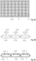
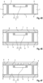
- Fig. 4 comprises Fig. 4A to 4G and shows perspective views and cross-sectional side views for illustrating an example of a method according to the second aspect for fabricating an electronic device module according to the first aspect.
- Fig. 4A shows a top view on an array of interconnected die carriers, the array comprising a plurality of die carriers connected together in the form of a matrix.
- Each one of the die carriers may be comprised of a leadframe 2.1 as was shown in Fig. 1 .
- each one of the leadframes 2.1 is comprised of a piece of metal like copper, the piece of metal comprising an opening in which a semiconductor die is to be disposed.
- Fig. 4B shows a cross-sectional view through a portion of the leadframe array, the portion indicated by line B-B in Fig. 2A .
- Fig. 4B illustrates the insertion of semiconductor dies 2.2 into the openings of the leadframes 2.1.
- single semiconductor dies 2.2 are inserted into the openings of the leadframes 2.1. It is however also possible to dispose more complex arrangements of semiconductor dies in the openings like, for example, half bridges of two interconnected semiconductor dies.
- the semiconductor dies 2.1 can be fixed to the bottom of the openings by a soldering process.
- Fig. 4C shows the semiconductor devices 2 after coating with an adhesion promoter layer 3, in particular in the form of an Al 2 O 3 layer 3.
- an Al 2 O 3 layer 3 can be produced as shown in Fig. 2A .
- a layer stack consisting of a lower Al 2 O 3 layer and an upper AlOOH layer, as shown in Fig. 2B can be produced from this by dipping the leadframe array with the Al 2 O 3 layer into a bath of hot deionized water, as was already described above.
- the leadframe array of interconnected semiconductor devices 2 is singulated into a plurality of individual semiconductor devices 2 each one of which being covered with an adhesion promoter layer 3.
- Fig. 4D shows one of the semiconductor devices 2 after inserting it into an opening 1A of a core layer 1.
- the core layer 1 comprises an FR4 material.
- FR1, FR2, FR3, or, a BT-epoxy where BT stands for bismaleimidtriazine
- a polyimide a polyimide
- a cyanate ester glass
- ceramic AlO, SiN
- electrically conductive materials are conceivable as materials of the core layer 1.
- the core layer 1 is covered by a further adhesion promoter layer 8 which may be produced in the same way as the adhesion promoter layer 3 of the semiconductor device 2.
- the adhesion promoter layer 8 of the core layer 1 can thus also have either a singular layer of Al 2 O 3 or a layer stack consisting of a lower Al 2 O 3 layer and an upper AlOOH layer.
- Fig. 4E shows the semiconductor device 2 of Fig. 4D after applying prepreg layers 4 and 5 on upper and lower surfaces of the semiconductor device 2 and the core layer 1.
- Each one of the prepreg layers 4 and 5 comprises a copper layer 6 and 7 on an outer surface thereof, respectively.
- the prepreg layers 4 and 5 and the core layer 1 are pressed together and material of the prepreg layers 4 and 5 is flowing into intermediate spaces between the semiconductor device 2 and inner walls of the opening 1A so that upper and lower prepreg layers 4 and 5 are connected with each other.
- Fig. 4F shows the semiconductor device module after drilling vias into the upper copper layer 7 and the upper portion of the laminated prepreg layer 4, part of the vias reaching down to the contact pads of the semiconductor die 2.2 and to the leadframe 2.1.
- one of the vias extends down to the source pad, another one down to the gate pad, another one down to the source sense pad, if present, and another one down to the leadframe 2.1 which is electrically connected with the drain pad of the semiconductor die 2.2, the drain pad being located on a lower main face of the semiconductor die 2.2.
- Each one of the vias is then filled with copper by chemical galvanic plating and connected with an area or trace of the upper copper layer 7.
- the present disclosure is also related to a module and a method for fabricating the same, the module comprising a core layer, an adhesion promoter layer covering the core layer and an encapsulant layer embedding the core layer.
- the module comprising a core layer, an adhesion promoter layer covering the core layer and an encapsulant layer embedding the core layer.
- an adhesion promoter layer in, for example, a PCB or other substrates, independent of the implementation of electrical or electronic components in the PCB.
- Example 1 is an electronic device module, comprising a core layer comprising an opening, an electronic device disposed in the opening, one or both of the core layer and the electronic device being at least partially covered by an adhesion promoter layer, and an encapsulant layer embedding the core layer and the electronic device.
- Example 2 is the semiconductor package according to Example 1, wherein the adhesion promoter layer comprises an Al 2 O 3 layer.
- Example 3 is the semiconductor package according to Example 1 or 2, wherein the adhesion promoter layer comprises a first layer of Al 2 O 3 and a second layer of AlOOH disposed on the first layer.
- Example 4 is the semiconductor package according to any one of the preceding Examples, wherein the core layer is covered by a further adhesion promoter layer.
- Example 5 is a method for fabricating an electronic device module, the method comprising providing a core layer comprising an opening, providing an electronic device, depositing an adhesion promoter layer at least partially on one or both of the core layer and the electronic device, placing the electronic device in the opening, and embedding the electronic device and the core layer at least partially by an encapsulant layer.
- Example 6 is the method according to Example 5, wherein the electronic device is placed in the opening and thereafter the adhesion promoter layer is deposited at least partially on both the core layer and the electronic device.
- Example 7 is the method according to Example 5 or 6, further comprising depositing the first adhesion promoter layer by atomic layer deposition.
- Example 8 is the method according to any one of Examples 5 to 7, wherein the adhesion promoter layer comprises an Al 2 O 3 layer.
- Example 9 is the method according to any one of Examples 5 to 8, wherein depositing the adhesion promoter layer comprises depositing a first layer of Al 2 O 3 and depositing a second layer of AlOOH on the first layer.
- Example 10 is the method according to any one of Examples 5 to 9, wherein the core layer is covered by a further adhesion promoter layer.
- Example 11 is a device module, comprising a core layer, the core layer being at least partially covered by an adhesion promoter layer, and an encapsulant layer embedding the core layer.
- Example 12 is the semiconductor package according to Example 11, wherein the adhesion promoter layer comprises an Al 2 O 3 layer.
- Example 13 is the semiconductor package according to Example 11 or 12, wherein the adhesion promoter layer comprises a first layer of Al 2 O 3 and a second layer of AlOOH disposed on the first layer.
- Example 14 is the device module according to any one of Examples 11 to 13, further comprising the core layer comprising an opening, and an electronic device disposed in the opening.
- Example 15 is a method for fabricating a device module, the method comprising providing a core layer, depositing an adhesion promoter layer at least partially on the core layer, embedding the core layer in an encapsulant layer.
- Example 16 is the method according to Example 15, further comprising depositing the first adhesion promoter layer by atomic layer deposition.
- Example 17 is the method according to Example 15 or 16, wherein the adhesion promoter layer comprises an Al 2 O 3 layer.
- Example 18 is the method according to any one of Examples 15 to 17, wherein depositing the adhesion promoter layer comprises depositing a first layer of Al 2 O 3 and depositing a second layer of AlOOH on the first layer.
- Example 19 is the semiconductor package according any one of Examples 15 to 18, further comprising the core layer comprising an opening, and disposing an electronic device in the opening.
Landscapes
- Structures Or Materials For Encapsulating Or Coating Semiconductor Devices Or Solid State Devices (AREA)
- Chemical & Material Sciences (AREA)
- Engineering & Computer Science (AREA)
- Ceramic Engineering (AREA)
Abstract
Description
- The present disclosure is related to an electronic device module, a method for fabricating an electronic device module, a device module, and a method for fabricating a device module.
- Over the last couple of years a lot of activities have been carried out concerning the embedding of passive components and active semiconductor dies into PCB or package carrier systems. Some low voltage use cases have found their way into production as embedding provides additional value compared to module or discrete packaging solutions, such as compactness (power density), short lead lengths leading to remarkably low parasitic inductances, good thermal management and significantly improved power cycling capability. These benefits are also seen to be attractive for power applications with high voltages up to 1200 V and specially for fast switching applications > 20 kHz. Nevertheless, some existing blocking points, when looking at how chip embedding is done today, have to be solved first as in the future peak voltages of 1700V, 2000V or even higher are under consideration.
- The current chip embedding process does not fulfil high voltage application requirements. The breakdown voltage, ion impurity level (sodium, chlorine, etc.) and the overall reliability of current PCB materials that are used for chip embedding are limited for 650 V (or even below) devices. One of the further problems is also the limited adhesion of polymer layers like prepreg layers and to the core layer of the PCB and possible local delamination of these layers from each other, and in the presence of a device like a semiconductor device also the delamination of the prepreg layers from the semiconductor device.
- For these and other reasons there is a need for the present disclosure.
- A first aspect of the present disclosure is related to an electronic device module comprising a core layer comprising an opening, an electronic device disposed in the opening, one or both of the core layer and the electronic device being at least partially covered by an adhesion promoter layer, and an encapsulant layer at least partially embedding the core layer and the electronic device.
- A second aspect of the present disclosure is related to a method for fabricating an electronic device module, the method comprising providing a core layer comprising an opening, providing an electronic device, depositing an adhesion promoter layer at least partially on one or both of the core layer and the electronic device, placing the electronic device in the opening, and at least partially embedding the electronic device and the core layer by an encapsulant layer.
- A third aspect of the present disclosure is related to a module comprising a core layer, the core layer being at least partially covered by an adhesion promoter layer, and an encapsulant layer at least partially embedding the core layer.
- A forth aspect of the present disclosure is related to a method for fabricating a module, the method comprising providing a core layer, depositing an adhesion promoter layer at least partially on the core layer, embedding at least partially the core layer with an encapsulant layer.
- The accompanying drawings are included to provide a further understanding of embodiments and are incorporated in and constitute a part of this specification. The drawings illustrate embodiments and together with the description serve to explain principles of embodiments. Other embodiments and many of the intended advantages of embodiments will be readily appreciated as they become better understood by reference to the following detailed description.
- The elements of the drawings are not necessarily to scale relative to each other. Like reference numerals designate corresponding similar parts.
-
Fig. 1 shows an example of an electronic device module according to the first aspect. -
Fig. 2 comprisesFig. 2A and 2B and shows cross-sectional side views of a first example of an adhesion promoter layer comprising a single Al2O3 layer (A), and a second example of an adhesion promoter layer comprising a layer stack of an Al2O3 layer and an AlOOH layer (B). -
Fig. 3 shows a flow diagram of a method according to the second aspect for fabricating an electronic device module according to the first aspect. -
Fig. 4 comprisesFig. 4A to 4F and shows perspective views and cross-sectional side views for illustrating an example of a method according to the second aspect for fabricating an electronic device module according to the first aspect. - In the following detailed description, reference is made to the accompanying drawings, which form a part hereof, and in which is shown by way of illustration specific embodiments in which the disclosure may be practiced. In this regard, directional terminology, such as "top", "bottom", "front", "back", "leading", "trailing", etc., is used with reference to the orientation of the Figure(s) being described. Because components of embodiments can be positioned in a number of different orientations, the directional terminology is used for purposes of illustration and is in no way limiting. It is to be understood that other embodiments may be utilized and structural or logical changes may be made without departing from the scope of the present disclosure. The following detailed description, therefore, is not to be taken in a limiting sense, and the scope of the present disclosure is defined by the appended claims.
- It is to be understood that the features of the various exemplary embodiments described herein may be combined with each other, unless specifically noted otherwise.
- As employed in this specification, the terms "bonded", "attached", "connected", "coupled" and/or "electrically connected/electrically coupled" are not meant to mean that the elements or layers must directly be contacted together; intervening elements or layers may be provided between the "bonded", "attached", "connected", "coupled" and/or "electrically connected/electrically coupled" elements, respectively. However, in accordance with the disclosure, the above-mentioned terms may, optionally, also have the specific meaning that the elements or layers are directly contacted together, i.e. that no intervening elements or layers are provided between the "bonded", "attached", "connected", "coupled" and/or "electrically connected/electrically coupled" elements, respectively.
- Further, the word "over" used with regard to a part, element or material layer formed or located "over" a surface may be used herein to mean that the part, element or material layer be located (e.g. placed, formed, deposited, etc.) "indirectly on" the implied surface with one or more additional parts, elements or layers being arranged between the implied surface and the part, element or material layer. However, the word "over" used with regard to a part, element or material layer formed or located "over" a surface may, optionally, also have the specific meaning that the part, element or material layer be located (e.g. placed, formed, deposited, etc.) "directly on", e.g. in direct contact with, the implied surface.
-
Fig. 1 shows an example of an electronic device module according to the first aspect. - More specifically,
Fig. 1 shows anelectronic device module 10 comprising acore layer 1 comprising anopening 1A, and anelectronic device 2 disposed in the opening. Thecore layer 1 and theelectronic device 2 are embedded in anencapsulant layer 4 such that thecore layer 1 and theelectronic device 2 are disposed on a lower horizontal layer of theencapsulant layer 4, an upper horizontal layer of thepolymer layer 4 is disposed on upper surfaces of thecore layer 1 and theelectronic device 2, and vertical layers of theencapsulant layer 4 are filled in intermediate spaces between side walls of thecore layer 1 and side walls of theelectronic device 2 within the opening 1A of thecore layer 1. - The
core layer 1 can, for example, comprise an FR1, FR2, FR3, or FR4 material, a BT-Epoxy (where BT stands for bismaleimidtriazine), a polyimide, or a cyanate ester. Theencapsulant layer 4 may comprise a polymer layer and in particular aprepreg layer 4. Afirst Cu layer 6 may be disposed on a rear surface of theencapsulant layer 4 remote from thecore layer 1. And asecond copper layer 7 may be disposed on an upper surface of the upper layer of theencapsulant layer 4, thesecond copper layer 7 comprising separate electrical areas or traces, the electrical areas connected with electrical vias being connected with contacts pads of theelectronic device 2. - The
electronic device 2 may in particular comprise a die carrier 2.1, and a semiconductor die 2.2 attached to the die carrier 2.1. The die carrier 2.1 can be a leadframe or any other kind of substrate like a DCB (direct copper bond), an AMB (active metal braze or an IMS (insulated metal substrate). Thesemiconductor device 2 may also comprise two or more semiconductor dies which may be interconnected to form, e.g., a half bridge, the half bridge being disposed in the opening. - The semiconductor die 2.2 may comprise a semiconductor transistor die 2.2 like, e.g. one or more of an IGBT, a MOSFET die, a CoolMOS, or a wide band gap semiconductor transistor like SiC-MOS, or GaN-MOS. The semiconductor transistor die 2.2 may comprise a contact pad 2.2A on an upper surface thereof, which contact pad 2.2A can be, for example, a source pad 2A.
- It should be mentioned that the semiconductor device can also have a completely different structure. While the
semiconductor component 2 ofFig. 1 is electrically conductive on its main surfaces, another semiconductor component may also be designed to be partially or completely electrically insulating, in particular on the front and/or rear side the semiconductor component may be designed to be at least partially electrically insulating. In particular, the semiconductor component can be completely embedded in an encapsulant which can be thermally conductive, e.g. in case of a fullpack. - At this point it should be mentioned here that instead of a semiconductor device, another component can also be installed in the module in the manner described. For example, a passive component such as a diode, a capacitor or a resistor can be used. Also a heat sink in the form of a copper insert can be used. A conductor rail or bus bar is also conceivable for use.
- The
electronic device 2 is covered by anadhesion promoter layer 3 and thecore layer 1 may also be covered by a furtheradhesion promoter layer 8. Theadhesion promoter layer 3 and the furtheradhesion promoter layer 8 can be formed in an identical manner or they can be formed different. In both cases the adhesion promoter layer can be formed by a single e.g. homogeneous layer, e.g. of Al2O3, or by a layer stack of e.g. two layers, e.g. of a lower layer of Al2O3, and an upper layer e.g. of AlOOH formed by the conversion of Al2O3 which will be explained later. Theelectronic device 2 can be completely or partially covered by theadhesion promoter layer 3 and thecore layer 1 can be completely or partially covered by the furtheradhesion promoter layer 8. -
Fig. 2 comprisesFig. 2A and 2B and shows cross-sectional side views of a first example of an adhesion promoter layer comprising a single Al2O3 layer (A), and a second example of an adhesion promoter layer comprising a layer stack of an Al2O3 layer and an AlOOH layer (B). -
Fig. 2A shows asubstrate 12 and a single Al2O3 layer 13 disposed on thesubstrate 12. Thesubstrate 12 can be of any kind, depending on the form and structure of the semiconductor device or the core layer used. In case of the example as shown inFig. 1 , thesubstrate 12 would be a leadframe. On the other hand it could also be the case that the semiconductor device comprises a semiconductor package in which a semiconductor die is fully or almost fully encapsulated by a compound like a molded compound so that the latter would form thesubstrate 12. - The Al2O3 layer 13 can be, for example, deposited by atomic layer deposition (ALD). ALD is a thin-film deposition technique based on the sequential use of a gasphase chemical process. It is a subclass of chemical vapour deposition. The majority of ALD reactions use two chemicals called precursors (also called "reactants"). These precursors react with the surface of a material one at a time in a sequential, self-limiting, manner. The precursors only react with the surface molecules, but not with themselves. A thin and
dense layer 13 of Al2O3 can in this way be slowly deposited through repeated exposure to separate precursors. - For depositing the Al2O3 layer 13 by ALD the applied temperature is typically in a range from 100°C to 350°C. The deposition takes place in cycles in which a precursor A and a precursor B are alternately deposited on the substrate and rinsing with nitrogen takes place in between. One atomic or molecular layer is deposited in each cycle. In the present case of the deposition of Al2O3, a layer with a thickness of 20 nm is deposited after 200 cycles. The layer thickness can be in a range from 3 nm to 100 nm.
-
Fig. 2B shows asubstrate 22 and an adhesion promoter layer comprising alayer stack 23 comprising a first layer 23.1 of Al2O3 and a second layer 23.2 of AlOOH. The same applies to thesubstrate 22 as described above for thesubstrate 12 ofFig. 2A . The first layer 23.1 of Al2O3 can be obtained by ALD as was described above in connection withFig. 2A . Afterwards a following dip into hot deionized water at least partially transfers the dense Al2O3 layer into a dendritic AlOOH layer.. -
Fig. 3 shows a flow diagram of a method according to the second aspect for fabricating an electronic device module according to the first aspect. - More specifically, the
method 100 comprises providing a core layer comprising an opening (110), providing an electronic device (120), depositing an adhesion promoter layer on the electronic device (130), placing the electronic device in the opening (140), and at least partially embedding the electronic device and the core layer in an encapsulant layer (150). - According to further examples, as already described in connection with the previous
Figures 1 and 2 , the method may further comprise one or more of depositing the adhesion promoter layer by atomic layer deposition, the adhesion promoter layer comprising an Al2O3 layer either as a single layer or as part of a layer stack together with an AlOOH layer, in particular by depositing the adhesion promoter layer comprising depositing a first layer of Al2O3 and converting said first layer partially into a rough AlOOH layer by hydrothermal conversion. - It is also worth mentioning that the
individual steps 110 to 150 can also be carried out in a sequence other than that indicated above. In particular, the deposition of the adhesion promoter layer can also take place after the semiconductor device has been placed in the opening, in which case the core layer will inevitably also be covered with the adhesion promoter layer. -
Fig. 4 comprisesFig. 4A to 4G and shows perspective views and cross-sectional side views for illustrating an example of a method according to the second aspect for fabricating an electronic device module according to the first aspect. -
Fig. 4A shows a top view on an array of interconnected die carriers, the array comprising a plurality of die carriers connected together in the form of a matrix. Each one of the die carriers may be comprised of a leadframe 2.1 as was shown inFig. 1 . In this Example each one of the leadframes 2.1 is comprised of a piece of metal like copper, the piece of metal comprising an opening in which a semiconductor die is to be disposed. -
Fig. 4B shows a cross-sectional view through a portion of the leadframe array, the portion indicated by line B-B inFig. 2A .Fig. 4B illustrates the insertion of semiconductor dies 2.2 into the openings of the leadframes 2.1. In this Example single semiconductor dies 2.2 are inserted into the openings of the leadframes 2.1. It is however also possible to dispose more complex arrangements of semiconductor dies in the openings like, for example, half bridges of two interconnected semiconductor dies. The semiconductor dies 2.1 can be fixed to the bottom of the openings by a soldering process. -
Fig. 4C shows thesemiconductor devices 2 after coating with anadhesion promoter layer 3, in particular in the form of an Al2O3 layer 3. - In this way, an Al2O3 layer 3 can be produced as shown in
Fig. 2A . If desired, a layer stack consisting of a lower Al2O3 layer and an upper AlOOH layer, as shown inFig. 2B , can be produced from this by dipping the leadframe array with the Al2O3 layer into a bath of hot deionized water, as was already described above. - Afterwards the leadframe array of
interconnected semiconductor devices 2 is singulated into a plurality ofindividual semiconductor devices 2 each one of which being covered with anadhesion promoter layer 3. -
Fig. 4D shows one of thesemiconductor devices 2 after inserting it into anopening 1A of acore layer 1. In the present Example thecore layer 1 comprises an FR4 material. However, also other materials like FR1, FR2, FR3, or, a BT-epoxy (where BT stands for bismaleimidtriazine), a polyimide, a cyanate ester, glass, ceramic (AlO, SiN), and also electrically conductive materials, are conceivable as materials of thecore layer 1. In the present Example thecore layer 1 is covered by a furtheradhesion promoter layer 8 which may be produced in the same way as theadhesion promoter layer 3 of thesemiconductor device 2. Theadhesion promoter layer 8 of thecore layer 1 can thus also have either a singular layer of Al2O3 or a layer stack consisting of a lower Al2O3 layer and an upper AlOOH layer. -
Fig. 4E shows thesemiconductor device 2 ofFig. 4D after applyingprepreg layers 4 and 5 on upper and lower surfaces of thesemiconductor device 2 and thecore layer 1. Each one of the prepreg layers 4 and 5 comprises acopper layer core layer 1 are pressed together and material of the prepreg layers 4 and 5 is flowing into intermediate spaces between thesemiconductor device 2 and inner walls of theopening 1A so that upper andlower prepreg layers 4 and 5 are connected with each other. -
Fig. 4F shows the semiconductor device module after drilling vias into theupper copper layer 7 and the upper portion of thelaminated prepreg layer 4, part of the vias reaching down to the contact pads of the semiconductor die 2.2 and to the leadframe 2.1. For example, one of the vias extends down to the source pad, another one down to the gate pad, another one down to the source sense pad, if present, and another one down to the leadframe 2.1 which is electrically connected with the drain pad of the semiconductor die 2.2, the drain pad being located on a lower main face of the semiconductor die 2.2. Each one of the vias is then filled with copper by chemical galvanic plating and connected with an area or trace of theupper copper layer 7. - According to the third and fourth aspects, the present disclosure is also related to a module and a method for fabricating the same, the module comprising a core layer, an adhesion promoter layer covering the core layer and an encapsulant layer embedding the core layer. This means in other words, the use of an adhesion promoter layer in, for example, a PCB or other substrates, independent of the implementation of electrical or electronic components in the PCB. The same properties and features of the individual components as well as of the manufacturing processes as described above in connection with the first and second aspects can be used.
- In the following specific examples of the present disclosure are described.
- Example 1 is an electronic device module, comprising a core layer comprising an opening, an electronic device disposed in the opening, one or both of the core layer and the electronic device being at least partially covered by an adhesion promoter layer, and an encapsulant layer embedding the core layer and the electronic device.
- Example 2 is the semiconductor package according to Example 1, wherein the adhesion promoter layer comprises an Al2O3 layer.
- Example 3 is the semiconductor package according to Example 1 or 2, wherein the adhesion promoter layer comprises a first layer of Al2O3 and a second layer of AlOOH disposed on the first layer.
- Example 4 is the semiconductor package according to any one of the preceding Examples, wherein the core layer is covered by a further adhesion promoter layer.
- Example 5 is a method for fabricating an electronic device module, the method comprising providing a core layer comprising an opening, providing an electronic device, depositing an adhesion promoter layer at least partially on one or both of the core layer and the electronic device, placing the electronic device in the opening, and embedding the electronic device and the core layer at least partially by an encapsulant layer.
- Example 6 is the method according to Example 5, wherein the electronic device is placed in the opening and thereafter the adhesion promoter layer is deposited at least partially on both the core layer and the electronic device.
- Example 7 is the method according to Example 5 or 6, further comprising depositing the first adhesion promoter layer by atomic layer deposition.
- Example 8 is the method according to any one of Examples 5 to 7, wherein the adhesion promoter layer comprises an Al2O3 layer.
- Example 9 is the method according to any one of Examples 5 to 8, wherein depositing the adhesion promoter layer comprises depositing a first layer of Al2O3 and depositing a second layer of AlOOH on the first layer.
- Example 10 is the method according to any one of Examples 5 to 9, wherein the core layer is covered by a further adhesion promoter layer.
- Example 11 is a device module, comprising a core layer, the core layer being at least partially covered by an adhesion promoter layer, and an encapsulant layer embedding the core layer.
- Example 12 is the semiconductor package according to Example 11, wherein the adhesion promoter layer comprises an Al2O3 layer.
- Example 13 is the semiconductor package according to Example 11 or 12, wherein the adhesion promoter layer comprises a first layer of Al2O3 and a second layer of AlOOH disposed on the first layer.
- Example 14 is the device module according to any one of Examples 11 to 13, further comprising the core layer comprising an opening, and an electronic device disposed in the opening.
- Example 15 is a method for fabricating a device module, the method comprising providing a core layer, depositing an adhesion promoter layer at least partially on the core layer, embedding the core layer in an encapsulant layer.
- Example 16 is the method according to Example 15, further comprising depositing the first adhesion promoter layer by atomic layer deposition.
- Example 17 is the method according to Example 15 or 16, wherein the adhesion promoter layer comprises an Al2O3 layer.
- Example 18 is the method according to any one of Examples 15 to 17, wherein depositing the adhesion promoter layer comprises depositing a first layer of Al2O3 and depositing a second layer of AlOOH on the first layer.
- Example 19 is the semiconductor package according any one of Examples 15 to 18, further comprising the core layer comprising an opening, and disposing an electronic device in the opening.
- In addition, while a particular feature or aspect of an embodiment of the disclosure may have been disclosed with respect to only one of several implementations, such feature or aspect may be combined with one or more other features or aspects of the other implementations as may be desired and advantageous for any given or particular application. Furthermore, to the extent that the terms "include", "have", "with", or other variants thereof are used in either the detailed description or the claims, such terms are intended to be inclusive in a manner similar to the term "comprise". Furthermore, it should be understood that embodiments of the disclosure may be implemented in discrete circuits, partially integrated circuits or fully integrated circuits or programming means. Also, the term "exemplary" is merely meant as an example, rather than the best or optimal. It is also to be appreciated that features and/or elements depicted herein are illustrated with particular dimensions relative to one another for purposes of simplicity and ease of understanding, and that actual dimensions may differ substantially from that illustrated herein.
- Although specific embodiments have been illustrated and described herein, it will be appreciated by those of ordinary skill in the art that a variety of alternate and/or equivalent implementations may be substituted for the specific embodiments shown and described without departing from the scope of the present disclosure. This application is intended to cover any adaptations or variations of the specific embodiments discussed herein. Therefore, it is intended that this disclosure be limited only by the claims and the equivalents thereof.
Claims (19)
- An electronic device module (10), comprisinga core layer (1) comprising an opening (1A);an electronic device (2) disposed in the opening (1A), one or both of the core layer (1) and the electronic device (2) being at least partially covered by an adhesion promoter layer (3); andan encapsulant layer (4) embedding the core layer (1) and the electronic device (2).
- The electronic device module (10) according to claim 1, wherein
the adhesion promoter layer (3) comprises an Al2O3 layer. - The electronic device module (10) according to claim 1 or 2, wherein
the adhesion promoter layer (3) comprises a first layer of Al2O3 and a second layer of AlOOH disposed on the first layer. - The electronic device module (10) according to any one of the preceding claims, wherein
the core layer (1) is covered by a further adhesion promoter layer. - A method (100) for fabricating an electronic device module, the method comprising- providing a core layer comprising an opening (110);- providing an electronic device (120);- depositing an adhesion promoter layer at least partially on one or both of the core layer and the electronic device (130) ;- placing the electronic device in the opening (140); and- embedding the electronic device and the core layer at least partially by an encapsulant layer (150).
- The method according to claim 5, wherein
the electronic device is placed in the opening and thereafter the adhesion promoter layer is deposited at least partially on both the core layer and the electronic device. - The method according to claim 5 or 6, further comprising depositing the first adhesion promoter layer by atomic layer deposition.
- The method according to any one of claims 5 to 7, wherein the adhesion promoter layer (3) comprises an Al2O3 layer.
- The method according to any one of claims 5 to 8, wherein depositing the adhesion promoter layer comprises depositing a first layer of Al2O3 and depositing a second layer of AlOOH on the first layer.
- The method according to any one of claims 5 to 9, wherein the core layer (1) is covered by a further adhesion promoter layer.
- A device module, comprisinga core layer, the core layer being at least partially covered by an adhesion promoter layer; andan encapsulant layer embedding the core layer.
- The device module according to claim 11, wherein
the adhesion promoter layer (3) comprises an Al2O3 layer. - The device module according to claim 11 or 12, wherein the adhesion promoter layer comprises a first layer of Al2O3 and a second layer of AlOOH disposed on the first layer.
- The device module according to any one of claims 11 to 13, further comprisingthe core layer comprising an opening; andan electronic device disposed in the opening.
- A method for fabricating a device module, the method comprising- providing a core layer;- depositing an adhesion promoter layer at least partially on the core layer;- embedding the core layer in an encapsulant layer.
- The method according to claim 15, further comprising depositing the first adhesion promoter layer by atomic layer deposition.
- The method according to claim 15 or 16, wherein
the adhesion promoter layer comprises an Al2O3 layer. - The method according to any one of claims 15 to 17,
wherein
depositing the adhesion promoter layer comprises depositing a first layer of Al2O3 and depositing a second layer of AlOOH on the first layer. - The method according to any one of claims 15 to 18, further comprising
the core layer comprising an opening; and
disposing an electronic device in the opening.
Priority Applications (3)
| Application Number | Priority Date | Filing Date | Title |
|---|---|---|---|
| EP22174324.8A EP4280276A1 (en) | 2022-05-19 | 2022-05-19 | An electronic device module and a device module both with increased reliability due to an adhesion promoter layer |
| US18/315,193 US20230378011A1 (en) | 2022-05-19 | 2023-05-10 | Electronic device module and a device module both having an adhesion promoter layer |
| CN202310561180.XA CN117096112A (en) | 2022-05-19 | 2023-05-18 | Electronic device modules and device modules both with improved reliability due to adhesion promoter layer |
Applications Claiming Priority (1)
| Application Number | Priority Date | Filing Date | Title |
|---|---|---|---|
| EP22174324.8A EP4280276A1 (en) | 2022-05-19 | 2022-05-19 | An electronic device module and a device module both with increased reliability due to an adhesion promoter layer |
Publications (1)
| Publication Number | Publication Date |
|---|---|
| EP4280276A1 true EP4280276A1 (en) | 2023-11-22 |
Family
ID=82117669
Family Applications (1)
| Application Number | Title | Priority Date | Filing Date |
|---|---|---|---|
| EP22174324.8A Pending EP4280276A1 (en) | 2022-05-19 | 2022-05-19 | An electronic device module and a device module both with increased reliability due to an adhesion promoter layer |
Country Status (3)
| Country | Link |
|---|---|
| US (1) | US20230378011A1 (en) |
| EP (1) | EP4280276A1 (en) |
| CN (1) | CN117096112A (en) |
Families Citing this family (2)
| Publication number | Priority date | Publication date | Assignee | Title |
|---|---|---|---|---|
| KR20260038810A (en) * | 2024-09-12 | 2026-03-19 | 앱솔릭스 인코포레이티드 | Packaging substrate and semiconductor package comprising the same |
| WO2026162123A1 (en) * | 2025-01-29 | 2026-08-06 | Huawei Technologies Co., Ltd. | Semiconductor arrangement and sub-arrangement with poka-yoke structures |
Citations (7)
| Publication number | Priority date | Publication date | Assignee | Title |
|---|---|---|---|---|
| EP0987760A2 (en) * | 1998-08-31 | 2000-03-22 | General Electric Company | Multimodule interconnect structure and process |
| EP1321980A1 (en) * | 2000-09-25 | 2003-06-25 | Ibiden Co., Ltd. | Semiconductor element, method of manufacturing semiconductor element, multi-layer printed circuit board, and method of manufacturing multi-layer printed circuit board |
| US20070074900A1 (en) * | 2005-10-04 | 2007-04-05 | Samsung Electro-Mechanics Co., Ltd. | Printed circuit board and manufacturing method thereof |
| US20170287880A1 (en) * | 2016-04-04 | 2017-10-05 | Infineon Technologies Ag | Electronic Device Package Having a Dielectric Layer and an Encapsulant |
| US20190252306A1 (en) * | 2018-02-12 | 2019-08-15 | Samsung Electronics Co., Ltd. | Printed circuit board and semiconductor package including the same |
| US20200043876A1 (en) * | 2018-07-31 | 2020-02-06 | Infineon Technologies Ag | Adhesion Enhancing Structures for a Package |
| EP3855487A1 (en) * | 2020-01-22 | 2021-07-28 | At&S (China) Co., Ltd. | Component carrier having component covered with ultra-thin transition layer |
-
2022
- 2022-05-19 EP EP22174324.8A patent/EP4280276A1/en active Pending
-
2023
- 2023-05-10 US US18/315,193 patent/US20230378011A1/en active Pending
- 2023-05-18 CN CN202310561180.XA patent/CN117096112A/en active Pending
Patent Citations (7)
| Publication number | Priority date | Publication date | Assignee | Title |
|---|---|---|---|---|
| EP0987760A2 (en) * | 1998-08-31 | 2000-03-22 | General Electric Company | Multimodule interconnect structure and process |
| EP1321980A1 (en) * | 2000-09-25 | 2003-06-25 | Ibiden Co., Ltd. | Semiconductor element, method of manufacturing semiconductor element, multi-layer printed circuit board, and method of manufacturing multi-layer printed circuit board |
| US20070074900A1 (en) * | 2005-10-04 | 2007-04-05 | Samsung Electro-Mechanics Co., Ltd. | Printed circuit board and manufacturing method thereof |
| US20170287880A1 (en) * | 2016-04-04 | 2017-10-05 | Infineon Technologies Ag | Electronic Device Package Having a Dielectric Layer and an Encapsulant |
| US20190252306A1 (en) * | 2018-02-12 | 2019-08-15 | Samsung Electronics Co., Ltd. | Printed circuit board and semiconductor package including the same |
| US20200043876A1 (en) * | 2018-07-31 | 2020-02-06 | Infineon Technologies Ag | Adhesion Enhancing Structures for a Package |
| EP3855487A1 (en) * | 2020-01-22 | 2021-07-28 | At&S (China) Co., Ltd. | Component carrier having component covered with ultra-thin transition layer |
Also Published As
| Publication number | Publication date |
|---|---|
| US20230378011A1 (en) | 2023-11-23 |
| CN117096112A (en) | 2023-11-21 |
Similar Documents
| Publication | Publication Date | Title |
|---|---|---|
| US7800217B2 (en) | Power semiconductor device connected in distinct layers of plastic | |
| US8084816B2 (en) | Semiconductor module | |
| US8806741B2 (en) | Method of making an electronic device | |
| US7838978B2 (en) | Semiconductor device | |
| US7846779B2 (en) | Power device package and method of fabricating the same | |
| US8410590B2 (en) | Device including a power semiconductor chip electrically coupled to a leadframe via a metallic layer | |
| US8324739B2 (en) | Semiconductor device | |
| US10079195B2 (en) | Semiconductor chip package comprising laterally extending connectors | |
| US12080669B2 (en) | Semiconductor device module having vertical metallic contacts and a method for fabricating the same | |
| US20070246808A1 (en) | Power semiconductor module having surface-mountable flat external contacts and method for producing the same | |
| US20230378011A1 (en) | Electronic device module and a device module both having an adhesion promoter layer | |
| US12463116B2 (en) | Method for fabricating a semiconductor device including an embedded semiconductor die | |
| US10573585B2 (en) | Power converter having a conductive clip | |
| US9379050B2 (en) | Electronic device | |
| US20230282591A1 (en) | Semiconductor package and a semiconductor device module including the same | |
| US20230360929A1 (en) | Method for fabricating a semiconductor device module with increased reliability and a semiconductor device module | |
| US11404392B1 (en) | Molded semiconductor module for PCB embedding |
Legal Events
| Date | Code | Title | Description |
|---|---|---|---|
| PUAI | Public reference made under article 153(3) epc to a published international application that has entered the european phase |
Free format text: ORIGINAL CODE: 0009012 |
|
| STAA | Information on the status of an ep patent application or granted ep patent |
Free format text: STATUS: THE APPLICATION HAS BEEN PUBLISHED |
|
| AK | Designated contracting states |
Kind code of ref document: A1 Designated state(s): AL AT BE BG CH CY CZ DE DK EE ES FI FR GB GR HR HU IE IS IT LI LT LU LV MC MK MT NL NO PL PT RO RS SE SI SK SM TR |
|
| STAA | Information on the status of an ep patent application or granted ep patent |
Free format text: STATUS: REQUEST FOR EXAMINATION WAS MADE |
|
| 17P | Request for examination filed |
Effective date: 20240513 |
|
| RBV | Designated contracting states (corrected) |
Designated state(s): AL AT BE BG CH CY CZ DE DK EE ES FI FR GB GR HR HU IE IS IT LI LT LU LV MC MK MT NL NO PL PT RO RS SE SI SK SM TR |