EP4279290A1 - Information page - Google Patents
Information page Download PDFInfo
- Publication number
- EP4279290A1 EP4279290A1 EP23200302.0A EP23200302A EP4279290A1 EP 4279290 A1 EP4279290 A1 EP 4279290A1 EP 23200302 A EP23200302 A EP 23200302A EP 4279290 A1 EP4279290 A1 EP 4279290A1
- Authority
- EP
- European Patent Office
- Prior art keywords
- layer
- module
- information page
- security document
- chip
- Prior art date
- Legal status (The legal status is an assumption and is not a legal conclusion. Google has not performed a legal analysis and makes no representation as to the accuracy of the status listed.)
- Granted
Links
Images

Classifications
-
- B—PERFORMING OPERATIONS; TRANSPORTING
- B42—BOOKBINDING; ALBUMS; FILES; SPECIAL PRINTED MATTER
- B42D—BOOKS; BOOK COVERS; LOOSE LEAVES; PRINTED MATTER CHARACTERISED BY IDENTIFICATION OR SECURITY FEATURES; PRINTED MATTER OF SPECIAL FORMAT OR STYLE NOT OTHERWISE PROVIDED FOR; DEVICES FOR USE THEREWITH AND NOT OTHERWISE PROVIDED FOR; MOVABLE-STRIP WRITING OR READING APPARATUS
- B42D25/00—Information-bearing cards or sheet-like structures characterised by identification or security features; Manufacture thereof
- B42D25/20—Information-bearing cards or sheet-like structures characterised by identification or security features; Manufacture thereof characterised by a particular use or purpose
- B42D25/22—Information-bearing cards or sheet-like structures characterised by identification or security features; Manufacture thereof characterised by a particular use or purpose for use in combination with accessories specially adapted for information-bearing cards
-
- B—PERFORMING OPERATIONS; TRANSPORTING
- B42—BOOKBINDING; ALBUMS; FILES; SPECIAL PRINTED MATTER
- B42D—BOOKS; BOOK COVERS; LOOSE LEAVES; PRINTED MATTER CHARACTERISED BY IDENTIFICATION OR SECURITY FEATURES; PRINTED MATTER OF SPECIAL FORMAT OR STYLE NOT OTHERWISE PROVIDED FOR; DEVICES FOR USE THEREWITH AND NOT OTHERWISE PROVIDED FOR; MOVABLE-STRIP WRITING OR READING APPARATUS
- B42D25/00—Information-bearing cards or sheet-like structures characterised by identification or security features; Manufacture thereof
- B42D25/30—Identification or security features, e.g. for preventing forgery
- B42D25/351—Translucent or partly translucent parts, e.g. windows
-
- B—PERFORMING OPERATIONS; TRANSPORTING
- B42—BOOKBINDING; ALBUMS; FILES; SPECIAL PRINTED MATTER
- B42D—BOOKS; BOOK COVERS; LOOSE LEAVES; PRINTED MATTER CHARACTERISED BY IDENTIFICATION OR SECURITY FEATURES; PRINTED MATTER OF SPECIAL FORMAT OR STYLE NOT OTHERWISE PROVIDED FOR; DEVICES FOR USE THEREWITH AND NOT OTHERWISE PROVIDED FOR; MOVABLE-STRIP WRITING OR READING APPARATUS
- B42D25/00—Information-bearing cards or sheet-like structures characterised by identification or security features; Manufacture thereof
- B42D25/20—Information-bearing cards or sheet-like structures characterised by identification or security features; Manufacture thereof characterised by a particular use or purpose
- B42D25/24—Passports
-
- B—PERFORMING OPERATIONS; TRANSPORTING
- B42—BOOKBINDING; ALBUMS; FILES; SPECIAL PRINTED MATTER
- B42D—BOOKS; BOOK COVERS; LOOSE LEAVES; PRINTED MATTER CHARACTERISED BY IDENTIFICATION OR SECURITY FEATURES; PRINTED MATTER OF SPECIAL FORMAT OR STYLE NOT OTHERWISE PROVIDED FOR; DEVICES FOR USE THEREWITH AND NOT OTHERWISE PROVIDED FOR; MOVABLE-STRIP WRITING OR READING APPARATUS
- B42D25/00—Information-bearing cards or sheet-like structures characterised by identification or security features; Manufacture thereof
- B42D25/20—Information-bearing cards or sheet-like structures characterised by identification or security features; Manufacture thereof characterised by a particular use or purpose
- B42D25/29—Securities; Bank notes
-
- B—PERFORMING OPERATIONS; TRANSPORTING
- B42—BOOKBINDING; ALBUMS; FILES; SPECIAL PRINTED MATTER
- B42D—BOOKS; BOOK COVERS; LOOSE LEAVES; PRINTED MATTER CHARACTERISED BY IDENTIFICATION OR SECURITY FEATURES; PRINTED MATTER OF SPECIAL FORMAT OR STYLE NOT OTHERWISE PROVIDED FOR; DEVICES FOR USE THEREWITH AND NOT OTHERWISE PROVIDED FOR; MOVABLE-STRIP WRITING OR READING APPARATUS
- B42D25/00—Information-bearing cards or sheet-like structures characterised by identification or security features; Manufacture thereof
- B42D25/30—Identification or security features, e.g. for preventing forgery
- B42D25/305—Associated digital information
-
- B—PERFORMING OPERATIONS; TRANSPORTING
- B42—BOOKBINDING; ALBUMS; FILES; SPECIAL PRINTED MATTER
- B42D—BOOKS; BOOK COVERS; LOOSE LEAVES; PRINTED MATTER CHARACTERISED BY IDENTIFICATION OR SECURITY FEATURES; PRINTED MATTER OF SPECIAL FORMAT OR STYLE NOT OTHERWISE PROVIDED FOR; DEVICES FOR USE THEREWITH AND NOT OTHERWISE PROVIDED FOR; MOVABLE-STRIP WRITING OR READING APPARATUS
- B42D25/00—Information-bearing cards or sheet-like structures characterised by identification or security features; Manufacture thereof
- B42D25/30—Identification or security features, e.g. for preventing forgery
- B42D25/328—Diffraction gratings; Holograms
-
- B—PERFORMING OPERATIONS; TRANSPORTING
- B42—BOOKBINDING; ALBUMS; FILES; SPECIAL PRINTED MATTER
- B42D—BOOKS; BOOK COVERS; LOOSE LEAVES; PRINTED MATTER CHARACTERISED BY IDENTIFICATION OR SECURITY FEATURES; PRINTED MATTER OF SPECIAL FORMAT OR STYLE NOT OTHERWISE PROVIDED FOR; DEVICES FOR USE THEREWITH AND NOT OTHERWISE PROVIDED FOR; MOVABLE-STRIP WRITING OR READING APPARATUS
- B42D25/00—Information-bearing cards or sheet-like structures characterised by identification or security features; Manufacture thereof
- B42D25/40—Manufacture
- B42D25/405—Marking
- B42D25/41—Marking using electromagnetic radiation
-
- B—PERFORMING OPERATIONS; TRANSPORTING
- B42—BOOKBINDING; ALBUMS; FILES; SPECIAL PRINTED MATTER
- B42D—BOOKS; BOOK COVERS; LOOSE LEAVES; PRINTED MATTER CHARACTERISED BY IDENTIFICATION OR SECURITY FEATURES; PRINTED MATTER OF SPECIAL FORMAT OR STYLE NOT OTHERWISE PROVIDED FOR; DEVICES FOR USE THEREWITH AND NOT OTHERWISE PROVIDED FOR; MOVABLE-STRIP WRITING OR READING APPARATUS
- B42D25/00—Information-bearing cards or sheet-like structures characterised by identification or security features; Manufacture thereof
- B42D25/40—Manufacture
- B42D25/45—Associating two or more layers
-
- G—PHYSICS
- G06—COMPUTING OR CALCULATING; COUNTING
- G06K—GRAPHICAL DATA READING; PRESENTATION OF DATA; RECORD CARRIERS; HANDLING RECORD CARRIERS
- G06K19/00—Record carriers for use with machines and with at least a part designed to carry digital markings
- G06K19/02—Record carriers for use with machines and with at least a part designed to carry digital markings characterised by the selection of materials, e.g. to avoid wear during transport through the machine
-
- G—PHYSICS
- G06—COMPUTING OR CALCULATING; COUNTING
- G06K—GRAPHICAL DATA READING; PRESENTATION OF DATA; RECORD CARRIERS; HANDLING RECORD CARRIERS
- G06K19/00—Record carriers for use with machines and with at least a part designed to carry digital markings
- G06K19/06—Record carriers for use with machines and with at least a part designed to carry digital markings characterised by the kind of the digital marking, e.g. shape, nature, code
- G06K19/06009—Record carriers for use with machines and with at least a part designed to carry digital markings characterised by the kind of the digital marking, e.g. shape, nature, code with optically detectable marking
-
- G—PHYSICS
- G06—COMPUTING OR CALCULATING; COUNTING
- G06K—GRAPHICAL DATA READING; PRESENTATION OF DATA; RECORD CARRIERS; HANDLING RECORD CARRIERS
- G06K19/00—Record carriers for use with machines and with at least a part designed to carry digital markings
- G06K19/06—Record carriers for use with machines and with at least a part designed to carry digital markings characterised by the kind of the digital marking, e.g. shape, nature, code
- G06K19/067—Record carriers with conductive marks, printed circuits or semiconductor circuit elements, e.g. credit or identity cards also with resonating or responding marks without active components
- G06K19/07—Record carriers with conductive marks, printed circuits or semiconductor circuit elements, e.g. credit or identity cards also with resonating or responding marks without active components with integrated circuit chips
- G06K19/077—Constructional details, e.g. mounting of circuits in the carrier
-
- G—PHYSICS
- G06—COMPUTING OR CALCULATING; COUNTING
- G06K—GRAPHICAL DATA READING; PRESENTATION OF DATA; RECORD CARRIERS; HANDLING RECORD CARRIERS
- G06K19/00—Record carriers for use with machines and with at least a part designed to carry digital markings
- G06K19/06—Record carriers for use with machines and with at least a part designed to carry digital markings characterised by the kind of the digital marking, e.g. shape, nature, code
- G06K19/067—Record carriers with conductive marks, printed circuits or semiconductor circuit elements, e.g. credit or identity cards also with resonating or responding marks without active components
- G06K19/07—Record carriers with conductive marks, printed circuits or semiconductor circuit elements, e.g. credit or identity cards also with resonating or responding marks without active components with integrated circuit chips
- G06K19/077—Constructional details, e.g. mounting of circuits in the carrier
- G06K19/0772—Physical layout of the record carrier
Definitions
- the present invention relates to an information page of a security document having an IC module, such as a passport, and more particularly to an information page of a security document which can prevent deformation of an IC module.
- a security document such as a passport contains an information page with a built-in IC module.
- an information page with a built-in IC module has a multi-layer structure including a plurality of layers, in which the IC module is incorporated.
- Such an information page can be obtained by preparing a multi-layer structure comprised of a laminate of layers, in which an IC module is interposed, and subjecting the multi-layer structure to hot pressing.
- Such deformation of the IC module caused by the application of a non-uniform external force thereto, can affect the performance of the IC module and, in addition, is undesirable in terms of appearance.
- Patent document 1 Published Japanese Translation No. 2009-514708 of the PCT International Publication
- the present invention has been made in view of the above situation. It is therefore an object of the present invention to provide an information page of a security document in which no non-uniform external force acts on an IC module, and there is no occurrence of deformation of the IC module.
- the present invention provides an information page of a security document, comprising: a core layer having flexibility for incorporating the information page into the security document; an IC module holding layer provided on one surface of the core layer via an intermediate layer; and an IC module held in the IC module holding layer and including a substrate, and an IC chip provided on the substrate, wherein the intermediate layer and the IC module holding layer are both made of polycarbonate.
- the information page further comprises a laser printing layer provided on the other surface of the core layer.
- the IC module holding layer has a multi-layer construction including a substrate accommodating layer accommodating the substrate, and an IC chip accommodating layer accommodating the IC chip, and an antenna, connected to the IC chip of the IC module, is interposed between the substrate accommodating layer and the IC chip accommodating layer.
- a hologram is interposed between any two layers of the information page.
- the information page further comprises a first external transparent layer provided on the laser printing layer and having print formed on its inner surface.
- the information page further comprises a second external transparent layer provided on the IC module holding layer and having print formed on its inner surface.
- the information page further comprises a first white layer provided between the core layer and the laser printing layer and having print formed on its outer surface.
- the information page further comprises a first external transparent layer provided on the laser printing layer.
- the information page further comprises a second white layer provided on the IC module holding layer and having print formed on its outer surface.
- the information page further comprises a transparent window made of a transparent material and penetrating at least the core layer and the IC module holding layer.
- the present invention also provides a security document incorporating any one of the above-described information pages.
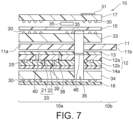
- the security document 1 shown in FIGS. 4 and 5 includes a passport, etc., and contains the information page 10.
- the information page 10 is attached, in a connecting portion 10b, to a cover 2 and other pages 3 of the security document e.g. by sewing.
- the information page 10 includes an information portion 10a, and the connecting portion 10b for attachment to the cover 2 and to the other pages 3.
- the information portion 10a of the information page 10 contains personal information such as the name, the date of birth, a photograph, etc. of a passport holder. Part of the information is printed by using, for example, the below-described laser light technique.
- the connecting portion 10b of the information page 10 is composed of a core layer 11 having a net-like structure.
- the core layer 11 will be described below in greater detail.
- the net-like structure of the connecting portion 10b is formed of a fabric of crossing yarns each composed of a plurality of single fibers.
- the net-like structure may be provided by a method which involves perforating a uniform film to create a desired pattern. What is essential to the present invention is that the net has a sufficient number of "yarns", and that it is quite difficult to attach the yarns to each other without leaving a visible trace associated with attempted counterfeiting.
- the core layer 11 of the connecting portion 10b extends into the information portion 10a.
- the information page 10 of the security document will now be further described with reference to FIGS. 1 through 3 .
- the information page 10 includes the information portion 10a and the connecting portion 10b, and is attached, in the connecting portion 10b, to the cover 2 and the other pages 3 of the security document 1, thus constituting the security document 1.
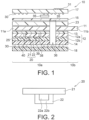
- the information page 10 includes the core layer 11 having flexibility and having a net-like structure, an IC module holding layer 12 provided on the lower surface (one surface) of the core layer 11 via an intermediate layer 13, an IC module 20 held in the IC module holding layer 12, and a laser printing layer 15 provided on the upper surface (the other surface) of the core layer 11 via a first white layer 23.
- the core layer 11 having a net-like structure includes a body portion 11a which is bonded to the IC module holding layer 12, the laser printing layer 15, etc. and which, together with them, constitutes the information portion 10a, and a connecting portion 11b constituting the connecting portion 10b which is composed solely of the core layer 11 and in which the information page 10 is attached to the cover 2 and the other pages 3.
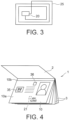
- the IC module 20 includes a substrate 21, and an IC chip 22a provided on the substrate 21 and covered with a sealing resin 22b.
- the IC chip 22a and the sealing resin 22b constitute an IC chip body 22 (see FIG. 2 ).
- the thickness of the IC chip body 22 is larger than the thickness of the substrate 21.
- the thickness of the IC chip body 22 is 50 ⁇ m to 220 ⁇ m, while the thickness of the substrate 21 is 50 ⁇ m to 100 ⁇ m.
- the IC module holding layer 12 includes a substrate accommodating layer 12a accommodating the substrate 21 of the IC module 20 and housing the substrate 21, and an IC chip body accommodating layer (also referred to as an IC chip accommodating layer) 12b accommodating the IC chip body 22 containing the IC chip 22a, and housing the IC chip body 22.
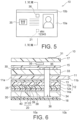
- the antenna 25 is made of copper, and is interposed between the substrate accommodating layer 12a and the IC chip accommodating layer 12b (see FIGS. 1 and 3 ).
- the IC module holding layer 12 has an IC module housing space 40 in which the IC module 20 is housed and which is composed of an opening 38 formed in the substrate accommodating layer 12a, and an opening 39 formed in the IC chip accommodating layer 12b.
- the IC module housing space 40 is closed from above and below with the intermediate layer 13 and with an additional intermediate layer 14 provided on the lower surface of the IC module holding layer 12.
- the laser printing layer 15 is blackened by irradiation with laser light so that a desired character can be displayed.
- the laser printing layer 15 is formed of polycarbonate containing a laser coloring accelerator and, when irradiated with laser light, the laser coloring accelerator has heat energy. The heat energy chars and blackens carbon contained in the polycarbonate in contact with the laser coloring accelerator, resulting in display of a character.
- a first external transparent layer 17 is provided on the upper surface of the laser printing layer 15, and a volume hologram 35 is interposed between the laser printing layer 15 and the first external transparent layer 17.
- the volume hologram 35 can display, for example, a crown in the information page 10 (see FIGS. 4 and 5 ).
- Print 30, such as characters, a pattern, etc., has been formed on the lower surface (inner surface) of the first external transparent layer 17.
- the print 30, such as characters, a pattern, etc. includes information displayed on the front surface of the information page 10 of the security document.
- Such information includes, for example, general information other than individual information such as name and address.
- the individual information such as name and address is formed by irradiating the laser printing layer 15 with laser light.
- a second external transparent layer 18 is provided on the lower surface of the additional intermediate layer 14.
- Print 30, such as characters, a pattern, etc., has been formed also on the upper surface (inner surface) of the second external transparent layer 18.
- the first white layer 23 functions to enhance visibility of the print 30, which has been formed on the lower surface of the first external transparent layer 17, when viewing the print 30 from the side of the first external transparent layer 17.
- the first white layer 23 serves as a background and enables the print 30, which is colored dark and formed on the lower surface of the first external transparent layer 17, to be easily viewed (checked) from the side of the first external transparent layer 17.
- a transparent window 36 made of a transparent material and penetrating the first white layer 23, the core layer 11, the intermediate layer 13, the IC module holding layer 12 and the additional intermediate layer 14.
- the core layer 11 having a net-like structure is made of PET, nylon, or the like.
- the intermediate layer 13, the first external transparent layer 17 and the second external transparent layer 18 are all made of transparent polycarbonate.
- the substrate accommodating layer 12a and the IC chip accommodating layer 12b of the IC module holding layer 12, the first white layer 23 and the additional intermediate layer 14 are all made of white polycarbonate.
- the laser printing layer 15 is made of polycarbonate containing a laser coloring accelerator.
- the intermediate layer 13 and the substrate accommodating layer 12a of the IC module holding layer 12 are laminated together. Subsequently, the substrate 21 of the preformed IC module 20 is inserted into the opening 38 of the substrate accommodating layer 12a. Subsequently, the antenna 25 is disposed on the substrate accommodating layer 12a, and connected to the IC chip 22a of the IC module 20.
- the IC chip accommodating layer 12b is laminated to the substrate accommodating layer 12a.
- the lamination of the IC chip accommodating layer 12b to the substrate accommodating layer 12a is performed such that the IC chip body 22 of the IC module 20 is housed in the opening 39 of the IC chip accommodating layer 12b.
- the additional intermediate layer 14 is laminated to the IC chip accommodating layer 12b.
- the laminate consisting of the intermediate layer 13, the substrate accommodating layer 12a and the IC chip accommodating layer 12b of the IC module holding layer 12, and the additional intermediate layer 14 is subjected to hot pressing to heat and press the laminate, thereby bonding the layers of the laminate together.
- the IC module housing space 40 in which the IC module 20 is housed is surrounded by the intermediate layer 13, the substrate accommodating layer 12a, the IC chip accommodating layer 12b and the additional intermediate layer 14 which are all made of polycarbonate.
- the IC module housing space 40 is surrounded by the polycarbonate materials having approximately the same thermal shrinkage rate. Accordingly, the IC module housing space 40 contracts uniformly with good balance during the hot pressing; therefore, no non-uniform external force will be applied by the interior walls of the IC module housing space 40 to the IC module 20 housed in the IC module housing space 40, resulting in no deformation of the IC module 20. This makes it possible to maintain the performance and the appearance of the IC module 20.
- the core layer 11 and the first white layer 23 are laminated to the laminate consisting of the intermediate layer 13, the IC module holding layer 12 and the additional intermediate layer 14, and then the laser printing layer 15 is laminated to the first white layer 23.
- the volume hologram 35 is provided on the laser printing layer 15, and then the first external transparent layer 17, having the print 30 on the inner surface, is laminated to the laser printing layer 15. Subsequently, the second external transparent layer 18, having the print 30 on the inner surface, is laminated to the additional intermediate layer 14. The resulting laminate is subjected to hot pressing, thereby obtaining the information page 10 of the security document.
- laser light is applied to the laser printing layer 15 of the thus-obtained information page 10 from the side of the first external transparent layer 17 to perform necessary printing on the laser printing layer 15.
- the IC module 20 will not be deformed upon the hot pressing because the intermediate layer 13, the substrate accommodating layer 12a, the IC chip accommodating layer 12b and the additional intermediate layer 14 are all made of polycarbonate. This reduces deformation of the laser printing layer 15 formed over the IC module 20, and can thereby enhance visibility of print formed.
- the volume hologram 35 is interposed between the laser printing layer 15 and the first external transparent layer 17, the volume hologram 35 may be provided at a position corresponding to the transparent window 36 and between the first white layer 23 and the laser printing layer 15 (see the phantom line of FIG. 1 ). By providing the volume hologram 35 at such a position corresponding to the transparent window 36, the volume hologram 35 can be viewed from both the front side and the back side of the information page 10.
- the information page 10 includes an information portion 10a and a connecting portion 10b, and is attached, in the connecting portion 10b, to a cover 2 and other pages 3 of a security document 1, thus constituting the security document 1.
- the information page 10 includes a core layer 11 having flexibility and having a net-like structure, an IC module holding layer 12 provided on the lower surface (one surface) of the core layer 11 via an intermediate layer 13, an IC module 20 held in the IC module holding layer 12, and a laser printing layer 15 provided on the upper surface (the other surface) of the core layer 11 via a first white layer 33.
- the core layer 11 having a net-like structure includes a body portion 11a which is bonded to the IC module holding layer 12, the laser printing layer 15, etc. and which, together with them, constitutes the information portion 10a, and a connecting portion 11b constituting the connecting portion 10b which is composed solely of the core layer 11 and in which the information page 10 is attached to the cover 2 and the other pages 3.
- the IC module 20 is held in the IC module holding layer 12.
- the IC module holding layer 12 includes a substrate accommodating layer 12a accommodating the substrate 21 of the IC module 20 and housing the substrate 21, and an IC chip body accommodating layer (also referred to as an IC chip accommodating layer) 12b accommodating the IC chip body 22 containing the IC chip 22a, and housing the IC chip body 22.
- the antenna 25 is made of copper, and provided on a substrate 25a and, together with the substrate 25a, is interposed between the substrate accommodating layer 12a and the IC chip accommodating layer 12b (see FIG. 6 ).
- the IC module holding layer 12 has an IC module housing space 40 in which the IC module 20 is housed and which is composed of an opening 38 formed in the substrate accommodating layer 12a, and an opening 39 formed in the IC chip accommodating layer 12b.
- the IC module housing space 40 is closed from above and below with the intermediate layer 13 and with an additional intermediate layer 14a provided on the lower surface of the IC module holding layer 12.
- the laser printing layer 15 is blackened by irradiation with laser light so that a desired character can be displayed.
- the laser printing layer 15 is formed of polycarbonate containing a laser coloring accelerator and, when irradiated with laser light, the laser coloring accelerator has heat energy. The heat energy chars and blackens carbon contained in the polycarbonate in contact with the laser coloring accelerator, resulting in display of a character.
- a first external transparent layer 17 is provided on the upper surface of the laser printing layer 15, and a volume hologram 35 is interposed between the laser printing layer 15 and the first external transparent layer 17.
- the volume hologram 35 can display, for example, a crown in the information page 10 (see FIGS. 4 and 5 ).
- Print 30, such as characters, a pattern, etc., has been formed on the upper surface (outer surface) of the first white layer 33.
- a second white layer 34 and a second external transparent layer 18 are provided in this order on the lower surface of the additional intermediate layer 14a.
- Print 30, such as characters, a pattern, etc., has been formed also on the lower surface (outer surface) of the second white layer 34.
- the first white layer 33 functions to enhance visibility of the print 30, which has been formed on the first white layer 33, when viewing the print 30 from the side of the first external transparent layer 17.
- the print 30, which is light-colored, is provided on the first white layer 33, the print 30 can be easily viewed (checked) from the side of the first external transparent layer 17.
- light-colored print 30 has been formed on the second white layer 34. Since the print 30 is provided on the second white layer 34, the print 30 can be easily viewed (checked) from the side of the second external transparent layer 18.
- a transparent window 36 made of a transparent material and penetrating the first white layer 33, the core layer 11, the intermediate layer 13, the IC module holding layer 12, the additional intermediate layer 14a, and the second white layer 34.
- the core layer 11 having a net-like structure is made of PET, nylon, or the like.
- the intermediate layer 13, the first external transparent layer 17, the additional intermediate layer 14a and the second external transparent layer 18 are all made of transparent polycarbonate.
- the substrate accommodating layer 12a and the IC chip accommodating layer 12b of the IC module holding layer 12, the first white layer 33 and the second white layer 34 are all made of white polycarbonate.
- the laser printing layer 15 is made of polycarbonate containing a laser coloring accelerator.
- the overall thickness of the information page 10 shown in FIG. 6 is, for example, 900 ⁇ m.
- the thickness of the first external transparent layer 17 is 105 ⁇ m
- the thickness of the laser printing layer 15 is 50 ⁇ m
- the thickness of the first white layer 33 is 105 ⁇ m
- the thickness of the core layer 11 is 130 ⁇ m
- the thickness of the intermediate layer 13 is 40 ⁇ m
- the thickness of the substrate accommodating layer 12a is 105 ⁇ m
- the thickness of the IC chip accommodating layer 12b is 150 ⁇ m
- the thickness of the additional intermediate layer 14a is 40 ⁇ m
- the thickness of the second white layer 34 is 105 ⁇ m
- the thickness of the second external transparent layer 18 is 50 ⁇ m.
- the intermediate layer 13 and the substrate accommodating layer 12a of the IC module holding layer 12 are laminated together. Subsequently, the substrate 21 of the preformed IC module 20 is inserted into the opening 38 of the substrate accommodating layer 12a.
- the antenna 25 is disposed on the substrate accommodating layer 12a, and connected to the IC chip 22a of the IC module 20.
- the IC chip accommodating layer 12b is laminated to the substrate accommodating layer 12a.
- the lamination of the IC chip accommodating layer 12b to the substrate accommodating layer 12a is performed such that the IC chip body 22 of the IC module 20 is housed in the opening 39 of the IC chip accommodating layer 12b.
- the additional intermediate layer 14a is laminated to the IC chip accommodating layer 12b.
- the laminate consisting of the intermediate layer 13, the substrate accommodating layer 12a and the IC chip accommodating layer 12b of the IC module holding layer 12, and the additional intermediate layer 14a is subjected to hot pressing to heat and press the laminate, thereby bonding the layers of the laminate together.
- the IC module housing space 40 for housing the IC module 20 is surrounded by the intermediate layer 13, the substrate accommodating layer 12a, the IC chip accommodating layer 12b and the additional intermediate layer 14a which are all made of polycarbonate.
- the IC module housing space 40 is surrounded by the polycarbonate materials having approximately the same thermal shrinkage rate. Accordingly, the IC module housing space 40 contracts uniformly with balance during the hot pressing; therefore, no non-uniform external force will be applied by the interior walls of the IC module housing space 40 to the IC module 20 housed in the IC module housing space 40, resulting in no deformation of the IC module 20. This makes it possible to maintain the performance and the appearance of the IC module 20.
- the core layer 11 and the first white layer 33 having the print 30 on the outer surface are laminated to the laminate consisting of the intermediate layer 13, the IC module holding layer 12 and the additional intermediate layer 14a, and then the laser printing layer 15 is laminated to the first white layer 33.
- the volume hologram 35 is provided on the laser printing layer 15, and then the first external transparent layer 17 is laminated to the laser printing layer 15. Subsequently, the second white layer 34, having the print 30 on the outer surface, and the second external transparent layer 18 are laminated sequentially to the additional intermediate layer 14a. The resulting laminate is subjected to hot pressing, thereby obtaining the information page 10 of the security document.
- laser light is applied to the laser printing layer 15 of the thus-obtained information page 10 from the side of the first external transparent layer 17 to perform necessary printing on the laser printing layer 15.
- the IC module 20 will not be deformed upon the hot pressing because the intermediate layer 13, the substrate accommodating layer 12a, the IC chip accommodating layer 12b and the additional intermediate layer 14a are all made of polycarbonate. This reduces deformation of the laser printing layer 15 formed over the IC module 20, and can thereby enhance visibility of print formed.
- the volume hologram 35 is interposed between the laser printing layer 15 and the first external transparent layer 17, the volume hologram 35 may be provided at a position corresponding to the transparent window 36 and between the first white layer 33 and the laser printing layer 15 (see the phantom line of FIG. 6 ). By providing the volume hologram 35 at such a position corresponding to the transparent window 36, the volume hologram 35 can be viewed from both the front side and the back side of the information page 10.
- FIGS. 7 through 8D An information page of a security document according to a third embodiment will now be described with reference to FIGS. 7 through 8D .
- FIGS. 7 through 8D the same symbols are used for the same components or elements as those of the first embodiment shown in FIGS. 1 through 5 or the second embodiment shown in FIG. 6 , and a detailed description thereof is omitted.
- the information page 10 includes an information portion 10a and a connecting portion 10b, and is attached, in the connecting portion 10b, to a cover 2 and other pages 3 of a security document 1, thus constituting the security document 1.
- the information page 10 includes a core layer 11 having flexibility and having a net-like structure, an IC module holding layer 12 provided on the lower surface (one surface) of the core layer 11 via an intermediate layer 13, an IC module 20 held in the IC module holding layer 12, and a laser printing layer 15 provided on the upper surface (the other surface) of the core layer 11 via a first white layer 33.
- the core layer 11 having a net-like structure includes a body portion 11a which is bonded to the IC module holding layer 12, the laser printing layer 15, etc. and which, together with them, constitutes the information portion 10a, and a connecting portion 11b constituting the connecting portion 10b which is composed solely of the core layer 11 and in which the information page 10 is attached to the cover 2 and the other pages 3.
- the IC module 20 is held in the IC module holding layer 12.
- the IC module holding layer 12 includes a substrate accommodating layer 12a accommodating the substrate 21 of the IC module 20 and housing the substrate 21, and an IC chip body accommodating layer (also referred to as an IC chip accommodating layer) 12b accommodating the IC chip body 22 containing the IC chip 22a, and housing the IC chip body 22.
- the antenna 25 is made of copper, and provided on a substrate 25a and, together with the substrate 25a, is interposed between the substrate accommodating layer 12a and the IC chip accommodating layer 12b (see FIG. 7 ).
- the IC module holding layer 12 has an IC module housing space 40 in which the IC module 20 is housed and which is composed of an opening 38 formed in the substrate accommodating layer 12a, and an opening 39 formed in the IC chip accommodating layer 12b.
- the IC module housing space 40 is closed from above and below with the intermediate layer 13 and with an additional intermediate layer 14a provided on the lower surface of the IC module holding layer 12.
- the laser printing layer 15 is blackened by irradiation with laser light so that a desired character can be displayed.
- the laser printing layer 15 is formed of polycarbonate containing a laser coloring accelerator and, when irradiated with laser light, the laser coloring accelerator has heat energy. The heat energy chars and blackens carbon contained in the polycarbonate in contact with the laser coloring accelerator, resulting in display of a character.
- a first external transparent layer 17 is provided on the upper surface of the laser printing layer 15, and a volume hologram 35 is interposed between the laser printing layer 15 and the first external transparent layer 17.
- the volume hologram 35 can display, for example, a crown in the information page 10 (see FIGS. 4 and 5 ).
- Print 30, such as characters, a pattern, etc., has been formed on the lower surface (inner surface) of the first external transparent layer 17 and on the upper surface (outer surface) of the first white layer 33.
- a second white layer 34 and a second external transparent layer 18 are provided in this order on the lower surface of the additional intermediate layer 14a.
- Print 30, such as characters, a pattern, etc., has been formed also on the lower surface (outer surface) of the second white layer 34.
- a transparent window 36 made of a transparent material and penetrating the first white layer 33, the core layer 11, the intermediate layer 13, the IC module holding layer 12, the additional intermediate layer 14a, and the second white layer 34.
- the core layer 11 having a net-like structure is made of PET, nylon, or the like.
- the intermediate layer 13, the first external transparent layer 17, the additional intermediate layer 14a and the second external transparent layer 18 are all made of transparent polycarbonate.
- the substrate accommodating layer 12a and the IC chip accommodating layer 12b of the IC module holding layer 12, the first white layer 33 and the second white layer 34 are all made of white polycarbonate.
- the laser printing layer 15 is made of polycarbonate containing a laser coloring accelerator.
- the first white layer 33 functions to enhance visibility of the print 30, which has been formed on the lower surface of the first external transparent layer 17, when viewing the print 30 from the side of the first external transparent layer 17.
- the first white layer 33 serves as a background and enables the print 30, which is colored dark and formed on the lower surface of the first external transparent layer 17, to be easily viewed (checked) from the side of the first external transparent layer 17.
- Light-colored print 30 has been formed on the first white layer 33. Since the print 30 is provided on the first white layer 33, the print 30 can be easily viewed (checked) from the side of the first external transparent layer 17.
- light-colored print 30 has been formed on the second white layer 34. Since the print 30 is provided on the second white layer 34, the print 30 can be easily viewed (checked) from the side of the second external transparent layer 18.
- the transparent window 36 penetrating the first white layer 33, the core layer 11, the intermediate layer 13, the IC module holding layer 12, the additional intermediate layer 14a, and the second white layer 34, will now be described.
- the transparent window 36 can be set up by sequentially laminating the first white layer 33, the core layer 11, the intermediate layer 13, the IC module holding layer 12 incorporating the IC module 20, the additional intermediate layer 14a, and the second white layer 34, forming a through-hole in the resulting laminate, and then inserting the transparent window 36 of polycarbonate into the through-hole.
- the transparent window 36 of polycarbonate functions to prevent counterfeiting based on the presence/absence of the transparent window 36.
- the transparent window 36 may be formed of half portions 36a, 36a, and an image film 46 having a particular image and interposed between the portions 36a, 36a. In this case, the transparent window 36 having the image film 46 is inserted into the through-hole.
- the information page 10 contains the volume hologram 35 (see FIG. 7 ), including one which displays a crown, provided between the laser printing layer 15 and the first external transparent layer 17.
- the volume hologram 35 can be obtained by transferring a transfer sheet, containing the volume hologram 35, to the upper surface of the laser printing layer 15. Subsequently, the first external transparent layer 17 is laminated to the laser printing layer 15 to which the volume hologram 35 has been transferred.
- volume hologram 35 between the laser printing layer 15 and the first white layer 33 by first transferring a transfer sheet, containing the volume hologram 35, to the lower surface of the laser printing layer 15 to thereby provide the volume hologram 35 on the laser printing layer 15, and then laminating the first white layer 33 to the laser printing layer 15.
- the antenna 25 is connected to the IC module 20 (see FIG. 3 ).
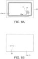
- the antenna 25, connected to the IC module 20, may be disposed as shown in FIGS. 8A through 8D .
- FIG. 8A is a diagram showing the antenna 25 and the IC module 20, disposed on the intermediate layer 13 and the substrate accommodating layer 12a
- FIG. 8B is a diagram showing the antenna 25 and the IC module 20 when viewed from the side of the intermediate layer 13 and the substrate accommodating layer 12a.
- the antenna 25 is disposed in a winding shape on a peripheral portion of the intermediate layer 13 and the substrate accommodating layer 12a, and a part 25a of the antenna 25 extends inward from the winding and is connected to the IC module 20 provided inside the winding of the antenna 25.
- the IC module 20 includes a substrate 21, and an IC chip 22a provided on the substrate 21 and covered with a sealing resin 22b.
- the IC chip 22a and the sealing resin 22b constitute an IC chip body 22.
- the core layer 11 is disposed over the intermediate layer 13 in the above-described embodiments (see FIGS. 1 , 6 and 7 ), the core layer 11 may be disposed under the additional intermediate layer 14 (see FIG. 1 ) or under the additional intermediate layer 14a (see FIGS. 6 and 7 ).
Landscapes
- Engineering & Computer Science (AREA)
- Physics & Mathematics (AREA)
- General Physics & Mathematics (AREA)
- Theoretical Computer Science (AREA)
- Manufacturing & Machinery (AREA)
- Computer Hardware Design (AREA)
- Microelectronics & Electronic Packaging (AREA)
- General Health & Medical Sciences (AREA)
- Electromagnetism (AREA)
- Toxicology (AREA)
- Health & Medical Sciences (AREA)
- Business, Economics & Management (AREA)
- Accounting & Taxation (AREA)
- Finance (AREA)
- Credit Cards Or The Like (AREA)
- Thermal Transfer Or Thermal Recording In General (AREA)
Abstract
Description
- The present invention relates to an information page of a security document having an IC module, such as a passport, and more particularly to an information page of a security document which can prevent deformation of an IC module.
- A security document such as a passport contains an information page with a built-in IC module.
- In general, an information page with a built-in IC module has a multi-layer structure including a plurality of layers, in which the IC module is incorporated.
- Such an information page can be obtained by preparing a multi-layer structure comprised of a laminate of layers, in which an IC module is interposed, and subjecting the multi-layer structure to hot pressing.
- However, it is possible that upon the hot pressing of the multi-layer structure, a non-uniform external force may be applied to the IC module due to differences in thermal shrinkage rate between the layers, resulting in deformation of the IC module.
- Such deformation of the IC module, caused by the application of a non-uniform external force thereto, can affect the performance of the IC module and, in addition, is undesirable in terms of appearance.
- Patent document 1: Published Japanese Translation No.
2009-514708 of the PCT - The present invention has been made in view of the above situation. It is therefore an object of the present invention to provide an information page of a security document in which no non-uniform external force acts on an IC module, and there is no occurrence of deformation of the IC module.
- The present invention provides an information page of a security document, comprising: a core layer having flexibility for incorporating the information page into the security document; an IC module holding layer provided on one surface of the core layer via an intermediate layer; and an IC module held in the IC module holding layer and including a substrate, and an IC chip provided on the substrate, wherein the intermediate layer and the IC module holding layer are both made of polycarbonate.
- In a preferred embodiment of the present invention, the information page further comprises a laser printing layer provided on the other surface of the core layer.
- In a preferred embodiment of the present invention, the IC module holding layer has a multi-layer construction including a substrate accommodating layer accommodating the substrate, and an IC chip accommodating layer accommodating the IC chip, and an antenna, connected to the IC chip of the IC module, is interposed between the substrate accommodating layer and the IC chip accommodating layer.
- In a preferred embodiment of the present invention, a hologram is interposed between any two layers of the information page.
- In a preferred embodiment of the present invention, the information page further comprises a first external transparent layer provided on the laser printing layer and having print formed on its inner surface.
- In a preferred embodiment of the present invention, the information page further comprises a second external transparent layer provided on the IC module holding layer and having print formed on its inner surface.
- In a preferred embodiment of the present invention, the information page further comprises a first white layer provided between the core layer and the laser printing layer and having print formed on its outer surface.
- In a preferred embodiment of the present invention, the information page further comprises a first external transparent layer provided on the laser printing layer.
- In a preferred embodiment of the present invention, the information page further comprises a second white layer provided on the IC module holding layer and having print formed on its outer surface.
- In a preferred embodiment of the present invention, the information page further comprises a transparent window made of a transparent material and penetrating at least the core layer and the IC module holding layer.
- The present invention also provides a security document incorporating any one of the above-described information pages. Advantageous Effects of the Invention
- According to the present invention, no non-uniform external force acts on an IC module upon hot pressing, and therefore there is no occurrence of deformation of the IC module.
-
-
FIG. 1 is a cross-sectional side view of an information page of a security document according to a first embodiment, showing a cross-section in the line-I direction ofFIG. 5 ; -
FIG. 2 is a cross-sectional side view of an IC module; -
FIG. 3 is a diagram showing a positional relationship between an antenna and the IC module; -
FIG. 4 is a perspective view of a security document; -
FIG. 5 is a plan view of the information page; -
FIG. 6 is a cross-sectional side view of an information page of a security document according to a second embodiment, showing a cross-section in the line-VI direction ofFIG. 5 ; -
FIG. 7 is a cross-sectional side view of an information page of a security document according to a third embodiment, showing a cross-section in the line-VII direction ofFIG. 5 ; -
FIG. 8A is a diagram showing an antenna and an IC module, disposed on an intermediate layer and a substrate accommodating layer; -
FIG. 8B is a diagram showing the antenna and the IC module when viewed from the back side of the intermediate layer and the substrate accommodating layer; -
FIG. 8C is an enlarged plan view of the IC module, showing an enlarged view of the portion C ofFIG. 8A ; and -
FIG. 8D is an enlarged cross-sectional view of the IC module. - An information page of a security document according to a first embodiment will now be described in detail with reference to
FIGS. 1 through 5 and some specific examples. - At the outset, the security document incorporating the information page according to the first embodiment will now be described with reference to
FIGS. 4 and5 . - The
security document 1 shown inFIGS. 4 and5 includes a passport, etc., and contains theinformation page 10. Theinformation page 10 is attached, in a connectingportion 10b, to acover 2 andother pages 3 of the security document e.g. by sewing. - The
information page 10 includes aninformation portion 10a, and the connectingportion 10b for attachment to thecover 2 and to theother pages 3. - The
information portion 10a of theinformation page 10 contains personal information such as the name, the date of birth, a photograph, etc. of a passport holder. Part of the information is printed by using, for example, the below-described laser light technique. - As shown in
FIG. 5 , the connectingportion 10b of theinformation page 10 is composed of acore layer 11 having a net-like structure. Thecore layer 11 will be described below in greater detail. The net-like structure of the connectingportion 10b is formed of a fabric of crossing yarns each composed of a plurality of single fibers. - Alternatively, the net-like structure may be provided by a method which involves perforating a uniform film to create a desired pattern. What is essential to the present invention is that the net has a sufficient number of "yarns", and that it is quite difficult to attach the yarns to each other without leaving a visible trace associated with attempted counterfeiting.
- The
core layer 11 of the connectingportion 10b extends into theinformation portion 10a. - The
information page 10 of the security document will now be further described with reference toFIGS. 1 through 3 . As described above, theinformation page 10 includes theinformation portion 10a and the connectingportion 10b, and is attached, in the connectingportion 10b, to thecover 2 and theother pages 3 of thesecurity document 1, thus constituting thesecurity document 1. - The
information page 10 includes thecore layer 11 having flexibility and having a net-like structure, an ICmodule holding layer 12 provided on the lower surface (one surface) of thecore layer 11 via anintermediate layer 13, anIC module 20 held in the ICmodule holding layer 12, and alaser printing layer 15 provided on the upper surface (the other surface) of thecore layer 11 via a firstwhite layer 23. - The
core layer 11 having a net-like structure includes abody portion 11a which is bonded to the ICmodule holding layer 12, thelaser printing layer 15, etc. and which, together with them, constitutes theinformation portion 10a, and a connectingportion 11b constituting the connectingportion 10b which is composed solely of thecore layer 11 and in which theinformation page 10 is attached to thecover 2 and theother pages 3. - The
IC module 20 includes asubstrate 21, and anIC chip 22a provided on thesubstrate 21 and covered with asealing resin 22b. TheIC chip 22a and thesealing resin 22b constitute an IC chip body 22 (seeFIG. 2 ). In the illustrated case, the thickness of theIC chip body 22 is larger than the thickness of thesubstrate 21. For example, the thickness of theIC chip body 22 is 50 µm to 220 µm, while the thickness of thesubstrate 21 is 50 µm to 100 µm. By making the thickness of theIC chip body 22 larger than the thickness of thesubstrate 21, deformation of theentire IC module 20 can be reduced. - The
IC module 20 having the above construction is held in the ICmodule holding layer 12. In the illustrated case, the ICmodule holding layer 12 includes a substrateaccommodating layer 12a accommodating thesubstrate 21 of theIC module 20 and housing thesubstrate 21, and an IC chip body accommodating layer (also referred to as an IC chip accommodating layer) 12b accommodating theIC chip body 22 containing theIC chip 22a, and housing theIC chip body 22. - An
antenna 25, connected to theIC chip 22a of theIC module 20, is disposed between thesubstrate accommodating layer 12a and the IC chipaccommodating layer 12b of the ICmodule holding layer 12. Theantenna 25 is made of copper, and is interposed between thesubstrate accommodating layer 12a and the IC chipaccommodating layer 12b (seeFIGS. 1 and3 ). - The IC
module holding layer 12 has an ICmodule housing space 40 in which theIC module 20 is housed and which is composed of anopening 38 formed in thesubstrate accommodating layer 12a, and anopening 39 formed in the IC chipaccommodating layer 12b. The ICmodule housing space 40 is closed from above and below with theintermediate layer 13 and with an additionalintermediate layer 14 provided on the lower surface of the ICmodule holding layer 12. - The
laser printing layer 15 is blackened by irradiation with laser light so that a desired character can be displayed. To this end, thelaser printing layer 15 is formed of polycarbonate containing a laser coloring accelerator and, when irradiated with laser light, the laser coloring accelerator has heat energy. The heat energy chars and blackens carbon contained in the polycarbonate in contact with the laser coloring accelerator, resulting in display of a character. - A first external
transparent layer 17 is provided on the upper surface of thelaser printing layer 15, and avolume hologram 35 is interposed between thelaser printing layer 15 and the first externaltransparent layer 17. Thevolume hologram 35 can display, for example, a crown in the information page 10 (seeFIGS. 4 and5 ). -
Print 30, such as characters, a pattern, etc., has been formed on the lower surface (inner surface) of the first externaltransparent layer 17. - The
print 30, such as characters, a pattern, etc., includes information displayed on the front surface of theinformation page 10 of the security document. Such information includes, for example, general information other than individual information such as name and address. The individual information such as name and address is formed by irradiating thelaser printing layer 15 with laser light. - A second external
transparent layer 18 is provided on the lower surface of the additionalintermediate layer 14.Print 30, such as characters, a pattern, etc., has been formed also on the upper surface (inner surface) of the second externaltransparent layer 18. - The first
white layer 23 functions to enhance visibility of theprint 30, which has been formed on the lower surface of the first externaltransparent layer 17, when viewing theprint 30 from the side of the first externaltransparent layer 17. - In particular, with the first
white layer 23 provided under the first externaltransparent layer 17, the firstwhite layer 23 serves as a background and enables theprint 30, which is colored dark and formed on the lower surface of the first externaltransparent layer 17, to be easily viewed (checked) from the side of the first externaltransparent layer 17. - There is also provided a
transparent window 36 made of a transparent material and penetrating the firstwhite layer 23, thecore layer 11, theintermediate layer 13, the ICmodule holding layer 12 and the additionalintermediate layer 14. - The materials of the respective layers constituting the
information page 10 will now be described. At the outset, thecore layer 11 having a net-like structure is made of PET, nylon, or the like. - The
intermediate layer 13, the first externaltransparent layer 17 and the second externaltransparent layer 18 are all made of transparent polycarbonate. - The substrate
accommodating layer 12a and the IC chipaccommodating layer 12b of the ICmodule holding layer 12, the firstwhite layer 23 and the additionalintermediate layer 14 are all made of white polycarbonate. - The
laser printing layer 15 is made of polycarbonate containing a laser coloring accelerator. - A method for producing the thus-constructed
information page 10 of the security document will now be described. - First, the
intermediate layer 13 and thesubstrate accommodating layer 12a of the ICmodule holding layer 12 are laminated together. Subsequently, thesubstrate 21 of the preformedIC module 20 is inserted into theopening 38 of thesubstrate accommodating layer 12a. Subsequently, theantenna 25 is disposed on thesubstrate accommodating layer 12a, and connected to theIC chip 22a of theIC module 20. - Thereafter, the IC chip
accommodating layer 12b is laminated to thesubstrate accommodating layer 12a. The lamination of the IC chipaccommodating layer 12b to thesubstrate accommodating layer 12a is performed such that theIC chip body 22 of theIC module 20 is housed in theopening 39 of the IC chipaccommodating layer 12b. Subsequently, the additionalintermediate layer 14 is laminated to the IC chipaccommodating layer 12b. - Thereafter, the laminate consisting of the
intermediate layer 13, thesubstrate accommodating layer 12a and the IC chipaccommodating layer 12b of the ICmodule holding layer 12, and the additionalintermediate layer 14 is subjected to hot pressing to heat and press the laminate, thereby bonding the layers of the laminate together. - The IC
module housing space 40 in which theIC module 20 is housed is surrounded by theintermediate layer 13, thesubstrate accommodating layer 12a, the IC chipaccommodating layer 12b and the additionalintermediate layer 14 which are all made of polycarbonate. Thus, the ICmodule housing space 40 is surrounded by the polycarbonate materials having approximately the same thermal shrinkage rate. Accordingly, the ICmodule housing space 40 contracts uniformly with good balance during the hot pressing; therefore, no non-uniform external force will be applied by the interior walls of the ICmodule housing space 40 to theIC module 20 housed in the ICmodule housing space 40, resulting in no deformation of theIC module 20. This makes it possible to maintain the performance and the appearance of theIC module 20. - Next, the
core layer 11 and the firstwhite layer 23 are laminated to the laminate consisting of theintermediate layer 13, the ICmodule holding layer 12 and the additionalintermediate layer 14, and then thelaser printing layer 15 is laminated to the firstwhite layer 23. - Thereafter, the
volume hologram 35 is provided on thelaser printing layer 15, and then the first externaltransparent layer 17, having theprint 30 on the inner surface, is laminated to thelaser printing layer 15. Subsequently, the second externaltransparent layer 18, having theprint 30 on the inner surface, is laminated to the additionalintermediate layer 14. The resulting laminate is subjected to hot pressing, thereby obtaining theinformation page 10 of the security document. - Next, laser light is applied to the
laser printing layer 15 of the thus-obtainedinformation page 10 from the side of the first externaltransparent layer 17 to perform necessary printing on thelaser printing layer 15. - As described hereinabove, according to this embodiment, no non-uniform external force acts on the
IC module 20 upon the hot pressing, and therefore there is no occurrence of deformation of theIC module 20. In particular, as described above, theIC module 20 will not be deformed upon the hot pressing because theintermediate layer 13, thesubstrate accommodating layer 12a, the IC chipaccommodating layer 12b and the additionalintermediate layer 14 are all made of polycarbonate. This reduces deformation of thelaser printing layer 15 formed over theIC module 20, and can thereby enhance visibility of print formed. - Though in the above-described embodiment the
volume hologram 35 is interposed between thelaser printing layer 15 and the first externaltransparent layer 17, thevolume hologram 35 may be provided at a position corresponding to thetransparent window 36 and between the firstwhite layer 23 and the laser printing layer 15 (see the phantom line ofFIG. 1 ). By providing thevolume hologram 35 at such a position corresponding to thetransparent window 36, thevolume hologram 35 can be viewed from both the front side and the back side of theinformation page 10. - An information page of a security document according to a second embodiment will now be described with reference to
FIG. 6 . - In the second embodiment shown in
FIG. 6 , the same symbols are used for the same components or elements as those of the first embodiment shown inFIGS. 1 through 5 , and a detailed description thereof is omitted. - As shown in
FIG. 6 , theinformation page 10 includes aninformation portion 10a and a connectingportion 10b, and is attached, in the connectingportion 10b, to acover 2 andother pages 3 of asecurity document 1, thus constituting thesecurity document 1. - The
information page 10 includes acore layer 11 having flexibility and having a net-like structure, an ICmodule holding layer 12 provided on the lower surface (one surface) of thecore layer 11 via anintermediate layer 13, anIC module 20 held in the ICmodule holding layer 12, and alaser printing layer 15 provided on the upper surface (the other surface) of thecore layer 11 via a firstwhite layer 33. - The
core layer 11 having a net-like structure includes abody portion 11a which is bonded to the ICmodule holding layer 12, thelaser printing layer 15, etc. and which, together with them, constitutes theinformation portion 10a, and a connectingportion 11b constituting the connectingportion 10b which is composed solely of thecore layer 11 and in which theinformation page 10 is attached to thecover 2 and theother pages 3. - The
IC module 20 is held in the ICmodule holding layer 12. In the illustrated case, the ICmodule holding layer 12 includes a substrateaccommodating layer 12a accommodating thesubstrate 21 of theIC module 20 and housing thesubstrate 21, and an IC chip body accommodating layer (also referred to as an IC chip accommodating layer) 12b accommodating theIC chip body 22 containing theIC chip 22a, and housing theIC chip body 22. - An
antenna 25, connected to theIC chip 22a of theIC module 20, is disposed between thesubstrate accommodating layer 12a and the IC chipaccommodating layer 12b of the ICmodule holding layer 12. Theantenna 25 is made of copper, and provided on asubstrate 25a and, together with thesubstrate 25a, is interposed between thesubstrate accommodating layer 12a and the IC chipaccommodating layer 12b (seeFIG. 6 ). - The IC
module holding layer 12 has an ICmodule housing space 40 in which theIC module 20 is housed and which is composed of anopening 38 formed in thesubstrate accommodating layer 12a, and anopening 39 formed in the IC chipaccommodating layer 12b. The ICmodule housing space 40 is closed from above and below with theintermediate layer 13 and with an additionalintermediate layer 14a provided on the lower surface of the ICmodule holding layer 12. - The
laser printing layer 15 is blackened by irradiation with laser light so that a desired character can be displayed. To this end, thelaser printing layer 15 is formed of polycarbonate containing a laser coloring accelerator and, when irradiated with laser light, the laser coloring accelerator has heat energy. The heat energy chars and blackens carbon contained in the polycarbonate in contact with the laser coloring accelerator, resulting in display of a character. - A first external
transparent layer 17 is provided on the upper surface of thelaser printing layer 15, and avolume hologram 35 is interposed between thelaser printing layer 15 and the first externaltransparent layer 17. Thevolume hologram 35 can display, for example, a crown in the information page 10 (seeFIGS. 4 and5 ). -
Print 30, such as characters, a pattern, etc., has been formed on the upper surface (outer surface) of the firstwhite layer 33. - A second
white layer 34 and a second externaltransparent layer 18 are provided in this order on the lower surface of the additionalintermediate layer 14a.Print 30, such as characters, a pattern, etc., has been formed also on the lower surface (outer surface) of the secondwhite layer 34. - The first
white layer 33 functions to enhance visibility of theprint 30, which has been formed on the firstwhite layer 33, when viewing theprint 30 from the side of the first externaltransparent layer 17. - In particular, since the
print 30, which is light-colored, is provided on the firstwhite layer 33, theprint 30 can be easily viewed (checked) from the side of the first externaltransparent layer 17. - Similarly, light-
colored print 30 has been formed on the secondwhite layer 34. Since theprint 30 is provided on the secondwhite layer 34, theprint 30 can be easily viewed (checked) from the side of the second externaltransparent layer 18. - There is also provided a
transparent window 36 made of a transparent material and penetrating the firstwhite layer 33, thecore layer 11, theintermediate layer 13, the ICmodule holding layer 12, the additionalintermediate layer 14a, and the secondwhite layer 34. - The materials of the respective layers constituting the
information page 10 will now be described. At the outset, thecore layer 11 having a net-like structure is made of PET, nylon, or the like. - The
intermediate layer 13, the first externaltransparent layer 17, the additionalintermediate layer 14a and the second externaltransparent layer 18 are all made of transparent polycarbonate. - The substrate
accommodating layer 12a and the IC chipaccommodating layer 12b of the ICmodule holding layer 12, the firstwhite layer 33 and the secondwhite layer 34 are all made of white polycarbonate. - The
laser printing layer 15 is made of polycarbonate containing a laser coloring accelerator. - The sizes of the respective layers constituting the
information page 10 shown inFIG. 6 will now be described. - The overall thickness of the
information page 10 shown inFIG. 6 is, for example, 900 µm. In one example, the thickness of the first externaltransparent layer 17 is 105 µm, the thickness of thelaser printing layer 15 is 50 µm, the thickness of the firstwhite layer 33 is 105 µm, the thickness of thecore layer 11 is 130 µm, the thickness of theintermediate layer 13 is 40 µm, the thickness of thesubstrate accommodating layer 12a is 105 µm, the thickness of the IC chipaccommodating layer 12b is 150 µm, the thickness of the additionalintermediate layer 14a is 40 µm, the thickness of the secondwhite layer 34 is 105 µm, and the thickness of the second externaltransparent layer 18 is 50 µm. - A method for producing the thus-constructed
information page 10 of the security document will now be described. - First, the
intermediate layer 13 and thesubstrate accommodating layer 12a of the ICmodule holding layer 12 are laminated together. Subsequently, thesubstrate 21 of the preformedIC module 20 is inserted into theopening 38 of thesubstrate accommodating layer 12a. - Subsequently, the
antenna 25 is disposed on thesubstrate accommodating layer 12a, and connected to theIC chip 22a of theIC module 20. - Thereafter, the IC chip
accommodating layer 12b is laminated to thesubstrate accommodating layer 12a. The lamination of the IC chipaccommodating layer 12b to thesubstrate accommodating layer 12a is performed such that theIC chip body 22 of theIC module 20 is housed in theopening 39 of the IC chipaccommodating layer 12b. Subsequently, the additionalintermediate layer 14a is laminated to the IC chipaccommodating layer 12b. - Thereafter, the laminate consisting of the
intermediate layer 13, thesubstrate accommodating layer 12a and the IC chipaccommodating layer 12b of the ICmodule holding layer 12, and the additionalintermediate layer 14a is subjected to hot pressing to heat and press the laminate, thereby bonding the layers of the laminate together. - The IC
module housing space 40 for housing theIC module 20 is surrounded by theintermediate layer 13, thesubstrate accommodating layer 12a, the IC chipaccommodating layer 12b and the additionalintermediate layer 14a which are all made of polycarbonate. Thus, the ICmodule housing space 40 is surrounded by the polycarbonate materials having approximately the same thermal shrinkage rate. Accordingly, the ICmodule housing space 40 contracts uniformly with balance during the hot pressing; therefore, no non-uniform external force will be applied by the interior walls of the ICmodule housing space 40 to theIC module 20 housed in the ICmodule housing space 40, resulting in no deformation of theIC module 20. This makes it possible to maintain the performance and the appearance of theIC module 20. - Next, the
core layer 11 and the firstwhite layer 33 having theprint 30 on the outer surface are laminated to the laminate consisting of theintermediate layer 13, the ICmodule holding layer 12 and the additionalintermediate layer 14a, and then thelaser printing layer 15 is laminated to the firstwhite layer 33. - Thereafter, the
volume hologram 35 is provided on thelaser printing layer 15, and then the first externaltransparent layer 17 is laminated to thelaser printing layer 15. Subsequently, the secondwhite layer 34, having theprint 30 on the outer surface, and the second externaltransparent layer 18 are laminated sequentially to the additionalintermediate layer 14a. The resulting laminate is subjected to hot pressing, thereby obtaining theinformation page 10 of the security document. - Next, laser light is applied to the
laser printing layer 15 of the thus-obtainedinformation page 10 from the side of the first externaltransparent layer 17 to perform necessary printing on thelaser printing layer 15. - As described hereinabove, according to this embodiment, no non-uniform external force acts on the
IC module 20 upon the hot pressing, and therefore there is no occurrence of deformation of theIC module 20. In particular, as described above, theIC module 20 will not be deformed upon the hot pressing because theintermediate layer 13, thesubstrate accommodating layer 12a, the IC chipaccommodating layer 12b and the additionalintermediate layer 14a are all made of polycarbonate. This reduces deformation of thelaser printing layer 15 formed over theIC module 20, and can thereby enhance visibility of print formed. - Though in the above-described embodiment the
volume hologram 35 is interposed between thelaser printing layer 15 and the first externaltransparent layer 17, thevolume hologram 35 may be provided at a position corresponding to thetransparent window 36 and between the firstwhite layer 33 and the laser printing layer 15 (see the phantom line ofFIG. 6 ). By providing thevolume hologram 35 at such a position corresponding to thetransparent window 36, thevolume hologram 35 can be viewed from both the front side and the back side of theinformation page 10. - An information page of a security document according to a third embodiment will now be described with reference to
FIGS. 7 through 8D . - In the third embodiment shown in
FIGS. 7 through 8D , the same symbols are used for the same components or elements as those of the first embodiment shown inFIGS. 1 through 5 or the second embodiment shown inFIG. 6 , and a detailed description thereof is omitted. - As shown in
FIG. 7 , theinformation page 10 includes aninformation portion 10a and a connectingportion 10b, and is attached, in the connectingportion 10b, to acover 2 andother pages 3 of asecurity document 1, thus constituting thesecurity document 1. - The
information page 10 includes acore layer 11 having flexibility and having a net-like structure, an ICmodule holding layer 12 provided on the lower surface (one surface) of thecore layer 11 via anintermediate layer 13, anIC module 20 held in the ICmodule holding layer 12, and alaser printing layer 15 provided on the upper surface (the other surface) of thecore layer 11 via a firstwhite layer 33. - The
core layer 11 having a net-like structure includes abody portion 11a which is bonded to the ICmodule holding layer 12, thelaser printing layer 15, etc. and which, together with them, constitutes theinformation portion 10a, and a connectingportion 11b constituting the connectingportion 10b which is composed solely of thecore layer 11 and in which theinformation page 10 is attached to thecover 2 and theother pages 3. - The
IC module 20 is held in the ICmodule holding layer 12. In this embodiment, the ICmodule holding layer 12 includes a substrateaccommodating layer 12a accommodating thesubstrate 21 of theIC module 20 and housing thesubstrate 21, and an IC chip body accommodating layer (also referred to as an IC chip accommodating layer) 12b accommodating theIC chip body 22 containing theIC chip 22a, and housing theIC chip body 22. - An
antenna 25, connected to theIC chip 22a of theIC module 20, is disposed between thesubstrate accommodating layer 12a and the IC chipaccommodating layer 12b of the ICmodule holding layer 12. Theantenna 25 is made of copper, and provided on asubstrate 25a and, together with thesubstrate 25a, is interposed between thesubstrate accommodating layer 12a and the IC chipaccommodating layer 12b (seeFIG. 7 ). - The IC
module holding layer 12 has an ICmodule housing space 40 in which theIC module 20 is housed and which is composed of anopening 38 formed in thesubstrate accommodating layer 12a, and anopening 39 formed in the IC chipaccommodating layer 12b. The ICmodule housing space 40 is closed from above and below with theintermediate layer 13 and with an additionalintermediate layer 14a provided on the lower surface of the ICmodule holding layer 12. - The
laser printing layer 15 is blackened by irradiation with laser light so that a desired character can be displayed. To this end, thelaser printing layer 15 is formed of polycarbonate containing a laser coloring accelerator and, when irradiated with laser light, the laser coloring accelerator has heat energy. The heat energy chars and blackens carbon contained in the polycarbonate in contact with the laser coloring accelerator, resulting in display of a character. - A first external
transparent layer 17 is provided on the upper surface of thelaser printing layer 15, and avolume hologram 35 is interposed between thelaser printing layer 15 and the first externaltransparent layer 17. Thevolume hologram 35 can display, for example, a crown in the information page 10 (seeFIGS. 4 and5 ). -
Print 30, such as characters, a pattern, etc., has been formed on the lower surface (inner surface) of the first externaltransparent layer 17 and on the upper surface (outer surface) of the firstwhite layer 33. - A second
white layer 34 and a second externaltransparent layer 18 are provided in this order on the lower surface of the additionalintermediate layer 14a.Print 30, such as characters, a pattern, etc., has been formed also on the lower surface (outer surface) of the secondwhite layer 34. - There is also provided a
transparent window 36 made of a transparent material and penetrating the firstwhite layer 33, thecore layer 11, theintermediate layer 13, the ICmodule holding layer 12, the additionalintermediate layer 14a, and the secondwhite layer 34. - The materials of the respective layers constituting the
information page 10 will now be described. At the outset, thecore layer 11 having a net-like structure is made of PET, nylon, or the like. - The
intermediate layer 13, the first externaltransparent layer 17, the additionalintermediate layer 14a and the second externaltransparent layer 18 are all made of transparent polycarbonate. - The substrate
accommodating layer 12a and the IC chipaccommodating layer 12b of the ICmodule holding layer 12, the firstwhite layer 33 and the secondwhite layer 34 are all made of white polycarbonate. - The
laser printing layer 15 is made of polycarbonate containing a laser coloring accelerator. - Of the above layers, the first
white layer 33 functions to enhance visibility of theprint 30, which has been formed on the lower surface of the first externaltransparent layer 17, when viewing theprint 30 from the side of the first externaltransparent layer 17. - In particular, with the first
white layer 33 provided under the first externaltransparent layer 17, the firstwhite layer 33 serves as a background and enables theprint 30, which is colored dark and formed on the lower surface of the first externaltransparent layer 17, to be easily viewed (checked) from the side of the first externaltransparent layer 17. - Light-
colored print 30 has been formed on the firstwhite layer 33. Since theprint 30 is provided on the firstwhite layer 33, theprint 30 can be easily viewed (checked) from the side of the first externaltransparent layer 17. - Further, light-
colored print 30 has been formed on the secondwhite layer 34. Since theprint 30 is provided on the secondwhite layer 34, theprint 30 can be easily viewed (checked) from the side of the second externaltransparent layer 18. - The
transparent window 36, penetrating the firstwhite layer 33, thecore layer 11, theintermediate layer 13, the ICmodule holding layer 12, the additionalintermediate layer 14a, and the secondwhite layer 34, will now be described. - The
transparent window 36 can be set up by sequentially laminating the firstwhite layer 33, thecore layer 11, theintermediate layer 13, the ICmodule holding layer 12 incorporating theIC module 20, the additionalintermediate layer 14a, and the secondwhite layer 34, forming a through-hole in the resulting laminate, and then inserting thetransparent window 36 of polycarbonate into the through-hole. - The
transparent window 36 of polycarbonate functions to prevent counterfeiting based on the presence/absence of thetransparent window 36. Thetransparent window 36 may be formed of half portions 36a, 36a, and animage film 46 having a particular image and interposed between the portions 36a, 36a. In this case, thetransparent window 36 having theimage film 46 is inserted into the through-hole. - The
information page 10 contains the volume hologram 35 (seeFIG. 7 ), including one which displays a crown, provided between thelaser printing layer 15 and the first externaltransparent layer 17. Thevolume hologram 35 can be obtained by transferring a transfer sheet, containing thevolume hologram 35, to the upper surface of thelaser printing layer 15. Subsequently, the first externaltransparent layer 17 is laminated to thelaser printing layer 15 to which thevolume hologram 35 has been transferred. - It is also possible to interpose the
volume hologram 35 between thelaser printing layer 15 and the firstwhite layer 33 by first transferring a transfer sheet, containing thevolume hologram 35, to the lower surface of thelaser printing layer 15 to thereby provide thevolume hologram 35 on thelaser printing layer 15, and then laminating the firstwhite layer 33 to thelaser printing layer 15. - In the above-described embodiments, the
antenna 25 is connected to the IC module 20 (seeFIG. 3 ). Theantenna 25, connected to theIC module 20, may be disposed as shown inFIGS. 8A through 8D . -
FIG. 8A is a diagram showing theantenna 25 and theIC module 20, disposed on theintermediate layer 13 and thesubstrate accommodating layer 12a, andFIG. 8B is a diagram showing theantenna 25 and theIC module 20 when viewed from the side of theintermediate layer 13 and thesubstrate accommodating layer 12a. - As shown in
FIGS. 8A through 8D , theantenna 25 is disposed in a winding shape on a peripheral portion of theintermediate layer 13 and thesubstrate accommodating layer 12a, and apart 25a of theantenna 25 extends inward from the winding and is connected to theIC module 20 provided inside the winding of theantenna 25. - Referring to
FIGS. 8C and 8D , theIC module 20 includes asubstrate 21, and anIC chip 22a provided on thesubstrate 21 and covered with a sealingresin 22b. TheIC chip 22a and the sealingresin 22b constitute anIC chip body 22. - While the
core layer 11 is disposed over theintermediate layer 13 in the above-described embodiments (seeFIGS. 1 ,6 and7 ), thecore layer 11 may be disposed under the additional intermediate layer 14 (seeFIG. 1 ) or under the additionalintermediate layer 14a (seeFIGS. 6 and7 ). - In view of the above, the present application discloses aspects and/or embodiments as described in the following itemized list:
-
Item 1. An information page of a security document, comprising:- a core layer having flexibility for incorporating the information page into the security document;
- an IC module holding layer provided on one surface of the core layer via an intermediate layer; and
- an IC module held in the IC module holding layer and including a substrate, and an IC chip provided on the substrate, wherein the intermediate layer and the IC module holding layer are both made of polycarbonate.
-
Item 2. The information page of a security document according toitem 1, further comprising a laser printing layer provided on the other surface of the core layer. -
Item 3. The information page of a security document according toitem - Item 4. The information page of a security document according to any one of
items 1 to 3, wherein a hologram is interposed between any two layers of the information page. - Item 5. The information page of a security document according to any one of
items 2 to 4, further comprising a first external transparent layer provided on the laser printing layer and having print formed on its inner surface. - Item 6. The information page of a security document according to item 5, further comprising a second external transparent layer provided on the IC module holding layer and having print formed on its inner surface.
-
Item 7. The information page of a security document according to any one ofitems 1 to 4, further comprising a first white layer provided between the core layer and the laser printing layer and having print formed on its outer surface. - Item 8. The information page of a security document according to
item 7, further comprising a first external transparent layer provided on the laser printing layer. - Item 9. The information page of a security document according to
item 7 or 8, further comprising a second white layer provided on the IC module holding layer and having print formed on its outer surface. -
Item 10. The information page of a security document according to any one ofitems 1 to 9, further comprising a transparent window made of a transparent material and penetrating at least the core layer and the IC module holding layer. -
Item 11. A security document incorporating the information page according to any one ofitems 1 to 10. -
- 1 security document
- 10 information page
- 10a information portion
- 10b connecting portion
- 11 core layer
- 11a body portion
- 11b connecting portion
- 12 IC module holding layer
- 12a substrate accommodating layer
- 12b IC chip accommodating layer
- 13 intermediate layer
- 14 additional intermediate layer
- 15 laser printing layer
- 17 first external transparent layer
- 18 second external transparent layer
- 20 IC module
- 21 substrate
- 22 IC chip body
- 22a IC chip
- 22b sealing resin
- 23 first white layer
- 25 antenna
- 30 print
- 31 lenticular lens
- 33 first white layer
- 34 second white layer
- 35 volume hologram
- 36 transparent window
- 40 IC module housing space
Claims (10)
- An information page (10) of a security document (1), comprising:a core layer (11) having flexibility for incorporating the information page into the security document;an IC module holding layer (12) provided on one surface of the core layer (11) via an intermediate layer (13);an additional intermediate layer (14) provided on one surface of the ID module holding layer (12), andan IC module (20) held in the IC module holding layer (12) and including a substrate (21), and an IC chip (22a) provided on the substrate (21), wherein the intermediate layer (13), the IC module holding layer (12) and the additional intermediate layer (14) are made of polycarbonate,further comprising a transparent window (36) made of a transparent material and penetrating at least the core layer (11), the intermediate layer (13), the IC module holding layer (12) and the additional intermediate layer (14).
- The information page (10) of a security document (1) according to claim 1, further comprising a laser printing layer (15) provided on the other surface of the core layer (11).
- The information page (10) of a security document (1) according to claim 1 or 2, wherein the IC module holding layer (12) has a multi-layer construction including a substrate accommodating layer (12a) accommodating the substrate, and an IC chip accommodating layer (12b) accommodating the IC chip (22a), and wherein an antenna (25), connected to the IC chip of the IC module, is interposed between the substrate accommodating layer (12a) and the IC chip accommodating layer (12b).
- The information page (10) of a security document (1) according to any one of claims 1 to 3, wherein the hologram (35) is interposed between any two layers of the information page.
- The information page (10) of a security document (1) according to any one of claims 2 to 4, further comprising a first external transparent layer (17) provided on the laser printing layer (15) and having print formed on its inner surface.
- The information page (10) of a security document (1) according to claim 5, further comprising a second external transparent layer (18) provided on the IC module holding layer (12) and having print formed on its inner surface.
- The information page (10) of a security document (1) according to any one of claims 1 to 4, further comprising a first white layer (23) provided between the core layer (11) and the laser printing layer (17) and having print formed on its outer surface.
- The information page (10) of a security document (1) according to claim 7, further comprising a first external transparent layer (17) provided on the laser printing layer (17).
- The information page (10) of a security document (1) according to claim 7 or 8, further comprising a second white layer (34) provided on the IC module holding layer (12) and having print formed on its outer surface.
- A security document (1) incorporating the information page (10) according to any one of claims 1 to 9.
Applications Claiming Priority (3)
| Application Number | Priority Date | Filing Date | Title |
|---|---|---|---|
| JP2017027038 | 2017-02-16 | ||
| EP18754935.7A EP3584091B1 (en) | 2017-02-16 | 2018-02-15 | Information page |
| PCT/JP2018/005351 WO2018151238A1 (en) | 2017-02-16 | 2018-02-15 | Information page |
Related Parent Applications (2)
| Application Number | Title | Priority Date | Filing Date |
|---|---|---|---|
| EP18754935.7A Division-Into EP3584091B1 (en) | 2017-02-16 | 2018-02-15 | Information page |
| EP18754935.7A Division EP3584091B1 (en) | 2017-02-16 | 2018-02-15 | Information page |
Publications (2)
| Publication Number | Publication Date |
|---|---|
| EP4279290A1 true EP4279290A1 (en) | 2023-11-22 |
| EP4279290B1 EP4279290B1 (en) | 2024-11-20 |
Family
ID=63170671
Family Applications (2)
| Application Number | Title | Priority Date | Filing Date |
|---|---|---|---|
| EP18754935.7A Active EP3584091B1 (en) | 2017-02-16 | 2018-02-15 | Information page |
| EP23200302.0A Active EP4279290B1 (en) | 2017-02-16 | 2018-02-15 | Information page |
Family Applications Before (1)
| Application Number | Title | Priority Date | Filing Date |
|---|---|---|---|
| EP18754935.7A Active EP3584091B1 (en) | 2017-02-16 | 2018-02-15 | Information page |
Country Status (5)
| Country | Link |
|---|---|
| US (2) | US11001092B2 (en) |
| EP (2) | EP3584091B1 (en) |
| JP (2) | JP6970927B2 (en) |
| FI (2) | FI4279290T3 (en) |
| WO (1) | WO2018151238A1 (en) |
Families Citing this family (9)
| Publication number | Priority date | Publication date | Assignee | Title |
|---|---|---|---|---|
| JP6970927B2 (en) * | 2017-02-16 | 2021-11-24 | 大日本印刷株式会社 | Information page |
| JP7147454B2 (en) * | 2018-10-16 | 2022-10-05 | 凸版印刷株式会社 | laminate |
| FI3932685T3 (en) * | 2019-02-28 | 2023-12-05 | Dainippon Printing Co Ltd | Laminate, card base and brochure base made with the same |
| JP7204110B2 (en) * | 2019-05-07 | 2023-01-16 | 独立行政法人 国立印刷局 | Data pages and brochures |
| JP6937998B2 (en) * | 2019-12-19 | 2021-09-22 | 大日本印刷株式会社 | Laminated body, and printing or drawing method for the laminated body |
| JP7375607B2 (en) * | 2020-02-25 | 2023-11-08 | 大日本印刷株式会社 | Information page, security document, IC card, security document inspection system and security document inspection method |
| JP7694581B2 (en) * | 2020-11-13 | 2025-06-18 | 大日本印刷株式会社 | Laminate, booklet, and method of using laminate |
| JP7809269B2 (en) * | 2021-11-25 | 2026-02-02 | 独立行政法人 国立印刷局 | Security page and laminate thermocompression bonding method |
| JP2024005039A (en) * | 2022-06-29 | 2024-01-17 | マクセル株式会社 | IC sheet, passport and contactless IC card equipped with this IC sheet |
Citations (3)
| Publication number | Priority date | Publication date | Assignee | Title |
|---|---|---|---|---|
| WO2004074000A1 (en) * | 2003-02-24 | 2004-09-02 | Sdu Identification B.V. | Identity card and travel document |
| DE102004055495A1 (en) * | 2004-11-17 | 2006-05-24 | Bundesdruckerei Gmbh | Personnel document in booklet form |
| JP2006309603A (en) * | 2005-04-28 | 2006-11-09 | Kyodo Printing Co Ltd | Non-contact IC card |
Family Cites Families (103)
| Publication number | Priority date | Publication date | Assignee | Title |
|---|---|---|---|---|
| DE3689094T2 (en) * | 1985-07-27 | 1994-03-10 | Dainippon Printing Co Ltd | IC card. |
| AUPO799197A0 (en) * | 1997-07-15 | 1997-08-07 | Silverbrook Research Pty Ltd | Image processing method and apparatus (ART01) |
| JP2000168278A (en) | 1998-12-09 | 2000-06-20 | Dainippon Printing Co Ltd | ID card and manufacturing method thereof |
| NL1010841C2 (en) * | 1998-12-18 | 2000-06-20 | Enschede Sdu Bv | Method for manufacturing a booklet, booklet manufactured according to the method and booklet. |
| US20070195392A1 (en) * | 1999-07-08 | 2007-08-23 | Jds Uniphase Corporation | Adhesive Chromagram And Method Of Forming Thereof |
| JP2004021814A (en) * | 2002-06-19 | 2004-01-22 | Konica Minolta Holdings Inc | IC card creation method and IC card |
| JP4062728B2 (en) * | 2002-07-02 | 2008-03-19 | コニカミノルタホールディングス株式会社 | IC card |
| JP4371400B2 (en) * | 2003-02-20 | 2009-11-25 | コニカミノルタエムジー株式会社 | Authentication recording medium creation method |
| JP3100854U (en) | 2003-10-03 | 2004-05-27 | 昌栄印刷株式会社 | Laminated plastic card and IC card |
| US7040981B2 (en) * | 2004-03-11 | 2006-05-09 | Canadian Bank Note Company, Limited | Laminate sheet for security booklets and method for making same |
| US7744002B2 (en) * | 2004-03-11 | 2010-06-29 | L-1 Secure Credentialing, Inc. | Tamper evident adhesive and identification document including same |
| FR2868987B1 (en) * | 2004-04-14 | 2007-02-16 | Arjo Wiggins Secutity Sas Soc | STRUCTURE COMPRISING AN ELECTRONIC DEVICE, IN PARTICULAR FOR THE MANUFACTURE OF A SECURITY OR VALUE DOCUMENT |
| US20080169901A1 (en) * | 2004-07-26 | 2008-07-17 | Koninklijke Philips Electronics N.V. | Arrangement for Identifying Persons |
| FR2877462B1 (en) * | 2004-10-29 | 2007-01-26 | Arjowiggins Security Soc Par A | STRUCTURE COMPRISING AN ELECTRONIC DEVICE FOR THE MANUFACTURE OF A SAFETY DOCUMENT. |
| JP4572659B2 (en) | 2004-10-29 | 2010-11-04 | 凸版印刷株式会社 | Anti-counterfeit card and reading method thereof |
| JP2006163701A (en) | 2004-12-06 | 2006-06-22 | Kokusai Medicom Kk | Personal information recording medium |
| US7745065B2 (en) * | 2005-06-02 | 2010-06-29 | Dai Nippon Printing Co., Ltd. | Volume hologram transfer foil, and volume hologram multilayer structure |
| DE102005028161A1 (en) * | 2005-06-17 | 2006-12-21 | Giesecke & Devrient Gmbh | Thermographically acceptable image-receiving layer for portable data carriers and portable data carriers |
| FI118760B (en) | 2005-11-08 | 2008-03-14 | Setec Oy | Information page and procedure for making an information page |
| NL1031513C2 (en) * | 2006-04-04 | 2007-10-05 | Sdu Identification Bv | Fiber-reinforced binding layer. |
| FR2901899B1 (en) * | 2006-06-06 | 2009-05-08 | Ask Sa | MASKING DEVICE FOR NON-CONTACT PORTABLE OBJECT OF SECURE DOCUMENT TYPE WITH RADIO FREQUENCY DEVICE |
| US8608080B2 (en) * | 2006-09-26 | 2013-12-17 | Feinics Amatech Teoranta | Inlays for security documents |
| US20080179404A1 (en) * | 2006-09-26 | 2008-07-31 | Advanced Microelectronic And Automation Technology Ltd. | Methods and apparatuses to produce inlays with transponders |
| US8322624B2 (en) * | 2007-04-10 | 2012-12-04 | Feinics Amatech Teoranta | Smart card with switchable matching antenna |
| FR2913126B1 (en) * | 2007-02-28 | 2009-07-10 | Arjowiggins Licensing Soc Par | SECURITY DOCUMENT COMPRISING AN RFID DEVICE |
| US7991257B1 (en) * | 2007-05-16 | 2011-08-02 | Fusion Optix, Inc. | Method of manufacturing an optical composite |
| FR2922227B1 (en) * | 2007-10-12 | 2009-12-18 | Arjowiggins Licensing Sas | SHEET COMPRISING AT LEAST ONE OBSERVABLE WATERMARK ON ONE SIDE OF THE SHEET |
| DE102007059746A1 (en) * | 2007-12-07 | 2009-06-10 | Bundesdruckerei Gmbh | Method for producing a security and / or value document with personalized information |
| DE102007052948A1 (en) * | 2007-10-31 | 2009-05-07 | Bayer Materialscience Ag | Process for producing a polycarbonate layer composite |
| DE102007052949A1 (en) * | 2007-10-31 | 2009-05-07 | Bayer Materialscience Ag | Process for producing a polycarbonate layer composite |
| DE102008012419A1 (en) * | 2007-10-31 | 2009-05-07 | Bundesdruckerei Gmbh | Polymer composite layer for security and/or valuable documents comprises at least two interlocking polymer layers joined together with a surface printed with a printed layer absorbing in the visible region in and/or on the composite |
| US20150191037A1 (en) * | 2007-12-07 | 2015-07-09 | Bundesdruckerei Gmbh | Method for producing a security and/or valuable document with personalized information |
| US20130214524A1 (en) * | 2007-12-07 | 2013-08-22 | Bayer Material Science Ag | Method for producing a security and/or valuable document with personalized information |
| JP5487609B2 (en) | 2007-12-28 | 2014-05-07 | 株式会社リコー | Reversible thermosensitive recording medium |
| FR2932908B1 (en) * | 2008-06-24 | 2012-11-16 | Arjowiggins Licensing Sas | STRUCTURE COMPRISING A WATERMARK OR PSEUDO-WATERMARK AND INTEGRATED MICROCIRCUIT DEVICE |
| DE102008035522A1 (en) * | 2008-07-30 | 2010-02-04 | Mühlbauer Ag | Method for producing a device for wireless communication or a prelaminate for such a device |
| US20150227829A1 (en) * | 2008-08-29 | 2015-08-13 | David Finn | Laminates for security documents |
| FR2936075B1 (en) * | 2008-09-12 | 2010-12-31 | Arjowiggins Licensing Sas | STRUCTURE COMPRISING AT LEAST TWO INTEGRATED MICROCIRCUIT DEVICES WITH CONTACTLESS COMMUNICATION |
| DE102008052572A1 (en) * | 2008-10-21 | 2010-04-29 | Bayer Materialscience Ag | Latent-reactive bonded TPU / PC laminates |
| EP2371916A1 (en) * | 2008-12-04 | 2011-10-05 | Nitto Denko Corporation | Double-faced pressure-sensitive adhesive tape for solar cell module |
| WO2010095747A1 (en) * | 2009-02-23 | 2010-08-26 | 日本カラリング株式会社 | Multilayer laser-markable sheet for electronic passport and electronic passport |
| FR2944229B1 (en) * | 2009-04-10 | 2011-05-13 | Arjowiggins Security | STRAIGHT DOCUMENT COMPRISING A STRUCTURE PROVIDED WITH A WATERMARK OR PSEUDO-WATERMARK AND ASSOCIATED METHOD |
| JP4456175B1 (en) * | 2009-10-09 | 2010-04-28 | 日本カラリング株式会社 | Composite hinge sheet for laser marking laminate for electronic passport and laser marking laminate for electronic passport and electronic passport |
| US8613132B2 (en) * | 2009-11-09 | 2013-12-24 | Feinics Amatech Teoranta | Transferring an antenna to an RFID inlay substrate |
| JP2011158788A (en) * | 2010-02-02 | 2011-08-18 | Sony Corp | Hologram-including medium, apparatus for producing hologram-including medium, and information authentication method |
| FR2959581B1 (en) * | 2010-04-28 | 2012-08-17 | Arjowiggins Security | FIBROUS INSERT CONSISTS OF A SINGLE LAYER AND EQUIPPED WITH AN ELECTRONIC DEVICE WITH CONTACTLESS COMMUNICATION. |
| US20120040128A1 (en) * | 2010-08-12 | 2012-02-16 | Feinics Amatech Nominee Limited | Transferring antenna structures to rfid components |
| DK2433810T3 (en) * | 2010-09-24 | 2013-08-12 | Zecca Dello Ist Poligrafico | Electronic passport |
| DE102010046965A1 (en) * | 2010-09-29 | 2012-03-29 | Infineon Technologies Ag | Transponder inlay for a personal identification document and a method of making a transponder inlay |
| JP2012113077A (en) * | 2010-11-24 | 2012-06-14 | Sony Corp | Hologram laminate and manufacturing method of hologram laminate |
| EP2511104A1 (en) * | 2011-04-14 | 2012-10-17 | Gemalto SA | A security document and a manufacturing method thereof |
| PL2540500T3 (en) * | 2011-06-28 | 2017-05-31 | Actilor Intellectual Asset Ag | Lamination device and method for films with temperature-sensitive elements and documents produced with same |
| FR2979852B1 (en) * | 2011-09-14 | 2013-09-27 | Arjowiggins Security | MULTILAYER STRUCTURE INTEGRATING AT LEAST ONE SAFETY ELEMENT |
| DE102011117044B4 (en) * | 2011-10-27 | 2019-05-29 | Bundesdruckerei Gmbh | security element |
| MY151559A (en) * | 2011-11-04 | 2014-06-11 | Iris Corp Berhad | Machine-readable passport with a polycarbonate (pc) datapage and method for making the same |
| FR2982524B1 (en) * | 2011-11-14 | 2013-12-27 | Arjowiggins Security | MULTILAYER STRUCTURE |
| EP2864128A1 (en) * | 2012-06-21 | 2015-04-29 | 3M Innovative Properties Company | A static dissipating laser engravable film |
| US9122966B2 (en) * | 2012-09-07 | 2015-09-01 | Lawrence F. Glaser | Communication device |
| EP2898529B2 (en) * | 2012-09-18 | 2025-02-05 | Assa Abloy Ab | Method of protecting an electrical component in a laminate |
| DE102013000717A1 (en) | 2013-01-17 | 2014-07-17 | Bayer Material Science Ag | Datasheet for a security and / or value document |
| US20140265301A1 (en) * | 2013-03-15 | 2014-09-18 | 3M Innovative Properties Company | Security feature utlizing hinge material and biodata page |
| US10406845B2 (en) * | 2013-03-15 | 2019-09-10 | Gemalto Sa | Flexible hinge material comprising cross-linked polyurethane material |
| DE102013009800B4 (en) * | 2013-06-12 | 2016-07-21 | Bundesdruckerei Gmbh | Method for producing a book-shaped security and / or value document |
| DE102013014309A1 (en) * | 2013-08-29 | 2015-03-05 | Bundesdruckerei Gmbh | Datasheet for a security and / or value document |
| FR3013258B1 (en) * | 2013-11-19 | 2016-02-19 | Hologram Ind | CUSTOMIZABLE DOCUMENT FOR THE MANUFACTURE OF A SAFETY DOCUMENT, PERSONALIZED SECURITY DOCUMENT AND THE PRODUCTION OF SUCH A SECURITY DOCUMENT |
| GB201503135D0 (en) * | 2015-02-25 | 2015-04-08 | Rue De Int Ltd | Booklet |
| US10591756B2 (en) * | 2015-03-31 | 2020-03-17 | Digilens Inc. | Method and apparatus for contact image sensing |
| DE102015005082A1 (en) * | 2015-04-21 | 2016-10-27 | Giesecke & Devrient Gmbh | Multilayer security element |
| US20160355045A1 (en) * | 2015-06-04 | 2016-12-08 | D.A. Offray & Son, Inc. | Security booklet |
| TW201718523A (en) * | 2015-06-23 | 2017-06-01 | 科思創德意志股份有限公司 | New triazine as photo initiators and their preparation |
| GB201512118D0 (en) * | 2015-07-10 | 2015-08-19 | Rue De Int Ltd | Methods of manufacturing security documents and security devices |
| GB2543481B (en) * | 2015-10-05 | 2018-01-31 | De La Rue Int Ltd | A security sheet for an identity document |
| GB2543050A (en) * | 2015-10-05 | 2017-04-12 | De La Rue Int Ltd | A method of manufacturing a security sheet and a security sheet |
| JP6881316B2 (en) * | 2015-12-14 | 2021-06-02 | 大日本印刷株式会社 | Manufacturing method of hinged laminate, hinged laminate array sheet, hinged laminate |
| DE102016203609A1 (en) * | 2016-03-04 | 2017-09-07 | Bundesdruckerei Gmbh | Security article with dynamic and static window security feature and method of manufacture |
| GB201604947D0 (en) * | 2016-03-23 | 2016-05-04 | Rue De Int Ltd | A security document comprising a polymer substrate |
| CA2927176A1 (en) * | 2016-04-15 | 2017-10-15 | Canadian Bank Note Company, Limited | Watermark and other security features for thermoplastic security documents |
| TWI713769B (en) * | 2016-07-21 | 2020-12-21 | 荷蘭商薩比克全球科技公司 | Multilayer identity article and methods of making the same |
| US20190256706A1 (en) * | 2016-10-18 | 2019-08-22 | Mitsubishi Gas Chemical Company, Inc. | Resin composition, resin sheet for card containing resin composition, and multilayer sheet |
| JP6836139B2 (en) * | 2016-12-05 | 2021-02-24 | 大日本印刷株式会社 | Hinged laminates, booklets, laminates |
| DE102017001348A1 (en) * | 2017-02-10 | 2018-08-16 | Giesecke+Devrient Mobile Security Gmbh | Generation of an optical security element |
| JP6970927B2 (en) * | 2017-02-16 | 2021-11-24 | 大日本印刷株式会社 | Information page |
| US12011944B2 (en) * | 2017-03-03 | 2024-06-18 | Dai Nippon Printing Co., Ltd. | Medium issuance system and medium issuance method |
| JP7015293B2 (en) * | 2017-03-06 | 2022-02-02 | 三菱瓦斯化学株式会社 | Resin laminates and cards containing resin laminates |
| DE102017004055B4 (en) * | 2017-04-26 | 2019-05-16 | Mühlbauer Gmbh & Co. Kg | Security deposit with a UV order for a document of identification and method for making a security deposit with a UV order for a document of identification |
| GB2567165B (en) * | 2017-10-04 | 2020-08-26 | De La Rue Int Ltd | Improvements in security sheets comprising security elements |
| PL3473451T5 (en) * | 2017-10-17 | 2024-12-09 | Hid Global Ireland Teoranta | An inlay sheet for a book-like electronic identification document |
| US10479128B2 (en) * | 2017-10-27 | 2019-11-19 | Assa Abloy Ab | Security feature |
| US10821765B2 (en) * | 2018-01-10 | 2020-11-03 | Assa Abloy Ab | Secure documents and methods of manufacturing the same |
| EP3536514A1 (en) * | 2018-03-08 | 2019-09-11 | Thales Dis France SA | Cover sheet, security document and method of manufacturing a security document |
| KR20210099555A (en) * | 2018-12-03 | 2021-08-12 | 코베스트로 인텔렉쳐 프로퍼티 게엠베하 운트 콤파니 카게 | Plastic film with high Vicat softening temperature in layered structure |
| EP3663098A1 (en) * | 2018-12-05 | 2020-06-10 | HID Global CID SAS | Identification document data page and related production method |
| FI3932685T3 (en) * | 2019-02-28 | 2023-12-05 | Dainippon Printing Co Ltd | Laminate, card base and brochure base made with the same |
| BR112021017570A2 (en) * | 2019-03-07 | 2021-11-09 | Covestro Intellectual Property Gmbh & Co Kg | Layered structure for producing a hinge, in particular, for producing multi-layer book covers |
| DE102019002160A1 (en) * | 2019-03-12 | 2020-09-17 | Mühlbauer Gmbh & Co. Kg | Security insert with a tactile lacquer arrangement for an identity document and method for producing such a security insert |
| EP3725536A1 (en) * | 2019-04-18 | 2020-10-21 | Thales Dis France SA | Security document with double verification lenses |
| TWI862590B (en) * | 2019-05-22 | 2024-11-21 | 瑞士商西克帕控股有限公司 | Security document and manufacturing method thereof |
| US11315003B2 (en) * | 2019-08-14 | 2022-04-26 | Federal Card Services, LLC | RFID enabled metal transaction cards |
| EP3835074A1 (en) * | 2019-12-10 | 2021-06-16 | Thales Dis France Sa | Method for securing a security document and security document obtained with this method |
| EP4353487B1 (en) * | 2021-06-09 | 2025-06-25 | Toppan Inc. | 3d display, authenticator, and formation method |
| US12056664B2 (en) * | 2021-08-17 | 2024-08-06 | Monday.com Ltd. | Digital processing systems and methods for external events trigger automatic text-based document alterations in collaborative work systems |
| GB2613016B (en) * | 2021-11-22 | 2024-03-13 | De La Rue Int Ltd | A method of manufacturing a security sheet |
| FR3130195B1 (en) * | 2021-12-13 | 2024-03-01 | Idemia France | Optical device with holographic layer |
-
2018
- 2018-02-15 JP JP2018568617A patent/JP6970927B2/en active Active
- 2018-02-15 EP EP18754935.7A patent/EP3584091B1/en active Active
- 2018-02-15 EP EP23200302.0A patent/EP4279290B1/en active Active
- 2018-02-15 US US16/485,963 patent/US11001092B2/en active Active
- 2018-02-15 FI FIEP23200302.0T patent/FI4279290T3/en active
- 2018-02-15 FI FIEP18754935.7T patent/FI3584091T3/en active
- 2018-02-15 WO PCT/JP2018/005351 patent/WO2018151238A1/en not_active Ceased
-
2021
- 2021-04-12 US US17/227,576 patent/US12403714B2/en active Active
- 2021-10-29 JP JP2021178018A patent/JP7196986B2/en active Active
Patent Citations (3)
| Publication number | Priority date | Publication date | Assignee | Title |
|---|---|---|---|---|
| WO2004074000A1 (en) * | 2003-02-24 | 2004-09-02 | Sdu Identification B.V. | Identity card and travel document |
| DE102004055495A1 (en) * | 2004-11-17 | 2006-05-24 | Bundesdruckerei Gmbh | Personnel document in booklet form |
| JP2006309603A (en) * | 2005-04-28 | 2006-11-09 | Kyodo Printing Co Ltd | Non-contact IC card |
Also Published As
| Publication number | Publication date |
|---|---|
| US20210229482A1 (en) | 2021-07-29 |
| EP3584091B1 (en) | 2024-01-31 |
| US20200062019A1 (en) | 2020-02-27 |
| EP3584091A1 (en) | 2019-12-25 |
| EP3584091A4 (en) | 2020-09-09 |
| WO2018151238A1 (en) | 2018-08-23 |
| JP2022009761A (en) | 2022-01-14 |
| JP6970927B2 (en) | 2021-11-24 |
| FI4279290T3 (en) | 2024-12-20 |
| US12403714B2 (en) | 2025-09-02 |
| EP4279290B1 (en) | 2024-11-20 |
| JPWO2018151238A1 (en) | 2019-12-26 |
| US11001092B2 (en) | 2021-05-11 |
| FI3584091T3 (en) | 2024-03-21 |
| JP7196986B2 (en) | 2022-12-27 |
Similar Documents
| Publication | Publication Date | Title |
|---|---|---|
| US12403714B2 (en) | Information page | |
| AU2004213342B2 (en) | Identity card and travel document | |
| US20140166762A1 (en) | Foil composite card | |
| US10198681B2 (en) | Value or security document comprising an electronic circuit, and method for producing a value or security document | |
| KR102412121B1 (en) | Card, and method for manufacturing card | |
| JP7226471B2 (en) | Hinged Laminate, Hinged Laminate Arrangement Sheet, Hinged Laminate Manufacturing Method | |
| JP2007523415A (en) | Method for manufacturing book type security document and book type security document | |
| CN102197405A (en) | Data storage device and method for production thereof | |
| MX2013003346A (en) | ELECTRONIC PASSPORT. | |
| HK1201960A1 (en) | Machine-readable passport with a polycarbonate (pc) datapage and method for making the same | |
| JP6836139B2 (en) | Hinged laminates, booklets, laminates | |
| JP2020131639A (en) | IC card and its manufacturing method | |
| KR102638812B1 (en) | Laminate, certificate, and method of manufacturing the laminate | |
| US9619744B2 (en) | Colored smart card module | |
| DE19711343A1 (en) | Counterfeit-proof plastic card with optical information | |
| JP2023077437A (en) | Security page and laminate thermocompression method |
Legal Events
| Date | Code | Title | Description |
|---|---|---|---|
| PUAI | Public reference made under article 153(3) epc to a published international application that has entered the european phase |
Free format text: ORIGINAL CODE: 0009012 |
|
| STAA | Information on the status of an ep patent application or granted ep patent |
Free format text: STATUS: THE APPLICATION HAS BEEN PUBLISHED |
|
| AC | Divisional application: reference to earlier application |
Ref document number: 3584091 Country of ref document: EP Kind code of ref document: P |
|
| AK | Designated contracting states |
Kind code of ref document: A1 Designated state(s): AL AT BE BG CH CY CZ DE DK EE ES FI FR GB GR HR HU IE IS IT LI LT LU LV MC MK MT NL NO PL PT RO RS SE SI SK SM TR |
|
| STAA | Information on the status of an ep patent application or granted ep patent |
Free format text: STATUS: REQUEST FOR EXAMINATION WAS MADE |
|
| GRAP | Despatch of communication of intention to grant a patent |
Free format text: ORIGINAL CODE: EPIDOSNIGR1 |
|
| STAA | Information on the status of an ep patent application or granted ep patent |
Free format text: STATUS: GRANT OF PATENT IS INTENDED |
|
| 17P | Request for examination filed |
Effective date: 20240516 |
|
| RBV | Designated contracting states (corrected) |
Designated state(s): AL AT BE BG CH CY CZ DE DK EE ES FI FR GB GR HR HU IE IS IT LI LT LU LV MC MK MT NL NO PL PT RO RS SE SI SK SM TR |
|
| INTG | Intention to grant announced |
Effective date: 20240619 |
|
| GRAS | Grant fee paid |
Free format text: ORIGINAL CODE: EPIDOSNIGR3 |
|
| GRAA | (expected) grant |
Free format text: ORIGINAL CODE: 0009210 |
|
| STAA | Information on the status of an ep patent application or granted ep patent |
Free format text: STATUS: THE PATENT HAS BEEN GRANTED |
|
| P01 | Opt-out of the competence of the unified patent court (upc) registered |
Free format text: CASE NUMBER: APP_54664/2024 Effective date: 20241004 |
|
| AC | Divisional application: reference to earlier application |
Ref document number: 3584091 Country of ref document: EP Kind code of ref document: P |
|
| AK | Designated contracting states |
Kind code of ref document: B1 Designated state(s): AL AT BE BG CH CY CZ DE DK EE ES FI FR GB GR HR HU IE IS IT LI LT LU LV MC MK MT NL NO PL PT RO RS SE SI SK SM TR |
|
| REG | Reference to a national code |
Ref country code: GB Ref legal event code: FG4D |
|
| REG | Reference to a national code |
Ref country code: CH Ref legal event code: EP |
|
| REG | Reference to a national code |
Ref country code: DE Ref legal event code: R096 Ref document number: 602018076892 Country of ref document: DE |
|
| REG | Reference to a national code |
Ref country code: IE Ref legal event code: FG4D |
|
| REG | Reference to a national code |
Ref country code: FI Ref legal event code: FGE |
|
| REG | Reference to a national code |
Ref country code: NL Ref legal event code: FP |
|
| REG | Reference to a national code |
Ref country code: LT Ref legal event code: MG9D |
|
| PG25 | Lapsed in a contracting state [announced via postgrant information from national office to epo] |
Ref country code: IS Free format text: LAPSE BECAUSE OF FAILURE TO SUBMIT A TRANSLATION OF THE DESCRIPTION OR TO PAY THE FEE WITHIN THE PRESCRIBED TIME-LIMIT Effective date: 20250320 Ref country code: PT Free format text: LAPSE BECAUSE OF FAILURE TO SUBMIT A TRANSLATION OF THE DESCRIPTION OR TO PAY THE FEE WITHIN THE PRESCRIBED TIME-LIMIT Effective date: 20250320 Ref country code: HR Free format text: LAPSE BECAUSE OF FAILURE TO SUBMIT A TRANSLATION OF THE DESCRIPTION OR TO PAY THE FEE WITHIN THE PRESCRIBED TIME-LIMIT Effective date: 20241120 |
|
| REG | Reference to a national code |
Ref country code: AT Ref legal event code: MK05 Ref document number: 1743254 Country of ref document: AT Kind code of ref document: T Effective date: 20241120 |
|
| PG25 | Lapsed in a contracting state [announced via postgrant information from national office to epo] |
Ref country code: BG Free format text: LAPSE BECAUSE OF FAILURE TO SUBMIT A TRANSLATION OF THE DESCRIPTION OR TO PAY THE FEE WITHIN THE PRESCRIBED TIME-LIMIT Effective date: 20241120 |
|
| PG25 | Lapsed in a contracting state [announced via postgrant information from national office to epo] |
Ref country code: ES Free format text: LAPSE BECAUSE OF FAILURE TO SUBMIT A TRANSLATION OF THE DESCRIPTION OR TO PAY THE FEE WITHIN THE PRESCRIBED TIME-LIMIT Effective date: 20241120 |
|
| PG25 | Lapsed in a contracting state [announced via postgrant information from national office to epo] |
Ref country code: NO Free format text: LAPSE BECAUSE OF FAILURE TO SUBMIT A TRANSLATION OF THE DESCRIPTION OR TO PAY THE FEE WITHIN THE PRESCRIBED TIME-LIMIT Effective date: 20250220 |
|
| PG25 | Lapsed in a contracting state [announced via postgrant information from national office to epo] |
Ref country code: LV Free format text: LAPSE BECAUSE OF FAILURE TO SUBMIT A TRANSLATION OF THE DESCRIPTION OR TO PAY THE FEE WITHIN THE PRESCRIBED TIME-LIMIT Effective date: 20241120 Ref country code: GR Free format text: LAPSE BECAUSE OF FAILURE TO SUBMIT A TRANSLATION OF THE DESCRIPTION OR TO PAY THE FEE WITHIN THE PRESCRIBED TIME-LIMIT Effective date: 20250221 Ref country code: AT Free format text: LAPSE BECAUSE OF FAILURE TO SUBMIT A TRANSLATION OF THE DESCRIPTION OR TO PAY THE FEE WITHIN THE PRESCRIBED TIME-LIMIT Effective date: 20241120 |
|
| PG25 | Lapsed in a contracting state [announced via postgrant information from national office to epo] |
Ref country code: PL Free format text: LAPSE BECAUSE OF FAILURE TO SUBMIT A TRANSLATION OF THE DESCRIPTION OR TO PAY THE FEE WITHIN THE PRESCRIBED TIME-LIMIT Effective date: 20241120 |
|
| PG25 | Lapsed in a contracting state [announced via postgrant information from national office to epo] |
Ref country code: RS Free format text: LAPSE BECAUSE OF FAILURE TO SUBMIT A TRANSLATION OF THE DESCRIPTION OR TO PAY THE FEE WITHIN THE PRESCRIBED TIME-LIMIT Effective date: 20250220 |
|
| PG25 | Lapsed in a contracting state [announced via postgrant information from national office to epo] |
Ref country code: SM Free format text: LAPSE BECAUSE OF FAILURE TO SUBMIT A TRANSLATION OF THE DESCRIPTION OR TO PAY THE FEE WITHIN THE PRESCRIBED TIME-LIMIT Effective date: 20241120 |
|
| PG25 | Lapsed in a contracting state [announced via postgrant information from national office to epo] |
Ref country code: DK Free format text: LAPSE BECAUSE OF FAILURE TO SUBMIT A TRANSLATION OF THE DESCRIPTION OR TO PAY THE FEE WITHIN THE PRESCRIBED TIME-LIMIT Effective date: 20241120 |
|
| PG25 | Lapsed in a contracting state [announced via postgrant information from national office to epo] |
Ref country code: EE Free format text: LAPSE BECAUSE OF FAILURE TO SUBMIT A TRANSLATION OF THE DESCRIPTION OR TO PAY THE FEE WITHIN THE PRESCRIBED TIME-LIMIT Effective date: 20241120 |
|
| PG25 | Lapsed in a contracting state [announced via postgrant information from national office to epo] |
Ref country code: RO Free format text: LAPSE BECAUSE OF FAILURE TO SUBMIT A TRANSLATION OF THE DESCRIPTION OR TO PAY THE FEE WITHIN THE PRESCRIBED TIME-LIMIT Effective date: 20241120 |
|
| PG25 | Lapsed in a contracting state [announced via postgrant information from national office to epo] |
Ref country code: SK Free format text: LAPSE BECAUSE OF FAILURE TO SUBMIT A TRANSLATION OF THE DESCRIPTION OR TO PAY THE FEE WITHIN THE PRESCRIBED TIME-LIMIT Effective date: 20241120 |
|
| PG25 | Lapsed in a contracting state [announced via postgrant information from national office to epo] |
Ref country code: CZ Free format text: LAPSE BECAUSE OF FAILURE TO SUBMIT A TRANSLATION OF THE DESCRIPTION OR TO PAY THE FEE WITHIN THE PRESCRIBED TIME-LIMIT Effective date: 20241120 |
|
| PG25 | Lapsed in a contracting state [announced via postgrant information from national office to epo] |
Ref country code: IT Free format text: LAPSE BECAUSE OF FAILURE TO SUBMIT A TRANSLATION OF THE DESCRIPTION OR TO PAY THE FEE WITHIN THE PRESCRIBED TIME-LIMIT Effective date: 20241120 |
|
| REG | Reference to a national code |
Ref country code: DE Ref legal event code: R097 Ref document number: 602018076892 Country of ref document: DE |
|
| PG25 | Lapsed in a contracting state [announced via postgrant information from national office to epo] |
Ref country code: SE Free format text: LAPSE BECAUSE OF FAILURE TO SUBMIT A TRANSLATION OF THE DESCRIPTION OR TO PAY THE FEE WITHIN THE PRESCRIBED TIME-LIMIT Effective date: 20241120 |
|
| PG25 | Lapsed in a contracting state [announced via postgrant information from national office to epo] |
Ref country code: MC Free format text: LAPSE BECAUSE OF FAILURE TO SUBMIT A TRANSLATION OF THE DESCRIPTION OR TO PAY THE FEE WITHIN THE PRESCRIBED TIME-LIMIT Effective date: 20241120 |
|
| PLBE | No opposition filed within time limit |
Free format text: ORIGINAL CODE: 0009261 |
|
| STAA | Information on the status of an ep patent application or granted ep patent |
Free format text: STATUS: NO OPPOSITION FILED WITHIN TIME LIMIT |
|
| PG25 | Lapsed in a contracting state [announced via postgrant information from national office to epo] |
Ref country code: LU Free format text: LAPSE BECAUSE OF NON-PAYMENT OF DUE FEES Effective date: 20250215 |
|
| 26N | No opposition filed |
Effective date: 20250821 |
|
| REG | Reference to a national code |
Ref country code: BE Ref legal event code: MM Effective date: 20250228 |
|
| PG25 | Lapsed in a contracting state [announced via postgrant information from national office to epo] |
Ref country code: BE Free format text: LAPSE BECAUSE OF NON-PAYMENT OF DUE FEES Effective date: 20250228 |
|
| REG | Reference to a national code |
Ref country code: CH Ref legal event code: U11 Free format text: ST27 STATUS EVENT CODE: U-0-0-U10-U11 (AS PROVIDED BY THE NATIONAL OFFICE) Effective date: 20260301 |
|
| PGFP | Annual fee paid to national office [announced via postgrant information from national office to epo] |
Ref country code: NL Payment date: 20260218 Year of fee payment: 9 |
|
| PGFP | Annual fee paid to national office [announced via postgrant information from national office to epo] |
Ref country code: GB Payment date: 20260220 Year of fee payment: 9 |
|
| PGFP | Annual fee paid to national office [announced via postgrant information from national office to epo] |
Ref country code: IE Payment date: 20260218 Year of fee payment: 9 Ref country code: DE Payment date: 20260218 Year of fee payment: 9 |
|
| PGFP | Annual fee paid to national office [announced via postgrant information from national office to epo] |
Ref country code: FI Payment date: 20260226 Year of fee payment: 9 |
|
| PGFP | Annual fee paid to national office [announced via postgrant information from national office to epo] |
Ref country code: FR Payment date: 20260219 Year of fee payment: 9 |
|
| PGFP | Annual fee paid to national office [announced via postgrant information from national office to epo] |
Ref country code: CH Payment date: 20260301 Year of fee payment: 9 |
|
| PG25 | Lapsed in a contracting state [announced via postgrant information from national office to epo] |
Ref country code: CY Free format text: LAPSE BECAUSE OF FAILURE TO SUBMIT A TRANSLATION OF THE DESCRIPTION OR TO PAY THE FEE WITHIN THE PRESCRIBED TIME-LIMIT Effective date: 20241120 |
|
| PG25 | Lapsed in a contracting state [announced via postgrant information from national office to epo] |
Ref country code: LT Free format text: LAPSE BECAUSE OF FAILURE TO SUBMIT A TRANSLATION OF THE DESCRIPTION OR TO PAY THE FEE WITHIN THE PRESCRIBED TIME-LIMIT Effective date: 20241120 |
|
| PG25 | Lapsed in a contracting state [announced via postgrant information from national office to epo] |
Ref country code: TR Free format text: LAPSE BECAUSE OF FAILURE TO SUBMIT A TRANSLATION OF THE DESCRIPTION OR TO PAY THE FEE WITHIN THE PRESCRIBED TIME-LIMIT Effective date: 20241120 |