EP4277123A1 - Asymmetrical power amplifier circuit - Google Patents

Asymmetrical power amplifier circuit Download PDF

Info

Publication number
EP4277123A1
EP4277123A1 EP23171932.9A EP23171932A EP4277123A1 EP 4277123 A1 EP4277123 A1 EP 4277123A1 EP 23171932 A EP23171932 A EP 23171932A EP 4277123 A1 EP4277123 A1 EP 4277123A1
Authority
EP
European Patent Office
Prior art keywords
peak
carrier
power
amplifier
output power
Prior art date
Legal status (The legal status is an assumption and is not a legal conclusion. Google has not performed a legal analysis and makes no representation as to the accuracy of the status listed.)
Pending
Application number
EP23171932.9A
Other languages
German (de)
French (fr)
Inventor
Nadim Khlat
Current Assignee (The listed assignees may be inaccurate. Google has not performed a legal analysis and makes no representation or warranty as to the accuracy of the list.)
Qorvo US Inc
Original Assignee
Qorvo US Inc
Priority date (The priority date is an assumption and is not a legal conclusion. Google has not performed a legal analysis and makes no representation as to the accuracy of the date listed.)
Filing date
Publication date
Application filed by Qorvo US Inc filed Critical Qorvo US Inc
Publication of EP4277123A1 publication Critical patent/EP4277123A1/en
Pending legal-status Critical Current

Links

Images

Classifications

    • HELECTRICITY
    • H03ELECTRONIC CIRCUITRY
    • H03FAMPLIFIERS
    • H03F1/00Details of amplifiers with only discharge tubes, only semiconductor devices or only unspecified devices as amplifying elements
    • H03F1/02Modifications of amplifiers to raise the efficiency, e.g. gliding Class A stages, use of an auxiliary oscillation
    • HELECTRICITY
    • H03ELECTRONIC CIRCUITRY
    • H03FAMPLIFIERS
    • H03F1/00Details of amplifiers with only discharge tubes, only semiconductor devices or only unspecified devices as amplifying elements
    • H03F1/02Modifications of amplifiers to raise the efficiency, e.g. gliding Class A stages, use of an auxiliary oscillation
    • H03F1/0205Modifications of amplifiers to raise the efficiency, e.g. gliding Class A stages, use of an auxiliary oscillation in transistor amplifiers
    • H03F1/0288Modifications of amplifiers to raise the efficiency, e.g. gliding Class A stages, use of an auxiliary oscillation in transistor amplifiers using a main and one or several auxiliary peaking amplifiers whereby the load is connected to the main amplifier using an impedance inverter, e.g. Doherty amplifiers
    • HELECTRICITY
    • H03ELECTRONIC CIRCUITRY
    • H03FAMPLIFIERS
    • H03F1/00Details of amplifiers with only discharge tubes, only semiconductor devices or only unspecified devices as amplifying elements
    • H03F1/02Modifications of amplifiers to raise the efficiency, e.g. gliding Class A stages, use of an auxiliary oscillation
    • H03F1/0205Modifications of amplifiers to raise the efficiency, e.g. gliding Class A stages, use of an auxiliary oscillation in transistor amplifiers
    • H03F1/0211Modifications of amplifiers to raise the efficiency, e.g. gliding Class A stages, use of an auxiliary oscillation in transistor amplifiers with control of the supply voltage or current
    • HELECTRICITY
    • H03ELECTRONIC CIRCUITRY
    • H03FAMPLIFIERS
    • H03F1/00Details of amplifiers with only discharge tubes, only semiconductor devices or only unspecified devices as amplifying elements
    • H03F1/56Modifications of input or output impedances, not otherwise provided for
    • H03F1/565Modifications of input or output impedances, not otherwise provided for using inductive elements
    • HELECTRICITY
    • H03ELECTRONIC CIRCUITRY
    • H03FAMPLIFIERS
    • H03F3/00Amplifiers with only discharge tubes or only semiconductor devices as amplifying elements
    • H03F3/189High-frequency amplifiers, e.g. radio frequency amplifiers
    • H03F3/19High-frequency amplifiers, e.g. radio frequency amplifiers with semiconductor devices only
    • H03F3/193High-frequency amplifiers, e.g. radio frequency amplifiers with semiconductor devices only with field-effect devices
    • HELECTRICITY
    • H03ELECTRONIC CIRCUITRY
    • H03FAMPLIFIERS
    • H03F3/00Amplifiers with only discharge tubes or only semiconductor devices as amplifying elements
    • H03F3/20Power amplifiers, e.g. Class B amplifiers, Class C amplifiers
    • H03F3/21Power amplifiers, e.g. Class B amplifiers, Class C amplifiers with semiconductor devices only
    • H03F3/211Power amplifiers, e.g. Class B amplifiers, Class C amplifiers with semiconductor devices only using a combination of several amplifiers
    • HELECTRICITY
    • H03ELECTRONIC CIRCUITRY
    • H03FAMPLIFIERS
    • H03F3/00Amplifiers with only discharge tubes or only semiconductor devices as amplifying elements
    • H03F3/20Power amplifiers, e.g. Class B amplifiers, Class C amplifiers
    • H03F3/24Power amplifiers, e.g. Class B amplifiers, Class C amplifiers of transmitter output stages
    • HELECTRICITY
    • H03ELECTRONIC CIRCUITRY
    • H03FAMPLIFIERS
    • H03F3/00Amplifiers with only discharge tubes or only semiconductor devices as amplifying elements
    • H03F3/20Power amplifiers, e.g. Class B amplifiers, Class C amplifiers
    • H03F3/24Power amplifiers, e.g. Class B amplifiers, Class C amplifiers of transmitter output stages
    • H03F3/245Power amplifiers, e.g. Class B amplifiers, Class C amplifiers of transmitter output stages with semiconductor devices only
    • HELECTRICITY
    • H03ELECTRONIC CIRCUITRY
    • H03FAMPLIFIERS
    • H03F3/00Amplifiers with only discharge tubes or only semiconductor devices as amplifying elements
    • H03F3/45Differential amplifiers
    • H03F3/45071Differential amplifiers with semiconductor devices only
    • H03F3/45076Differential amplifiers with semiconductor devices only characterised by the way of implementation of the active amplifying circuit in the differential amplifier
    • H03F3/45475Differential amplifiers with semiconductor devices only characterised by the way of implementation of the active amplifying circuit in the differential amplifier using IC blocks as the active amplifying circuit
    • HELECTRICITY
    • H03ELECTRONIC CIRCUITRY
    • H03FAMPLIFIERS
    • H03F2200/00Indexing scheme relating to amplifiers
    • H03F2200/273Indexing scheme relating to amplifiers the DC-isolation amplifier, e.g. chopper amplifier, modulation/demodulation amplifier, uses inductive isolation means, e.g. transformers
    • HELECTRICITY
    • H03ELECTRONIC CIRCUITRY
    • H03FAMPLIFIERS
    • H03F2200/00Indexing scheme relating to amplifiers
    • H03F2200/451Indexing scheme relating to amplifiers the amplifier being a radio frequency amplifier
    • HELECTRICITY
    • H03ELECTRONIC CIRCUITRY
    • H03FAMPLIFIERS
    • H03F2200/00Indexing scheme relating to amplifiers
    • H03F2200/541Transformer coupled at the output of an amplifier
    • HELECTRICITY
    • H03ELECTRONIC CIRCUITRY
    • H03FAMPLIFIERS
    • H03F2200/00Indexing scheme relating to amplifiers
    • H03F2200/75Indexing scheme relating to amplifiers the amplifier stage being a common source configuration MOSFET
    • HELECTRICITY
    • H03ELECTRONIC CIRCUITRY
    • H03FAMPLIFIERS
    • H03F2203/00Indexing scheme relating to amplifiers with only discharge tubes or only semiconductor devices as amplifying elements covered by H03F3/00
    • H03F2203/45Indexing scheme relating to differential amplifiers
    • H03F2203/45228A transformer being added at the output or the load circuit of the dif amp

Definitions

  • the technology of the disclosure relates generally to a power amplifier circuit.
  • the fifth generation (5G) system has been widely regarded as the next generation wireless communication system beyond the current third generation (3G) and fourth generation (4G) systems.
  • a 5G-capable wireless communication device is expected to achieve higher data rates, improved coverage range, enhanced signaling efficiency, and reduced latency.
  • the 5G-capable wireless communication device typically includes multiple transmitters to simultaneously transmit multiple 5G radio frequency (RF) signals under such schemes as Carrier Aggregation (CA) and Evolved-Universal Terrestrial Radio Access (E-UTRA) New Radio (NR) Dual Connectivity (DC) (ENDC). Since the transmitters typically transmit the 5G RF signals in a millimeter wave spectrum, the RF signals can be more susceptible to propagation attenuation and interference. To help mitigate propagation attenuation and maintain desirable data throughput, the 5G-capable wireless communication device typically employs multiple power amplifiers to amplify the RF signals to desired power levels before transmitting the RF signals from the transmitters.
  • RF radio frequency
  • Certain arrangements provided herein seek to provide power amplifies that can operate with optimal efficiency, in particular in situations where the RF signals are transmitted with different peak-to-average ratios (PARs).
  • PARs peak-to-average ratios
  • Embodiments of the disclosure relate to an asymmetrical power amplifier circuit.
  • the asymmetrical power amplifier circuit includes a carrier amplifier and a peak amplifier.
  • the carrier amplifier is always active to amplify a radio frequency (RF) to a carrier output power, while the peak amplifier is only active to amplify the RF signal to a peak output power when a time-variant output power of the RF signal is higher than a predefined power threshold.
  • the RF signal in the carrier output power is summed with the RF signal in the peak output power to thereby output the amplified RF signal in the time-variant output power.
  • the carrier output power and the peak output power in the asymmetrical power amplifier are different at the peak of the time-variant output power.
  • the carrier amplifier and the peak amplifier in the asymmetrical power amplifier can both operate with optimal efficiency based on a same modulated voltage.
  • an asymmetrical power amplifier in one aspect, includes a signal input to receive an RF signal in a time-variant input power.
  • the asymmetrical power amplifier also includes a signal output to output the RF signal in a time-variant output power that equals a sum of a carrier output power and a peak output power.
  • the asymmetrical power amplifier also includes a carrier amplifier.
  • the carrier amplifier is configured to amplify the RF signal from the time-variant input power to the carrier output power based on a modulated voltage.
  • the asymmetrical power amplifier also includes a peak amplifier.
  • the peak amplifier is configured to amplify the RF signal from the time-variant input power to the peak output power based on the modulated voltage.
  • the asymmetrical power amplifier also includes an impedance control circuit.
  • the impedance control circuit is coupled to the carrier amplifier and the peak amplifier.
  • the impedance control circuit is configured to cause the carrier output power to be different from the peak output power at the peak of the time-variant output power of the RF signal.
  • a wireless communication circuit in another aspect, includes a transceiver circuit.
  • the transceiver circuit is configured to generate an RF signal in a time-variant input power.
  • the wireless transmission circuit also includes an asymmetrical power amplifier circuit.
  • the asymmetrical power amplifier circuit includes a signal input to receive the RF signal in the time-variant input power.
  • the asymmetrical power amplifier circuit also includes a signal output to output the RF signal in a time-variant output power that equals a sum of a carrier output power and a peak output power.
  • the asymmetrical power amplifier circuit also includes a carrier amplifier.
  • the carrier amplifier is configured to amplify the RF signal from the time-variant input power to the carrier output power based on a modulated voltage.
  • the asymmetrical power amplifier circuit also includes a peak amplifier.
  • the peak amplifier is configured to amplify the RF signal from the time-variant input power to the peak output power based on the modulated voltage.
  • the asymmetrical power amplifier circuit also includes an impedance control circuit.
  • the impedance control circuit is coupled to the carrier amplifier and the peak amplifier.
  • the impedance control circuit is configured to cause the carrier output power to be different from the peak output power at the peak of the time-variant output power of the RF signal.
  • Embodiments of the disclosure relate to an asymmetrical power amplifier circuit.
  • the asymmetrical power amplifier circuit includes a carrier amplifier and a peak amplifier.
  • the carrier amplifier is always active to amplify a radio frequency (RF) to a carrier output power, while the peak amplifier is only active to amplify the RF signal to a peak output power when a time-variant output power of the RF signal is higher than a predefined power threshold.
  • the RF signal in the carrier output power is summed with the RF signal in the peak output power to thereby output the amplified RF signal in the time-variant output power.
  • the carrier output power and the peak output power in the asymmetrical power amplifier are different at the peak of the time-variant output power.
  • the carrier amplifier and the peak amplifier in the asymmetrical power amplifier can both operate with optimal efficiency based on a same modulated voltage.
  • FIG. 1A is a schematic diagram of an example Doherty power amplifier circuit 10, which is commonly known as a symmetrical power amplifier circuit.
  • the Doherty power amplifier circuit 10 is configured to amplify an RF signal 12 from a time-variant input power P IN to a time-variant output power P OUT based on a modulated voltage Vcc.
  • the Doherty power amplifier circuit 10 is coupled to a load circuit 14 (e.g., a transmitter circuit, an antenna circuit, etc.) that can transmit the amplified RF signal 12.
  • a load circuit 14 e.g., a transmitter circuit, an antenna circuit, etc.
  • the Doherty power amplifier circuit 10 includes a carrier amplifier 16C (denoted as "PA-C”) and a peak amplifier 16P (denoted as “PA-P”).
  • the Doherty power amplifier circuit 10 also includes a splitter 18 that splits the RF signal 12 into a carrier signal 20C and a peak signal 20P, each having one-half of the time-variant input power P IN (1 ⁇ 2P IN ).
  • the carrier amplifier 16C is configured to amplify the carrier signal 20C to a carrier output power P OUT-C based on the modulated voltage Vcc.
  • the peak amplifier 16P is configured to amplify the peak signal 20P to a peak output power P OUT-P also based on the modulated voltage Vcc.
  • the modulated voltage Vcc is typically an average power tracking (APT) voltage that keeps track of an average power (e.g., root-mean-square power) of the time-variant output power P OUT .
  • APT average power tracking
  • the carrier amplifier 16C is coupled to a signal output 22 via an impedance inverter 24 and a carrier transfer function (TF) 26C.
  • the impedance inverter 24 and the carrier TF 26C can be configured to collectively modulate a carrier impedance Z M seen by the carrier amplifier 16C.
  • the peak amplifier 16P is coupled to the signal output 22 via a peak TF 26P.
  • the peak TF 26P can be configured to modulate a peak impedance Z P seen by the peak amplifier 16P.
  • the carrier amplifier 16C is always active to amplify the carrier signal 20C to the carrier output power P OUT-C .
  • the peak amplifier 16P is only active when the time-variant output power P OUT is higher than or equal to a predefined power threshold P TH .
  • Figure 1B is a schematic diagram providing an example illustration of an output stage 28 of the carrier amplifier 16C and the peak amplifier 16P in the Doherty power amplifier circuit 10 of Figure 1A .
  • Common elements between Figures 1A and 1B are shown therein with common element numbers and will not be re-described herein.
  • the output stage 28 can include at least one transistor 30, such as a bipolar junction transistor (BJT) or a complementary metal-oxide semiconductor (CMOS) transistor.
  • the transistor 30 can include a base electrode B, a collector electrode C, and an emitter electrode E.
  • the base electrode B is configured to receive a bias voltage V BIAS and the collector electrode C is configured to receive the modulated voltage Vcc.
  • the collector electrode C is also coupled to the signal output 22 that outputs the amplified RF signal 12 at the time-variant output power P OUT .
  • the carrier output power P OUT-C of the amplified carrier signal 12C will be a function of a modulated carrier voltage V OUT-C at the collector electrode C and the carrier impedance Z M , as expressed in equation (Eq. 1) below.
  • P OUT ⁇ C I M * V OUT ⁇ C ⁇ V OUT ⁇ C 2 /Z M
  • I M represents a modulated carrier current generated by the carrier amplifier 16C and Z M represents a modulated carrier impedance seen by the carrier amplifier 16C.
  • the peak output power P OUT-P of the amplified peak signal 12P will be a function of a modulated peak voltage V OUT-P at the collector electrode C and the peak impedance Z P , as expressed in equation (Eq. 2) below.
  • P OUT ⁇ P I P * V OUT ⁇ P ⁇ V OUT ⁇ P 2 /Z P
  • I P represents a modulated peak current generated by the peak amplifier 16P and Z P represents a modulated peak impedance seen by the peak amplifier 16P.
  • the modulated carrier voltage V OUT-C and the modulated peak voltage V OUT-P are both proportionally related to the modulated voltage Vcc, as expressed in equation (Eq. 3) below.
  • V OUT ⁇ C V CC ⁇ V CE
  • V OUT ⁇ P V CC ⁇ V CE
  • V CE represents a collector-emitter voltage, which will be substantially equal to zero when the carrier amplifier 16C and the peak amplifier 16P operate in compression.
  • the modulated carrier voltage V OUT-C and the modulated peak voltage V OUT-P will be substantially equal to the modulated voltage Vcc (V OUT-C ⁇ Vcc, V OUT-P ⁇ Vcc). Accordingly, the carrier amplifier 16C and the peak amplifier 16P will be able to operate with optimal efficiency.
  • the Doherty power amplifier circuit 10 is commonly referred to as a symmetrical power amplifier circuit because of several distinguishable characteristics, as illustrated in Figures 1C-1E .
  • Figures 1C-1E are graphic diagrams providing example illustrations of the distinguishable characteristics of the Doherty power amplifier circuit 10 of Figure 1A .
  • P PEAK time-variant output power
  • Vcc modulated voltage
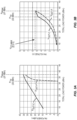
  • Figure 1C shows a relationship between the carrier output power P OUT-C and the peak output power P OUT-P in the Doherty power amplifier circuit 10 of Figure 1A .
  • the predefined power threshold P TH is typically 6 dB below the P PEAK .
  • the P PEAK is assumed to be 37 dBm. Accordingly, the predefined power threshold P TH will be 31 dBm.
  • the carrier amplifier 16C When the time-variant output power P OUT is lower than the predefined power threshold P TH , only the carrier amplifier 16C is active to amplify the carrier signal 20C to the carrier output power P OUT-C .
  • the peak amplifier 16P becomes active to amplify the peak signal 20P to the peak output power P OUT-P , while the carrier amplifier 16C continues to amplify the carrier signal 20C.
  • the carrier output power P OUT-C and the peak output power P OUT-P each equals 34 dBm, which is one-half of the P PEAK . In other words, the carrier output power P OUT-C is equal to the peak output power P OUT-P at the P PEAK .
  • the carrier impedance Z M seen by the carrier amplifier 16C is typically equal to the peak impedance Z P seen by the peak amplifier 16P.
  • the peak amplifier 16P would need to increase the modulated peak current I P at a faster rate than that of the modulated carrier current I M such that the peak output power P OUT-P can become equal to the carrier output power P OUT-C at the P PEAK .
  • Figure 1D shows a relationship between the modulated carrier voltage V OUT-C and the modulated peak voltage V OUT-P in the Doherty power amplifier circuit 10 of Figure 1A .
  • the time-variant output power P OUT is lower than the predefined power threshold P TH , only the carrier amplifier 16C is active.
  • the modulated carrier voltage V OUT-C will increase as the time-variant output power P OUT increases.
  • the peak amplifier 16P becomes active. Accordingly, the modulated peak voltage V OUT-P will increase as the time-variant output power P OUT continues to increase.
  • the carrier amplifier 16C will maintain the modulated carrier voltage V OUT-C constantly at the V CC-MAX .
  • the modulated carrier voltage V OUT-C and the modulated peak voltage V OUT-P are both equal to the V CC-MAX at the P PEAK .
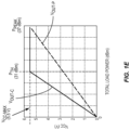
  • Figure 1E shows the modulated voltage Vcc received by the carrier amplifier 16C and the peak amplifier 16D at the respective collector electrode C.
  • the modulated voltage Vcc can be so generated in accordance with the equation (Eq. 3) to be substantially close to the modulated carrier voltage V OUT-C .
  • the carrier amplifier 16C can operate in compression to achieve optimal efficiency.
  • the modulated voltage Vcc reaches, and is maintained at, the V CC-MAX . Thereafter, the peak amplifier 16P becomes active to amplify the peak signal 20P based on the V CC-MAX . Given that the V CC-MAX is always higher than the modulated peak voltage V OUT-P , the peak amplifier 16P will not operate in compression until the time-variant output power P OUT reaches the P PEAK of 37 dBm. In other words, the peak amplifier 16P will not operate with optimal efficiency prior to the P PEAK .
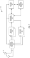
  • FIG 2 is a schematic diagram of an example asymmetrical power amplifier circuit 32 configured according to an embodiment of the present disclosure to achieve improved overall efficiency over the Doherty power amplifier circuit 10 of Figure 1A .
  • the asymmetrical power amplifier circuit 32 includes a carrier amplifier 34C (denoted as "PA-C”), a peak amplifier 34P (denoted as "PA-P”), and a splitter 36.
  • PA-C carrier amplifier
  • PA-P peak amplifier
  • the splitter 36 is configured to split an RF signal 38 into a carrier signal 38C and a peak signal 38P, each having one-half of a time-variant input power P IN of the RF signal 38.
  • the carrier amplifier 34C is always active to amplify the carrier signal 38C to a carrier output power P OUT-C based on a modulated voltage Vcc.
  • the peak amplifier 34P is only active when a time-variant output power P OUT of the RF signal 38 is higher than or equal to a predefined power threshold P TH . When active, the peak amplifier 34P amplifies the peak signal 38P to a peak output power P OUT-P based on the modulated voltage Vcc.
  • each of the carrier amplifier 34C and the peak amplifier 34P can be configured in a similar fashion as illustrated in Figure 1B .
  • the carrier amplifier 34C and the peak amplifier 34P will each operate with optimal efficiency when the modulated voltage Vcc is substantially equal to a modulated carrier voltage V OUT-C and a modulated peak voltage V OUT-P , respectively.
  • the asymmetrical power amplifier circuit 32 differs from the Doherty power amplifier circuit 10 in several aspects.
  • the carrier output power P OUT-C will not be equal to the peak output power P OUT-P at the P PEAK .
  • the carrier output power P OUT-C is higher than the peak output power P OUT-P at the P PEAK .
  • the predefined power threshold P TH in the asymmetrical power amplifier circuit 32 is higher than the predefined power threshold P TH in the Doherty power amplifier circuit 10.
  • the predefined power threshold P TH is set at 31 dBm, which is 6 dB below the P PEAK (37 dBm).
  • the predefined power threshold P TH in the asymmetrical power amplifier circuit 32 can be set at 33 dBm. As a result, the peak amplifier 34P will be activated later than the peak amplifier 16P in the Doherty power amplifier circuit 10.
  • the asymmetrical power amplifier circuit 32 may include a control circuit 40, which can be a field-programmable gate array (FPGA) or an application-specific integrated circuit (ASIC), as an example.
  • the control circuit 40 may be configured to store the predefined power threshold P TH . Accordingly, the control circuit 40 can activate or deactivate the peak amplifier 34P based on the time-variant output power P OUT and the stored predefined power threshold P TH .
  • the control circuit 40 may derive the time-variant output power P OUT from the modulated voltage Vcc and/or the time-variant input power P IN of the RF signal 38 (e.g., via an envelope detector).
  • control circuit 40 may determine the time-variant output power P OUT from an externally generated indication signal 41.
  • the externally generated indication signal 41 can be provided by a transceiver circuit (not shown) that generates the RF signal 38.
  • the asymmetrical power amplifier circuit 32 By configuring the asymmetrical power amplifier circuit 32 to produce the carrier output power P OUT-C and the peak output power P OUT-P at different levels and increasing the predefined power threshold P TH , it is possible to generate the modulated voltage Vcc from a single power management circuit to closely track the modulated carrier voltage V OUT-C , and reduce a gap between the modulated voltage Vcc and the modulated peak voltage V OUT-P . As a result, the carrier amplifier 34C and the peak amplifier 34P may both operate with improved efficiency, thus helping to improve overall efficiency of the asymmetrical power amplifier circuit 32.
  • the asymmetrical power amplifier circuit 32 includes a signal input 42 and a signal output 44.
  • the signal input 42 receives the RF signal 38 in the time-variant input power P IN and the signal output 44 outputs the amplified RF signal 38 in the time-variant output power P OUT .
  • the time-variant output power P OUT will be equal to a sum of the carrier output power P OUT-C and the peak output power P OUT-P when the carrier amplifier 34C and the peak amplifier 34P are both active.
  • the time-variant output power P OUT will be equal to the carrier output power P OUT-C when the peak amplifier 34P is inactive.
  • the asymmetrical power amplifier circuit 32 also includes an impedance inverter circuit 46 and an impedance control circuit 48.
  • the carrier amplifier 34C is coupled to the impedance control circuit 48 via the impedance inverter circuit 46, while the peak amplifier 34P is coupled directly to the impedance control circuit 48.
  • the impedance control circuit 48 is configured to present a modulated carrier impedance Z M and a modulated peak impedance Z P to the carrier amplifier 34C and the peak amplifier 34P, respectively.
  • the modulated peak impedance Z P is higher than the modulated carrier impedance Z M .
  • the peak output power P OUT-P can be lower than the carrier output power P OUT-C according to the equations (Eq. 1 and 2).
  • Figures 3A-3C are graphic diagrams providing example illustrations of some distinctive characteristics of the asymmetrical power amplifier circuit 32 of Figure 2 , as compared to the characteristics of the Doherty power amplifier circuit 10 illustrated in Figures 1C-1E .
  • Figure 3A shows a relationship between the carrier output power P OUT-C and the peak output power P OUT-P in the asymmetrical power amplifier circuit 32 of Figure 2 .
  • the carrier amplifier 34C is active to amplify the carrier signal 38C to the carrier output power P OUT-C .
  • the peak amplifier 34P becomes active to amplify the peak signal 38P to the peak output power P OUT-P , while the carrier amplifier 34C continues to amplify the carrier signal 38C.
  • the carrier output power P OUT-C is higher than the peak output power P OUT-P at the P PEAK .
  • Figure 3B shows a relationship between the modulated carrier voltage V OUT-C and the modulated peak voltage V OUT-P in the asymmetrical power amplifier circuit 32 of Figure 2 .
  • the time-variant output power P OUT is lower than the predefined power threshold P TH , only the carrier amplifier 34C is active.
  • the modulated carrier voltage V OUT-C will increase as the time-variant output power P OUT increases.
  • the peak amplifier 34P becomes active. Accordingly, the modulated peak voltage V OUT-P will increase as the time-variant output power P OUT continues to climb.
  • the carrier amplifier 16C will continue to increase the modulated carrier voltage V OUT-C , as opposed to maintaining the modulated carrier voltage V OUT-C constantly at the V CC-MAX (e.g., 5.5 V).
  • the carrier amplifier 34C can be configured to change the modulated carrier voltage V OUT-C at a first rate (e.g., with a steeper curve) before the peak amplifier 34P becomes active, and at a second rate (e.g., with a flatter curve) slower than the first rate.
  • the modulated carrier voltage V OUT-C and the modulated peak voltage V OUT-P will both increase to the V CC-MAX at the P PEAK .
  • Figure 3C shows the modulated voltage Vcc received by the carrier amplifier 34C and the peak amplifier 34D at a respective collector electrode C.
  • the modulated voltage Vcc can be an envelope tracking (ET) modulated voltage so modulated to closely track the modulated carrier voltage V OUT-C .
  • the carrier amplifier 34C can always operate in compression to achieve optimal efficiency.
  • the modulated voltage Vcc modulated to track the modulated carrier voltage V OUT-C will also be lower than the V CC-MAX prior to the P PEAK .
  • a gap V GAP between the modulated voltage Vcc and the modulated peak voltage V OUT-P will become smaller. Therefore, the efficiency of the peak amplifier 34P may be improved.
  • Figure 4 is a graphic diagram illustrating an efficiency comparison between the asymmetrical power amplifier circuit 32 of Figure 2 and the Doherty power amplifier circuit 10 of Figure 1A .
  • a first efficiency curve 50 of the asymmetrical power amplifier circuit 32 of Figure 2 is compared to a second efficiency curve 52 of the Doherty power amplifier circuit 10 of Figure 1A .
  • the Doherty power amplifier circuit 10 only achieves optimal efficiency at the defined power threshold P TH and the P PEAK .
  • the asymmetrical power amplifier circuit 32 can always achieve a higher efficiency over the Doherty power amplifier circuit 10.
  • the carrier amplifier 34C and the peak amplifier 34P in the asymmetrical power amplifier circuit 32 can each be a differential amplifier.
  • Figure 5 is a schematic diagram of an example asymmetrical power amplifier circuit 54 configured according to an embodiment of the present disclosure. Common elements between Figures 2 and 5 are shown therein with common element numbers and will not be re-described herein.
  • the asymmetrical power amplifier circuit 54 includes a carrier amplifier 56C and a peak amplifier 56P, each configured to operate as a differential amplifier.
  • the impedance control circuit 48 includes a transformer 58 having an input coil 60 and an output coil 62.
  • the modulated voltage Vcc is provided to a center node C of the input coil 60
  • the modulated carrier impedance Z M is provided by a pair of inner nodes A 1 , A 2 of the input coil 60
  • the modulated peak impedance Z P is provided by a pair of outer nodes B 1 , B 2 of the input coil 60.
  • the modulated peak impedance Z P provided by the outer nodes B 1 , B 2 will be higher than the modulated carrier impedance Z M provided by the inner nodes A 1 , A 2 .
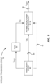
  • Figure 6 is a schematic diagram of an example wireless transmission circuit 64 that can incorporate the asymmetrical power amplifier circuit 32 of Figure 2 and the asymmetrical power amplifier circuit 54 of Figure 5 .
  • Common elements between Figures 2 , 5 , and 6 are shown therein with common element numbers and will not be re-described herein.
  • the wireless transmission circuit 64 includes a transceiver circuit 66 and a power management integrated circuit (PMIC) 68.
  • the transceiver circuit 66 is configured to generate the RF signal 38 in the time-variant input power P IN and provide the RF signal 38 to the asymmetrical power amplifier circuit 32 or the asymmetrical power amplifier circuit 54.
  • the transceiver circuit 66 may also be configured to provide the externally generated indication signal 41 to the control circuit 40.
  • the PMIC 68 is configured to generate the modulated voltage Vcc based on a modulated target voltage V TGT .
  • the transceiver circuit 66 is configured to generate the modulated target voltage V TGT that closely tracks the time-variant input power P IN of the RF signal 38.
  • FIG. 7 is a schematic diagram of an example user element 100 wherein the wireless communication circuit 64 of Figure 6 can be provided.
  • the user element 100 can be any type of user element, such as mobile terminals, smart watches, tablets, computers, navigation devices, access points, and like wireless communication devices that support wireless communications, such as cellular, wireless local area network (WLAN), Bluetooth, and near field communications.
  • the user element 100 will generally include a control system 102, a baseband processor 104, transmit circuitry 106, receive circuitry 108, antenna switching circuitry 110, multiple antennas 112, and user interface circuitry 114.
  • the control system 102 can be a field-programmable gate array (FPGA), as an example.
  • the control system 102 can include at least a microprocessor(s), an embedded memory circuit(s), and a communication bus interface(s).
  • the receive circuitry 108 receives radio frequency signals via the antennas 112 and through the antenna switching circuitry 110 from one or more base stations.
  • a low noise amplifier and a filter cooperate to amplify and remove broadband interference from the received signal for processing.
  • Downconversion and digitization circuitry (not shown) will then downconvert the filtered, received signal to an intermediate or baseband frequency signal, which is then digitized into one or more digital streams using analog-to-digital converter(s) (ADC).
  • ADC analog-to-digital converter
  • the baseband processor 104 processes the digitized received signal to extract the information or data bits conveyed in the received signal. This processing typically comprises demodulation, decoding, and error correction operations, as will be discussed in greater detail below.
  • the baseband processor 104 is generally implemented in one or more digital signal processors (DSPs) and application specific integrated circuits (ASICs).
  • DSPs digital signal processors
  • ASICs application specific integrated circuits
  • the baseband processor 104 receives digitized data, which may represent voice, data, or control information, from the control system 102, which it encodes for transmission.
  • the encoded data is output to the transmit circuitry 106, where a digital-to-analog converter(s) (DAC) converts the digitally encoded data into an analog signal and a modulator modulates the analog signal onto a carrier signal that is at a desired transmit frequency or frequencies.
  • DAC digital-to-analog converter
  • a power amplifier will amplify the modulated carrier signal to a level appropriate for transmission, and deliver the modulated carrier signal to the antennas 112 through the antenna switching circuitry 110.
  • the multiple antennas 112 and the replicated transmit and receive circuitries 106, 108 may provide spatial diversity. Modulation and processing details will be understood by those skilled in the art.
  • the asymmetrical power amplifier circuit includes a carrier amplifier and a peak amplifier.
  • the carrier amplifier is always active to amplify a radio frequency (RF) to a carrier output power, while the peak amplifier is only active to amplify the RF signal to a peak output power when a time-variant output power of the RF signal is higher than a predefined power threshold.
  • the RF signal in the carrier output power is summed with the RF signal in the peak output power to thereby output the amplified RF signal in the time-variant output power.
  • the carrier output power and the peak output power are different at a peak of the time-variant output power. As such, the carrier amplifier and the peak amplifier can both operate with optimal efficiency based on a same modulated voltage.

Landscapes

  • Engineering & Computer Science (AREA)
  • Power Engineering (AREA)
  • Amplifiers (AREA)

Abstract

An asymmetrical power amplifier circuit is provided. The asymmetrical power amplifier circuit includes a carrier amplifier and a peak amplifier. The carrier amplifier is always active to amplify a radio frequency (RF) to a carrier output power, while the peak amplifier is only active to amplify the RF signal to a peak output power when a time-variant output power of the RF signal is higher than a predefined power threshold. The RF signal in the carrier output power is summed with the RF signal in the peak output power to thereby output the amplified RF signal in the time-variant output power. Unlike a conventional symmetrical power amplifier, the carrier output power and the peak output power are different at a peak of the time-variant output power. As such, the carrier amplifier and the peak amplifier can both operate with optimal efficiency based on a same modulated voltage.

Description

    Related Applications
  • This application claims the benefit of U.S. provisional patent application serial number 63/341,127, filed on May 12, 2022 , the disclosure of which is hereby incorporated herein by reference in its entirety.
  • Field of the Disclosure
  • The technology of the disclosure relates generally to a power amplifier circuit.
  • Background
  • The fifth generation (5G) system has been widely regarded as the next generation wireless communication system beyond the current third generation (3G) and fourth generation (4G) systems. In this regard, a 5G-capable wireless communication device is expected to achieve higher data rates, improved coverage range, enhanced signaling efficiency, and reduced latency.
  • The 5G-capable wireless communication device typically includes multiple transmitters to simultaneously transmit multiple 5G radio frequency (RF) signals under such schemes as Carrier Aggregation (CA) and Evolved-Universal Terrestrial Radio Access (E-UTRA) New Radio (NR) Dual Connectivity (DC) (ENDC). Since the transmitters typically transmit the 5G RF signals in a millimeter wave spectrum, the RF signals can be more susceptible to propagation attenuation and interference. To help mitigate propagation attenuation and maintain desirable data throughput, the 5G-capable wireless communication device typically employs multiple power amplifiers to amplify the RF signals to desired power levels before transmitting the RF signals from the transmitters.
  • Summary
  • Particular aspects are set out in the appended independent claims. Various optional embodiments are set out in the dependent claims.
  • Certain arrangements provided herein seek to provide power amplifies that can operate with optimal efficiency, in particular in situations where the RF signals are transmitted with different peak-to-average ratios (PARs).
  • Embodiments of the disclosure relate to an asymmetrical power amplifier circuit. The asymmetrical power amplifier circuit includes a carrier amplifier and a peak amplifier. The carrier amplifier is always active to amplify a radio frequency (RF) to a carrier output power, while the peak amplifier is only active to amplify the RF signal to a peak output power when a time-variant output power of the RF signal is higher than a predefined power threshold. The RF signal in the carrier output power is summed with the RF signal in the peak output power to thereby output the amplified RF signal in the time-variant output power. Unlike a conventional symmetrical power amplifier, wherein the carrier output power is equal to the peak output power at a peak of the time-variant output power, the carrier output power and the peak output power in the asymmetrical power amplifier are different at the peak of the time-variant output power. As a result, the carrier amplifier and the peak amplifier in the asymmetrical power amplifier can both operate with optimal efficiency based on a same modulated voltage.
  • In one aspect, an asymmetrical power amplifier is provided. The asymmetrical power amplifier includes a signal input to receive an RF signal in a time-variant input power. The asymmetrical power amplifier also includes a signal output to output the RF signal in a time-variant output power that equals a sum of a carrier output power and a peak output power. The asymmetrical power amplifier also includes a carrier amplifier. The carrier amplifier is configured to amplify the RF signal from the time-variant input power to the carrier output power based on a modulated voltage. The asymmetrical power amplifier also includes a peak amplifier. The peak amplifier is configured to amplify the RF signal from the time-variant input power to the peak output power based on the modulated voltage. The asymmetrical power amplifier also includes an impedance control circuit. The impedance control circuit is coupled to the carrier amplifier and the peak amplifier. The impedance control circuit is configured to cause the carrier output power to be different from the peak output power at the peak of the time-variant output power of the RF signal.
  • In another aspect, a wireless communication circuit is provided. The wireless communication circuit includes a transceiver circuit. The transceiver circuit is configured to generate an RF signal in a time-variant input power. The wireless transmission circuit also includes an asymmetrical power amplifier circuit. The asymmetrical power amplifier circuit includes a signal input to receive the RF signal in the time-variant input power. The asymmetrical power amplifier circuit also includes a signal output to output the RF signal in a time-variant output power that equals a sum of a carrier output power and a peak output power. The asymmetrical power amplifier circuit also includes a carrier amplifier. The carrier amplifier is configured to amplify the RF signal from the time-variant input power to the carrier output power based on a modulated voltage. The asymmetrical power amplifier circuit also includes a peak amplifier. The peak amplifier is configured to amplify the RF signal from the time-variant input power to the peak output power based on the modulated voltage. The asymmetrical power amplifier circuit also includes an impedance control circuit. The impedance control circuit is coupled to the carrier amplifier and the peak amplifier. The impedance control circuit is configured to cause the carrier output power to be different from the peak output power at the peak of the time-variant output power of the RF signal.
  • Those skilled in the art will appreciate the scope of the present disclosure and realize additional aspects thereof after reading the following detailed description of the illustrative embodiments in association with the accompanying drawing figures.
  • Brief Description of the Drawing Figures
  • The accompanying drawing figures incorporated in and forming a part of this specification illustrate several aspects of the disclosure, and together with the description serve to explain the principles of the disclosure.
    • Figure 1A is a schematic diagram of an example Doherty power amplifier circuit, which is commonly known as a symmetrical power amplifier circuit;
    • Figure 1B is a schematic diagram providing an example illustration of an output stage of a carrier amplifier and a peak amplifier in the Doherty power amplifier circuit of Figure 1A;
    • Figures 1C-1E are graphic diagrams providing example illustrations of characteristics of the Doherty power amplifier circuit of Figure 1A;
    • Figure 2 is a schematic diagram of an example asymmetrical power amplifier circuit configured according to an embodiment of the present disclosure to achieve improved overall efficiency over the Doherty power amplifier circuit of Figure 1A;
    • Figures 3A-3C are graphic diagrams providing example illustrations of some distinctive characteristics of the asymmetrical power amplifier circuit of Figure 2, as compared to the characteristics of the Doherty power amplifier circuit illustrated in Figures 1C-1E;
    • Figure 4 is a graphic diagram illustrating an efficiency comparison between the asymmetrical power amplifier circuit of Figure 2 and the Doherty power amplifier circuit of Figure 1A;
    • Figure 5 is a schematic diagram of an example asymmetrical power amplifier circuit configured according to an embodiment of the present disclosure;
    • Figure 6 is a schematic diagram of an example wireless communication circuit that can be configured to incorporate the asymmetrical power amplifier circuits of Figures 2 and 5; and
    • Figure 7 is a schematic diagram of an example user element wherein the wireless communication circuit of Figure 6 can be provided.
    Detailed Description
  • The embodiments set forth below represent the necessary information to enable those skilled in the art to practice the embodiments and illustrate the best mode of practicing the embodiments. Upon reading the following description in light of the accompanying drawing figures, those skilled in the art will understand the concepts of the disclosure and will recognize applications of these concepts not particularly addressed herein. It should be understood that these concepts and applications fall within the scope of the disclosure and the accompanying claims.
  • It will be understood that, although the terms first, second, etc. may be used herein to describe various elements, these elements should not be limited by these terms. These terms are only used to distinguish one element from another. For example, a first element could be termed a second element, and, similarly, a second element could be termed a first element, without departing from the scope of the present disclosure. As used herein, the term "and/or" includes any and all combinations of one or more of the associated listed items.
  • It will be understood that when an element such as a layer, region, or substrate is referred to as being "on" or extending "onto" another element, it can be directly on or extend directly onto the other element or intervening elements may also be present. In contrast, when an element is referred to as being "directly on" or extending "directly onto" another element, there are no intervening elements present. Likewise, it will be understood that when an element such as a layer, region, or substrate is referred to as being "over" or extending "over" another element, it can be directly over or extend directly over the other element or intervening elements may also be present. In contrast, when an element is referred to as being "directly over" or extending "directly over" another element, there are no intervening elements present. It will also be understood that when an element is referred to as being "connected" or "coupled" to another element, it can be directly connected or coupled to the other element or intervening elements may be present. In contrast, when an element is referred to as being "directly connected" or "directly coupled" to another element, there are no intervening elements present.
  • Relative terms such as "below" or "above" or "upper" or "lower" or "horizontal" or "vertical" may be used herein to describe a relationship of one element, layer, or region to another element, layer, or region as illustrated in the Figures. It will be understood that these terms and those discussed above are intended to encompass different orientations of the device in addition to the orientation depicted in the Figures.
  • The terminology used herein is for the purpose of describing particular embodiments only and is not intended to be limiting of the disclosure. As used herein, the singular forms "a," "an," and "the" are intended to include the plural forms as well, unless the context clearly indicates otherwise. It will be further understood that the terms "comprises," "comprising," "includes," and/or "including" when used herein specify the presence of stated features, integers, steps, operations, elements, and/or components, but do not preclude the presence or addition of one or more other features, integers, steps, operations, elements, components, and/or groups thereof.
  • Unless otherwise defined, all terms (including technical and scientific terms) used herein have the same meaning as commonly understood by one of ordinary skill in the art to which this disclosure belongs. It will be further understood that terms used herein should be interpreted as having a meaning that is consistent with their meaning in the context of this specification and the relevant art and will not be interpreted in an idealized or overly formal sense unless expressly so defined herein.
  • Embodiments of the disclosure relate to an asymmetrical power amplifier circuit. The asymmetrical power amplifier circuit includes a carrier amplifier and a peak amplifier. The carrier amplifier is always active to amplify a radio frequency (RF) to a carrier output power, while the peak amplifier is only active to amplify the RF signal to a peak output power when a time-variant output power of the RF signal is higher than a predefined power threshold. The RF signal in the carrier output power is summed with the RF signal in the peak output power to thereby output the amplified RF signal in the time-variant output power. Unlike a conventional symmetrical power amplifier, wherein the carrier output power is equal to the peak output power at a peak of the time-variant output power, the carrier output power and the peak output power in the asymmetrical power amplifier are different at the peak of the time-variant output power. As a result, the carrier amplifier and the peak amplifier in the asymmetrical power amplifier can both operate with optimal efficiency based on a same modulated voltage.
  • Before discussing the asymmetrical power amplifier circuit according to the present disclosure, starting at Figure 2, an overview of a standard Doherty power amplifier circuit is first provided with reference to Figures 1A-1F to help understand the configuration and operation of a conventional symmetrical power amplifier circuit.
  • Figure 1A is a schematic diagram of an example Doherty power amplifier circuit 10, which is commonly known as a symmetrical power amplifier circuit. The Doherty power amplifier circuit 10 is configured to amplify an RF signal 12 from a time-variant input power PIN to a time-variant output power POUT based on a modulated voltage Vcc. The Doherty power amplifier circuit 10 is coupled to a load circuit 14 (e.g., a transmitter circuit, an antenna circuit, etc.) that can transmit the amplified RF signal 12.
  • The Doherty power amplifier circuit 10 includes a carrier amplifier 16C (denoted as "PA-C") and a peak amplifier 16P (denoted as "PA-P"). The Doherty power amplifier circuit 10 also includes a splitter 18 that splits the RF signal 12 into a carrier signal 20C and a peak signal 20P, each having one-half of the time-variant input power PIN (½PIN). The carrier amplifier 16C is configured to amplify the carrier signal 20C to a carrier output power POUT-C based on the modulated voltage Vcc. Likewise, the peak amplifier 16P is configured to amplify the peak signal 20P to a peak output power POUT-P also based on the modulated voltage Vcc. The modulated voltage Vcc is typically an average power tracking (APT) voltage that keeps track of an average power (e.g., root-mean-square power) of the time-variant output power POUT.
  • The carrier amplifier 16C is coupled to a signal output 22 via an impedance inverter 24 and a carrier transfer function (TF) 26C. The impedance inverter 24 and the carrier TF 26C can be configured to collectively modulate a carrier impedance ZM seen by the carrier amplifier 16C. The peak amplifier 16P is coupled to the signal output 22 via a peak TF 26P. The peak TF 26P can be configured to modulate a peak impedance ZP seen by the peak amplifier 16P.
  • In the Doherty power amplifier circuit 10, the carrier amplifier 16C is always active to amplify the carrier signal 20C to the carrier output power POUT-C. In contrast, the peak amplifier 16P is only active when the time-variant output power POUT is higher than or equal to a predefined power threshold PTH. In this regard, when the peak amplifier 16P is inactive, the time-variant output power POUT of the RF signal 12 will be equal to the carrier output power POUT-C (POUT = POUT-C). In contrast, when the peak amplifier 16P is active, the time-variant output power POUT of the RF signal 12 will be equal to a sum of the carrier output power POUT-C and the peak output power POUT-P (POUT = POUT-C + POUT-P).
  • Figure 1B is a schematic diagram providing an example illustration of an output stage 28 of the carrier amplifier 16C and the peak amplifier 16P in the Doherty power amplifier circuit 10 of Figure 1A. Common elements between Figures 1A and 1B are shown therein with common element numbers and will not be re-described herein.
  • The output stage 28 can include at least one transistor 30, such as a bipolar junction transistor (BJT) or a complementary metal-oxide semiconductor (CMOS) transistor. Taking the BJT as an example, the transistor 30 can include a base electrode B, a collector electrode C, and an emitter electrode E. The base electrode B is configured to receive a bias voltage VBIAS and the collector electrode C is configured to receive the modulated voltage Vcc. The collector electrode C is also coupled to the signal output 22 that outputs the amplified RF signal 12 at the time-variant output power POUT.
  • When acting as the carrier amplifier 16C in the Doherty power amplifier circuit 10, the carrier output power POUT-C of the amplified carrier signal 12C will be a function of a modulated carrier voltage VOUT-C at the collector electrode C and the carrier impedance ZM, as expressed in equation (Eq. 1) below. P OUT C = I M * V OUT C V OUT C 2 /Z M
    Figure imgb0001
  • In the equation (Eq. 1), IM represents a modulated carrier current generated by the carrier amplifier 16C and ZM represents a modulated carrier impedance seen by the carrier amplifier 16C. In contrast, when acting as the peak amplifier 16P in the Doherty power amplifier circuit 10, the peak output power POUT-P of the amplified peak signal 12P will be a function of a modulated peak voltage VOUT-P at the collector electrode C and the peak impedance ZP, as expressed in equation (Eq. 2) below. P OUT P = I P * V OUT P V OUT P 2 /Z P
    Figure imgb0002
  • In the equation (Eq. 2), IP represents a modulated peak current generated by the peak amplifier 16P and ZP represents a modulated peak impedance seen by the peak amplifier 16P. The modulated carrier voltage VOUT-C and the modulated peak voltage VOUT-P are both proportionally related to the modulated voltage Vcc, as expressed in equation (Eq. 3) below. V OUT C = V CC V CE V OUT P = V CC V CE
    Figure imgb0003
  • In the equation (Eq. 3), VCE represents a collector-emitter voltage, which will be substantially equal to zero when the carrier amplifier 16C and the peak amplifier 16P operate in compression. As a result, the modulated carrier voltage VOUT-C and the modulated peak voltage VOUT-P will be substantially equal to the modulated voltage Vcc (VOUT-C ≈ Vcc, VOUT-P ≈ Vcc). Accordingly, the carrier amplifier 16C and the peak amplifier 16P will be able to operate with optimal efficiency.
  • The Doherty power amplifier circuit 10 is commonly referred to as a symmetrical power amplifier circuit because of several distinguishable characteristics, as illustrated in Figures 1C-1E. In this regard, Figures 1C-1E are graphic diagrams providing example illustrations of the distinguishable characteristics of the Doherty power amplifier circuit 10 of Figure 1A. In examples described in Figures 1C-1E, it is assumed that a peak of the time-variant output power POUT (hereinafter referred to as "PPEAK" for brevity) is 37 dBm and a maximum of the modulated voltage Vcc (hereinafter referred to as "VCC-MAX" for brevity) is 5.5 V.
  • Figure 1C shows a relationship between the carrier output power POUT-C and the peak output power POUT-P in the Doherty power amplifier circuit 10 of Figure 1A. In a conventional symmetrical power amplifier circuit like the Doherty power amplifier circuit 10, the predefined power threshold PTH is typically 6 dB below the PPEAK. In examples discussed herein, the PPEAK is assumed to be 37 dBm. Accordingly, the predefined power threshold PTH will be 31 dBm.
  • When the time-variant output power POUT is lower than the predefined power threshold PTH, only the carrier amplifier 16C is active to amplify the carrier signal 20C to the carrier output power POUT-C. When the time-variant output power POUT is higher than or equal to the predefined power threshold PTH, the peak amplifier 16P becomes active to amplify the peak signal 20P to the peak output power POUT-P, while the carrier amplifier 16C continues to amplify the carrier signal 20C. As shown in Figure 1C, the carrier output power POUT-C and the peak output power POUT-P each equals 34 dBm, which is one-half of the PPEAK. In other words, the carrier output power POUT-C is equal to the peak output power POUT-P at the PPEAK.
  • In the conventional symmetrical power amplifier circuit like the Doherty power amplifier circuit 10, the carrier impedance ZM seen by the carrier amplifier 16C is typically equal to the peak impedance ZP seen by the peak amplifier 16P. As such, the peak amplifier 16P would need to increase the modulated peak current IP at a faster rate than that of the modulated carrier current IM such that the peak output power POUT-P can become equal to the carrier output power POUT-C at the PPEAK. The Doherty power amplifier circuit 10 is said to perform an ideal load modulation when a change rate of the modulated peak current ΔIP is twice a change rate of modulated carrier current ΔIM (ΔIP = 2ΔIM).
  • Figure 1D shows a relationship between the modulated carrier voltage VOUT-C and the modulated peak voltage VOUT-P in the Doherty power amplifier circuit 10 of Figure 1A. When the time-variant output power POUT is lower than the predefined power threshold PTH, only the carrier amplifier 16C is active. In this regard, the modulated carrier voltage VOUT-C will increase as the time-variant output power POUT increases. When the time-variant output power POUT is higher than or equal to the predefined power threshold PTH, the peak amplifier 16P becomes active. Accordingly, the modulated peak voltage VOUT-P will increase as the time-variant output power POUT continues to increase. In the meantime, the carrier amplifier 16C will maintain the modulated carrier voltage VOUT-C constantly at the VCC-MAX. As shown in Figure 1D, the modulated carrier voltage VOUT-C and the modulated peak voltage VOUT-P are both equal to the VCC-MAX at the PPEAK.
  • Figure 1E shows the modulated voltage Vcc received by the carrier amplifier 16C and the peak amplifier 16D at the respective collector electrode C. When the time-variant output power POUT is lower than the predefined power threshold PTH, only the carrier amplifier 16C is active. In this regard, the modulated voltage Vcc can be so generated in accordance with the equation (Eq. 3) to be substantially close to the modulated carrier voltage VOUT-C. As a result, the carrier amplifier 16C can operate in compression to achieve optimal efficiency.
  • When the time-variant output power POUT reaches the predefined power threshold PTH, the modulated voltage Vcc reaches, and is maintained at, the VCC-MAX. Thereafter, the peak amplifier 16P becomes active to amplify the peak signal 20P based on the VCC-MAX. Given that the VCC-MAX is always higher than the modulated peak voltage VOUT-P, the peak amplifier 16P will not operate in compression until the time-variant output power POUT reaches the PPEAK of 37 dBm. In other words, the peak amplifier 16P will not operate with optimal efficiency prior to the PPEAK.
  • Although it may be possible to improve the efficiency of the peak amplifier 16P by providing another modulated voltage to keep track of the modulated peak voltage VOUT-P, doing so may require an additional power management chip that can lead to an increase in footprint and cost. Hence, it is desirable to improve the efficiency of the carrier amplifier 16C and the peak amplifier 16P based on the same modulated voltage Vcc.
  • Figure 2 is a schematic diagram of an example asymmetrical power amplifier circuit 32 configured according to an embodiment of the present disclosure to achieve improved overall efficiency over the Doherty power amplifier circuit 10 of Figure 1A. Like the Doherty power amplifier circuit 10, the asymmetrical power amplifier circuit 32 includes a carrier amplifier 34C (denoted as "PA-C"), a peak amplifier 34P (denoted as "PA-P"), and a splitter 36.
  • The splitter 36 is configured to split an RF signal 38 into a carrier signal 38C and a peak signal 38P, each having one-half of a time-variant input power PIN of the RF signal 38. The carrier amplifier 34C is always active to amplify the carrier signal 38C to a carrier output power POUT-C based on a modulated voltage Vcc. The peak amplifier 34P is only active when a time-variant output power POUT of the RF signal 38 is higher than or equal to a predefined power threshold PTH. When active, the peak amplifier 34P amplifies the peak signal 38P to a peak output power POUT-P based on the modulated voltage Vcc.
  • Each of the carrier amplifier 34C and the peak amplifier 34P can be configured in a similar fashion as illustrated in Figure 1B. As such, in accordance with the equation (Eq. 3), the carrier amplifier 34C and the peak amplifier 34P will each operate with optimal efficiency when the modulated voltage Vcc is substantially equal to a modulated carrier voltage VOUT-C and a modulated peak voltage VOUT-P, respectively.
  • The asymmetrical power amplifier circuit 32 differs from the Doherty power amplifier circuit 10 in several aspects. In one aspect, the carrier output power POUT-C will not be equal to the peak output power POUT-P at the PPEAK. In a non-limiting example, the carrier output power POUT-C is higher than the peak output power POUT-P at the PPEAK.
  • In another aspect, the predefined power threshold PTH in the asymmetrical power amplifier circuit 32 is higher than the predefined power threshold PTH in the Doherty power amplifier circuit 10. Recall that in the Doherty power amplifier circuit 10 of Figure 1A, the predefined power threshold PTH is set at 31 dBm, which is 6 dB below the PPEAK (37 dBm). In a non-limiting example, the predefined power threshold PTH in the asymmetrical power amplifier circuit 32 can be set at 33 dBm. As a result, the peak amplifier 34P will be activated later than the peak amplifier 16P in the Doherty power amplifier circuit 10.
  • In an embodiment, the asymmetrical power amplifier circuit 32 may include a control circuit 40, which can be a field-programmable gate array (FPGA) or an application-specific integrated circuit (ASIC), as an example. The control circuit 40 may be configured to store the predefined power threshold PTH. Accordingly, the control circuit 40 can activate or deactivate the peak amplifier 34P based on the time-variant output power POUT and the stored predefined power threshold PTH. In one embodiment, the control circuit 40 may derive the time-variant output power POUT from the modulated voltage Vcc and/or the time-variant input power PIN of the RF signal 38 (e.g., via an envelope detector). In another embodiment, the control circuit 40 may determine the time-variant output power POUT from an externally generated indication signal 41. In a non-limiting example, the externally generated indication signal 41 can be provided by a transceiver circuit (not shown) that generates the RF signal 38.
  • By configuring the asymmetrical power amplifier circuit 32 to produce the carrier output power POUT-C and the peak output power POUT-P at different levels and increasing the predefined power threshold PTH, it is possible to generate the modulated voltage Vcc from a single power management circuit to closely track the modulated carrier voltage VOUT-C, and reduce a gap between the modulated voltage Vcc and the modulated peak voltage VOUT-P. As a result, the carrier amplifier 34C and the peak amplifier 34P may both operate with improved efficiency, thus helping to improve overall efficiency of the asymmetrical power amplifier circuit 32.
  • In an embodiment, the asymmetrical power amplifier circuit 32 includes a signal input 42 and a signal output 44. The signal input 42 receives the RF signal 38 in the time-variant input power PIN and the signal output 44 outputs the amplified RF signal 38 in the time-variant output power POUT. Understandably, the time-variant output power POUT will be equal to a sum of the carrier output power POUT-C and the peak output power POUT-P when the carrier amplifier 34C and the peak amplifier 34P are both active. In contrast, the time-variant output power POUT will be equal to the carrier output power POUT-C when the peak amplifier 34P is inactive.
  • The asymmetrical power amplifier circuit 32 also includes an impedance inverter circuit 46 and an impedance control circuit 48. In an embodiment, the carrier amplifier 34C is coupled to the impedance control circuit 48 via the impedance inverter circuit 46, while the peak amplifier 34P is coupled directly to the impedance control circuit 48. Herein, the impedance control circuit 48 is configured to present a modulated carrier impedance ZM and a modulated peak impedance ZP to the carrier amplifier 34C and the peak amplifier 34P, respectively. According to an embodiment of the present disclosure, the modulated peak impedance ZP is higher than the modulated carrier impedance ZM. As such, when the modulated peak voltage VOUT-P becomes equal to the modulated carrier voltage VOUT-C at the PPEAK, the peak output power POUT-P can be lower than the carrier output power POUT-C according to the equations (Eq. 1 and 2).
  • Figures 3A-3C are graphic diagrams providing example illustrations of some distinctive characteristics of the asymmetrical power amplifier circuit 32 of Figure 2, as compared to the characteristics of the Doherty power amplifier circuit 10 illustrated in Figures 1C-1E.
  • Figure 3A shows a relationship between the carrier output power POUT-C and the peak output power POUT-P in the asymmetrical power amplifier circuit 32 of Figure 2. Herein, the predefined power threshold PTH is set at 33 dBm, which is higher than the predefined power threshold PTH (37 dBm - 6 dB = 31 dBm) in the Doherty power amplifier circuit 10. When the time-variant output power POUT is lower than the predefined power threshold PTH, only the carrier amplifier 34C is active to amplify the carrier signal 38C to the carrier output power POUT-C. When the time-variant output power POUT is higher than or equal to the predefined power threshold PTH, the peak amplifier 34P becomes active to amplify the peak signal 38P to the peak output power POUT-P, while the carrier amplifier 34C continues to amplify the carrier signal 38C. Notably, the carrier output power POUT-C is higher than the peak output power POUT-P at the PPEAK.
  • Figure 3B shows a relationship between the modulated carrier voltage VOUT-C and the modulated peak voltage VOUT-P in the asymmetrical power amplifier circuit 32 of Figure 2. When the time-variant output power POUT is lower than the predefined power threshold PTH, only the carrier amplifier 34C is active. In this regard, the modulated carrier voltage VOUT-C will increase as the time-variant output power POUT increases. When the time-variant output power POUT is higher than or equal to the predefined power threshold PTH, the peak amplifier 34P becomes active. Accordingly, the modulated peak voltage VOUT-P will increase as the time-variant output power POUT continues to climb. In the meantime, the carrier amplifier 16C will continue to increase the modulated carrier voltage VOUT-C, as opposed to maintaining the modulated carrier voltage VOUT-C constantly at the VCC-MAX (e.g., 5.5 V). In a non-limiting example, the carrier amplifier 34C can be configured to change the modulated carrier voltage VOUT-C at a first rate (e.g., with a steeper curve) before the peak amplifier 34P becomes active, and at a second rate (e.g., with a flatter curve) slower than the first rate. As shown in Figure 3B, the modulated carrier voltage VOUT-C and the modulated peak voltage VOUT-P will both increase to the VCC-MAX at the PPEAK.
  • Figure 3C shows the modulated voltage Vcc received by the carrier amplifier 34C and the peak amplifier 34D at a respective collector electrode C. When the time-variant output power POUT is lower than the predefined power threshold PTH, only the carrier amplifier 34C is active. In this regard, the modulated voltage Vcc can be an envelope tracking (ET) modulated voltage so modulated to closely track the modulated carrier voltage VOUT-C. As a result, the carrier amplifier 34C can always operate in compression to achieve optimal efficiency.
  • Given that the modulated carrier voltage VOUT-C is lower than the VCC-MAX prior to the PPEAK, the modulated voltage Vcc modulated to track the modulated carrier voltage VOUT-C will also be lower than the VCC-MAX prior to the PPEAK. As such, a gap VGAP between the modulated voltage Vcc and the modulated peak voltage VOUT-P will become smaller. Therefore, the efficiency of the peak amplifier 34P may be improved.
  • Figure 4 is a graphic diagram illustrating an efficiency comparison between the asymmetrical power amplifier circuit 32 of Figure 2 and the Doherty power amplifier circuit 10 of Figure 1A. Herein, a first efficiency curve 50 of the asymmetrical power amplifier circuit 32 of Figure 2 is compared to a second efficiency curve 52 of the Doherty power amplifier circuit 10 of Figure 1A.
  • Notably, the Doherty power amplifier circuit 10 only achieves optimal efficiency at the defined power threshold PTH and the PPEAK. In contrast, the asymmetrical power amplifier circuit 32 can always achieve a higher efficiency over the Doherty power amplifier circuit 10.
  • In an embodiment, the carrier amplifier 34C and the peak amplifier 34P in the asymmetrical power amplifier circuit 32 can each be a differential amplifier. In this regard, Figure 5 is a schematic diagram of an example asymmetrical power amplifier circuit 54 configured according to an embodiment of the present disclosure. Common elements between Figures 2 and 5 are shown therein with common element numbers and will not be re-described herein.
  • The asymmetrical power amplifier circuit 54 includes a carrier amplifier 56C and a peak amplifier 56P, each configured to operate as a differential amplifier. In an embodiment, the impedance control circuit 48 includes a transformer 58 having an input coil 60 and an output coil 62.
  • Herein, the modulated voltage Vcc is provided to a center node C of the input coil 60, the modulated carrier impedance ZM is provided by a pair of inner nodes A1, A2 of the input coil 60, and the modulated peak impedance ZP is provided by a pair of outer nodes B1, B2 of the input coil 60. Understandably, the modulated peak impedance ZP provided by the outer nodes B1, B2 will be higher than the modulated carrier impedance ZM provided by the inner nodes A1, A2.
  • Figure 6 is a schematic diagram of an example wireless transmission circuit 64 that can incorporate the asymmetrical power amplifier circuit 32 of Figure 2 and the asymmetrical power amplifier circuit 54 of Figure 5. Common elements between Figures 2, 5, and 6 are shown therein with common element numbers and will not be re-described herein.
  • In an embodiment, the wireless transmission circuit 64 includes a transceiver circuit 66 and a power management integrated circuit (PMIC) 68. The transceiver circuit 66 is configured to generate the RF signal 38 in the time-variant input power PIN and provide the RF signal 38 to the asymmetrical power amplifier circuit 32 or the asymmetrical power amplifier circuit 54. The transceiver circuit 66 may also be configured to provide the externally generated indication signal 41 to the control circuit 40.
  • The PMIC 68 is configured to generate the modulated voltage Vcc based on a modulated target voltage VTGT. In an embodiment, the transceiver circuit 66 is configured to generate the modulated target voltage VTGT that closely tracks the time-variant input power PIN of the RF signal 38.
  • The wireless transmission circuit 64 of Figure 6 can be provided in a user element to enable bandwidth adaptation according to embodiments described above. In this regard, Figure 7 is a schematic diagram of an example user element 100 wherein the wireless communication circuit 64 of Figure 6 can be provided.
  • Herein, the user element 100 can be any type of user element, such as mobile terminals, smart watches, tablets, computers, navigation devices, access points, and like wireless communication devices that support wireless communications, such as cellular, wireless local area network (WLAN), Bluetooth, and near field communications. The user element 100 will generally include a control system 102, a baseband processor 104, transmit circuitry 106, receive circuitry 108, antenna switching circuitry 110, multiple antennas 112, and user interface circuitry 114. In a non-limiting example, the control system 102 can be a field-programmable gate array (FPGA), as an example. In this regard, the control system 102 can include at least a microprocessor(s), an embedded memory circuit(s), and a communication bus interface(s). The receive circuitry 108 receives radio frequency signals via the antennas 112 and through the antenna switching circuitry 110 from one or more base stations. A low noise amplifier and a filter cooperate to amplify and remove broadband interference from the received signal for processing. Downconversion and digitization circuitry (not shown) will then downconvert the filtered, received signal to an intermediate or baseband frequency signal, which is then digitized into one or more digital streams using analog-to-digital converter(s) (ADC).
  • The baseband processor 104 processes the digitized received signal to extract the information or data bits conveyed in the received signal. This processing typically comprises demodulation, decoding, and error correction operations, as will be discussed in greater detail below. The baseband processor 104 is generally implemented in one or more digital signal processors (DSPs) and application specific integrated circuits (ASICs).
  • For transmission, the baseband processor 104 receives digitized data, which may represent voice, data, or control information, from the control system 102, which it encodes for transmission. The encoded data is output to the transmit circuitry 106, where a digital-to-analog converter(s) (DAC) converts the digitally encoded data into an analog signal and a modulator modulates the analog signal onto a carrier signal that is at a desired transmit frequency or frequencies. A power amplifier will amplify the modulated carrier signal to a level appropriate for transmission, and deliver the modulated carrier signal to the antennas 112 through the antenna switching circuitry 110. The multiple antennas 112 and the replicated transmit and receive circuitries 106, 108 may provide spatial diversity. Modulation and processing details will be understood by those skilled in the art.
  • Therefore, from one perspective, there has been described an asymmetrical power amplifier circuit. The asymmetrical power amplifier circuit includes a carrier amplifier and a peak amplifier. The carrier amplifier is always active to amplify a radio frequency (RF) to a carrier output power, while the peak amplifier is only active to amplify the RF signal to a peak output power when a time-variant output power of the RF signal is higher than a predefined power threshold. The RF signal in the carrier output power is summed with the RF signal in the peak output power to thereby output the amplified RF signal in the time-variant output power. Unlike a conventional symmetrical power amplifier, the carrier output power and the peak output power are different at a peak of the time-variant output power. As such, the carrier amplifier and the peak amplifier can both operate with optimal efficiency based on a same modulated voltage.
  • Further examples are set out in the following numbered clauses.
    • Clause 1. An asymmetrical power amplifier circuit comprising: a signal input configured to receive a radio frequency (RF) signal in a time-variant input power; a signal output configured to output the RF signal in a time-variant output power that equals a sum of a carrier output power and a peak output power; a carrier amplifier configured to amplify the RF signal from the time-variant input power to the carrier output power based on a modulated voltage; a peak amplifier configured to amplify the RF signal from the time-variant input power to the peak output power based on the modulated voltage; and an impedance control circuit coupled to the carrier amplifier and the peak amplifier and configured to cause the carrier output power to be different from the peak output power at a peak of the time-variant output power of the RF signal.
    • Clause 2. The asymmetrical power amplifier circuit of clause 1, wherein the impedance control circuit is further configured to cause the carrier output power to be higher than the peak output power at the peak of the time-variant output power of the RF signal.
    • Clause 3. The asymmetrical power amplifier circuit of clause 2, wherein the impedance control circuit is further configured to modulate a carrier impedance seen by the carrier amplifier to be different from a peak impedance seen by the peak amplifier to thereby cause the carrier output power to be different from the peak output power.
    • Clause 4. The asymmetrical power amplifier circuit of clause 3, wherein the impedance control circuit is further configured to modulate the carrier impedance to be lower than the peak impedance to thereby cause the carrier output power to be higher than the peak output power.
    • Clause 5. The asymmetrical power amplifier circuit of clause 3 or 4, wherein the impedance control circuit comprises a transformer comprising an input coil and an output coil, the input coil comprising: a center node configured to receive the modulated voltage; a pair of inner nodes configured to modulate the carrier impedance seen by the carrier amplifier; and a pair of outer nodes configured to modulate the peak impedance seen by the peak amplifier.
    • Clause 6. The asymmetrical power amplifier circuit of any preceding clause, further comprising a control circuit configured to: activate the peak amplifier in response to the time-variant output power of the RF signal being higher than or equal to a predefined power threshold; and deactivate the peak amplifier in response to the time-variant output power of the RF signal being lower than the predefined power threshold.
    • Clause 7. The asymmetrical power amplifier circuit of clause 6, wherein the control circuit is further configured to determine the time-variant output power of the RF signal based on at least one of: the modulated voltage, the time-variant input power of the RF signal, and an externally generated indication signal.
    • Clause 8. The asymmetrical power amplifier circuit of clause 6 or 7, wherein the predefined power threshold is higher than the peak of the time-variant output power minus six decibels (6 dB).
    • Clause 9. The asymmetrical power amplifier circuit of clause 6, 7 or 8, wherein: the carrier output power is a function of a modulated carrier voltage at a respective collector of the carrier amplifier; the peak output power is a function of a modulated peak voltage at a respective collector of the peak amplifier; and the modulated carrier voltage and the modulated peak voltage are each proportionally related to the modulated voltage.
    • Clause 10. The asymmetrical power amplifier circuit of clause 9, wherein the carrier amplifier is further configured to: increase the modulated carrier voltage at a first rate before the peak amplifier is activated; and increase the modulated carrier voltage at a second rate slower than the first rate after the peak amplifier is activated.
    • Clause 11. The asymmetrical power amplifier circuit of clause 10, wherein the modulated carrier voltage is equal to the modulated peak voltage at the peak of the time-variant output power of the RF signal.
    • Clause 12. A wireless communication circuit comprising: a transceiver circuit configured to generate a radio frequency (RF) signal in a time-variant input power; and an asymmetrical power amplifier circuit comprising: a signal input configured to receive the RF signal in the time-variant input power; a signal output configured to output the RF signal in a time-variant output power that equals a sum of a carrier output power and a peak output power; a carrier amplifier configured to amplify the RF signal from the time-variant input power to the carrier output power based on a modulated voltage; a peak amplifier configured to amplify the RF signal from the time-variant input power to the peak output power based on the modulated voltage; and an impedance control circuit coupled to the carrier amplifier and the peak amplifier and configured to cause the carrier output power to be different from the peak output power at a peak of the time-variant output power of the RF signal.
    • Clause 13. The wireless communication circuit of clause 12, further comprising a power management integrated circuit (PMIC) configured to generate the modulated voltage.
    • Clause 14. The wireless communication circuit of clause 12 or 13, wherein the impedance control circuit is further configured to cause the carrier output power to be higher than the peak output power at the peak of the time-variant output power of the RF signal.
    • Clause 15. The wireless communication circuit of clause 14, wherein the impedance control circuit is further configured to modulate a carrier impedance seen by the carrier amplifier to be different from a peak impedance seen by the peak amplifier to thereby cause the carrier output power to be different from the peak output power.
    • Clause 16. The wireless communication circuit of clause 15, wherein the impedance control circuit is further configured to modulate the carrier impedance to be lower than the peak impedance to thereby cause the carrier output power to be higher than the peak output power.
    • Clause 17. The wireless communication circuit of clause 15 or 16, wherein the impedance control circuit comprises a transformer comprising an input coil and an output coil, the input coil comprising: a center node configured to receive the modulated voltage; a pair of inner nodes configured to modulate the carrier impedance seen by the carrier amplifier; and a pair of outer nodes configured to modulate the peak impedance seen by the peak amplifier.
    • Clause 18. The wireless communication circuit of any of clauses 12 to 17, wherein the asymmetrical power amplifier circuit further comprises a control circuit configured to: activate the peak amplifier in response to the time-variant output power of the RF signal being higher than or equal to a predefined power threshold; and deactivate the peak amplifier in response to the time-variant output power of the RF signal being lower than the predefined power threshold.
    • Clause 19. The wireless communication circuit of clause 18, wherein the control circuit is further configured to determine the time-variant output power of the RF signal based on at least one of: the modulated voltage, the time-variant input power of the RF signal, and an externally generated indication signal provided by the transceiver circuit.
    • Clause 20. The wireless communication circuit of clause 18 or 19, wherein: the carrier output power is a function of a modulated carrier voltage at a respective collector of the carrier amplifier; the peak output power is a function of a modulated peak voltage at a respective collector of the peak amplifier; and the modulated carrier voltage and the modulated peak voltage are each proportionally related to the modulated voltage.
  • Those skilled in the art will recognize improvements and modifications to the illustrative embodiments of the present disclosure. All such improvements and modifications are considered within the scope of the concepts disclosed herein and the claims that follow.

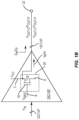
Claims (13)

  1. An asymmetrical power amplifier circuit comprising:
    a signal input configured to receive a radio frequency (RF) signal in a time-variant input power;
    a signal output configured to output the RF signal in a time-variant output power that equals a sum of a carrier output power and a peak output power;
    a carrier amplifier configured to amplify the RF signal from the time-variant input power to the carrier output power based on a modulated voltage;
    a peak amplifier configured to amplify the RF signal from the time-variant input power to the peak output power based on the modulated voltage; and
    an impedance control circuit coupled to the carrier amplifier and the peak amplifier and configured to cause the carrier output power to be different from the peak output power at a peak of the time-variant output power of the RF signal.
  2. The asymmetrical power amplifier circuit of claim 1, wherein the impedance control circuit is further configured to cause the carrier output power to be higher than the peak output power at the peak of the time-variant output power of the RF signal.
  3. The asymmetrical power amplifier circuit of claim 2, wherein the impedance control circuit is further configured to modulate a carrier impedance seen by the carrier amplifier to be different from a peak impedance seen by the peak amplifier to thereby cause the carrier output power to be different from the peak output power.
  4. The asymmetrical power amplifier circuit of claim 3, wherein the impedance control circuit is further configured to modulate the carrier impedance to be lower than the peak impedance to thereby cause the carrier output power to be higher than the peak output power.
  5. The asymmetrical power amplifier circuit of claim 3 or 4, wherein the impedance control circuit comprises a transformer comprising an input coil and an output coil, the input coil comprising:
    a center node configured to receive the modulated voltage;
    a pair of inner nodes configured to modulate the carrier impedance seen by the carrier amplifier; and
    a pair of outer nodes configured to modulate the peak impedance seen by the peak amplifier.
  6. The asymmetrical power amplifier circuit of any preceding claim, further comprising a control circuit configured to:
    activate the peak amplifier in response to the time-variant output power of the RF signal being higher than or equal to a predefined power threshold; and
    deactivate the peak amplifier in response to the time-variant output power of the RF signal being lower than the predefined power threshold.
  7. The asymmetrical power amplifier circuit of claim 6, wherein the control circuit is further configured to determine the time-variant output power of the RF signal based on at least one of: the modulated voltage, the time-variant input power of the RF signal, and an externally generated indication signal.
  8. The asymmetrical power amplifier circuit of claim 6 or 7, wherein the predefined power threshold is higher than the peak of the time-variant output power minus six decibels (6 dB).
  9. The asymmetrical power amplifier circuit of claim 6, 7 or 8, wherein:
    the carrier output power is a function of a modulated carrier voltage at a respective collector of the carrier amplifier;
    the peak output power is a function of a modulated peak voltage at a respective collector of the peak amplifier; and
    the modulated carrier voltage and the modulated peak voltage are each proportionally related to the modulated voltage.
  10. The asymmetrical power amplifier circuit of claim 9, wherein the carrier amplifier is further configured to:
    increase the modulated carrier voltage at a first rate before the peak amplifier is activated; and
    increase the modulated carrier voltage at a second rate slower than the first rate after the peak amplifier is activated.
  11. The asymmetrical power amplifier circuit of claim 10, wherein the modulated carrier voltage is equal to the modulated peak voltage at the peak of the time-variant output power of the RF signal.
  12. A wireless communication circuit comprising:
    a transceiver circuit configured to generate a radio frequency (RF) signal in a time-variant input power; and
    the asymmetrical power amplifier circuit of any preceding claim.
  13. The wireless communication circuit of claim 12, further comprising a power management integrated circuit (PMIC) configured to generate the modulated voltage.
EP23171932.9A 2022-05-12 2023-05-05 Asymmetrical power amplifier circuit Pending EP4277123A1 (en)

Applications Claiming Priority (2)

Application Number Priority Date Filing Date Title
US202263341127P 2022-05-12 2022-05-12
US18/295,990 US12587138B2 (en) 2022-05-12 2023-04-05 Asymmetrical power amplifier circuit

Publications (1)

Publication Number Publication Date
EP4277123A1 true EP4277123A1 (en) 2023-11-15

Family

ID=86330149

Family Applications (1)

Application Number Title Priority Date Filing Date
EP23171932.9A Pending EP4277123A1 (en) 2022-05-12 2023-05-05 Asymmetrical power amplifier circuit

Country Status (2)

Country Link
US (1) US12587138B2 (en)
EP (1) EP4277123A1 (en)

Cited By (2)

* Cited by examiner, † Cited by third party
Publication number Priority date Publication date Assignee Title
WO2026054938A1 (en) * 2024-09-05 2026-03-12 Qorvo Us, Inc. Operating a power management circuit based on modulation bandwidth and power backoff
WO2026054939A1 (en) * 2024-09-05 2026-03-12 Qorvo Us, Inc. Reducing supply voltage range in a power management circuit

Citations (1)

* Cited by examiner, † Cited by third party
Publication number Priority date Publication date Assignee Title
US20200350866A1 (en) * 2019-03-25 2020-11-05 Skyworks Solutions, Inc. Envelope tracking for doherty power amplifiers

Family Cites Families (19)

* Cited by examiner, † Cited by third party
Publication number Priority date Publication date Assignee Title
US20020146993A1 (en) 2001-04-04 2002-10-10 Charles Persico Bias adjustment for power amplifier
KR100553252B1 (en) * 2002-02-01 2006-02-20 아바고테크놀로지스코리아 주식회사 Power amplifier of portable terminal
KR20100069454A (en) * 2008-12-16 2010-06-24 삼성전자주식회사 Method and apparatus for enhancing performance of a doherty power amplifier in a communication system
US9531327B2 (en) * 2012-10-31 2016-12-27 Nec Corporation Power amplifier and power amplification method
JP2014175760A (en) * 2013-03-07 2014-09-22 Japan Radio Co Ltd Asymmetric Doherty power amplifier
KR101500570B1 (en) * 2013-06-26 2015-03-09 주식회사 인스파워 Asymmetric Doherty Amplifier
US9225291B2 (en) * 2013-10-29 2015-12-29 Freescale Semiconductor, Inc. Adaptive adjustment of power splitter
US9252722B2 (en) * 2013-12-20 2016-02-02 Telefonaktiebolaget L M Ericsson (Publ) Enhanced and versatile N-way doherty power amplifier
US9419561B2 (en) 2014-04-09 2016-08-16 Qualcomm, Incorporated Circuits and methods for biasing a power amplifier
US9438186B2 (en) 2014-04-30 2016-09-06 Freescale Semiconductor, Inc. Power amplifier with envelope injection
CN111313841B (en) * 2014-12-18 2023-09-12 株式会社东芝 Doherty type amplifier
US9979352B2 (en) 2016-03-02 2018-05-22 Qualcomm Incorporated Systems and methods for linearizing operation of a power amplifier
JP2018137566A (en) * 2017-02-21 2018-08-30 株式会社村田製作所 Power amplifier circuit
CN114430884B (en) * 2019-10-02 2024-11-12 三菱电机株式会社 Doherty Amplifier
US20210167735A1 (en) * 2019-12-02 2021-06-03 Nxp Usa, Inc. Doherty power amplifiers with improved peaking amplifier matching
JP7019882B2 (en) * 2019-12-13 2022-02-15 三菱電機株式会社 Doherty amplifier and communication equipment
JP2021192476A (en) 2020-06-05 2021-12-16 株式会社村田製作所 Power amplifier circuit
US11190147B1 (en) 2020-06-18 2021-11-30 Silicon Laboratories Inc. Low power, efficient doherty power amplifier
US12413190B2 (en) * 2021-08-16 2025-09-09 Skyworks Solutions, Inc. Power amplifier supply networks with harmonic terminations

Patent Citations (1)

* Cited by examiner, † Cited by third party
Publication number Priority date Publication date Assignee Title
US20200350866A1 (en) * 2019-03-25 2020-11-05 Skyworks Solutions, Inc. Envelope tracking for doherty power amplifiers

Non-Patent Citations (2)

* Cited by examiner, † Cited by third party
Title
JOON HYUNG KIM ET AL: "Analysis and Implementation of Doherty Power Amplifier With Two-Point Envelope Modulation", IEEE TRANSACTIONS ON MICROWAVE THEORY AND TECHNIQUES, IEEE, USA, vol. 60, no. 5, 1 May 2012 (2012-05-01), pages 1353 - 1364, XP011442428, ISSN: 0018-9480, DOI: 10.1109/TMTT.2012.2188725 *
RAMZI DARRAJI ET AL: "Mitigation of Bandwidth Limitation in Wireless Doherty Amplifiers With Substantial Bandwidth Enhancement Using Digital Techniques", IEEE TRANSACTIONS ON MICROWAVE THEORY AND TECHNIQUES, IEEE, USA, vol. 60, no. 9, 1 September 2012 (2012-09-01), pages 2875 - 2885, XP011458841, ISSN: 0018-9480, DOI: 10.1109/TMTT.2012.2207910 *

Cited By (2)

* Cited by examiner, † Cited by third party
Publication number Priority date Publication date Assignee Title
WO2026054938A1 (en) * 2024-09-05 2026-03-12 Qorvo Us, Inc. Operating a power management circuit based on modulation bandwidth and power backoff
WO2026054939A1 (en) * 2024-09-05 2026-03-12 Qorvo Us, Inc. Reducing supply voltage range in a power management circuit

Also Published As

Publication number Publication date
US12587138B2 (en) 2026-03-24
US20230370021A1 (en) 2023-11-16

Similar Documents

Publication Publication Date Title
US10187137B2 (en) High power user equipment (HPUE) using coherently combined power amplifiers
EP4277123A1 (en) Asymmetrical power amplifier circuit
US20250105790A1 (en) Voltage ripple cancellation in a transmission circuit
US20250253882A1 (en) Transceiver circuit operable in a dynamic power range
US12244275B2 (en) Radio frequency signal phase correction in power amplifier circuit
CN106416089A (en) Reduce power consumption at the transceiver
KR102461243B1 (en) Differential cascode amplifier with selectively coupled gate terminals
CN117060859A (en) Asymmetric power amplifier circuit
US8320855B2 (en) Probability optimized power amplifier module and transmitter
US20230261614A1 (en) Amplifier system
US8817852B2 (en) Communication apparatuses and radio frequency equalizers
US20250239977A1 (en) Loadline modulation power management circuit
US20250062729A1 (en) Efficiency improvement in a wireless transmission circuit
US20250105791A1 (en) Multi-transmission envelope tracking circuit
US20260058612A1 (en) Interfacing methods in a power management circuit
HK40096527A (en) Asymmetrical power amplifier circuit
US20260058605A1 (en) Dynamic impedance modulation in a power management circuit
CN119698758A (en) Power Management Circuit
US20260088773A1 (en) Power amplifier efficiency and linearity in a wireless transmission circuit
US20240243700A1 (en) Methods and techniques to achieve target phase shift over wide frequency band in the input of doherty power amplifiers
WO2026024380A1 (en) Controlling a dual-amplifier power amplifier circuit in a power management circuit
US20260051853A1 (en) Power management circuit operable with a reduced voltage range
US12549138B1 (en) Bandwidth adaptation in a transmission circuit
CN118975123A (en) Transceiver circuits that can operate within a dynamic power range
WO2024145101A1 (en) Power distributor circuits for load modulated amplifiers

Legal Events

Date Code Title Description
PUAI Public reference made under article 153(3) epc to a published international application that has entered the european phase

Free format text: ORIGINAL CODE: 0009012

STAA Information on the status of an ep patent application or granted ep patent

Free format text: STATUS: THE APPLICATION HAS BEEN PUBLISHED

AK Designated contracting states

Kind code of ref document: A1

Designated state(s): AL AT BE BG CH CY CZ DE DK EE ES FI FR GB GR HR HU IE IS IT LI LT LU LV MC ME MK MT NL NO PL PT RO RS SE SI SK SM TR

STAA Information on the status of an ep patent application or granted ep patent

Free format text: STATUS: REQUEST FOR EXAMINATION WAS MADE

17P Request for examination filed

Effective date: 20240510

RBV Designated contracting states (corrected)

Designated state(s): AL AT BE BG CH CY CZ DE DK EE ES FI FR GB GR HR HU IE IS IT LI LT LU LV MC ME MK MT NL NO PL PT RO RS SE SI SK SM TR