EP4276888A1 - Method for producing a power semiconductor module - Google Patents
Method for producing a power semiconductor module Download PDFInfo
- Publication number
- EP4276888A1 EP4276888A1 EP22172217.6A EP22172217A EP4276888A1 EP 4276888 A1 EP4276888 A1 EP 4276888A1 EP 22172217 A EP22172217 A EP 22172217A EP 4276888 A1 EP4276888 A1 EP 4276888A1
- Authority
- EP
- European Patent Office
- Prior art keywords
- liquid
- semi
- lid
- sidewalls
- substrate
- Prior art date
- Legal status (The legal status is an assumption and is not a legal conclusion. Google has not performed a legal analysis and makes no representation as to the accuracy of the status listed.)
- Pending
Links
Images


Classifications
-
- H—ELECTRICITY
- H10—SEMICONDUCTOR DEVICES; ELECTRIC SOLID-STATE DEVICES NOT OTHERWISE PROVIDED FOR
- H10W—GENERIC PACKAGES, INTERCONNECTIONS, CONNECTORS OR OTHER CONSTRUCTIONAL DETAILS OF DEVICES COVERED BY CLASS H10
- H10W76/00—Containers; Fillings or auxiliary members therefor; Seals
- H10W76/10—Containers or parts thereof
- H10W76/12—Containers or parts thereof characterised by their shape
- H10W76/15—Containers comprising an insulating or insulated base
-
- H—ELECTRICITY
- H10—SEMICONDUCTOR DEVICES; ELECTRIC SOLID-STATE DEVICES NOT OTHERWISE PROVIDED FOR
- H10W—GENERIC PACKAGES, INTERCONNECTIONS, CONNECTORS OR OTHER CONSTRUCTIONAL DETAILS OF DEVICES COVERED BY CLASS H10
- H10W70/00—Package substrates; Interposers; Redistribution layers [RDL]
- H10W70/60—Insulating or insulated package substrates; Interposers; Redistribution layers
-
- H—ELECTRICITY
- H10—SEMICONDUCTOR DEVICES; ELECTRIC SOLID-STATE DEVICES NOT OTHERWISE PROVIDED FOR
- H10W—GENERIC PACKAGES, INTERCONNECTIONS, CONNECTORS OR OTHER CONSTRUCTIONAL DETAILS OF DEVICES COVERED BY CLASS H10
- H10W72/00—Interconnections or connectors in packages
- H10W72/071—Connecting or disconnecting
-
- H—ELECTRICITY
- H10—SEMICONDUCTOR DEVICES; ELECTRIC SOLID-STATE DEVICES NOT OTHERWISE PROVIDED FOR
- H10W—GENERIC PACKAGES, INTERCONNECTIONS, CONNECTORS OR OTHER CONSTRUCTIONAL DETAILS OF DEVICES COVERED BY CLASS H10
- H10W74/00—Encapsulations, e.g. protective coatings
- H10W74/01—Manufacture or treatment
- H10W74/016—Manufacture or treatment using moulds
-
- H—ELECTRICITY
- H10—SEMICONDUCTOR DEVICES; ELECTRIC SOLID-STATE DEVICES NOT OTHERWISE PROVIDED FOR
- H10W—GENERIC PACKAGES, INTERCONNECTIONS, CONNECTORS OR OTHER CONSTRUCTIONAL DETAILS OF DEVICES COVERED BY CLASS H10
- H10W76/00—Containers; Fillings or auxiliary members therefor; Seals
- H10W76/10—Containers or parts thereof
- H10W76/12—Containers or parts thereof characterised by their shape
-
- H—ELECTRICITY
- H10—SEMICONDUCTOR DEVICES; ELECTRIC SOLID-STATE DEVICES NOT OTHERWISE PROVIDED FOR
- H10W—GENERIC PACKAGES, INTERCONNECTIONS, CONNECTORS OR OTHER CONSTRUCTIONAL DETAILS OF DEVICES COVERED BY CLASS H10
- H10W76/00—Containers; Fillings or auxiliary members therefor; Seals
- H10W76/40—Fillings or auxiliary members in containers, e.g. centering rings
- H10W76/42—Fillings
- H10W76/47—Solid or gel fillings
-
- H—ELECTRICITY
- H10—SEMICONDUCTOR DEVICES; ELECTRIC SOLID-STATE DEVICES NOT OTHERWISE PROVIDED FOR
- H10W—GENERIC PACKAGES, INTERCONNECTIONS, CONNECTORS OR OTHER CONSTRUCTIONAL DETAILS OF DEVICES COVERED BY CLASS H10
- H10W76/00—Containers; Fillings or auxiliary members therefor; Seals
- H10W76/60—Seals
-
- H—ELECTRICITY
- H10—SEMICONDUCTOR DEVICES; ELECTRIC SOLID-STATE DEVICES NOT OTHERWISE PROVIDED FOR
- H10W—GENERIC PACKAGES, INTERCONNECTIONS, CONNECTORS OR OTHER CONSTRUCTIONAL DETAILS OF DEVICES COVERED BY CLASS H10
- H10W95/00—Packaging processes not covered by the other groups of this subclass
-
- H—ELECTRICITY
- H10—SEMICONDUCTOR DEVICES; ELECTRIC SOLID-STATE DEVICES NOT OTHERWISE PROVIDED FOR
- H10W—GENERIC PACKAGES, INTERCONNECTIONS, CONNECTORS OR OTHER CONSTRUCTIONAL DETAILS OF DEVICES COVERED BY CLASS H10
- H10W40/00—Arrangements for thermal protection or thermal control
- H10W40/20—Arrangements for cooling
- H10W40/25—Arrangements for cooling characterised by their materials
- H10W40/255—Arrangements for cooling characterised by their materials having a laminate or multilayered structure, e.g. direct bond copper [DBC] ceramic substrates
-
- H—ELECTRICITY
- H10—SEMICONDUCTOR DEVICES; ELECTRIC SOLID-STATE DEVICES NOT OTHERWISE PROVIDED FOR
- H10W—GENERIC PACKAGES, INTERCONNECTIONS, CONNECTORS OR OTHER CONSTRUCTIONAL DETAILS OF DEVICES COVERED BY CLASS H10
- H10W72/00—Interconnections or connectors in packages
- H10W72/071—Connecting or disconnecting
- H10W72/073—Connecting or disconnecting of die-attach connectors
- H10W72/07331—Connecting techniques
-
- H—ELECTRICITY
- H10—SEMICONDUCTOR DEVICES; ELECTRIC SOLID-STATE DEVICES NOT OTHERWISE PROVIDED FOR
- H10W—GENERIC PACKAGES, INTERCONNECTIONS, CONNECTORS OR OTHER CONSTRUCTIONAL DETAILS OF DEVICES COVERED BY CLASS H10
- H10W72/00—Interconnections or connectors in packages
- H10W72/30—Die-attach connectors
- H10W72/321—Structures or relative sizes of die-attach connectors
- H10W72/325—Die-attach connectors having a filler embedded in a matrix
-
- H—ELECTRICITY
- H10—SEMICONDUCTOR DEVICES; ELECTRIC SOLID-STATE DEVICES NOT OTHERWISE PROVIDED FOR
- H10W—GENERIC PACKAGES, INTERCONNECTIONS, CONNECTORS OR OTHER CONSTRUCTIONAL DETAILS OF DEVICES COVERED BY CLASS H10
- H10W72/00—Interconnections or connectors in packages
- H10W72/30—Die-attach connectors
- H10W72/351—Materials of die-attach connectors
- H10W72/352—Materials of die-attach connectors comprising metals or metalloids, e.g. solders
-
- H—ELECTRICITY
- H10—SEMICONDUCTOR DEVICES; ELECTRIC SOLID-STATE DEVICES NOT OTHERWISE PROVIDED FOR
- H10W—GENERIC PACKAGES, INTERCONNECTIONS, CONNECTORS OR OTHER CONSTRUCTIONAL DETAILS OF DEVICES COVERED BY CLASS H10
- H10W72/00—Interconnections or connectors in packages
- H10W72/30—Die-attach connectors
- H10W72/351—Materials of die-attach connectors
- H10W72/353—Materials of die-attach connectors not comprising solid metals or solid metalloids, e.g. ceramics
- H10W72/354—Materials of die-attach connectors not comprising solid metals or solid metalloids, e.g. ceramics comprising polymers
-
- H—ELECTRICITY
- H10—SEMICONDUCTOR DEVICES; ELECTRIC SOLID-STATE DEVICES NOT OTHERWISE PROVIDED FOR
- H10W—GENERIC PACKAGES, INTERCONNECTIONS, CONNECTORS OR OTHER CONSTRUCTIONAL DETAILS OF DEVICES COVERED BY CLASS H10
- H10W72/00—Interconnections or connectors in packages
- H10W72/50—Bond wires
- H10W72/531—Shapes of wire connectors
- H10W72/5363—Shapes of wire connectors the connected ends being wedge-shaped
-
- H—ELECTRICITY
- H10—SEMICONDUCTOR DEVICES; ELECTRIC SOLID-STATE DEVICES NOT OTHERWISE PROVIDED FOR
- H10W—GENERIC PACKAGES, INTERCONNECTIONS, CONNECTORS OR OTHER CONSTRUCTIONAL DETAILS OF DEVICES COVERED BY CLASS H10
- H10W72/00—Interconnections or connectors in packages
- H10W72/50—Bond wires
- H10W72/551—Materials of bond wires
-
- H—ELECTRICITY
- H10—SEMICONDUCTOR DEVICES; ELECTRIC SOLID-STATE DEVICES NOT OTHERWISE PROVIDED FOR
- H10W—GENERIC PACKAGES, INTERCONNECTIONS, CONNECTORS OR OTHER CONSTRUCTIONAL DETAILS OF DEVICES COVERED BY CLASS H10
- H10W72/00—Interconnections or connectors in packages
- H10W72/851—Dispositions of multiple connectors or interconnections
- H10W72/874—On different surfaces
- H10W72/884—Die-attach connectors and bond wires
-
- H—ELECTRICITY
- H10—SEMICONDUCTOR DEVICES; ELECTRIC SOLID-STATE DEVICES NOT OTHERWISE PROVIDED FOR
- H10W—GENERIC PACKAGES, INTERCONNECTIONS, CONNECTORS OR OTHER CONSTRUCTIONAL DETAILS OF DEVICES COVERED BY CLASS H10
- H10W74/00—Encapsulations, e.g. protective coatings
-
- H—ELECTRICITY
- H10—SEMICONDUCTOR DEVICES; ELECTRIC SOLID-STATE DEVICES NOT OTHERWISE PROVIDED FOR
- H10W—GENERIC PACKAGES, INTERCONNECTIONS, CONNECTORS OR OTHER CONSTRUCTIONAL DETAILS OF DEVICES COVERED BY CLASS H10
- H10W76/00—Containers; Fillings or auxiliary members therefor; Seals
- H10W76/01—Manufacture or treatment
- H10W76/05—Providing fillings in containers, e.g. gas filling
-
- H—ELECTRICITY
- H10—SEMICONDUCTOR DEVICES; ELECTRIC SOLID-STATE DEVICES NOT OTHERWISE PROVIDED FOR
- H10W—GENERIC PACKAGES, INTERCONNECTIONS, CONNECTORS OR OTHER CONSTRUCTIONAL DETAILS OF DEVICES COVERED BY CLASS H10
- H10W76/00—Containers; Fillings or auxiliary members therefor; Seals
- H10W76/10—Containers or parts thereof
- H10W76/12—Containers or parts thereof characterised by their shape
- H10W76/15—Containers comprising an insulating or insulated base
- H10W76/157—Containers comprising an insulating or insulated base having interconnections parallel to the insulating or insulated base
-
- H—ELECTRICITY
- H10—SEMICONDUCTOR DEVICES; ELECTRIC SOLID-STATE DEVICES NOT OTHERWISE PROVIDED FOR
- H10W—GENERIC PACKAGES, INTERCONNECTIONS, CONNECTORS OR OTHER CONSTRUCTIONAL DETAILS OF DEVICES COVERED BY CLASS H10
- H10W76/00—Containers; Fillings or auxiliary members therefor; Seals
- H10W76/10—Containers or parts thereof
- H10W76/17—Containers or parts thereof characterised by their materials
-
- H—ELECTRICITY
- H10—SEMICONDUCTOR DEVICES; ELECTRIC SOLID-STATE DEVICES NOT OTHERWISE PROVIDED FOR
- H10W—GENERIC PACKAGES, INTERCONNECTIONS, CONNECTORS OR OTHER CONSTRUCTIONAL DETAILS OF DEVICES COVERED BY CLASS H10
- H10W90/00—Package configurations
-
- H—ELECTRICITY
- H10—SEMICONDUCTOR DEVICES; ELECTRIC SOLID-STATE DEVICES NOT OTHERWISE PROVIDED FOR
- H10W—GENERIC PACKAGES, INTERCONNECTIONS, CONNECTORS OR OTHER CONSTRUCTIONAL DETAILS OF DEVICES COVERED BY CLASS H10
- H10W90/00—Package configurations
- H10W90/701—Package configurations characterised by the relative positions of pads or connectors relative to package parts
-
- H—ELECTRICITY
- H10—SEMICONDUCTOR DEVICES; ELECTRIC SOLID-STATE DEVICES NOT OTHERWISE PROVIDED FOR
- H10W—GENERIC PACKAGES, INTERCONNECTIONS, CONNECTORS OR OTHER CONSTRUCTIONAL DETAILS OF DEVICES COVERED BY CLASS H10
- H10W90/00—Package configurations
- H10W90/701—Package configurations characterised by the relative positions of pads or connectors relative to package parts
- H10W90/731—Package configurations characterised by the relative positions of pads or connectors relative to package parts of die-attach connectors
- H10W90/734—Package configurations characterised by the relative positions of pads or connectors relative to package parts of die-attach connectors between a chip and a stacked insulating package substrate, interposer or RDL
-
- H—ELECTRICITY
- H10—SEMICONDUCTOR DEVICES; ELECTRIC SOLID-STATE DEVICES NOT OTHERWISE PROVIDED FOR
- H10W—GENERIC PACKAGES, INTERCONNECTIONS, CONNECTORS OR OTHER CONSTRUCTIONAL DETAILS OF DEVICES COVERED BY CLASS H10
- H10W90/00—Package configurations
- H10W90/701—Package configurations characterised by the relative positions of pads or connectors relative to package parts
- H10W90/751—Package configurations characterised by the relative positions of pads or connectors relative to package parts of bond wires
- H10W90/754—Package configurations characterised by the relative positions of pads or connectors relative to package parts of bond wires between a chip and a stacked insulating package substrate, interposer or RDL
Definitions
- the instant disclosure relates to a method for producing a power semiconductor module, in particular to a method for producing a power semiconductor module comprising a casting compound.
- Power semiconductor modules often include a substrate arranged in a housing.
- a semiconductor arrangement including a plurality of controllable semiconductor elements may be arranged on the substrate.
- the substrate usually comprises a substrate layer (e.g., a ceramic layer), a first metallization layer deposited on a first side of the substrate layer and a second metallization layer deposited on a second side of the substrate layer.
- the controllable semiconductor elements are mounted, for example, on the first metallization layer.
- the housing may be partly filled with a casting compound to protect the components and electrical connections inside the power semiconductor module, in particular inside the housing, from certain environmental conditions, mechanical damage and insulation faults.
- a casting compound usually a liquid, semi-liquid or viscous material is poured into the housing, thereby forming a liquid or viscous pre-layer.
- a heating step may follow during which liquid that is present in the pre-layer is at least partly evaporated. In this way, the pre-layer is hardened to form the resulting casting compound.
- a lid of the housing is wetted by the material of the casting compound during the heating step. The material may then unintentionally leak out of the housing.
- a method includes pouring a liquid, semi-liquid or viscous material into a cavity formed by sidewalls of a housing, thereby covering a substrate that is arranged in the cavity formed by the sidewalls, arranging a lid on the sidewalls, thereby covering the cavity formed by the sidewalls, wherein the lid comprises at least one functional element that extends from the lid into the liquid, semi-liquid or viscous material in a direction towards the substrate once the lid is in its final mounting position, and curing the liquid, semi-liquid or viscous material in order to form a casting compound.
- An electrical line or electrical connection as described herein may be a single electrically conductive element, or may include at least two individual electrically conductive elements connected in series and/or parallel. Electrical lines and electrical connections may include metal and/or semiconductor material, and may be permanently electrically conductive (i.e., non-switchable).
- a semiconductor body as described herein may be made from (doped) semiconductor material and may be a semiconductor chip or may be included in a semiconductor chip.
- a semiconductor body has electrically connecting pads and includes at least one semiconductor element with electrodes.
- the power semiconductor module includes a housing and a substrate 10.
- the substrate 10 includes a dielectric insulation layer 11, a (structured) first metallization layer 111 attached to the dielectric insulation layer 11, and a second (structured) metallization layer 112 attached to the dielectric insulation layer 11.
- the dielectric insulation layer 11 is disposed between the first and second metallization layers 111, 112. It is, however, also possible that the substrate 10 only comprises a first metallization layer 111, and that the second metallization layer 112 is omitted.
- Each of the first and second metallization layers 111, 112 may consist of or include one of the following materials: copper; a copper alloy; aluminum; an aluminum alloy; any other metal or alloy that remains solid during the operation of the power semiconductor module arrangement.
- the substrate 10 may be a ceramic substrate, that is, a substrate in which the dielectric insulation layer 11 is a ceramic, e.g., a thin ceramic layer.
- the ceramic may consist of or include one of the following materials: aluminum oxide; aluminum nitride; zirconium oxide; silicon nitride; boron nitride; or any other dielectric ceramic.
- the dielectric insulation layer 11 may consist of or include one of the following materials: Al 2 O 3 , AlN, SiC, BeO or Si 3 N 4 .
- the substrate 10 may be, e.g., a Direct Copper Bonding (DCB) substrate, a Direct Aluminum Bonding (DAB) substrate, or an Active Metal Brazing (AMB) substrate.
- the substrate 10 may be an Insulated Metal Substrate (IMS).
- An Insulated Metal Substrate generally comprises a dielectric insulation layer 11 comprising (filled) materials such as epoxy resin or polyimide, for example.
- the material of the dielectric insulation layer 11 may be filled with ceramic particles, for example. Such particles may comprise, e.g., SiO 2 , Al 2 O 3 , AlN, or BN and may have a diameter of between about 1 ⁇ m and about 50 ⁇ m.
- the substrate 10 may also be a conventional printed circuit board (PCB) having a non-ceramic dielectric insulation layer 11.
- a non-ceramic dielectric insulation layer 11 may consist of or include a cured resin.
- the substrate 10 is arranged in a housing.
- the substrate 10 is arranged on a ground surface 12 of the housing.
- the housing further comprises sidewalls 42 and a lid 44.
- the sidewalls 42 and the lid 44 are separate elements. That is, when assembling the power semiconductor module arrangement, the sidewalls 42 may be arranged on the substrate and/or the ground surface 12 first, with the lid still being open.
- the lid 44 may only be mounted on the sidewalls 42 at a later stage during the assembly.
- the ground surface 12 of the housing may be omitted. In such cases the substrate 10 itself may form the ground surface of the housing.
- the substrate 10 may also be arranged on a base plate or heat sink 12, for example.
- the ground surface 12, the sidewalls 42 and the lid 44 may include a metal or a metal alloy, for example. It is, however, also possible that the ground surface 12, sidewalls 42 and lid 44 comprise an electrically insulating material such as a plastic or ceramic material, for example.
- the housing may also include a liquid crystal polymer, for example. Other materials are also possible.
- the housing is rectangular or has a square shape and has four sidewalls 42. This, however, is only an example. It is generally possible that the housing comprises any number of sidewalls (e.g., three, four, or even more). The number of sidewalls is not relevant for the present invention.
- connection layer may be a solder layer, a layer of an adhesive material, or a layer of a sintered metal powder, e.g., a sintered silver powder, for example. Any other kind of electrically conducting or non-conducting connection layer is also possible.
- One or more semiconductor bodies 20 may be arranged on the substrate 10.
- Each of the semiconductor bodies 20 arranged on the substrate 10 may include a diode, an IGBT (Insulated-Gate Bipolar Transistor), a MOSFET (Metal-Oxide-Semiconductor Field-Effect Transistor), a JFET (Junction Field-Effect Transistor), a HEMT (High-Electron-Mobility Transistor), or any other suitable controllable semiconductor element.
- IGBT Insulated-Gate Bipolar Transistor
- MOSFET Metal-Oxide-Semiconductor Field-Effect Transistor
- JFET Joint Field-Effect Transistor
- HEMT High-Electron-Mobility Transistor
- the one or more semiconductor bodies 20 may form a semiconductor arrangement on the substrate 10.
- the second metallization layer 112 of the substrate 10 in Figure 1 is a continuous layer.
- the first metallization layer 111 of the example in Figure 1 is also a continuous layer.
- the first metallization layer 111, or the second metallization layer 112, or both can also be structured layers.
- Structured layer means that, e.g., the respective metallization layer 111, 112 is not a continuous layer, but includes recesses between different sections of the layer.
- Different semiconductor bodies 20 may be mounted to the same or to different sections of the first metallization layer 111.
- the first metallization layer 111 may have no electrical connection or may be electrically connected to one or more other sections using, e.g., bonding wires. Electrical connections may also include bonding ribbons, connection plates or conductor rails, for example, to name just a few examples. According to another example, the second metallization layer 112 can be omitted altogether.
- the one or more semiconductor bodies 20 may be electrically and mechanically connected to the substrate 10 by an electrically conductive connection layer 22.
- Such an electrically conductive connection layer 22 may be a solder layer, a layer of an electrically conductive adhesive, or a layer of a sintered metal powder, e.g., a sintered silver powder, for example.
- the power semiconductor module may further include terminal elements 30.
- the terminal elements 30 are electrically connected to the substrate 10, e.g., to the first metallization layer 111 of the substrate 10, and form a contact element which provides an electrical connection between the inside and the outside of the housing.
- the terminal elements 30 may extend through the housing as shown in Figures 1 and 2 , or they may be formed as part of the housing, and connected electrically to the substrate 10 via further conductors without being in direct physical contact with the substrate 10.
- a first end of the terminal elements 30 may be electrically and mechanically connected to the first metallization layer 111 by an electrically conductive connection layer (not specifically illustrated).
- Such an electrically conductive connection layer may be a solder layer, a layer of an electrically conductive adhesive, or a layer of a sintered metal powder, e.g., a sintered silver powder, for example.
- a second end of the terminal elements 30 protrudes out of the housing to allow the terminal element 30 to be electrically contacted from the outside.
- the lid 44 may comprise through holes or openings through which the terminal elements 30 may protrude such that their first end is inside the housing and their second end is outside the housing.
- the terminal elements 30 may protrude vertically (i.e., perpendicular to a top surface of the substrate 10) out of the housing when the housing is arranged to surround the substrate 10. According to another example, terminal elements 30 may also protrude horizontally (parallel to the top surface of the substrate 10) through a sidewall 42 of the housing.
- the semiconductor module arrangement illustrated in Figure 1 further comprises press-on pins 48.
- the press-on pins 48 are attached to the lid 44 and extend vertically from the lid 44 towards the substrate 10.
- the press-on pins 48 contact the substrate 10, for example.
- the press-on pins 48 are illustrated as being arranged at a certain distance from the different semiconductor bodies 20 in a horizontal direction x. This, however, is only an example.
- press-on pins 48 may also be arranged in close vicinity to at least one of the semiconductor bodies 20.
- press-on pins 48 may contact a semiconductor body 20 instead of on the substrate 10. If the press-on pin 48 contacts a semiconductor body 20, the respective semiconductor body 20 is arranged between the press-on pin 48 and the substrate 10.
- the press-on pin 48 may be arranged at a central position within the housing. That is, the press-on pin 48 may be arranged at a first distance from a first sidewall and at a second distance from a second sidewall opposite the first sidewall, wherein the first distance equals the second distance, and at a third distance from a third sidewall and at a fourth distance from a fourth sidewall opposite the third sidewall, wherein the third distance equals the fourth distance. Press-on pins, however, may also be arranged at any other suitable position within the housing.
- the substrate 10 When the semiconductor module arrangement is fully assembled, the substrate 10 is pressed onto the ground surface 12 of the housing by means of the press-on pins 48 in order to reduce a thermal resistance between the substrate 10 and the ground surface 12. Further, the substrate 10 is thereby kept in a desired position and is prevented from shifting inside the housing.
- the press-on pins 48 contact the substrate 10 or one of the semiconductor bodies 20 and exert a pressure on the press-on pins 48.
- the bold arrows in Figure 1 illustrate a direction in which the lid 44 is moved while closing the housing and a direction of the pressure exerted on the press-on pin 48 once the housing is fully closed.
- the power semiconductor module arrangement comprises a plurality of terminal elements 30 and a plurality of press-on pins 48.
- a power semiconductor module arrangement may comprise at least one functional element, the at least one functional element comprising at least one terminal element and/or at least one press-on pin 48.
- the term "functional element” as used herein refers to any element extending from the lid 44 of the housing in a vertical direction towards the substrate 10 that exhibits at least one specific function within the power semiconductor module arrangement.
- the terminal elements for example, fall under the term functional element as they are configured to conduct currents / voltages and to transmit signals between the inside and the outside of the housing.
- the press-on pins 48 are used to press the substrate 10 towards the ground surface 12, and are therefore functional elements. There may be, however, any other kinds of functional elements that exhibit other functions and that extend from the lid 44 towards the substrate 10. Such functional elements do not necessarily extend all the way towards the substrate. It is generally also possible that a functional element does not directly contact the substrate 10 or any of the elements mounted thereon.
- the casting compound 5 may consist of or include a silicone gel or may be a rigid molding compound, for example.
- the casting compound 5 may partly fill the interior of the housing, thereby covering the substrate 10 and the semiconductor bodies 20, and any other components and electrical connections 24 that are arranged on the substrate 10.
- Electrical connections 24 such as, e.g., bonding wires or bonding ribbons, may electrically couple the semiconductor bodies 20 to the first metallization layer 111, to other semiconductor bodies 20, or to any other components that may be arranged inside the housing.
- the terminal elements 30 may be partly embedded in the casting compound 5. At least the second ends of the terminal elements 30, however, may not be covered by the casting compound 5 and may protrude from the casting compound 5. The same applies for the press-on pins 48.
- the casting compound 5 is configured to protect the components and electrical connections inside the power semiconductor module arrangement, in particular inside the housing, from certain environmental conditions, mechanical damage and insulation faults.
- a liquid, semi-liquid or viscous material is poured into the housing, thereby forming a liquid, semi-liquid or viscous pre-layer.
- the lid 44 is already arranged on the sidewalls 42 at this point.
- the lid 44 may comprise an opening through which the liquid, semi-liquid or viscous material may be poured into the housing.
- a heating step may follow during which liquid that is present in the pre-layer is at least partly evaporated. In this way, the pre-layer is hardened to form the resulting casting compound 5.
- the liquid, semi-liquid or viscous material is generally poured into the housing at room temperature.
- the liquid, semi-liquid or viscous material is heated to temperatures of up to 120°C or even more.
- the liquid, semi-liquid or viscous material of the pre-layer may be heated to temperatures of between 60°C and 120°C.
- heat is applied to the liquid, semi-liquid or viscous material of the casting compound 5
- liquid that is present in the pre-layer evaporates and a cross-linking process is started. After a certain time, e.g., 10 to 20 minutes, the material is sufficiently cured, thereby forming the resulting casting compound 5.
- the liquid, semi-liquid or viscous material expands to a certain degree, due to the high temperatures.
- certain functional elements such as, e.g., the terminal elements 30 or the press-on pins 48, extend from the lid 44 of the housing toward the substrate 10. A part of such functional elements, therefore, is embedded in the liquid, semi-liquid or viscous material of the pre-layer, while another part of the functional elements extends out of the liquid, semi-liquid or viscous material and further towards the lid 44. This may be the case for other functional elements of the power semiconductor module as well.
- the material creeps along such functional elements in a vertical direction y to the inner surface of the lid 44, the inner surface of the lid 44 being a surface facing towards the substrate 10.
- the inner surface of the lid 44 may be wetted by the material of the pre-layer. If a certain amount of material collects on the inner surface of the lid 44, it may further creep along the lid 44 towards the sidewalls 42. There it may unintentionally leak out of the housing, especially at the beginning of the heating step when the material is not yet sufficiently cross-linked and hardened.
- the leaking of material out of the housing is schematically illustrated in the arrangement illustrated in Figure 3 .
- the material wetting the lid 44 and leaking out of the housing may negatively affect the performance and the lifetime of the power semiconductor module.
- the liquid, semi-liquid or viscous material of the pre-layer is filled into the housing first, and only then the lid 44 is arranged on the sidewalls 42.
- the lid 44 is arranged on the sidewalls 42 before hardening the liquid, semi-liquid or viscous material of the pre-layer.
- the functional elements therefore, are immersed into the liquid, semi-liquid or viscous material of the pre-layer while mounting the lid 44 on the sidewalls 42.
- the functional elements displace the liquid, semi-liquid or viscous material of the pre-layer to a certain degree. That is, after mounting the lid 44 on the sidewalls, a height of the liquid, semi-liquid or viscous material of the pre-layer in the vertical direction y above the substrate 10 increases to a certain degree.
- the increase in height may be marginal, if there are only few functional elements and/or only small functional elements of comparably small volume.
- the increase in height may be somewhat more if there are many functional elements and/or large functional elements of a larger volume.
- the effect of material creeping along the functional elements toward the inner surface of the lid 44 and from there leaking out of the housing may be significantly reduced or even completely prevented.
- the vertical insertion of the functional elements into the liquid, semi-liquid or viscous material of the pre-layer has significant influence on the capillary or any other effects.
- the substrate 10 (with semiconductor bodies 20 and other elements and components mounted thereon) is arranged on a ground surface 12.
- the sidewalls 42 are arranged to surround the substrate 10.
- the liquid, semi-liquid or viscous material of the pre-layer is filled into the housing (i.e. into the cavity formed by the sidewalls 42) to cover the substrate 10 and the components mounted thereon.
- the liquid, semi-liquid or viscous material of the pre-layer does not completely fill the cavity formed by the sidewalls 42. At least part of the cavity remains free from the liquid, semi-liquid or viscous material of the pre-layer.
- the lid 44 with the functional elements attached thereto is mounted on the sidewalls 42.
- a volume that is not filled with the liquid, semi-liquid or viscous material of the pre-layer remains between the liquid, semi-liquid or viscous material of the pre-layer and the inner surface of the lid 44. That is, the inner surface of the lid 44 is not in direct contact with the liquid, semi-liquid or viscous material of the pre-layer.
- the liquid, semi-liquid or viscous material of the pre-layer is hardened/cured, thereby forming the final casting compound 5.
- the entire opening formed by the sidewalls 42 remains available during the step of filling the liquid, semi-liquid or viscous material of the pre-layer into the housing. That is, a position of a nozzle through which the liquid, semi-liquid or viscous material is injected into the housing may be freely chosen and is not restricted by a comparably small opening provided in the lid 44. It is even possible to use a plurality of nozzles at different positions. In this way, the liquid, semi-liquid or viscous material may be filled into the housing in a shorter time which results in decreased costs.
Landscapes
- Structures Or Materials For Encapsulating Or Coating Semiconductor Devices Or Solid State Devices (AREA)
Abstract
A method comprises pouring a liquid, semi-liquid or viscous material into a cavity formed by sidewalls of a housing, thereby covering a substrate that is arranged in the cavity formed by the sidewalls, arranging a lid on the sidewalls, thereby covering the cavity formed by the sidewalls, wherein the lid comprises at least one functional element that extends from the lid into the liquid, semi-liquid or viscous material in a direction towards the substrate once the lid is in its final mounting position, and curing the liquid, semi-liquid or viscous material in order to form a casting compound.
Description
- The instant disclosure relates to a method for producing a power semiconductor module, in particular to a method for producing a power semiconductor module comprising a casting compound.
- Power semiconductor modules often include a substrate arranged in a housing. A semiconductor arrangement including a plurality of controllable semiconductor elements (e.g., two IGBTs in a half-bridge configuration) may be arranged on the substrate. The substrate usually comprises a substrate layer (e.g., a ceramic layer), a first metallization layer deposited on a first side of the substrate layer and a second metallization layer deposited on a second side of the substrate layer. The controllable semiconductor elements are mounted, for example, on the first metallization layer.
- The housing may be partly filled with a casting compound to protect the components and electrical connections inside the power semiconductor module, in particular inside the housing, from certain environmental conditions, mechanical damage and insulation faults. When the casting compound is formed, usually a liquid, semi-liquid or viscous material is poured into the housing, thereby forming a liquid or viscous pre-layer. A heating step may follow during which liquid that is present in the pre-layer is at least partly evaporated. In this way, the pre-layer is hardened to form the resulting casting compound. There is a risk that a lid of the housing is wetted by the material of the casting compound during the heating step. The material may then unintentionally leak out of the housing.
- There is a need for a method for producing a semiconductor module arrangement that prevents the material of the casting compound from leaking out of the housing.
- A method includes pouring a liquid, semi-liquid or viscous material into a cavity formed by sidewalls of a housing, thereby covering a substrate that is arranged in the cavity formed by the sidewalls, arranging a lid on the sidewalls, thereby covering the cavity formed by the sidewalls, wherein the lid comprises at least one functional element that extends from the lid into the liquid, semi-liquid or viscous material in a direction towards the substrate once the lid is in its final mounting position, and curing the liquid, semi-liquid or viscous material in order to form a casting compound.
- The invention may be better understood with reference to the following drawings and the description. The components in the figures are not necessarily to scale, emphasis instead being placed upon illustrating the principles of the invention. Moreover, in the figures, like reference numerals designate corresponding parts throughout the different views.
-
-
Figure 1 is a cross-sectional view of a power semiconductor module without a casting compound. -
Figure 2 is a cross-sectional view of a power semiconductor module with a casting compound. -
Figure 3 is a cross-sectional view of an example of a power semiconductor module with material of the casting compound leaking out of the housing during a heating step. -
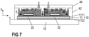
Figures 4 to 7 schematically illustrate subsequent steps of a method for forming a power semiconductor module arrangement according to one example. - In the following detailed description, reference is made to the accompanying drawings. The drawings show specific examples in which the invention may be practiced. It is to be understood that the features and principles described with respect to the various examples may be combined with each other, unless specifically noted otherwise. In the description, as well as in the claims, designations of certain elements as "first element", "second element", "third element" etc. are not to be understood as enumerative. Instead, such designations serve solely to designate different "elements". That is, e.g., the existence of a "third element" does not require the existence of a "first element" and a "second element". An electrical line or electrical connection as described herein may be a single electrically conductive element, or may include at least two individual electrically conductive elements connected in series and/or parallel. Electrical lines and electrical connections may include metal and/or semiconductor material, and may be permanently electrically conductive (i.e., non-switchable). A semiconductor body as described herein may be made from (doped) semiconductor material and may be a semiconductor chip or may be included in a semiconductor chip. A semiconductor body has electrically connecting pads and includes at least one semiconductor element with electrodes.
- Referring to
Figure 1 , a cross-sectional view of an exemplary power semiconductor module is illustrated. The power semiconductor module includes a housing and asubstrate 10. Thesubstrate 10 includes adielectric insulation layer 11, a (structured)first metallization layer 111 attached to thedielectric insulation layer 11, and a second (structured)metallization layer 112 attached to thedielectric insulation layer 11. Thedielectric insulation layer 11 is disposed between the first andsecond metallization layers substrate 10 only comprises afirst metallization layer 111, and that thesecond metallization layer 112 is omitted. - Each of the first and
second metallization layers substrate 10 may be a ceramic substrate, that is, a substrate in which thedielectric insulation layer 11 is a ceramic, e.g., a thin ceramic layer. The ceramic may consist of or include one of the following materials: aluminum oxide; aluminum nitride; zirconium oxide; silicon nitride; boron nitride; or any other dielectric ceramic. For example, thedielectric insulation layer 11 may consist of or include one of the following materials: Al2O3, AlN, SiC, BeO or Si3N4. For instance, thesubstrate 10 may be, e.g., a Direct Copper Bonding (DCB) substrate, a Direct Aluminum Bonding (DAB) substrate, or an Active Metal Brazing (AMB) substrate. Further, thesubstrate 10 may be an Insulated Metal Substrate (IMS). An Insulated Metal Substrate generally comprises adielectric insulation layer 11 comprising (filled) materials such as epoxy resin or polyimide, for example. The material of thedielectric insulation layer 11 may be filled with ceramic particles, for example. Such particles may comprise, e.g., SiO2, Al2O3, AlN, or BN and may have a diameter of between about 1µm and about 50µm. Thesubstrate 10 may also be a conventional printed circuit board (PCB) having a non-ceramicdielectric insulation layer 11. For instance, a non-ceramicdielectric insulation layer 11 may consist of or include a cured resin. - The
substrate 10 is arranged in a housing. In the example illustrated inFigure 1 , thesubstrate 10 is arranged on aground surface 12 of the housing. The housing further comprisessidewalls 42 and alid 44. Thesidewalls 42 and thelid 44 are separate elements. That is, when assembling the power semiconductor module arrangement, thesidewalls 42 may be arranged on the substrate and/or theground surface 12 first, with the lid still being open. Thelid 44 may only be mounted on thesidewalls 42 at a later stage during the assembly. In some examples, theground surface 12 of the housing may be omitted. In such cases thesubstrate 10 itself may form the ground surface of the housing. Thesubstrate 10 may also be arranged on a base plate orheat sink 12, for example. In the example inFigure 1 , only onesubstrate 10 is arranged on the ground surface, base plate or heat sink 12 (only referred to as ground surface in the following). In some power semiconductor module arrangements, more than onesubstrate 10 may be arranged in a single housing. Theground surface 12, thesidewalls 42 and thelid 44 may include a metal or a metal alloy, for example. It is, however, also possible that theground surface 12,sidewalls 42 andlid 44 comprise an electrically insulating material such as a plastic or ceramic material, for example. The housing may also include a liquid crystal polymer, for example. Other materials are also possible. In the examples illustrated herein, the housing is rectangular or has a square shape and has foursidewalls 42. This, however, is only an example. It is generally possible that the housing comprises any number of sidewalls (e.g., three, four, or even more). The number of sidewalls is not relevant for the present invention. - The
substrate 10 may be connected to theground surface 12 by means of a connection layer (not specifically illustrated inFigure 1 ). Such a connection layer may be a solder layer, a layer of an adhesive material, or a layer of a sintered metal powder, e.g., a sintered silver powder, for example. Any other kind of electrically conducting or non-conducting connection layer is also possible. - One or
more semiconductor bodies 20 may be arranged on thesubstrate 10. Each of thesemiconductor bodies 20 arranged on thesubstrate 10 may include a diode, an IGBT (Insulated-Gate Bipolar Transistor), a MOSFET (Metal-Oxide-Semiconductor Field-Effect Transistor), a JFET (Junction Field-Effect Transistor), a HEMT (High-Electron-Mobility Transistor), or any other suitable controllable semiconductor element. - The one or
more semiconductor bodies 20 may form a semiconductor arrangement on thesubstrate 10. InFigure 1 , only twosemiconductor bodies 20 are exemplarily illustrated. Thesecond metallization layer 112 of thesubstrate 10 inFigure 1 is a continuous layer. Thefirst metallization layer 111 of the example inFigure 1 is also a continuous layer. However, thefirst metallization layer 111, or thesecond metallization layer 112, or both can also be structured layers. "Structured layer" means that, e.g., therespective metallization layer Different semiconductor bodies 20 may be mounted to the same or to different sections of thefirst metallization layer 111. Different sections of thefirst metallization layer 111 may have no electrical connection or may be electrically connected to one or more other sections using, e.g., bonding wires. Electrical connections may also include bonding ribbons, connection plates or conductor rails, for example, to name just a few examples. According to another example, thesecond metallization layer 112 can be omitted altogether. The one ormore semiconductor bodies 20 may be electrically and mechanically connected to thesubstrate 10 by an electricallyconductive connection layer 22. Such an electricallyconductive connection layer 22 may be a solder layer, a layer of an electrically conductive adhesive, or a layer of a sintered metal powder, e.g., a sintered silver powder, for example. - The power semiconductor module may further include
terminal elements 30. Theterminal elements 30 are electrically connected to thesubstrate 10, e.g., to thefirst metallization layer 111 of thesubstrate 10, and form a contact element which provides an electrical connection between the inside and the outside of the housing. Theterminal elements 30 may extend through the housing as shown inFigures 1 and 2 , or they may be formed as part of the housing, and connected electrically to thesubstrate 10 via further conductors without being in direct physical contact with thesubstrate 10. A first end of theterminal elements 30 may be electrically and mechanically connected to thefirst metallization layer 111 by an electrically conductive connection layer (not specifically illustrated). Such an electrically conductive connection layer may be a solder layer, a layer of an electrically conductive adhesive, or a layer of a sintered metal powder, e.g., a sintered silver powder, for example. A second end of theterminal elements 30 protrudes out of the housing to allow theterminal element 30 to be electrically contacted from the outside. Thelid 44 may comprise through holes or openings through which theterminal elements 30 may protrude such that their first end is inside the housing and their second end is outside the housing. Theterminal elements 30 may protrude vertically (i.e., perpendicular to a top surface of the substrate 10) out of the housing when the housing is arranged to surround thesubstrate 10. According to another example,terminal elements 30 may also protrude horizontally (parallel to the top surface of the substrate 10) through asidewall 42 of the housing. - The semiconductor module arrangement illustrated in
Figure 1 further comprises press-on pins 48. The press-onpins 48 are attached to thelid 44 and extend vertically from thelid 44 towards thesubstrate 10. The press-onpins 48 contact thesubstrate 10, for example. InFigure 1 , the press-onpins 48 are illustrated as being arranged at a certain distance from thedifferent semiconductor bodies 20 in a horizontal direction x. This, however, is only an example. Generally, press-onpins 48 may also be arranged in close vicinity to at least one of thesemiconductor bodies 20. According to another example, press-onpins 48 may contact asemiconductor body 20 instead of on thesubstrate 10. If the press-onpin 48 contacts asemiconductor body 20, therespective semiconductor body 20 is arranged between the press-onpin 48 and thesubstrate 10. The press-onpin 48 may be arranged at a central position within the housing. That is, the press-onpin 48 may be arranged at a first distance from a first sidewall and at a second distance from a second sidewall opposite the first sidewall, wherein the first distance equals the second distance, and at a third distance from a third sidewall and at a fourth distance from a fourth sidewall opposite the third sidewall, wherein the third distance equals the fourth distance. Press-on pins, however, may also be arranged at any other suitable position within the housing. - When the semiconductor module arrangement is fully assembled, the
substrate 10 is pressed onto theground surface 12 of the housing by means of the press-onpins 48 in order to reduce a thermal resistance between thesubstrate 10 and theground surface 12. Further, thesubstrate 10 is thereby kept in a desired position and is prevented from shifting inside the housing. When thelid 44 is arranged on thesidewalls 42 to close the housing, the press-onpins 48 contact thesubstrate 10 or one of thesemiconductor bodies 20 and exert a pressure on the press-on pins 48. The bold arrows inFigure 1 illustrate a direction in which thelid 44 is moved while closing the housing and a direction of the pressure exerted on the press-onpin 48 once the housing is fully closed. - In the example illustrated in
Figure 1 , the power semiconductor module arrangement comprises a plurality ofterminal elements 30 and a plurality of press-on pins 48. This, however, is only an example. Generally, a power semiconductor module arrangement may comprise at least one functional element, the at least one functional element comprising at least one terminal element and/or at least one press-onpin 48. The term "functional element" as used herein refers to any element extending from thelid 44 of the housing in a vertical direction towards thesubstrate 10 that exhibits at least one specific function within the power semiconductor module arrangement. The terminal elements, for example, fall under the term functional element as they are configured to conduct currents / voltages and to transmit signals between the inside and the outside of the housing. The press-onpins 48 are used to press thesubstrate 10 towards theground surface 12, and are therefore functional elements. There may be, however, any other kinds of functional elements that exhibit other functions and that extend from thelid 44 towards thesubstrate 10. Such functional elements do not necessarily extend all the way towards the substrate. It is generally also possible that a functional element does not directly contact thesubstrate 10 or any of the elements mounted thereon. - Many power semiconductor modules further include a casting
compound 5, as is illustrated in the example ofFigure 2 . The castingcompound 5 may consist of or include a silicone gel or may be a rigid molding compound, for example. The castingcompound 5 may partly fill the interior of the housing, thereby covering thesubstrate 10 and thesemiconductor bodies 20, and any other components andelectrical connections 24 that are arranged on thesubstrate 10.Electrical connections 24 such as, e.g., bonding wires or bonding ribbons, may electrically couple thesemiconductor bodies 20 to thefirst metallization layer 111, toother semiconductor bodies 20, or to any other components that may be arranged inside the housing. Theterminal elements 30 may be partly embedded in the castingcompound 5. At least the second ends of theterminal elements 30, however, may not be covered by the castingcompound 5 and may protrude from the castingcompound 5. The same applies for the press-on pins 48. The castingcompound 5 is configured to protect the components and electrical connections inside the power semiconductor module arrangement, in particular inside the housing, from certain environmental conditions, mechanical damage and insulation faults. - When the casting
compound 5 is formed, usually a liquid, semi-liquid or viscous material is poured into the housing, thereby forming a liquid, semi-liquid or viscous pre-layer. Generally, it is possible that thelid 44 is already arranged on thesidewalls 42 at this point. Thelid 44, for example, may comprise an opening through which the liquid, semi-liquid or viscous material may be poured into the housing. A heating step may follow during which liquid that is present in the pre-layer is at least partly evaporated. In this way, the pre-layer is hardened to form the resultingcasting compound 5. The liquid, semi-liquid or viscous material is generally poured into the housing at room temperature. During the following heating step, the liquid, semi-liquid or viscous material is heated to temperatures of up to 120°C or even more. For example, the liquid, semi-liquid or viscous material of the pre-layer may be heated to temperatures of between 60°C and 120°C. When heat is applied to the liquid, semi-liquid or viscous material of the castingcompound 5, liquid that is present in the pre-layer evaporates and a cross-linking process is started. After a certain time, e.g., 10 to 20 minutes, the material is sufficiently cured, thereby forming the resultingcasting compound 5. - During the heating step, the liquid, semi-liquid or viscous material expands to a certain degree, due to the high temperatures. As has been described above, certain functional elements such as, e.g., the
terminal elements 30 or the press-onpins 48, extend from thelid 44 of the housing toward thesubstrate 10. A part of such functional elements, therefore, is embedded in the liquid, semi-liquid or viscous material of the pre-layer, while another part of the functional elements extends out of the liquid, semi-liquid or viscous material and further towards thelid 44. This may be the case for other functional elements of the power semiconductor module as well. There is a risk, however, that when the material expands during the heating step, and further under the influence of, e.g., a capillary or any other effects, the material creeps along such functional elements in a vertical direction y to the inner surface of thelid 44, the inner surface of thelid 44 being a surface facing towards thesubstrate 10. In this way, the inner surface of thelid 44 may be wetted by the material of the pre-layer. If a certain amount of material collects on the inner surface of thelid 44, it may further creep along thelid 44 towards thesidewalls 42. There it may unintentionally leak out of the housing, especially at the beginning of the heating step when the material is not yet sufficiently cross-linked and hardened. The leaking of material out of the housing is schematically illustrated in the arrangement illustrated inFigure 3 . The material wetting thelid 44 and leaking out of the housing may negatively affect the performance and the lifetime of the power semiconductor module. - In order to prevent the material of the pre-layer that is supposed to form the casting
compound 5 from wetting the inside of thelid 44 and from leaking out of the housing, instead of mounting thelid 44 on thesidewalls 42 before filling the liquid, semi-liquid or viscous material of the pre-layer into the housing, the liquid, semi-liquid or viscous material of the pre-layer is filled into the housing first, and only then thelid 44 is arranged on thesidewalls 42. Thelid 44, however, is arranged on thesidewalls 42 before hardening the liquid, semi-liquid or viscous material of the pre-layer. The functional elements, therefore, are immersed into the liquid, semi-liquid or viscous material of the pre-layer while mounting thelid 44 on thesidewalls 42. The functional elements displace the liquid, semi-liquid or viscous material of the pre-layer to a certain degree. That is, after mounting thelid 44 on the sidewalls, a height of the liquid, semi-liquid or viscous material of the pre-layer in the vertical direction y above thesubstrate 10 increases to a certain degree. The increase in height may be marginal, if there are only few functional elements and/or only small functional elements of comparably small volume. The increase in height may be somewhat more if there are many functional elements and/or large functional elements of a larger volume. - When the
lid 44 is arranged on thesidewalls 42 after filling the liquid, semi-liquid or viscous material of the pre-layer into the housing, the effect of material creeping along the functional elements toward the inner surface of thelid 44 and from there leaking out of the housing may be significantly reduced or even completely prevented. The vertical insertion of the functional elements into the liquid, semi-liquid or viscous material of the pre-layer has significant influence on the capillary or any other effects. While the capillary effect or other effects occur in those cases in which the liquid, semi-liquid or viscous material of the pre-layer is filled into the housing after thelid 44 has been arranged on the sidewalls, such effects may be reduced or even entirely avoided by arranging thelid 44 on thesidewalls 42 after filling the liquid, semi-liquid or viscous material of the pre-layer into the housing. - Now referring to
Figures 4 to 7 , an exemplary method is schematically illustrated. As is illustrated inFigure 4 , the substrate 10 (withsemiconductor bodies 20 and other elements and components mounted thereon) is arranged on aground surface 12. Thesidewalls 42 are arranged to surround thesubstrate 10. In a following step, which is schematically illustrated inFigure 5 , the liquid, semi-liquid or viscous material of the pre-layer is filled into the housing (i.e. into the cavity formed by the sidewalls 42) to cover thesubstrate 10 and the components mounted thereon. The liquid, semi-liquid or viscous material of the pre-layer, however, does not completely fill the cavity formed by thesidewalls 42. At least part of the cavity remains free from the liquid, semi-liquid or viscous material of the pre-layer. - Now referring to
Figure 6 , thelid 44 with the functional elements attached thereto is mounted on thesidewalls 42. A volume that is not filled with the liquid, semi-liquid or viscous material of the pre-layer remains between the liquid, semi-liquid or viscous material of the pre-layer and the inner surface of thelid 44. That is, the inner surface of thelid 44 is not in direct contact with the liquid, semi-liquid or viscous material of the pre-layer. In a subsequent step, which is schematically illustrated inFigure 7 , the liquid, semi-liquid or viscous material of the pre-layer is hardened/cured, thereby forming thefinal casting compound 5. - The method described with respect to
Figures 4 to 7 has several further advantages. For example, the entire opening formed by thesidewalls 42 remains available during the step of filling the liquid, semi-liquid or viscous material of the pre-layer into the housing. That is, a position of a nozzle through which the liquid, semi-liquid or viscous material is injected into the housing may be freely chosen and is not restricted by a comparably small opening provided in thelid 44. It is even possible to use a plurality of nozzles at different positions. In this way, the liquid, semi-liquid or viscous material may be filled into the housing in a shorter time which results in decreased costs.
Claims (7)
- A method comprising:pouring a liquid, semi-liquid or viscous material into a cavity formed by sidewalls (42) of a housing, thereby covering a substrate (10) that is arranged in the cavity formed by the sidewalls (42);arranging a lid (44) on the sidewalls (42), thereby covering the cavity formed by the sidewalls (42), wherein the lid (44) comprises at least one functional element that extends from the lid (44) into the liquid, semi-liquid or viscous material in a direction towards the substrate (10) once the lid (44) is in its final mounting position; andcuring the liquid, semi-liquid or viscous material in order to form a casting compound (5).
- The method of claim 1, wherein the step of curing the liquid, semi-liquid or viscous material comprises heating the liquid, semi-liquid or viscous material to a temperature of between 60°C and 120°C.
- The method of claim 2, wherein the liquid, semi-liquid or viscous material is heated to a temperature of between 60°C and 120°C for between 10 and 20 minutes.
- The method of any of claims 1 to 3, wherein, when pouring the liquid, semi-liquid or viscous material into the cavity formed by the sidewalls (42), the cavity formed by the sidewalls (42) is only partly filled with the liquid, semi-liquid or viscous material such that, after arranging the lid (44) on the sidewalls (42), a cavity remains between the liquid, semi-liquid or viscous material and the lid (44).
- The method of any of claims 1 to 4, wherein, the at least one functional element displaces the liquid, semi-liquid or viscous material of the pre-layer during the step of arranging the lid (44) on the sidewalls (42).
- The method of any of claims 1 to 5, wherein the step of pouring a liquid, semi-liquid or viscous material into a cavity formed by sidewalls (42) of a housing comprises pouring a silicone gel into the cavity.
- The method of any of the preceding claims, further comprising mounting at least one semiconductor body (20) on the substrate (10) before pouring the liquid, semi-liquid or viscous material into the cavity formed by the sidewalls.
Priority Applications (3)
| Application Number | Priority Date | Filing Date | Title |
|---|---|---|---|
| EP22172217.6A EP4276888A1 (en) | 2022-05-09 | 2022-05-09 | Method for producing a power semiconductor module |
| US18/141,634 US20230360982A1 (en) | 2022-05-09 | 2023-05-01 | Method for producing a power semiconductor module |
| CN202310492292.4A CN117038476A (en) | 2022-05-09 | 2023-05-04 | Method for manufacturing power semiconductor modules |
Applications Claiming Priority (1)
| Application Number | Priority Date | Filing Date | Title |
|---|---|---|---|
| EP22172217.6A EP4276888A1 (en) | 2022-05-09 | 2022-05-09 | Method for producing a power semiconductor module |
Publications (1)
| Publication Number | Publication Date |
|---|---|
| EP4276888A1 true EP4276888A1 (en) | 2023-11-15 |
Family
ID=81595613
Family Applications (1)
| Application Number | Title | Priority Date | Filing Date |
|---|---|---|---|
| EP22172217.6A Pending EP4276888A1 (en) | 2022-05-09 | 2022-05-09 | Method for producing a power semiconductor module |
Country Status (3)
| Country | Link |
|---|---|
| US (1) | US20230360982A1 (en) |
| EP (1) | EP4276888A1 (en) |
| CN (1) | CN117038476A (en) |
Citations (3)
| Publication number | Priority date | Publication date | Assignee | Title |
|---|---|---|---|---|
| US20190164880A1 (en) * | 2017-11-29 | 2019-05-30 | Mitsubishi Electric Corporation | Semiconductor module, method for manufacturing the same and power conversion apparatus |
| US20200243411A1 (en) * | 2017-05-10 | 2020-07-30 | Mitsubishi Electric Corporation | Semiconductor device and method of manufacturing semiconductor device, power conversion device, and moving body |
| US20220108939A1 (en) * | 2020-10-07 | 2022-04-07 | Stmicroelectronics S.R.L. | Blocking element for connecting pins of semiconductor dice |
Family Cites Families (4)
| Publication number | Priority date | Publication date | Assignee | Title |
|---|---|---|---|---|
| DE112014005694B4 (en) * | 2014-01-27 | 2020-07-30 | Hitachi, Ltd. | Semiconductor module |
| US9548255B1 (en) * | 2015-08-17 | 2017-01-17 | Freescale Semiconductor, Inc. | IC package having non-horizontal die pad and flexible substrate therefor |
| DE202018100486U1 (en) * | 2018-01-30 | 2018-02-22 | Infineon Technologies Ag | The power semiconductor module |
| US12009352B2 (en) * | 2019-09-26 | 2024-06-11 | Illumina, Inc. | Fabricating wafers with electrical contacts on a surface parallel to an active surface |
-
2022
- 2022-05-09 EP EP22172217.6A patent/EP4276888A1/en active Pending
-
2023
- 2023-05-01 US US18/141,634 patent/US20230360982A1/en active Pending
- 2023-05-04 CN CN202310492292.4A patent/CN117038476A/en active Pending
Patent Citations (3)
| Publication number | Priority date | Publication date | Assignee | Title |
|---|---|---|---|---|
| US20200243411A1 (en) * | 2017-05-10 | 2020-07-30 | Mitsubishi Electric Corporation | Semiconductor device and method of manufacturing semiconductor device, power conversion device, and moving body |
| US20190164880A1 (en) * | 2017-11-29 | 2019-05-30 | Mitsubishi Electric Corporation | Semiconductor module, method for manufacturing the same and power conversion apparatus |
| US20220108939A1 (en) * | 2020-10-07 | 2022-04-07 | Stmicroelectronics S.R.L. | Blocking element for connecting pins of semiconductor dice |
Also Published As
| Publication number | Publication date |
|---|---|
| CN117038476A (en) | 2023-11-10 |
| US20230360982A1 (en) | 2023-11-09 |
Similar Documents
| Publication | Publication Date | Title |
|---|---|---|
| US11978700B2 (en) | Power semiconductor module arrangement | |
| US12500152B2 (en) | Power semiconductor module, method for assembling a power semiconductor module and housing for a power semiconductor module | |
| EP3929973B1 (en) | A power semiconductor module and a method for producing a power semiconductor module | |
| US11581230B2 (en) | Power semiconductor module and a method for producing a power semiconductor module | |
| US12564094B2 (en) | Power semiconductor module arrangement and method for producing the same | |
| US6921969B2 (en) | Semiconductor module and method of producing a semiconductor module | |
| EP3736855A1 (en) | Power semiconductor module arrangement and method for producing the same | |
| EP3477694B1 (en) | Power semiconductor module with partially coated power terminals | |
| EP4270469A1 (en) | Power semiconductor module | |
| US20230360982A1 (en) | Method for producing a power semiconductor module | |
| US12261063B2 (en) | Method and device for producing a housing | |
| US12456654B2 (en) | Power semiconductor modules | |
| US12482725B2 (en) | Power semiconductor module arrangements and methods for producing power semiconductor module arrangements | |
| US20260090385A1 (en) | Semiconductor module comprising a housing | |
| EP4604176A1 (en) | Semiconductor module arrangement, electronics carrier for a semiconductor module arrangement, and method for producing a semiconductor module arrangement | |
| US20250273520A1 (en) | Housing, semiconductor module having a housing, and method for assembling a semiconductor module | |
| JP2025171218A (en) | Power semiconductor device and method for manufacturing the same |
Legal Events
| Date | Code | Title | Description |
|---|---|---|---|
| PUAI | Public reference made under article 153(3) epc to a published international application that has entered the european phase |
Free format text: ORIGINAL CODE: 0009012 |
|
| STAA | Information on the status of an ep patent application or granted ep patent |
Free format text: STATUS: REQUEST FOR EXAMINATION WAS MADE |
|
| 17P | Request for examination filed |
Effective date: 20230411 |
|
| AK | Designated contracting states |
Kind code of ref document: A1 Designated state(s): AL AT BE BG CH CY CZ DE DK EE ES FI FR GB GR HR HU IE IS IT LI LT LU LV MC MK MT NL NO PL PT RO RS SE SI SK SM TR |