EP4276500A1 - Imaging lens assembly and electronic device - Google Patents
Imaging lens assembly and electronic device Download PDFInfo
- Publication number
- EP4276500A1 EP4276500A1 EP23166472.3A EP23166472A EP4276500A1 EP 4276500 A1 EP4276500 A1 EP 4276500A1 EP 23166472 A EP23166472 A EP 23166472A EP 4276500 A1 EP4276500 A1 EP 4276500A1
- Authority
- EP
- European Patent Office
- Prior art keywords
- light blocking
- structures
- central aperture
- radius
- imaging lens
- Prior art date
- Legal status (The legal status is an assumption and is not a legal conclusion. Google has not performed a legal analysis and makes no representation as to the accuracy of the status listed.)
- Granted
Links
Images










Classifications
-
- G—PHYSICS
- G02—OPTICS
- G02B—OPTICAL ELEMENTS, SYSTEMS OR APPARATUS
- G02B7/00—Mountings, adjusting means, or light-tight connections, for optical elements
- G02B7/02—Mountings, adjusting means, or light-tight connections, for optical elements for lenses
-
- G—PHYSICS
- G02—OPTICS
- G02B—OPTICAL ELEMENTS, SYSTEMS OR APPARATUS
- G02B7/00—Mountings, adjusting means, or light-tight connections, for optical elements
-
- G—PHYSICS
- G02—OPTICS
- G02B—OPTICAL ELEMENTS, SYSTEMS OR APPARATUS
- G02B7/00—Mountings, adjusting means, or light-tight connections, for optical elements
- G02B7/02—Mountings, adjusting means, or light-tight connections, for optical elements for lenses
- G02B7/021—Mountings, adjusting means, or light-tight connections, for optical elements for lenses for more than one lens
-
- G—PHYSICS
- G02—OPTICS
- G02B—OPTICAL ELEMENTS, SYSTEMS OR APPARATUS
- G02B5/00—Optical elements other than lenses
- G02B5/005—Diaphragms
-
- G—PHYSICS
- G02—OPTICS
- G02B—OPTICAL ELEMENTS, SYSTEMS OR APPARATUS
- G02B27/00—Optical systems or apparatus not provided for by any of the groups G02B1/00 - G02B26/00, G02B30/00
- G02B27/0018—Optical systems or apparatus not provided for by any of the groups G02B1/00 - G02B26/00, G02B30/00 with means for preventing ghost images
-
- G—PHYSICS
- G02—OPTICS
- G02B—OPTICAL ELEMENTS, SYSTEMS OR APPARATUS
- G02B3/00—Simple or compound lenses
-
- G—PHYSICS
- G03—PHOTOGRAPHY; CINEMATOGRAPHY; ANALOGOUS TECHNIQUES USING WAVES OTHER THAN OPTICAL WAVES; ELECTROGRAPHY; HOLOGRAPHY
- G03B—APPARATUS OR ARRANGEMENTS FOR TAKING PHOTOGRAPHS OR FOR PROJECTING OR VIEWING THEM; APPARATUS OR ARRANGEMENTS EMPLOYING ANALOGOUS TECHNIQUES USING WAVES OTHER THAN OPTICAL WAVES; ACCESSORIES THEREFOR
- G03B9/00—Exposure-making shutters; Diaphragms
- G03B9/02—Diaphragms
-
- G—PHYSICS
- G03—PHOTOGRAPHY; CINEMATOGRAPHY; ANALOGOUS TECHNIQUES USING WAVES OTHER THAN OPTICAL WAVES; ELECTROGRAPHY; HOLOGRAPHY
- G03B—APPARATUS OR ARRANGEMENTS FOR TAKING PHOTOGRAPHS OR FOR PROJECTING OR VIEWING THEM; APPARATUS OR ARRANGEMENTS EMPLOYING ANALOGOUS TECHNIQUES USING WAVES OTHER THAN OPTICAL WAVES; ACCESSORIES THEREFOR
- G03B30/00—Camera modules comprising integrated lens units and imaging units, specially adapted for being embedded in other devices, e.g. mobile phones or vehicles
-
- G—PHYSICS
- G03—PHOTOGRAPHY; CINEMATOGRAPHY; ANALOGOUS TECHNIQUES USING WAVES OTHER THAN OPTICAL WAVES; ELECTROGRAPHY; HOLOGRAPHY
- G03B—APPARATUS OR ARRANGEMENTS FOR TAKING PHOTOGRAPHS OR FOR PROJECTING OR VIEWING THEM; APPARATUS OR ARRANGEMENTS EMPLOYING ANALOGOUS TECHNIQUES USING WAVES OTHER THAN OPTICAL WAVES; ACCESSORIES THEREFOR
- G03B9/00—Exposure-making shutters; Diaphragms
- G03B9/08—Shutters
Definitions
- the present disclosure relates to an imaging lens assembly and an electronic device. More particularly, the present disclosure relates to an imaging lens assembly which can be applied to portable electronic devices.
- an imaging lens assembly includes a plurality of optical lens elements, a single-piece-formed light blocking sheet and a lens barrel.
- the single-piece-formed light blocking sheet corresponds to the plurality of optical lens elements.
- the lens barrel has a circular light-passing hole corresponding to the plurality of optical lens elements and the single-piece-formed light blocking sheet.
- the single-piece-formed light blocking sheet has a central aperture corresponding to the lens barrel and the plurality of optical lens elements, and a maximum aperture diameter is defined by the central aperture.
- the single-piece-formed light blocking sheet includes a plurality of light blocking structures surrounding and disposed adjacent to the central aperture, and a number of the plurality of light blocking structures is three to ten.
- a center of each of the light blocking structures is closer to a center of the central aperture than two ends of each of the light blocking structures, and the two ends of each of the light blocking structures extend toward the maximum aperture diameter of the central aperture.
- a maximum aperture radius of the central aperture is Rmax
- a minimum inner radius of the central aperture is defined near the center of each of the light blocking structures, the minimum inner radius is Rmin
- a roundness coefficient of the central aperture is tc
- the single-piece-formed light blocking sheet can further include a plurality of radius structures.
- the plurality of radius structures can surround and be disposed adjacent to the central aperture, and a number of the plurality of radius structures can be three to ten.
- Each of the radius structures can be connected to two of the light blocking structures adjacent thereto, and each of the radius structures can be arc-shaped.
- the plurality of radius structures and the plurality of light blocking structures can be disposed alternately and surround the central aperture.
- the single-piece-formed light blocking sheet can further include a plurality of radius structures
- the plurality of radius structures can surround and be disposed adjacent to the central aperture
- each of the radius structures can be connected to two of the light blocking structures adjacent thereto
- each of the light blocking structures can be a straight-line segment
- each of the radius structures can be arc-shaped.
- the imaging lens assembly of the foregoing aspect wherein when the roundness coefficient of the central aperture is tc, the following condition can be satisfied: 0.83% ⁇ tc ⁇ 8.6%.
- the imaging lens assembly of the foregoing aspect wherein when the roundness coefficient of the central aperture is tc, the following condition can be satisfied: 0.83% ⁇ tc ⁇ 6.8%.
- the imaging lens assembly of the foregoing aspect wherein when the roundness coefficient of the central aperture is tc, the following condition can be satisfied: 0.68% ⁇ tc ⁇ 4.1%.
- the number of the plurality of light blocking structures can be five to nine.
- the imaging lens assembly of the foregoing aspect wherein when a thickness of the single-piece-formed light blocking sheet is S, the following condition can be satisfied: 5 ⁇ m ⁇ S ⁇ 210 ⁇ m.
- an electronic device includes the imaging lens assembly according to the aforementioned aspect and an image sensor disposed on an image surface of the imaging lens assembly.
- the present disclosure provides an imaging lens assembly including a plurality of optical lens elements, a single-piece-formed light blocking sheet and a lens barrel.
- the single-piece-formed light blocking sheet corresponds to the optical lens elements.
- the lens barrel has a circular light-passing hole corresponding to the optical lens elements and the single-piece-formed light blocking sheet.
- the single-piece-formed light blocking sheet has a central aperture corresponding to the lens barrel and the optical lens elements, and a maximum aperture diameter is defined by the central aperture.
- the single-piece-formed light blocking sheet includes a plurality of light blocking structures surrounding and disposed adjacent to the central aperture, and a number of the plurality of light blocking structures is three to ten.
- a center of each of the light blocking structures is closer to a center of the central aperture than two ends of each of the light blocking structures, and the two ends of each of the light blocking structures extend toward the maximum aperture diameter of the central aperture.
- a maximum aperture radius of the central aperture is Rmax
- a minimum inner radius of the central aperture is defined near the center of each of the light blocking structures, the minimum inner radius is Rmin
- a roundness coefficient of the central aperture is tc
- the single-piece-formed light blocking sheet can be an aperture stop of the imaging lens assembly, the maximum aperture diameter of the central aperture is equal to an entrance pupil diameter (EPD) of the imaging lens assembly.
- the single-piece-formed light blocking sheet can have effects similar to that of the multi-blade aperture stop of a single-lens reflex camera, so that the imaging performance of the physical light source can be effectively controlled by the light blocking structures so as to make the light source identifiable, and the size of the central aperture can be precisely controlled to achieve an ideal imaging effect.
- the single-piece-formed light blocking sheet can further include a plurality of radius structures, and the plurality of radius structures surround and are disposed adjacent to the central aperture.
- a number of the plurality of radius structures can be three to ten, each of the radius structures is connected to two of the light blocking structures adjacent thereto, and each of the radius structures can be arc-shaped. Therefore, the arc-shaped arrangement can prevent excessive light blocking and from affecting the specifications of the imaging lens assembly.
- the plurality of radius structures and the plurality of light blocking structures are disposed alternately and surround the central aperture. Therefore, by the arrangement that the central aperture includes the radius structures, it is favorable for preventing the excessive length of the light blocking structures.
- Each of the light blocking structures is a straight-line segment, and each of the radius structures is arc-shaped. Therefore, the concentrated light beam of the strong light source will be reflected by the straight-line light blocking structures at the same time, and the arrangement of the arc-shaped radius structures can prevent excessive light blocking of the strong light source by the straight-line segment, so that the imaging light of the strong light source can pass through completely.
- the roundness coefficient of the central aperture is tc
- the following condition is satisfied: 0.83% ⁇ tc ⁇ 8.6%. Therefore, it is favorable for preventing excessive light blocking, so that the low-light photography will not be affected. Furthermore, the following condition can be satisfied: 0.83% ⁇ tc ⁇ 6.8%. Therefore, it is favorable for preventing the imaging light of the weak light source from being affected, and it has better performance when shooting objects with the weak light source. Furthermore, the following condition can be satisfied: 0.68% ⁇ tc ⁇ 4.1%. Therefore, the amount of incoming light can be increased to ensure better imaging performance for shooting in the night environment.
- the number of the plurality of light blocking structures can be five to nine. Therefore, an appropriate number of the light blocking structures are conducive to maintaining a balance between a high amount of incident light and high quality.
- a thickness of the single-piece-formed light blocking sheet is S
- the following condition is satisfied: 5 ⁇ m ⁇ S ⁇ 210 ⁇ m. Therefore, within the specific thickness range, it is not easy to generate additional non-ideal light under the premise of a strict real-shot situation.
- the present disclosure provides an electronic device.
- the electronic device includes the imaging lens assembly according to the aforementioned aspect and an image sensor disposed on an image surface of the imaging lens assembly.
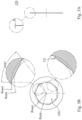
- Fig. 1A is a schematic view of an imaging lens assembly 100 according to the 1st embodiment of the present disclosure.
- Fig. 1B is an exploded view of the imaging lens assembly 100 of Fig. 1A .
- the imaging lens assembly 100 includes a plurality of optical lens elements (reference number is omitted), a single-piece-formed light blocking sheet 120, and a lens barrel 101.
- the plurality of optical lens elements and the single-piece-formed light blocking sheet 120 are accommodated in the lens barrel 101.
- the lens barrel 101 has a circular light-passing hole 110 corresponding to the optical lens elements and the single-piece-formed light blocking sheet 120.
- the single-piece-formed light blocking sheet 120 corresponds to the optical lens elements, and an image surface 102 is located on the most image side of the lens barrel 101.
- a number of the optical lens elements is five, and the five optical lens elements are, in order from an object side to an image side of the imaging lens assembly 100, a first optical lens element 131, a second optical lens element 132, a third optical lens element 133, a fourth optical lens element 134, and a fifth optical lens element 135.
- the single-piece-formed light blocking sheet 120 is a light blocking sheet disposed between the lens barrel 101 and the first optical lens element 131 in the imaging lens assembly 100.
- the imaging lens assembly 100 of the present disclosure can further include other optical elements, such as light blocking sheets, spacers, retainers, etc.
- 1A can further include three light blocking sheets 141, 142, 144, a spacer 143, and a retainer 145. It should be noted that the position of the single-piece-formed light blocking sheet and the arrangement of the light blocking sheet, the spacer and the retainer can be adjusted corresponding to the actual needs, and the present disclosure is not limited thereto.
- Fig. 2A is a cross-sectional view of a single-piece-formed light blocking sheet 120 of the imaging lens assembly 100 according to the 1st example of the 1st embodiment of Fig. 1A .
- Fig. 2B is a schematic view of the single-piece-formed light blocking sheet 120 of Fig. 2A .
- the single-piece-formed light blocking sheet 120 has a central aperture 1201 corresponding to the lens barrel 101 and the optical lens elements.
- a maximum aperture diameter is defined by the central aperture 1201, and a minimum inner radius of the central aperture 1201 is defined near a center of each of a plurality of light blocking structures 121.
- the single-piece-formed light blocking sheet 120 includes the plurality of light blocking structures 121 surrounding and disposed adjacent to the central aperture 1201.
- the center of each of the light blocking structures 121 is closer to a center of the central aperture 1201 than two ends of each of the light blocking structures 121, and the two ends of each of the light blocking structures 121 extend toward the maximum aperture diameter of the central aperture 1201.
- a number of the light blocking structures 121 is nine, and when an angle between the connecting lines from the center of the central aperture 1201 to the two ends of each of the light blocking structures 121 is Ang1, Ang1 is 40 degrees, but the present disclosure is not limited thereto.
- Fig. 3A is a cross-sectional view of a single-piece-formed light blocking sheet 120 of the imaging lens assembly 100 according to the 2nd example of the 1st embodiment of Fig. 1A .
- Fig. 3B is a schematic view of the single-piece-formed light blocking sheet 120 of Fig. 3A .
- the single-piece-formed light blocking sheet 120 has a central aperture 1201 corresponding to the lens barrel 101 and the optical lens elements.
- a maximum aperture diameter is defined by the central aperture 1201, and a minimum inner radius of the central aperture 1201 is defined near a center of each of a plurality of light blocking structures 121.
- the single-piece-formed light blocking sheet 120 includes the plurality of light blocking structures 121 surrounding and disposed adjacent to the central aperture 1201.
- the center of each of the light blocking structures 121 is closer to a center of the central aperture 1201 than two ends of each of the light blocking structures 121, and the two ends of each of the light blocking structures 121 extend toward the maximum aperture diameter of the central aperture 1201.
- a number of the light blocking structures 121 is seven, and when an angle between the connecting lines from the center of the central aperture 1201 to the two ends of each of the light blocking structures 121 is Ang1, Ang1 is 51.429 degrees, but the present disclosure is not limited thereto.
- Fig. 4A is a cross-sectional view of a single-piece-formed light blocking sheet 120 of the imaging lens assembly 100 according to the 3rd example of the 1st embodiment of Fig. 1A .
- Fig. 4B is a schematic view of the single-piece-formed light blocking sheet 120 of Fig. 4A .
- the single-piece-formed light blocking sheet 120 has a central aperture 1201 corresponding to the lens barrel 101 and the optical lens elements.
- a maximum aperture diameter is defined by the central aperture 1201, and a minimum inner radius of the central aperture 1201 is defined near a center of each of a plurality of light blocking structures 121.
- the single-piece-formed light blocking sheet 120 includes the plurality of light blocking structures 121 and a plurality of radius structures 122.
- the light blocking structures 121 and the radius structures 122 surround and are disposed adjacent to the central aperture 1201, and the light blocking structures 121 and the radius structures 122 are disposed alternately and surround the central aperture 1201.
- the center of each of the light blocking structures 121 is closer to a center of the central aperture 1201 than two ends of each of the light blocking structures 121, the two ends of each of the light blocking structures 121 extend toward the maximum aperture diameter of the central aperture 1201, and each of the radius structures 122 is connected to two of the light blocking structures 121 adjacent thereto.
- a number of the light blocking structures 121 is seven, and each of the light blocking structures 121 is a straight-line segment.
- a number of the radius structures 122 is seven, and each of the radius structures 122 is arc-shaped.
- Fig. 5A is a cross-sectional view of a single-piece-formed light blocking sheet 120 of the imaging lens assembly 100 according to the 4th example of the 1st embodiment of Fig. 1A .
- Fig. 5B is a schematic view of the single-piece-formed light blocking sheet 120 of Fig. 5A .
- the single-piece-formed light blocking sheet 120 has a central aperture 1201 corresponding to the lens barrel 101 and the optical lens elements.
- a maximum aperture diameter is defined by the central aperture 1201, and a minimum inner radius of the central aperture 1201 is defined near a center of each of a plurality of light blocking structures 121.
- the single-piece-formed light blocking sheet 120 includes the plurality of light blocking structures 121 and a plurality of radius structures 122.
- the light blocking structures 121 and the radius structures 122 surround and are disposed adjacent to the central aperture 1201, and the light blocking structures 121 and the radius structures 122 are disposed alternately and surround the central aperture 1201.
- the center of each of the light blocking structures 121 is closer to a center of the central aperture 1201 than two ends of each of the light blocking structures 121, the two ends of each of the light blocking structures 121 extend toward the maximum aperture diameter of the central aperture 1201, and each of the radius structures 122 is connected to two of the light blocking structures 121 adjacent thereto.
- a number of the light blocking structures 121 is five, and each of the light blocking structures 121 is a straight-line segment.
- a number of the radius structures 122 is five, and each of the radius structures 122 is arc-shaped.
- Fig. 6A is a cross-sectional view of a single-piece-formed light blocking sheet 120 of the imaging lens assembly 100 according to the 5th example of the 1st embodiment of Fig. 1A .
- Fig. 6B is a schematic view of the single-piece-formed light blocking sheet 120 of Fig. 6A .
- the single-piece-formed light blocking sheet 120 has a central aperture 1201 corresponding to the lens barrel 101 and the optical lens elements.
- a maximum aperture diameter is defined by the central aperture 1201, and a minimum inner radius of the central aperture 1201 is defined near a center of each of a plurality of light blocking structures 121.
- the single-piece-formed light blocking sheet 120 includes the plurality of light blocking structures 121 and a plurality of radius structures 122.
- the light blocking structures 121 and the radius structures 122 surround and are disposed adjacent to the central aperture 1201, and the light blocking structures 121 and the radius structures 122 are disposed alternately and surround the central aperture 1201.
- the center of each of the light blocking structures 121 is closer to a center of the central aperture 1201 than two ends of each of the light blocking structures 121, the two ends of each of the light blocking structures 121 extend toward the maximum aperture diameter of the central aperture 1201, and each of the radius structures 122 is connected to two of the light blocking structures 121 adjacent thereto.
- a number of the light blocking structures 121 is five, and each of the light blocking structures 121 is a straight-line segment.
- a number of the radius structures 122 is five, and each of the radius structures 122 is arc-shaped.
- Fig. 7A is a cross-sectional view of a single-piece-formed light blocking sheet 120 of the imaging lens assembly 100 according to the 6th example of the 1st embodiment of Fig. 1A .
- Fig. 7B is a schematic view of the single-piece-formed light blocking sheet 120 of Fig. 7A .
- the single-piece-formed light blocking sheet 120 has a central aperture 1201 corresponding to the lens barrel 101 and the optical lens elements.
- a maximum aperture diameter is defined by the central aperture 1201, and a minimum inner radius of the central aperture 1201 is defined near a center of each of a plurality of light blocking structures 121.
- the single-piece-formed light blocking sheet 120 includes the plurality of light blocking structures 121 and a plurality of radius structures 122.
- the light blocking structures 121 and the radius structures 122 surround and are disposed adjacent to the central aperture 1201, and the light blocking structures 121 and the radius structures 122 are disposed alternately and surround the central aperture 1201.
- the center of each of the light blocking structures 121 is closer to a center of the central aperture 1201 than two ends of each of the light blocking structures 121, the two ends of each of the light blocking structures 121 extend toward the maximum aperture diameter of the central aperture 1201, and each of the radius structures 122 is connected to two of the light blocking structures 121 adjacent thereto.
- a number of the light blocking structures 121 is four, and each of the light blocking structures 121 is a straight-line segment.
- a number of the radius structures 122 is four, and each of the radius structures 122 is arc-shaped.
- Fig. 8A is a cross-sectional view of a single-piece-formed light blocking sheet 120 of the imaging lens assembly 100 according to the 7th example of the 1st embodiment of Fig. 1A .
- Fig. 8B is a schematic view of the single-piece-formed light blocking sheet 120 of Fig. 8A .
- the single-piece-formed light blocking sheet 120 has a central aperture 1201 corresponding to the lens barrel 101 and the optical lens elements.
- a maximum aperture diameter is defined by the central aperture 1201, and a minimum inner radius of the central aperture 1201 is defined near a center of each of a plurality of light blocking structures 121.
- the single-piece-formed light blocking sheet 120 includes the plurality of light blocking structures 121 and a plurality of radius structures 122.
- the light blocking structures 121 and the radius structures 122 surround and are disposed adjacent to the central aperture 1201, and the light blocking structures 121 and the radius structures 122 are disposed alternately and surround the central aperture 1201.
- the center of each of the light blocking structures 121 is closer to a center of the central aperture 1201 than two ends of each of the light blocking structures 121, the two ends of each of the light blocking structures 121 extend toward the maximum aperture diameter of the central aperture 1201, and each of the radius structures 122 is connected to two of the light blocking structures 121 adjacent thereto.
- a number of the light blocking structures 121 is four, and each of the light blocking structures 121 is a straight-line segment.
- a number of the radius structures 122 is four, and each of the radius structures 122 is arc-shaped.
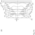
- Fig. 9A is a schematic view of an imaging lens assembly 200 according to the 2nd embodiment of the present disclosure.
- Fig. 9B is an exploded view of the imaging lens assembly 200 of Fig. 9A .
- the imaging lens assembly 200 includes a plurality of optical lens elements (reference number is omitted), a single-piece-formed light blocking sheet 220, and a lens barrel 201.
- the plurality of optical lens elements and the single-piece-formed light blocking sheet 220 are accommodated in the lens barrel 201.
- the lens barrel 201 has a circular light-passing hole 210 corresponding to the optical lens elements and the single-piece-formed light blocking sheet 220.
- the single-piece-formed light blocking sheet 220 corresponds to the optical lens elements, and an image surface 202 is located on the most image side of the lens barrel 201.
- a number of the optical lens elements is seven, and the seven optical lens elements are, in order from an object side to an image side of the imaging lens assembly 200, a first optical lens element 231, a second optical lens element 232, a third optical lens element 233, a fourth optical lens element 234, a fifth optical lens element 235, a sixth optical lens element 236, and a seventh optical lens element 237.
- the single-piece-formed light blocking sheet 220 is a light blocking sheet disposed between the second optical lens element 232 and the third optical lens element 233 in the imaging lens assembly 200.
- the imaging lens assembly 200 of the present disclosure can further include other optical elements, such as light blocking sheets, spacers, retainers, etc.
- the imaging lens assembly 200 can further include five light blocking sheets 241, 242, 243, 244, 246, a spacer 245, and a retainer 247. It should be noted that the position of the single-piece-formed light blocking sheet and the arrangement of the light blocking sheet, the spacer and the retainer can be adjusted corresponding to the actual needs, and the present disclosure is not limited thereto. Furthermore, the imaging lens assembly 200 can further include a filter 203, wherein the filter 203 is disposed between the lens barrel 201 and the image surface 202.
- Fig. 10A is a cross-sectional view of a single-piece-formed light blocking sheet 220 of the imaging lens assembly 200 according to the 1st example of the 2nd embodiment of Fig. 9A .
- Fig. 10B is a schematic view of the single-piece-formed light blocking sheet 220 of Fig. 10A .
- the single-piece-formed light blocking sheet 220 has a central aperture 2201 corresponding to the lens barrel 201 and the optical lens elements.
- a maximum aperture diameter is defined by the central aperture 2201, and a minimum inner radius of the central aperture 2201 is defined near a center of each of a plurality of light blocking structures 221.
- the single-piece-formed light blocking sheet 220 includes the plurality of light blocking structures 221 surrounding and disposed adjacent to the central aperture 2201.
- the center of each of the light blocking structures 221 is closer to a center of the central aperture 2201 than two ends of each of the light blocking structures 221, and the two ends of each of the light blocking structures 221 extend toward the maximum aperture diameter of the central aperture 2201.
- a number of the light blocking structures 221 is nine, and when an angle between the connecting lines from the center of the central aperture 2201 to the two ends of each of the light blocking structures 221 is Ang1, Ang1 is 40 degrees, but the present disclosure is not limited thereto.
- Fig. 11A is a cross-sectional view of a single-piece-formed light blocking sheet 220 of the imaging lens assembly 200 according to the 2nd example of the 2nd embodiment of Fig. 9A .
- Fig. 11B is a schematic view of the single-piece-formed light blocking sheet 220 of Fig. 11A .
- the single-piece-formed light blocking sheet 220 has a central aperture 2201 corresponding to the lens barrel 201 and the optical lens elements.
- a maximum aperture diameter is defined by the central aperture 2201, and a minimum inner radius of the central aperture 2201 is defined near a center of each of a plurality of light blocking structures 221.
- the single-piece-formed light blocking sheet 220 includes the plurality of light blocking structures 221 and a plurality of radius structures 222.
- the light blocking structures 221 and the radius structures 222 surround and are disposed adjacent to the central aperture 2201, and the light blocking structures 221 and the radius structures 222 are disposed alternately and surround the central aperture 2201.
- the center of each of the light blocking structures 221 is closer to a center of the central aperture 2201 than two ends of each of the light blocking structures 221, the two ends of each of the light blocking structures 221 extend toward the maximum aperture diameter of the central aperture 2201, and each of the radius structures 222 is connected to two of the light blocking structures 221 adjacent thereto.
- a number of the light blocking structures 221 is nine, and each of the light blocking structures 221 is a straight-line segment.
- a number of the radius structures 222 is nine, and each of the radius structures 222 is arc-shaped.
- Fig. 12A is a cross-sectional view of a single-piece-formed light blocking sheet 220 of the imaging lens assembly 200 according to the 3rd example of the 2nd embodiment of Fig. 9A .
- Fig. 12B is a schematic view of the single-piece-formed light blocking sheet 220 of Fig. 12A .
- the single-piece-formed light blocking sheet 220 has a central aperture 2201 corresponding to the lens barrel 201 and the optical lens elements.
- a maximum aperture diameter is defined by the central aperture 2201, and a minimum inner radius of the central aperture 2201 is defined near a center of each of a plurality of light blocking structures 221.
- the single-piece-formed light blocking sheet 220 includes the plurality of light blocking structures 221 surrounding and disposed adjacent to the central aperture 2201.
- the center of each of the light blocking structures 221 is closer to a center of the central aperture 2201 than two ends of each of the light blocking structures 221, and the two ends of each of the light blocking structures 221 extend toward the maximum aperture diameter of the central aperture 2201.
- a number of the light blocking structures 221 is seven, and when an angle between the connecting lines from the center of the central aperture 2201 to the two ends of each of the light blocking structures 221 is Ang1, Ang1 is 51.429 degrees, but the present disclosure is not limited thereto.
- a maximum aperture radius of the central aperture 2201 is Rmax
- the minimum inner radius of the central aperture 2201 is Rmin
- a roundness coefficient of the central aperture 2201 is tc
- a thickness of the single-piece-formed light blocking sheet 220 is S
- a focal length of the imaging lens assembly 200 is f
- t Rmax-Rmin
- F f/2Rmax
- Fig. 13A is a cross-sectional view of a single-piece-formed light blocking sheet 220 of the imaging lens assembly 200 according to the 4th example of the 2nd embodiment of Fig. 9A .
- Fig. 13B is a schematic view of the single-piece-formed light blocking sheet 220 of Fig. 13A .
- the single-piece-formed light blocking sheet 220 has a central aperture 2201 corresponding to the lens barrel 201 and the optical lens elements.
- a maximum aperture diameter is defined by the central aperture 2201, and a minimum inner radius of the central aperture 2201 is defined near a center of each of a plurality of light blocking structures 221.
- the single-piece-formed light blocking sheet 220 includes the plurality of light blocking structures 221 and a plurality of radius structures 222.
- the light blocking structures 221 and the radius structures 222 surround and are disposed adjacent to the central aperture 2201, and the light blocking structures 221 and the radius structures 222 are disposed alternately and surround the central aperture 2201.
- the center of each of the light blocking structures 221 is closer to a center of the central aperture 2201 than two ends of each of the light blocking structures 221, the two ends of each of the light blocking structures 221 extend toward the maximum aperture diameter of the central aperture 2201, and each of the radius structures 222 is connected to two of the light blocking structures 221 adjacent thereto.
- a number of the light blocking structures 221 is seven, and each of the light blocking structures 221 is a straight-line segment.
- a number of the radius structures 222 is seven, and each of the radius structures 222 is arc-shaped.
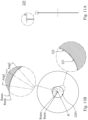
- Fig. 14A is a schematic view of an electronic device 10 according to the 3rd embodiment of the present disclosure.
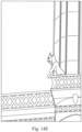
- Fig. 14B is another schematic view of the electronic device 10 according to the 3rd embodiment of Fig. 14A .
- the electronic device 10 is a smartphone.
- the electronic device 10 includes three camera modules 12, 13, 14 and a user interface 11.
- Each of the camera modules 12, 13, 14 includes an imaging lens assembly (figure is omitted) and an image sensor (figure is omitted).
- the image sensor is disposed on an image surface (figure is omitted) of the imaging lens assembly.
- the imaging lens assembly can be the imaging lens assembly according to any one of the aforementioned examples of the 1st embodiment and the 2nd embodiment, but the present disclosure is not limited thereto.
- the camera module 12 is an ultra-wide-angle camera module
- the camera module 13 is a high-pixel camera module
- the camera module 14 is a telephoto camera module
- the user interface 11 is a touch screen, but the present disclosure is not limited thereto.
- the user interface 11 is used to display the screen, and the shooting angle can be manually adjusted to switch between different camera modules 12, 13, 14.
- the camera modules 12, 13, 14 collect an imaging light on the respective image sensor and output electronic signals associated with images to an image signal processor (ISP) 15.
- ISP image signal processor
- the electronic device 10 can further include an optical anti-shake mechanism (figure is omitted). Further, the electronic device 10 can further include at least one focusing assisting module (figure is omitted) and at least one sensing component (figure is omitted).
- the focusing assisting module can be a flash module 16, an infrared distance measurement component, a laser focus module, etc.
- the flash module 16 is for compensating the color temperature.
- the sensing component can have functions for sensing physical momentum and kinetic energies, such as an accelerator, a gyroscope, and a Hall effect element, so as to sense shaking or jitters applied by hands of the user or external environments.
- the autofocus function and the optical anti-shake mechanism of the imaging lens assembly disposed on the electronic device 10 can function to obtain a great image quality and facilitate the electronic device 10 according to the present disclosure to have a capturing function with multiple modes, such as taking optimized selfies, high dynamic range (HDR) with a low light source, 4K resolution recording, etc. Furthermore, the user can visually see the captured image of the camera through the user interface 11 and manually operate the view finding range on the user interface 11 to achieve the auto focus function of what you see is what you get.
- HDR high dynamic range
- the imaging lens assembly, the image sensor, the optical anti-shake mechanism, the sensing component and the focusing assisting module can be disposed on a flexible printed circuit board (FPC) (figure is omitted) and electrically connected to the image signal processor 15 and so on via a connector (figure is omitted) so as to operate a picturing process.
- FPC flexible printed circuit board
- Recent electronic devices such as smartphones have a trend towards thinness and lightness.
- the imaging lens assembly and the related elements are disposed on a FPC and circuits are assembled into a main board of an electronic device by a connector.
- the electronic device 10 can include a plurality of the sensing components and a plurality of the focusing assisting modules, and the sensing components and the focusing assisting modules are disposed on an FPC and another at least one FPC (figure is omitted) and electrically connected to the image signal processor 15 and so on via a corresponding connector so as to operate a picturing process.
- the sensing components and auxiliary optical elements can be disposed on a main board of an electronic device or a board of the other form according to a mechanical design and a requirement of a circuit layout.
- the electronic device 10 can further include, but not be limited to, a display, a control unit, a storage unit, a random-access memory (RAM), a read-only memory (ROM), or the combination thereof.
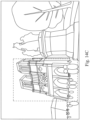
- Fig. 14C is a schematic view of an image captured via the electronic device 10 according to the 3rd embodiment of Fig. 14A .
- a larger ranged image can be captured via the camera module 12 (that is, the ultra-wide-angle camera module), and the camera module 12 has a function for containing more views.
- Fig. 14D is another schematic view of the image captured via the electronic device 10 according to the 3rd embodiment of Fig. 14A .
- a certain ranged and high-pixel image can be captured via the camera module 13 (that is, the high-pixel camera module), and the camera module 13 has a function for high resolution and low distortion.
- Fig. 14E is the other schematic view of the image captured via the electronic device 10 according to the 3rd embodiment of Fig. 14A .
- a far image can be captured and enlarged to a high magnification via the camera module 14 (that is, the telephoto camera module), and the camera module 14 has a function for a high magnification.
- a zoom function of the electronic device 10 can be achieved.
- Fig. 15 is a schematic view of an electronic device 20 according to the 4th embodiment of the present disclosure.
- the electronic device 20 is a smartphone.
- the electronic device 20 includes a plurality of camera modules 21, 22, 23, 24, 25, 26, 27, 28, 29.
- Each of the camera modules 21, 22, 23, 24, 25, 26, 27, 28, 29 includes an imaging lens assembly (figure is omitted) and an image sensor (figure is omitted).
- the image sensor is disposed on an image surface (figure is omitted) of the imaging lens assembly.
- the imaging lens assembly can be the imaging lens assembly according to any one of the aforementioned examples of the 1st embodiment and the 2nd embodiment, but not be limited thereto.
- the camera modules 21, 22 are ultra-wide-angle camera modules
- the camera modules 23, 24 are wide angle camera modules
- the camera modules 25, 26, 27, 28 are telephoto camera modules, wherein the camera modules 27, 28 are configured to fold the light.
- the camera module 29 is a Time-Of-Flight (TOF) module and can further include other types of imaging lens assembly, and it is not limited to the imaging lens assembly of the present disclosure.
- TOF Time-Of-Flight
- the electronic device 20 can further include an optical anti-shake mechanism (figure is omitted). Further, the electronic device 20 can further include at least one focusing assisting module (figure is omitted) and at least one sensing component (figure is omitted).
- the focusing assisting module can be a flash module 20a, an infrared distance measurement component, a laser focus module, etc.
- the flash module 20a is for compensating the color temperature.
- the sensing component can have functions for sensing physical momentum and kinetic energies, such as an accelerator, a gyroscope, and a Hall effect element, so as to sense shaking or jitters applied by hands of the user or external environments.
- the autofocus function and the optical anti-shake mechanism of the imaging lens assembly disposed on the electronic device 20 can function to obtain a great image quality and facilitate the electronic device 20 according to the present disclosure to have a capturing function with multiple modes, such as taking optimized selfies, high dynamic range (HDR) with a low light source, 4K resolution recording, etc.
- HDR high dynamic range
Landscapes
- Physics & Mathematics (AREA)
- General Physics & Mathematics (AREA)
- Optics & Photonics (AREA)
- Optical Elements Other Than Lenses (AREA)
- Lenses (AREA)
- Lens Barrels (AREA)
Abstract
Description
- The present disclosure relates to an imaging lens assembly and an electronic device. More particularly, the present disclosure relates to an imaging lens assembly which can be applied to portable electronic devices.
- In recent years, because the rapid development of portable electronic devices, such as intelligent electronic devices, tablets, etc., are found throughout modern people's whole lives, the imaging lens assemblies applied to portable electronic devices have also flourished. However, with the continuous advancement of technology, users have more requirements for the quality of imaging lens assemblies.
- According to one aspect of the present disclosure, an imaging lens assembly includes a plurality of optical lens elements, a single-piece-formed light blocking sheet and a lens barrel. The single-piece-formed light blocking sheet corresponds to the plurality of optical lens elements. The lens barrel has a circular light-passing hole corresponding to the plurality of optical lens elements and the single-piece-formed light blocking sheet. The single-piece-formed light blocking sheet has a central aperture corresponding to the lens barrel and the plurality of optical lens elements, and a maximum aperture diameter is defined by the central aperture. The single-piece-formed light blocking sheet includes a plurality of light blocking structures surrounding and disposed adjacent to the central aperture, and a number of the plurality of light blocking structures is three to ten. A center of each of the light blocking structures is closer to a center of the central aperture than two ends of each of the light blocking structures, and the two ends of each of the light blocking structures extend toward the maximum aperture diameter of the central aperture. When a maximum aperture radius of the central aperture is Rmax, a minimum inner radius of the central aperture is defined near the center of each of the light blocking structures, the minimum inner radius is Rmin, and a roundness coefficient of the central aperture is tc, the following condition is satisfied: 0.41% ≤ tc ≤ 10.2%, wherein tc = ((Rmax-Rmin)/Rmax)x100%.
- According to the imaging lens assembly of the foregoing aspect, wherein the single-piece-formed light blocking sheet can further include a plurality of radius structures. The plurality of radius structures can surround and be disposed adjacent to the central aperture, and a number of the plurality of radius structures can be three to ten. Each of the radius structures can be connected to two of the light blocking structures adjacent thereto, and each of the radius structures can be arc-shaped.
- According to the imaging lens assembly of the foregoing aspect, wherein when a curvature radius of each of the radius structures is R, the following condition can be satisfied: 0.25 mm < R < 4.2 mm.
- According to the imaging lens assembly of the foregoing aspect, wherein when the maximum aperture radius of the central aperture is Rmax, and a curvature radius of each of the radius structures is R, the following condition can be satisfied: R = Rmax.
- According to the imaging lens assembly of the foregoing aspect, wherein the plurality of radius structures and the plurality of light blocking structures can be disposed alternately and surround the central aperture.
- According to the imaging lens assembly of the foregoing aspect, wherein when a focal length of the imaging lens assembly is f, and the maximum aperture radius of the central aperture is Rmax, the following condition can be satisfied: 0.9 < F < 3.25, wherein F = f/2Rmax.
- According to the imaging lens assembly of the foregoing aspect, wherein the single-piece-formed light blocking sheet can further include a plurality of radius structures, the plurality of radius structures can surround and be disposed adjacent to the central aperture, each of the radius structures can be connected to two of the light blocking structures adjacent thereto, each of the light blocking structures can be a straight-line segment, and each of the radius structures can be arc-shaped.
- According to the imaging lens assembly of the foregoing aspect, wherein when the roundness coefficient of the central aperture is tc, the following condition can be satisfied: 0.83% ≤ tc ≤ 8.6%.
- According to the imaging lens assembly of the foregoing aspect, wherein when the roundness coefficient of the central aperture is tc, the following condition can be satisfied: 0.83% ≤ tc ≤ 6.8%.
- According to the imaging lens assembly of the foregoing aspect, wherein when the roundness coefficient of the central aperture is tc, the following condition can be satisfied: 0.68% ≤ tc ≤ 4.1%.
- According to the imaging lens assembly of the foregoing aspect, wherein the number of the plurality of light blocking structures can be five to nine.
- According to the imaging lens assembly of the foregoing aspect, wherein when a thickness of the single-piece-formed light blocking sheet is S, the following condition can be satisfied: 5 µm < S < 210 µm.
- According to one aspect of the present disclosure, an electronic device includes the imaging lens assembly according to the aforementioned aspect and an image sensor disposed on an image surface of the imaging lens assembly.
- The present disclosure can be more fully understood by reading the following detailed description of the embodiment, with reference made to the accompanying drawings as follows:
-
Fig. 1A is a schematic view of an imaging lens assembly according to the 1st embodiment of the present disclosure. -
Fig. 1B is an exploded view of the imaging lens assembly ofFig. 1A . -
Fig. 2A is a cross-sectional view of a single-piece-formed light blocking sheet of the imaging lens assembly according to the 1st example of the 1st embodiment ofFig. 1A . -
Fig. 2B is a schematic view of the single-piece-formed light blocking sheet ofFig. 2A . -
Fig. 3A is a cross-sectional view of a single-piece-formed light blocking sheet of the imaging lens assembly according to the 2nd example of the 1st embodiment ofFig. 1A . -
Fig. 3B is a schematic view of the single-piece-formed light blocking sheet ofFig. 3A . -
Fig. 4A is a cross-sectional view of a single-piece-formed light blocking sheet of the imaging lens assembly according to the 3rd example of the 1st embodiment ofFig. 1A . -
Fig. 4B is a schematic view of the single-piece-formed light blocking sheet ofFig. 4A . -
Fig. 5A is a cross-sectional view of a single-piece-formed light blocking sheet of the imaging lens assembly according to the 4th example of the 1st embodiment ofFig. 1A . -
Fig. 5B is a schematic view of the single-piece-formed light blocking sheet ofFig. 5A . -
Fig. 6A is a cross-sectional view of a single-piece-formed light blocking sheet of the imaging lens assembly according to the 5th example of the 1st embodiment ofFig. 1A . -
Fig. 6B is a schematic view of the single-piece-formed light blocking sheet ofFig. 6A . -
Fig. 7A is a cross-sectional view of a single-piece-formed light blocking sheet of the imaging lens assembly according to the 6th example of the 1st embodiment ofFig. 1A . -
Fig. 7B is a schematic view of the single-piece-formed light blocking sheet ofFig. 7A . -
Fig. 8A is a cross-sectional view of a single-piece-formed light blocking sheet of the imaging lens assembly according to the 7th example of the 1st embodiment ofFig. 1A . -
Fig. 8B is a schematic view of the single-piece-formed light blocking sheet ofFig. 8A . -
Fig. 9A is a schematic view of an imaging lens assembly according to the 2nd embodiment of the present disclosure. -
Fig. 9B is an exploded view of the imaging lens assembly ofFig. 9A . -
Fig. 10A is a cross-sectional view of a single-piece-formed light blocking sheet of the imaging lens assembly according to the 1st example of the 2nd embodiment ofFig. 9A . -
Fig. 10B is a schematic view of the single-piece-formed light blocking sheet ofFig. 10A . -
Fig. 11A is a cross-sectional view of a single-piece-formed light blocking sheet of the imaging lens assembly according to the 2nd example of the 2nd embodiment ofFig. 9A . -
Fig. 11B is a schematic view of the single-piece-formed light blocking sheet ofFig. 11A . -
Fig. 12A is a cross-sectional view of a single-piece-formed light blocking sheet of the imaging lens assembly according to the 3rd example of the 2nd embodiment ofFig. 9A . -
Fig. 12B is a schematic view of the single-piece-formed light blocking sheet ofFig. 12A . -
Fig. 13A is a cross-sectional view of a single-piece-formed light blocking sheet of the imaging lens assembly according to the 4th example of the 2nd embodiment ofFig. 9A . -
Fig. 13B is a schematic view of the single-piece-formed light blocking sheet ofFig. 13A . -
Fig. 14A is a schematic view of an electronic device according to the 3rd embodiment of the present disclosure. -
Fig. 14B is another schematic view of the electronic device according to the 3rd embodiment ofFig. 14A . -
Fig. 14C is a schematic view of an image captured via the electronic device according to the 3rd embodiment ofFig. 14A . -
Fig. 14D is another schematic view of the image captured via the electronic device according to the 3rd embodiment ofFig. 14A . -
Fig. 14E is the other schematic view of the image captured via the electronic device according to the 3rd embodiment ofFig. 14A . -
Fig. 15 is a schematic view of an electronic device according to the 4th embodiment of the present disclosure. - The present disclosure provides an imaging lens assembly including a plurality of optical lens elements, a single-piece-formed light blocking sheet and a lens barrel. The single-piece-formed light blocking sheet corresponds to the optical lens elements. The lens barrel has a circular light-passing hole corresponding to the optical lens elements and the single-piece-formed light blocking sheet. The single-piece-formed light blocking sheet has a central aperture corresponding to the lens barrel and the optical lens elements, and a maximum aperture diameter is defined by the central aperture. The single-piece-formed light blocking sheet includes a plurality of light blocking structures surrounding and disposed adjacent to the central aperture, and a number of the plurality of light blocking structures is three to ten. A center of each of the light blocking structures is closer to a center of the central aperture than two ends of each of the light blocking structures, and the two ends of each of the light blocking structures extend toward the maximum aperture diameter of the central aperture. When a maximum aperture radius of the central aperture is Rmax, a minimum inner radius of the central aperture is defined near the center of each of the light blocking structures, the minimum inner radius is Rmin, and a roundness coefficient of the central aperture is tc, the following condition is satisfied: 0.41% ≤ tc ≤ 10.2%, wherein tc = ((Rmax-Rmin)/Rmax)×100%. Since the single-piece-formed light blocking sheet can be an aperture stop of the imaging lens assembly, the maximum aperture diameter of the central aperture is equal to an entrance pupil diameter (EPD) of the imaging lens assembly. The single-piece-formed light blocking sheet can have effects similar to that of the multi-blade aperture stop of a single-lens reflex camera, so that the imaging performance of the physical light source can be effectively controlled by the light blocking structures so as to make the light source identifiable, and the size of the central aperture can be precisely controlled to achieve an ideal imaging effect. It should be noted that the roundness coefficient referred to in the present disclosure is not a roundness, and the roundness can be defined as t, wherein t = (Rmax-Rmin).
- The single-piece-formed light blocking sheet can further include a plurality of radius structures, and the plurality of radius structures surround and are disposed adjacent to the central aperture. A number of the plurality of radius structures can be three to ten, each of the radius structures is connected to two of the light blocking structures adjacent thereto, and each of the radius structures can be arc-shaped. Therefore, the arc-shaped arrangement can prevent excessive light blocking and from affecting the specifications of the imaging lens assembly.
- When a curvature radius of each of the radius structures is R, the following condition is satisfied: 0.25 mm < R < 4.2 mm. By controlling the radius structures to maintain a particular quantity, more of the imaging light with a higher field of view can pass through.
- When the maximum aperture radius of the central aperture is Rmax, and a curvature radius of each of the radius structures is R, the following condition is satisfied: R = Rmax. Therefore, the higher f-number of the imaging lens assembly can be maintained under the premise that the identifiability of the light source is maintained.
- The plurality of radius structures and the plurality of light blocking structures are disposed alternately and surround the central aperture. Therefore, by the arrangement that the central aperture includes the radius structures, it is favorable for preventing the excessive length of the light blocking structures.
- When a focal length of the imaging lens assembly is f, and the maximum aperture radius of the central aperture is Rmax, the following condition is satisfied: 0.9 < F < 3.25, wherein F = f/2Rmax. Therefore, within the ideal range of the roundness coefficient, it is favorable for collecting enough amount of the imaging light so as to maintain the imaging criteria at a high level.
- Each of the light blocking structures is a straight-line segment, and each of the radius structures is arc-shaped. Therefore, the concentrated light beam of the strong light source will be reflected by the straight-line light blocking structures at the same time, and the arrangement of the arc-shaped radius structures can prevent excessive light blocking of the strong light source by the straight-line segment, so that the imaging light of the strong light source can pass through completely.
- When the roundness coefficient of the central aperture is tc, the following condition is satisfied: 0.83% ≤ tc ≤ 8.6%. Therefore, it is favorable for preventing excessive light blocking, so that the low-light photography will not be affected. Furthermore, the following condition can be satisfied: 0.83% ≤ tc ≤ 6.8%. Therefore, it is favorable for preventing the imaging light of the weak light source from being affected, and it has better performance when shooting objects with the weak light source. Furthermore, the following condition can be satisfied: 0.68% ≤ tc ≤ 4.1%. Therefore, the amount of incoming light can be increased to ensure better imaging performance for shooting in the night environment.
- The number of the plurality of light blocking structures can be five to nine. Therefore, an appropriate number of the light blocking structures are conducive to maintaining a balance between a high amount of incident light and high quality.
- When a thickness of the single-piece-formed light blocking sheet is S, the following condition is satisfied: 5 µm < S < 210 µm. Therefore, within the specific thickness range, it is not easy to generate additional non-ideal light under the premise of a strict real-shot situation.
- The present disclosure provides an electronic device. The electronic device includes the imaging lens assembly according to the aforementioned aspect and an image sensor disposed on an image surface of the imaging lens assembly.
- According to the above description of the present disclosure, the following specific embodiment and examples are provided for further explanation.
-
Fig. 1A is a schematic view of animaging lens assembly 100 according to the 1st embodiment of the present disclosure.Fig. 1B is an exploded view of theimaging lens assembly 100 ofFig. 1A . As shown inFig. 1A andFig. 1B , theimaging lens assembly 100 includes a plurality of optical lens elements (reference number is omitted), a single-piece-formedlight blocking sheet 120, and alens barrel 101. The plurality of optical lens elements and the single-piece-formedlight blocking sheet 120 are accommodated in thelens barrel 101. Thelens barrel 101 has a circular light-passinghole 110 corresponding to the optical lens elements and the single-piece-formedlight blocking sheet 120. The single-piece-formedlight blocking sheet 120 corresponds to the optical lens elements, and animage surface 102 is located on the most image side of thelens barrel 101. - In detail, in the 1st embodiment of
Fig. 1A , a number of the optical lens elements is five, and the five optical lens elements are, in order from an object side to an image side of theimaging lens assembly 100, a firstoptical lens element 131, a secondoptical lens element 132, a thirdoptical lens element 133, a fourthoptical lens element 134, and a fifthoptical lens element 135. The single-piece-formedlight blocking sheet 120 is a light blocking sheet disposed between thelens barrel 101 and the firstoptical lens element 131 in theimaging lens assembly 100. Further, theimaging lens assembly 100 of the present disclosure can further include other optical elements, such as light blocking sheets, spacers, retainers, etc. In detail, theimaging lens assembly 100 according to the 1st embodiment ofFig. 1A can further include threelight blocking sheets spacer 143, and aretainer 145. It should be noted that the position of the single-piece-formed light blocking sheet and the arrangement of the light blocking sheet, the spacer and the retainer can be adjusted corresponding to the actual needs, and the present disclosure is not limited thereto. -
Fig. 2A is a cross-sectional view of a single-piece-formedlight blocking sheet 120 of theimaging lens assembly 100 according to the 1st example of the 1st embodiment ofFig. 1A .Fig. 2B is a schematic view of the single-piece-formedlight blocking sheet 120 ofFig. 2A . As shown inFig. 2A and Fig. 2B , the single-piece-formedlight blocking sheet 120 has acentral aperture 1201 corresponding to thelens barrel 101 and the optical lens elements. A maximum aperture diameter is defined by thecentral aperture 1201, and a minimum inner radius of thecentral aperture 1201 is defined near a center of each of a plurality oflight blocking structures 121. The single-piece-formedlight blocking sheet 120 includes the plurality oflight blocking structures 121 surrounding and disposed adjacent to thecentral aperture 1201. The center of each of thelight blocking structures 121 is closer to a center of thecentral aperture 1201 than two ends of each of thelight blocking structures 121, and the two ends of each of thelight blocking structures 121 extend toward the maximum aperture diameter of thecentral aperture 1201. InFig. 2B , a number of thelight blocking structures 121 is nine, and when an angle between the connecting lines from the center of thecentral aperture 1201 to the two ends of each of thelight blocking structures 121 is Ang1, Ang1 is 40 degrees, but the present disclosure is not limited thereto. - In the 1st example of the 1st embodiment, when a maximum aperture radius of the
central aperture 1201 is Rmax, the minimum inner radius of thecentral aperture 1201 is Rmin, a roundness coefficient of thecentral aperture 1201 is tc, a thickness of the single-piece-formedlight blocking sheet 120 is S, and a focal length of theimaging lens assembly 100 is f, wherein t = Rmax-Rmin, tc = ((Rmax-Rmin)/Rmax)×100% = t/Rmax×100%, and F = f/2Rmax, the parameters satisfy the conditions shown in Table 1A.Table 1A Rmax (mm) 0.935 S (µm) 16 Rmin (mm) 0.8786 f (mm) 4.16 t 0.0564 F 2.225 tc (%) 6.03 -
Fig. 3A is a cross-sectional view of a single-piece-formedlight blocking sheet 120 of theimaging lens assembly 100 according to the 2nd example of the 1st embodiment ofFig. 1A .Fig. 3B is a schematic view of the single-piece-formedlight blocking sheet 120 ofFig. 3A . As shown inFig. 3A and Fig. 3B , the single-piece-formedlight blocking sheet 120 has acentral aperture 1201 corresponding to thelens barrel 101 and the optical lens elements. A maximum aperture diameter is defined by thecentral aperture 1201, and a minimum inner radius of thecentral aperture 1201 is defined near a center of each of a plurality oflight blocking structures 121. The single-piece-formedlight blocking sheet 120 includes the plurality oflight blocking structures 121 surrounding and disposed adjacent to thecentral aperture 1201. The center of each of thelight blocking structures 121 is closer to a center of thecentral aperture 1201 than two ends of each of thelight blocking structures 121, and the two ends of each of thelight blocking structures 121 extend toward the maximum aperture diameter of thecentral aperture 1201. InFig. 3B , a number of thelight blocking structures 121 is seven, and when an angle between the connecting lines from the center of thecentral aperture 1201 to the two ends of each of thelight blocking structures 121 is Ang1, Ang1 is 51.429 degrees, but the present disclosure is not limited thereto. - In the 2nd example of the 1st embodiment, when a maximum aperture radius of the
central aperture 1201 is Rmax, the minimum inner radius of thecentral aperture 1201 is Rmin, a roundness coefficient of thecentral aperture 1201 is tc, a thickness of the single-piece-formedlight blocking sheet 120 is S, and a focal length of theimaging lens assembly 100 is f, wherein t = Rmax-Rmin, tc = ((Rmax-Rmin)/Rmax)×100% = t/Rmax×100%, and F = f/2Rmax, the parameters satisfy the conditions shown in Table 1B.Table 1B Rmax (mm) 0.935 S (µm) 23 Rmin (mm) 0.8424 f (mm) 4.16 t 0.0926 F 2.225 tc (%) 9.90 -
Fig. 4A is a cross-sectional view of a single-piece-formedlight blocking sheet 120 of theimaging lens assembly 100 according to the 3rd example of the 1st embodiment ofFig. 1A .Fig. 4B is a schematic view of the single-piece-formedlight blocking sheet 120 ofFig. 4A . As shown inFig. 4A and Fig. 4B , the single-piece-formedlight blocking sheet 120 has acentral aperture 1201 corresponding to thelens barrel 101 and the optical lens elements. A maximum aperture diameter is defined by thecentral aperture 1201, and a minimum inner radius of thecentral aperture 1201 is defined near a center of each of a plurality oflight blocking structures 121. The single-piece-formedlight blocking sheet 120 includes the plurality oflight blocking structures 121 and a plurality ofradius structures 122. Thelight blocking structures 121 and theradius structures 122 surround and are disposed adjacent to thecentral aperture 1201, and thelight blocking structures 121 and theradius structures 122 are disposed alternately and surround thecentral aperture 1201. The center of each of thelight blocking structures 121 is closer to a center of thecentral aperture 1201 than two ends of each of thelight blocking structures 121, the two ends of each of thelight blocking structures 121 extend toward the maximum aperture diameter of thecentral aperture 1201, and each of theradius structures 122 is connected to two of thelight blocking structures 121 adjacent thereto. InFig. 4B , a number of thelight blocking structures 121 is seven, and each of thelight blocking structures 121 is a straight-line segment. A number of theradius structures 122 is seven, and each of theradius structures 122 is arc-shaped. When an angle between the connecting lines from the center of thecentral aperture 1201 to the two ends of each of thelight blocking structures 121 is Ang1, Ang1 is 40.002 degrees, but the present disclosure is not limited thereto. When an angle between the connecting lines from the center of thecentral aperture 1201 to the two ends of each of theradius structures 122 is Ang2, Ang2 is 11.426 degrees, but the present disclosure is not limited thereto. - In the 3rd example of the 1st embodiment, when a maximum aperture radius of the
central aperture 1201 is Rmax, the minimum inner radius of thecentral aperture 1201 is Rmin, a roundness coefficient of thecentral aperture 1201 is tc, a thickness of the single-piece-formedlight blocking sheet 120 is S, a focal length of theimaging lens assembly 100 is f, and a curvature radius of each of theradius structures 122 is R, wherein t = Rmax-Rmin, tc = ((Rmax-Rmin)/Rmax)×100% = t/Rmax×100%, and F = f/2Rmax, the parameters satisfy the conditions shown in Table 1C.Table 1C Rmax (mm) 0.935 S (µm) 31 Rmin (mm) 0.8786 f (mm) 4.16 t 0.0564 F 2.225 tc (%) 6.03 R (mm) 0.935 -
Fig. 5A is a cross-sectional view of a single-piece-formedlight blocking sheet 120 of theimaging lens assembly 100 according to the 4th example of the 1st embodiment ofFig. 1A .Fig. 5B is a schematic view of the single-piece-formedlight blocking sheet 120 ofFig. 5A . As shown inFig. 5A and Fig. 5B , the single-piece-formedlight blocking sheet 120 has acentral aperture 1201 corresponding to thelens barrel 101 and the optical lens elements. A maximum aperture diameter is defined by thecentral aperture 1201, and a minimum inner radius of thecentral aperture 1201 is defined near a center of each of a plurality oflight blocking structures 121. The single-piece-formedlight blocking sheet 120 includes the plurality oflight blocking structures 121 and a plurality ofradius structures 122. Thelight blocking structures 121 and theradius structures 122 surround and are disposed adjacent to thecentral aperture 1201, and thelight blocking structures 121 and theradius structures 122 are disposed alternately and surround thecentral aperture 1201. The center of each of thelight blocking structures 121 is closer to a center of thecentral aperture 1201 than two ends of each of thelight blocking structures 121, the two ends of each of thelight blocking structures 121 extend toward the maximum aperture diameter of thecentral aperture 1201, and each of theradius structures 122 is connected to two of thelight blocking structures 121 adjacent thereto. InFig. 5B , a number of thelight blocking structures 121 is five, and each of thelight blocking structures 121 is a straight-line segment. A number of theradius structures 122 is five, and each of theradius structures 122 is arc-shaped. When an angle between the connecting lines from the center of thecentral aperture 1201 to the two ends of each of thelight blocking structures 121 is Ang1, Ang1 is 51.43 degrees, but the present disclosure is not limited thereto. When an angle between the connecting lines from the center of thecentral aperture 1201 to the two ends of each of theradius structures 122 is Ang2, Ang2 is 20.57 degrees, but the present disclosure is not limited thereto. - In the 4th example of the 1st embodiment, when a maximum aperture radius of the
central aperture 1201 is Rmax, the minimum inner radius of thecentral aperture 1201 is Rmin, a roundness coefficient of thecentral aperture 1201 is tc, a thickness of the single-piece-formedlight blocking sheet 120 is S, a focal length of theimaging lens assembly 100 is f, and a curvature radius of each of theradius structures 122 is R, wherein t = Rmax-Rmin, tc = ((Rmax-Rmin)/Rmax)×100% = t/Rmax×100%, and F = f/2Rmax, the parameters satisfy the conditions shown in Table 1D.Table 1D Rmax (mm) 0.935 S (µm) 41 Rmin (mm) 0.8424 f (mm) 4.16 t 0.0926 F 2.225 tc (%) 9.90 R (mm) 0.935 -
Fig. 6A is a cross-sectional view of a single-piece-formedlight blocking sheet 120 of theimaging lens assembly 100 according to the 5th example of the 1st embodiment ofFig. 1A .Fig. 6B is a schematic view of the single-piece-formedlight blocking sheet 120 ofFig. 6A . As shown inFig. 6A and Fig. 6B , the single-piece-formedlight blocking sheet 120 has acentral aperture 1201 corresponding to thelens barrel 101 and the optical lens elements. A maximum aperture diameter is defined by thecentral aperture 1201, and a minimum inner radius of thecentral aperture 1201 is defined near a center of each of a plurality oflight blocking structures 121. The single-piece-formedlight blocking sheet 120 includes the plurality oflight blocking structures 121 and a plurality ofradius structures 122. Thelight blocking structures 121 and theradius structures 122 surround and are disposed adjacent to thecentral aperture 1201, and thelight blocking structures 121 and theradius structures 122 are disposed alternately and surround thecentral aperture 1201. The center of each of thelight blocking structures 121 is closer to a center of thecentral aperture 1201 than two ends of each of thelight blocking structures 121, the two ends of each of thelight blocking structures 121 extend toward the maximum aperture diameter of thecentral aperture 1201, and each of theradius structures 122 is connected to two of thelight blocking structures 121 adjacent thereto. InFig. 6B , a number of thelight blocking structures 121 is five, and each of thelight blocking structures 121 is a straight-line segment. A number of theradius structures 122 is five, and each of theradius structures 122 is arc-shaped. When an angle between the connecting lines from the center of thecentral aperture 1201 to the two ends of each of thelight blocking structures 121 is Ang1, Ang1 is 46.21 degrees, but the present disclosure is not limited thereto. When an angle between the connecting lines from the center of thecentral aperture 1201 to the two ends of each of theradius structures 122 is Ang2, Ang2 is 25.79 degrees, but the present disclosure is not limited thereto. - In the 5th example of the 1st embodiment, when a maximum aperture radius of the
central aperture 1201 is Rmax, the minimum inner radius of thecentral aperture 1201 is Rmin, a roundness coefficient of thecentral aperture 1201 is tc, a thickness of the single-piece-formedlight blocking sheet 120 is S, a focal length of theimaging lens assembly 100 is f, and a curvature radius of each of theradius structures 122 is R, wherein t = Rmax-Rmin, tc = ((Rmax-Rmin)/Rmax)×100% = t/Rmax×100%, and F = f/2Rmax, the parameters satisfy the conditions shown in Table 1E.Table 1E Rmax (mm) 0.935 S (µm) 50 Rmin (mm) 0.86 f (mm) 4.16 t 0.075 F 2.225 tc (%) 8.02 R (mm) 0.935 -
Fig. 7A is a cross-sectional view of a single-piece-formedlight blocking sheet 120 of theimaging lens assembly 100 according to the 6th example of the 1st embodiment ofFig. 1A .Fig. 7B is a schematic view of the single-piece-formedlight blocking sheet 120 ofFig. 7A . As shown inFig. 7A and Fig. 7B , the single-piece-formedlight blocking sheet 120 has acentral aperture 1201 corresponding to thelens barrel 101 and the optical lens elements. A maximum aperture diameter is defined by thecentral aperture 1201, and a minimum inner radius of thecentral aperture 1201 is defined near a center of each of a plurality oflight blocking structures 121. The single-piece-formedlight blocking sheet 120 includes the plurality oflight blocking structures 121 and a plurality ofradius structures 122. Thelight blocking structures 121 and theradius structures 122 surround and are disposed adjacent to thecentral aperture 1201, and thelight blocking structures 121 and theradius structures 122 are disposed alternately and surround thecentral aperture 1201. The center of each of thelight blocking structures 121 is closer to a center of thecentral aperture 1201 than two ends of each of thelight blocking structures 121, the two ends of each of thelight blocking structures 121 extend toward the maximum aperture diameter of thecentral aperture 1201, and each of theradius structures 122 is connected to two of thelight blocking structures 121 adjacent thereto. InFig. 7B , a number of thelight blocking structures 121 is four, and each of thelight blocking structures 121 is a straight-line segment. A number of theradius structures 122 is four, and each of theradius structures 122 is arc-shaped. When an angle between the connecting lines from the center of thecentral aperture 1201 to the two ends of each of thelight blocking structures 121 is Ang1, Ang1 is 51.43 degrees, but the present disclosure is not limited thereto. When an angle between the connecting lines from the center of thecentral aperture 1201 to the two ends of each of theradius structures 122 is Ang2, Ang2 is 38.57 degrees, but the present disclosure is not limited thereto. - In the 6th example of the 1st embodiment, when a maximum aperture radius of the
central aperture 1201 is Rmax, the minimum inner radius of thecentral aperture 1201 is Rmin, a roundness coefficient of thecentral aperture 1201 is tc, a thickness of the single-piece-formedlight blocking sheet 120 is S, a focal length of theimaging lens assembly 100 is f, and a curvature radius of each of theradius structures 122 is R, wherein t = Rmax-Rmin, tc = ((Rmax-Rmin)/Rmax)×100% = t/Rmax×100%, and F = f/2Rmax, the parameters satisfy the conditions shown in Table 1F.Table 1F Rmax (mm) 0.935 S (µm) 100 Rmin (mm) 0.8424 f (mm) 4.16 t 0.0926 F 2.225 tc (%) 9.90 R (mm) 0.935 -
Fig. 8A is a cross-sectional view of a single-piece-formedlight blocking sheet 120 of theimaging lens assembly 100 according to the 7th example of the 1st embodiment ofFig. 1A .Fig. 8B is a schematic view of the single-piece-formedlight blocking sheet 120 ofFig. 8A . As shown inFig. 8A and Fig. 8B , the single-piece-formedlight blocking sheet 120 has acentral aperture 1201 corresponding to thelens barrel 101 and the optical lens elements. A maximum aperture diameter is defined by thecentral aperture 1201, and a minimum inner radius of thecentral aperture 1201 is defined near a center of each of a plurality oflight blocking structures 121. The single-piece-formedlight blocking sheet 120 includes the plurality oflight blocking structures 121 and a plurality ofradius structures 122. Thelight blocking structures 121 and theradius structures 122 surround and are disposed adjacent to thecentral aperture 1201, and thelight blocking structures 121 and theradius structures 122 are disposed alternately and surround thecentral aperture 1201. The center of each of thelight blocking structures 121 is closer to a center of thecentral aperture 1201 than two ends of each of thelight blocking structures 121, the two ends of each of thelight blocking structures 121 extend toward the maximum aperture diameter of thecentral aperture 1201, and each of theradius structures 122 is connected to two of thelight blocking structures 121 adjacent thereto. InFig. 8B , a number of thelight blocking structures 121 is four, and each of thelight blocking structures 121 is a straight-line segment. A number of theradius structures 122 is four, and each of theradius structures 122 is arc-shaped. When an angle between the connecting lines from the center of thecentral aperture 1201 to the two ends of each of thelight blocking structures 121 is Ang1, Ang1 is 42.965 degrees, but the present disclosure is not limited thereto. When an angle between the connecting lines from the center of thecentral aperture 1201 to the two ends of each of theradius structures 122 is Ang2, Ang2 is 47.035 degrees, but the present disclosure is not limited thereto. - In the 7th example of the 1st embodiment, when a maximum aperture radius of the
central aperture 1201 is Rmax, the minimum inner radius of thecentral aperture 1201 is Rmin, a roundness coefficient of thecentral aperture 1201 is tc, a thickness of the single-piece-formedlight blocking sheet 120 is S, a focal length of theimaging lens assembly 100 is f, and a curvature radius of each of theradius structures 122 is R, wherein t = Rmax-Rmin, tc = ((Rmax-Rmin)/Rmax)×100% = t/Rmax×100%, and F = f/2Rmax, the parameters satisfy the conditions shown in Table 1G.Table 1G Rmax (mm) 0.935 S (µm) 31 Rmin (mm) 0.87 f (mm) 4.16 t 0.065 F 2.225 tc (%) 6.95 R (mm) 0.935 -
Fig. 9A is a schematic view of animaging lens assembly 200 according to the 2nd embodiment of the present disclosure.Fig. 9B is an exploded view of theimaging lens assembly 200 ofFig. 9A . As shown inFig. 9A andFig. 9B , theimaging lens assembly 200 includes a plurality of optical lens elements (reference number is omitted), a single-piece-formedlight blocking sheet 220, and alens barrel 201. The plurality of optical lens elements and the single-piece-formedlight blocking sheet 220 are accommodated in thelens barrel 201. Thelens barrel 201 has a circular light-passinghole 210 corresponding to the optical lens elements and the single-piece-formedlight blocking sheet 220. The single-piece-formedlight blocking sheet 220 corresponds to the optical lens elements, and animage surface 202 is located on the most image side of thelens barrel 201. - In the 2nd embodiment of
Fig. 9A , a number of the optical lens elements is seven, and the seven optical lens elements are, in order from an object side to an image side of theimaging lens assembly 200, a firstoptical lens element 231, a secondoptical lens element 232, a thirdoptical lens element 233, a fourthoptical lens element 234, a fifthoptical lens element 235, a sixthoptical lens element 236, and a seventhoptical lens element 237. The single-piece-formedlight blocking sheet 220 is a light blocking sheet disposed between the secondoptical lens element 232 and the thirdoptical lens element 233 in theimaging lens assembly 200. Further, theimaging lens assembly 200 of the present disclosure can further include other optical elements, such as light blocking sheets, spacers, retainers, etc. In detail, theimaging lens assembly 200 according to the 2nd embodiment ofFig. 9A can further include fivelight blocking sheets spacer 245, and aretainer 247. It should be noted that the position of the single-piece-formed light blocking sheet and the arrangement of the light blocking sheet, the spacer and the retainer can be adjusted corresponding to the actual needs, and the present disclosure is not limited thereto. Furthermore, theimaging lens assembly 200 can further include afilter 203, wherein thefilter 203 is disposed between thelens barrel 201 and theimage surface 202. -
Fig. 10A is a cross-sectional view of a single-piece-formedlight blocking sheet 220 of theimaging lens assembly 200 according to the 1st example of the 2nd embodiment ofFig. 9A .Fig. 10B is a schematic view of the single-piece-formedlight blocking sheet 220 ofFig. 10A . As shown inFig. 10A and Fig. 10B , the single-piece-formedlight blocking sheet 220 has acentral aperture 2201 corresponding to thelens barrel 201 and the optical lens elements. A maximum aperture diameter is defined by thecentral aperture 2201, and a minimum inner radius of thecentral aperture 2201 is defined near a center of each of a plurality oflight blocking structures 221. The single-piece-formedlight blocking sheet 220 includes the plurality oflight blocking structures 221 surrounding and disposed adjacent to thecentral aperture 2201. The center of each of thelight blocking structures 221 is closer to a center of thecentral aperture 2201 than two ends of each of thelight blocking structures 221, and the two ends of each of thelight blocking structures 221 extend toward the maximum aperture diameter of thecentral aperture 2201. InFig. 10B , a number of thelight blocking structures 221 is nine, and when an angle between the connecting lines from the center of thecentral aperture 2201 to the two ends of each of thelight blocking structures 221 is Ang1, Ang1 is 40 degrees, but the present disclosure is not limited thereto. - In the 1st example of the 2nd embodiment, when a maximum aperture radius of the
central aperture 2201 is Rmax, the minimum inner radius of thecentral aperture 2201 is Rmin, a roundness coefficient of thecentral aperture 2201 is tc, a thickness of the single-piece-formedlight blocking sheet 220 is S, and a focal length of theimaging lens assembly 200 is f, wherein t = Rmax-Rmin, tc = ((Rmax-Rmin)/Rmax)x100% = t/Rmax×100%, and F = f/2Rmax, the parameters satisfy the conditions shown in Table 2A.Table 2A Rmax (mm) 0.7485 S (µm) 16 Rmin (mm) 0.7033 f (mm) 3.05 t 0.0452 F 2.038 tc (%) 6.04 -
Fig. 11A is a cross-sectional view of a single-piece-formedlight blocking sheet 220 of theimaging lens assembly 200 according to the 2nd example of the 2nd embodiment ofFig. 9A .Fig. 11B is a schematic view of the single-piece-formedlight blocking sheet 220 ofFig. 11A . As shown inFig. 11A and Fig. 11B , the single-piece-formedlight blocking sheet 220 has acentral aperture 2201 corresponding to thelens barrel 201 and the optical lens elements. A maximum aperture diameter is defined by thecentral aperture 2201, and a minimum inner radius of thecentral aperture 2201 is defined near a center of each of a plurality oflight blocking structures 221. The single-piece-formedlight blocking sheet 220 includes the plurality oflight blocking structures 221 and a plurality ofradius structures 222. Thelight blocking structures 221 and theradius structures 222 surround and are disposed adjacent to thecentral aperture 2201, and thelight blocking structures 221 and theradius structures 222 are disposed alternately and surround thecentral aperture 2201. The center of each of thelight blocking structures 221 is closer to a center of thecentral aperture 2201 than two ends of each of thelight blocking structures 221, the two ends of each of thelight blocking structures 221 extend toward the maximum aperture diameter of thecentral aperture 2201, and each of theradius structures 222 is connected to two of thelight blocking structures 221 adjacent thereto. InFig. 11B , a number of thelight blocking structures 221 is nine, and each of thelight blocking structures 221 is a straight-line segment. A number of theradius structures 222 is nine, and each of theradius structures 222 is arc-shaped. When an angle between the connecting lines from the center of thecentral aperture 2201 to the two ends of each of thelight blocking structures 221 is Ang1, Ang1 is 23.086 degrees, but the present disclosure is not limited thereto. When an angle between the connecting lines from the center of thecentral aperture 2201 to the two ends of each of theradius structures 222 is Ang2, Ang2 is 16.914 degrees, but the present disclosure is not limited thereto. - In the 2nd example of the 2nd embodiment, when a maximum aperture radius of the
central aperture 2201 is Rmax, the minimum inner radius of thecentral aperture 2201 is Rmin, a roundness coefficient of thecentral aperture 2201 is tc, a thickness of the single-piece-formedlight blocking sheet 220 is S, a focal length of theimaging lens assembly 200 is f, and a curvature radius of each of theradius structures 222 is R, wherein t = Rmax-Rmin, tc = ((Rmax-Rmin)/Rmax)×100% = t/Rmax×100%, and F = f/2Rmax, the parameters satisfy the conditions shown in Table 2B.Table 2B Rmax (mm) 0.7485 S (µm) 23 Rmin (mm) 0.7333 f (mm) 3.05 t 0.0152 F 2.038 tc (%) 2.03 R (mm) 0.7485 -
Fig. 12A is a cross-sectional view of a single-piece-formedlight blocking sheet 220 of theimaging lens assembly 200 according to the 3rd example of the 2nd embodiment ofFig. 9A .Fig. 12B is a schematic view of the single-piece-formedlight blocking sheet 220 ofFig. 12A . As shown inFig. 12A and Fig. 12B , the single-piece-formedlight blocking sheet 220 has acentral aperture 2201 corresponding to thelens barrel 201 and the optical lens elements. A maximum aperture diameter is defined by thecentral aperture 2201, and a minimum inner radius of thecentral aperture 2201 is defined near a center of each of a plurality oflight blocking structures 221. The single-piece-formedlight blocking sheet 220 includes the plurality oflight blocking structures 221 surrounding and disposed adjacent to thecentral aperture 2201. The center of each of thelight blocking structures 221 is closer to a center of thecentral aperture 2201 than two ends of each of thelight blocking structures 221, and the two ends of each of thelight blocking structures 221 extend toward the maximum aperture diameter of thecentral aperture 2201. InFig. 12B , a number of thelight blocking structures 221 is seven, and when an angle between the connecting lines from the center of thecentral aperture 2201 to the two ends of each of thelight blocking structures 221 is Ang1, Ang1 is 51.429 degrees, but the present disclosure is not limited thereto. - In the 3rd example of the 2nd embodiment, when a maximum aperture radius of the
central aperture 2201 is Rmax, the minimum inner radius of thecentral aperture 2201 is Rmin, a roundness coefficient of thecentral aperture 2201 is tc, a thickness of the single-piece-formedlight blocking sheet 220 is S, and a focal length of theimaging lens assembly 200 is f, wherein t = Rmax-Rmin, tc = ((Rmax-Rmin)/Rmax)×100% = t/Rmax×100%, and F = f/2Rmax, the parameters satisfy the conditions shown in Table 2C.Table 2C Rmax (mm) 0.7485 S (µm) 41 Rmin (mm) 0.6743 f (mm) 3.05 t 0.0742 F 2.038 tc (%) 9.91 -
Fig. 13A is a cross-sectional view of a single-piece-formedlight blocking sheet 220 of theimaging lens assembly 200 according to the 4th example of the 2nd embodiment ofFig. 9A .Fig. 13B is a schematic view of the single-piece-formedlight blocking sheet 220 ofFig. 13A . As shown inFig. 13A and Fig. 13B , the single-piece-formedlight blocking sheet 220 has acentral aperture 2201 corresponding to thelens barrel 201 and the optical lens elements. A maximum aperture diameter is defined by thecentral aperture 2201, and a minimum inner radius of thecentral aperture 2201 is defined near a center of each of a plurality oflight blocking structures 221. The single-piece-formedlight blocking sheet 220 includes the plurality oflight blocking structures 221 and a plurality ofradius structures 222. Thelight blocking structures 221 and theradius structures 222 surround and are disposed adjacent to thecentral aperture 2201, and thelight blocking structures 221 and theradius structures 222 are disposed alternately and surround thecentral aperture 2201. The center of each of thelight blocking structures 221 is closer to a center of thecentral aperture 2201 than two ends of each of thelight blocking structures 221, the two ends of each of thelight blocking structures 221 extend toward the maximum aperture diameter of thecentral aperture 2201, and each of theradius structures 222 is connected to two of thelight blocking structures 221 adjacent thereto. InFig. 13B , a number of thelight blocking structures 221 is seven, and each of thelight blocking structures 221 is a straight-line segment. A number of theradius structures 222 is seven, and each of theradius structures 222 is arc-shaped. When an angle between the connecting lines from the center of thecentral aperture 2201 to the two ends of each of thelight blocking structures 221 is Ang1, Ang1 is 22.294 degrees, but the present disclosure is not limited thereto. When an angle between the connecting lines from the center of thecentral aperture 2201 to the two ends of each of theradius structures 222 is Ang2, Ang2 is 29.135 degrees, but the present disclosure is not limited thereto. - In the 4th example of the 2nd embodiment, when a maximum aperture radius of the
central aperture 2201 is Rmax, the minimum inner radius of thecentral aperture 2201 is Rmin, a roundness coefficient of thecentral aperture 2201 is tc, a thickness of the single-piece-formedlight blocking sheet 220 is S, a focal length of theimaging lens assembly 200 is f, and a curvature radius of each of theradius structures 222 is R, wherein t = Rmax-Rmin, tc = ((Rmax-Rmin)/Rmax)×100% = t/Rmax×100%, and F = f/2Rmax, the parameters satisfy the conditions shown in Table 2D.Table 2D Rmax (mm) 0.7485 S (µm) 50 Rmin (mm) 0.7343 f (mm) 3.05 t 0.0142 F 2.038 tc (%) 1.90 R (mm) 0.7485 -
Fig. 14A is a schematic view of anelectronic device 10 according to the 3rd embodiment of the present disclosure.Fig. 14B is another schematic view of theelectronic device 10 according to the 3rd embodiment ofFig. 14A . As shown inFig. 14A andFig. 14B , theelectronic device 10 is a smartphone. Theelectronic device 10 includes threecamera modules user interface 11. Each of thecamera modules camera module 12 is an ultra-wide-angle camera module, thecamera module 13 is a high-pixel camera module, thecamera module 14 is a telephoto camera module, and theuser interface 11 is a touch screen, but the present disclosure is not limited thereto. - A user enters a shooting mode via the
user interface 11. Theuser interface 11 is used to display the screen, and the shooting angle can be manually adjusted to switch betweendifferent camera modules camera modules - As shown in
Fig. 14A andFig. 14B , according to the camera specifications of theelectronic device 10, theelectronic device 10 can further include an optical anti-shake mechanism (figure is omitted). Further, theelectronic device 10 can further include at least one focusing assisting module (figure is omitted) and at least one sensing component (figure is omitted). The focusing assisting module can be aflash module 16, an infrared distance measurement component, a laser focus module, etc. Theflash module 16 is for compensating the color temperature. The sensing component can have functions for sensing physical momentum and kinetic energies, such as an accelerator, a gyroscope, and a Hall effect element, so as to sense shaking or jitters applied by hands of the user or external environments. Thus the autofocus function and the optical anti-shake mechanism of the imaging lens assembly disposed on theelectronic device 10 can function to obtain a great image quality and facilitate theelectronic device 10 according to the present disclosure to have a capturing function with multiple modes, such as taking optimized selfies, high dynamic range (HDR) with a low light source, 4K resolution recording, etc. Furthermore, the user can visually see the captured image of the camera through theuser interface 11 and manually operate the view finding range on theuser interface 11 to achieve the auto focus function of what you see is what you get. - Furthermore, the imaging lens assembly, the image sensor, the optical anti-shake mechanism, the sensing component and the focusing assisting module can be disposed on a flexible printed circuit board (FPC) (figure is omitted) and electrically connected to the
image signal processor 15 and so on via a connector (figure is omitted) so as to operate a picturing process. Recent electronic devices such as smartphones have a trend towards thinness and lightness. The imaging lens assembly and the related elements are disposed on a FPC and circuits are assembled into a main board of an electronic device by a connector. Hence, it can fulfill a mechanical design of a limited inner space of the electronic device and a requirement of a circuit layout and obtain a larger allowance, and it is also favorable for an autofocus function of the imaging lens assembly obtaining a flexible control via a touch screen of the electronic device. In the 3rd embodiment, theelectronic device 10 can include a plurality of the sensing components and a plurality of the focusing assisting modules, and the sensing components and the focusing assisting modules are disposed on an FPC and another at least one FPC (figure is omitted) and electrically connected to theimage signal processor 15 and so on via a corresponding connector so as to operate a picturing process. In other embodiments (figure is omitted), the sensing components and auxiliary optical elements can be disposed on a main board of an electronic device or a board of the other form according to a mechanical design and a requirement of a circuit layout. - Furthermore, the
electronic device 10 can further include, but not be limited to, a display, a control unit, a storage unit, a random-access memory (RAM), a read-only memory (ROM), or the combination thereof. -
Fig. 14C is a schematic view of an image captured via theelectronic device 10 according to the 3rd embodiment ofFig. 14A . As shown inFig. 14C , a larger ranged image can be captured via the camera module 12 (that is, the ultra-wide-angle camera module), and thecamera module 12 has a function for containing more views. -
Fig. 14D is another schematic view of the image captured via theelectronic device 10 according to the 3rd embodiment ofFig. 14A . As shown inFig. 14D , a certain ranged and high-pixel image can be captured via the camera module 13 (that is, the high-pixel camera module), and thecamera module 13 has a function for high resolution and low distortion. -
Fig. 14E is the other schematic view of the image captured via theelectronic device 10 according to the 3rd embodiment ofFig. 14A . As shown inFig. 14E , a far image can be captured and enlarged to a high magnification via the camera module 14 (that is, the telephoto camera module), and thecamera module 14 has a function for a high magnification. - As shown in
Fig. 14C to Fig. 14E , when an image is captured viadifferent camera modules electronic device 10 can be achieved. -
Fig. 15 is a schematic view of anelectronic device 20 according to the 4th embodiment of the present disclosure. As shown inFig. 15 , theelectronic device 20 is a smartphone. Theelectronic device 20 includes a plurality ofcamera modules camera modules camera modules camera modules camera modules camera modules camera module 29 is a Time-Of-Flight (TOF) module and can further include other types of imaging lens assembly, and it is not limited to the imaging lens assembly of the present disclosure. - According to the camera specifications of the
electronic device 20, theelectronic device 20 can further include an optical anti-shake mechanism (figure is omitted). Further, theelectronic device 20 can further include at least one focusing assisting module (figure is omitted) and at least one sensing component (figure is omitted). The focusing assisting module can be aflash module 20a, an infrared distance measurement component, a laser focus module, etc. Theflash module 20a is for compensating the color temperature. The sensing component can have functions for sensing physical momentum and kinetic energies, such as an accelerator, a gyroscope, and a Hall effect element, so as to sense shaking or jitters applied by hands of the user or external environments. Thus the autofocus function and the optical anti-shake mechanism of the imaging lens assembly disposed on theelectronic device 20 can function to obtain a great image quality and facilitate theelectronic device 20 according to the present disclosure to have a capturing function with multiple modes, such as taking optimized selfies, high dynamic range (HDR) with a low light source, 4K resolution recording, etc. - Further, all of other structures and dispositions according to the 4th embodiment are the same as the structures and the dispositions according to the 3rd embodiment, and will not be described again herein.
Claims (13)
- An imaging lens assembly (100), characterized in comprising:a plurality of optical lens elements (131, 132, 133, 134, 135);a single-piece-formed light blocking sheet (120) corresponding to the plurality of optical lens elements (131, 132, 133, 134, 135); anda lens barrel (101) having a circular light-passing hole (110) corresponding to the plurality of optical lens elements (131, 132, 133, 134, 135) and the single-piece-formed light blocking sheet (120);wherein the single-piece-formed light blocking sheet (120) has a central aperture (1201) corresponding to the lens barrel (101) and the plurality of optical lens elements (131, 132, 133, 134, 135), a maximum aperture diameter is defined by the central aperture (1201), the single-piece-formed light blocking sheet (120) comprises a plurality of light blocking structures (121) surrounding and disposed adjacent to the central aperture (1201), a number of the plurality of light blocking structures (121) is three to ten, a center of each of the light blocking structures (121) is closer to a center of the central aperture (1201) than two ends of each of the light blocking structures (121), and the two ends of each of the light blocking structures (121) extend toward the maximum aperture diameter of the central aperture (1201);wherein a maximum aperture radius of the central aperture (1201) is Rmax, a minimum inner radius of the central aperture (1201) is defined near the center of each of the light blocking structures (121), the minimum inner radius is Rmin, a roundness coefficient of the central aperture (1201) is tc, and the following condition is satisfied:

- The imaging lens assembly (100) of claim 1, wherein the single-piece-formed light blocking sheet (120) further comprises a plurality of radius structures (122), the plurality of radius structures (122) surround and are disposed adjacent to the central aperture (1201), a number of the plurality of radius structures (122) is three to ten, each of the radius structures (122) is connected to two of the light blocking structures (121) adjacent thereto, and each of the radius structures (122) is arc-shaped.
- The imaging lens assembly (100) of claim 2, wherein a curvature radius of each of the radius structures (122) is R, and the following condition is satisfied:

- The imaging lens assembly (100) of claims 2 or 3, wherein the maximum aperture radius of the central aperture (1201) is Rmax, a curvature radius of each of the radius structures (122) is R, and the following condition is satisfied:

- The imaging lens assembly (100) of any one of claims 2 to 4, wherein the plurality of radius structures (122) and the plurality of light blocking structures (121) are disposed alternately and surround the central aperture (1201).
- The imaging lens assembly (100) of any one of claims 1 to 5, wherein a focal length of the imaging lens assembly (100) is f, the maximum aperture radius of the central aperture (1201) is Rmax, and the following condition is satisfied:

- The imaging lens assembly (100) of any one of claims 1 to 6, wherein the single-piece-formed light blocking sheet (120) further comprises a plurality of radius structures (122), the plurality of radius structures (122) surround and are disposed adjacent to the central aperture (1201), each of the radius structures (122) is connected to two of the light blocking structures (121) adjacent thereto, each of the light blocking structures (121) is a straight-line segment, and each of the radius structures (122) is arc-shaped.
- The imaging lens assembly (100) of any one of claims 1 to 7, wherein the roundness coefficient of the central aperture (1201) is tc, and the following condition is satisfied:

- The imaging lens assembly (100) of any one of claims 1 to 8, wherein the roundness coefficient of the central aperture (1201) is tc, and the following condition is satisfied:

- The imaging lens assembly (100) of any one of claims 1 to 9, wherein the roundness coefficient of the central aperture (1201) is tc, and the following condition is satisfied:

- The imaging lens assembly (100) of any one of claims 1 to 10, wherein the number of the plurality of light blocking structures (121) is five to nine.
- The imaging lens assembly (100) of any one of claims 1 to 11, wherein a thickness of the single-piece-formed light blocking sheet (120) is S, and the following condition is satisfied:

- An electronic device (10), characterized in comprising:the imaging lens assembly (100) of any one of claims 1 to 12; andan image sensor, wherein the image sensor is disposed on an image surface (102) of the imaging lens assembly (100).
Applications Claiming Priority (1)
| Application Number | Priority Date | Filing Date | Title |
|---|---|---|---|
| US202263328757P | 2022-04-08 | 2022-04-08 |
Publications (2)
| Publication Number | Publication Date |
|---|---|
| EP4276500A1 true EP4276500A1 (en) | 2023-11-15 |
| EP4276500B1 EP4276500B1 (en) | 2026-03-04 |
Family
ID=85873808
Family Applications (1)
| Application Number | Title | Priority Date | Filing Date |
|---|---|---|---|
| EP23166472.3A Active EP4276500B1 (en) | 2022-04-08 | 2023-04-04 | Imaging lens assembly and electronic device |
Country Status (4)
| Country | Link |
|---|---|
| US (1) | US12541072B2 (en) |
| EP (1) | EP4276500B1 (en) |
| CN (2) | CN116893488B (en) |
| TW (1) | TWI829423B (en) |
Families Citing this family (1)
| Publication number | Priority date | Publication date | Assignee | Title |
|---|---|---|---|---|
| TWI829423B (en) * | 2022-04-08 | 2024-01-11 | 大立光電股份有限公司 | Imaging lens assembly and electronic device |
Citations (5)
| Publication number | Priority date | Publication date | Assignee | Title |
|---|---|---|---|---|
| JP2014206768A (en) * | 2014-08-06 | 2014-10-30 | リコーイメージング株式会社 | Diaphragm device and optical instrument including the same |
| US20180196171A1 (en) * | 2017-01-12 | 2018-07-12 | Largan Precision Co., Ltd. | Optical lens assembly, imaging lens module and electronic apparatus |
| US20200301246A1 (en) * | 2019-03-21 | 2020-09-24 | Samsung Electro-Mechanics Co., Ltd. | Aperture module, camera module, and portable electronic device |
| US20210080623A1 (en) * | 2019-09-12 | 2021-03-18 | Largan Precision Co., Ltd. | Imaging optical element set, imaging lens assemly and electronic device |
| US20210364675A1 (en) * | 2020-05-25 | 2021-11-25 | Zhejiang Sunny Optics Co., Ltd. | Light blocking sheet and lens module |
Family Cites Families (21)
| Publication number | Priority date | Publication date | Assignee | Title |
|---|---|---|---|---|
| JP2002258132A (en) * | 2001-03-05 | 2002-09-11 | Olympus Optical Co Ltd | Camera |
| CN101292194B (en) * | 2005-11-04 | 2012-07-11 | 松下电器产业株式会社 | Imaging device and camera |
| JP5037639B2 (en) * | 2010-02-23 | 2012-10-03 | シャープ株式会社 | Imaging module |
| KR101444526B1 (en) | 2012-07-27 | 2014-09-24 | 삼성전기주식회사 | Lens module |
| TWM490029U (en) | 2014-06-13 | 2014-11-11 | Largan Precision Co Ltd | Light shielding plate, optical lens system and mobile device |
| US9400383B2 (en) | 2014-12-10 | 2016-07-26 | Newmax Technology Co., Ltd. | Light blocking plate and lens assembly including the same |
| TWM521747U (en) | 2015-10-16 | 2016-05-11 | 大立光電股份有限公司 | Shading sheet, shading element, optical element, imaging lens and lens module |
| TWI625544B (en) * | 2016-07-21 | 2018-06-01 | 先進光電科技股份有限公司 | Optical image capturing system |
| CN112433419B (en) * | 2017-02-24 | 2022-03-25 | 大立光电股份有限公司 | Shading sheet, optical lens group, imaging lens and electronic device |
| JP7207327B2 (en) * | 2017-12-28 | 2023-01-18 | ソニーグループ株式会社 | Imaging lens and imaging device |
| CN110501795A (en) * | 2018-05-18 | 2019-11-26 | 南昌欧菲精密光学制品有限公司 | Lens set and lens module |
| JP6921041B2 (en) * | 2018-07-26 | 2021-08-18 | 富士フイルム株式会社 | Imaging lens and imaging device |
| JP2020106725A (en) * | 2018-12-28 | 2020-07-09 | マクセル株式会社 | Light shield, lens unit and camera module |
| TWI696857B (en) * | 2019-04-29 | 2020-06-21 | 大立光電股份有限公司 | Imaging lens module with plastic barrel and electronic device including same module |
| TWI704404B (en) * | 2019-05-15 | 2020-09-11 | 大陽科技股份有限公司 | Camera module and electronic device |
| TWI759835B (en) * | 2020-05-20 | 2022-04-01 | 大立光電股份有限公司 | Imaging lens assembly module, camera module and electronic device |
| CN111781704B (en) * | 2020-07-20 | 2025-09-09 | 江西欧菲光学有限公司 | Imaging lens, image capturing module and electronic equipment |
| CN111856716A (en) * | 2020-08-13 | 2020-10-30 | 天津欧菲光电有限公司 | Optical system, camera module, electronic equipment and automobile |
| TWI812062B (en) * | 2021-11-05 | 2023-08-11 | 大立光電股份有限公司 | Optical lens assembly and electronic device |
| TWI813249B (en) * | 2021-12-28 | 2023-08-21 | 大立光電股份有限公司 | Lens assembly, camera module and electronic device |
| TWI829423B (en) * | 2022-04-08 | 2024-01-11 | 大立光電股份有限公司 | Imaging lens assembly and electronic device |
-
2022
- 2022-11-11 TW TW111143229A patent/TWI829423B/en active
-
2023
- 2023-02-10 CN CN202310101389.8A patent/CN116893488B/en active Active
- 2023-02-10 CN CN202320199717.8U patent/CN219392350U/en not_active Withdrawn - After Issue
- 2023-03-30 US US18/192,837 patent/US12541072B2/en active Active
- 2023-04-04 EP EP23166472.3A patent/EP4276500B1/en active Active
Patent Citations (5)
| Publication number | Priority date | Publication date | Assignee | Title |
|---|---|---|---|---|
| JP2014206768A (en) * | 2014-08-06 | 2014-10-30 | リコーイメージング株式会社 | Diaphragm device and optical instrument including the same |
| US20180196171A1 (en) * | 2017-01-12 | 2018-07-12 | Largan Precision Co., Ltd. | Optical lens assembly, imaging lens module and electronic apparatus |
| US20200301246A1 (en) * | 2019-03-21 | 2020-09-24 | Samsung Electro-Mechanics Co., Ltd. | Aperture module, camera module, and portable electronic device |
| US20210080623A1 (en) * | 2019-09-12 | 2021-03-18 | Largan Precision Co., Ltd. | Imaging optical element set, imaging lens assemly and electronic device |
| US20210364675A1 (en) * | 2020-05-25 | 2021-11-25 | Zhejiang Sunny Optics Co., Ltd. | Light blocking sheet and lens module |
Also Published As
| Publication number | Publication date |
|---|---|
| US20230324645A1 (en) | 2023-10-12 |
| CN116893488B (en) | 2026-01-30 |
| TW202340839A (en) | 2023-10-16 |
| CN116893488A (en) | 2023-10-17 |
| US12541072B2 (en) | 2026-02-03 |
| CN219392350U (en) | 2023-07-21 |
| TWI829423B (en) | 2024-01-11 |
| BR102023006597A2 (en) | 2023-10-24 |
| EP4276500B1 (en) | 2026-03-04 |
Similar Documents
| Publication | Publication Date | Title |
|---|---|---|
| US12216246B2 (en) | Miniature telephoto lens module and a camera utilizing such a lens module | |
| US12429751B2 (en) | Imaging lens assembly module, camera module and electronic device | |
| CN105408806B (en) | Slim Dual Aperture Zoom Digital Camera | |
| CN108873246A (en) | Imaging lens group with plastic lens, imaging lens module and electronic device | |
| US20200310073A1 (en) | Imaging lens module and electronic device | |
| CN117555191A (en) | Light shielding structure and imaging lens module | |
| EP4276500B1 (en) | Imaging lens assembly and electronic device | |
| US20260126648A1 (en) | Imaging lens assembly and electronic device | |
| EP4163691A1 (en) | Imaging optical system, camera module and electronic device | |
| US12111484B2 (en) | Imaging lens assembly, image capturing apparatus and electronic device | |
| EP4379461A1 (en) | Imaging lens assembly module, camera module and electronic device | |
| KR20220136021A (en) | Lenses and mobile terminals | |
| US20250264785A1 (en) | Light-folded camera module and electronic device | |
| US20250389925A1 (en) | Image lens element, imaging lens assembly and electronic device | |
| US20240310607A1 (en) | Imaging lens assembly, camera module and electronic device | |
| EP4485034A2 (en) | Light path folding element, camera module and electronic device | |
| US20250013038A1 (en) | Imaging lens assembly module, camera module and electronic device | |
| US20260063880A1 (en) | Plastic optical folding element, imaging lens module and electronic device |
Legal Events
| Date | Code | Title | Description |
|---|---|---|---|
| PUAI | Public reference made under article 153(3) epc to a published international application that has entered the european phase |
Free format text: ORIGINAL CODE: 0009012 |
|
| STAA | Information on the status of an ep patent application or granted ep patent |
Free format text: STATUS: REQUEST FOR EXAMINATION WAS MADE |
|
| 17P | Request for examination filed |
Effective date: 20230404 |
|
| AK | Designated contracting states |
Kind code of ref document: A1 Designated state(s): AL AT BE BG CH CY CZ DE DK EE ES FI FR GB GR HR HU IE IS IT LI LT LU LV MC ME MK MT NL NO PL PT RO RS SE SI SK SM TR |
|
| GRAP | Despatch of communication of intention to grant a patent |
Free format text: ORIGINAL CODE: EPIDOSNIGR1 |
|
| STAA | Information on the status of an ep patent application or granted ep patent |
Free format text: STATUS: GRANT OF PATENT IS INTENDED |
|
| RIC1 | Information provided on ipc code assigned before grant |
Ipc: G02B 5/00 20060101AFI20250828BHEP Ipc: G02B 7/02 20210101ALI20250828BHEP Ipc: G02B 27/00 20060101ALI20250828BHEP Ipc: G03B 9/06 20210101ALI20250828BHEP Ipc: G03B 9/08 20210101ALI20250828BHEP Ipc: G03B 30/00 20210101ALI20250828BHEP |
|
| INTG | Intention to grant announced |
Effective date: 20250930 |
|
| GRAS | Grant fee paid |
Free format text: ORIGINAL CODE: EPIDOSNIGR3 |
|
| GRAA | (expected) grant |
Free format text: ORIGINAL CODE: 0009210 |
|
| STAA | Information on the status of an ep patent application or granted ep patent |
Free format text: STATUS: THE PATENT HAS BEEN GRANTED |
|
| P01 | Opt-out of the competence of the unified patent court (upc) registered |
Free format text: CASE NUMBER: UPC_APP_0001505_4276500/2026 Effective date: 20260116 |
|
| AK | Designated contracting states |
Kind code of ref document: B1 Designated state(s): AL AT BE BG CH CY CZ DE DK EE ES FI FR GB GR HR HU IE IS IT LI LT LU LV MC ME MK MT NL NO PL PT RO RS SE SI SK SM TR |
|
| REG | Reference to a national code |
Ref country code: CH Ref legal event code: F10 Free format text: ST27 STATUS EVENT CODE: U-0-0-F10-F00 (AS PROVIDED BY THE NATIONAL OFFICE) Effective date: 20260304 Ref country code: GB Ref legal event code: FG4D |
|
| REG | Reference to a national code |
Ref country code: IE Ref legal event code: FG4D |
|
| REG | Reference to a national code |
Ref country code: DE Ref legal event code: R096 Ref document number: 602023012833 Country of ref document: DE |
|
| REG | Reference to a national code |
Ref country code: NL Ref legal event code: FP |