EP4274107A1 - System with multiple nfc-chips - Google Patents
System with multiple nfc-chips Download PDFInfo
- Publication number
- EP4274107A1 EP4274107A1 EP22172119.4A EP22172119A EP4274107A1 EP 4274107 A1 EP4274107 A1 EP 4274107A1 EP 22172119 A EP22172119 A EP 22172119A EP 4274107 A1 EP4274107 A1 EP 4274107A1
- Authority
- EP
- European Patent Office
- Prior art keywords
- nfc
- antenna
- circuit
- detuning
- matching network
- Prior art date
- Legal status (The legal status is an assumption and is not a legal conclusion. Google has not performed a legal analysis and makes no representation as to the accuracy of the status listed.)
- Granted
Links
Images




Classifications
-
- H—ELECTRICITY
- H04—ELECTRIC COMMUNICATION TECHNIQUE
- H04B—TRANSMISSION
- H04B5/00—Near-field transmission systems, e.g. inductive or capacitive transmission systems
- H04B5/20—Near-field transmission systems, e.g. inductive or capacitive transmission systems characterised by the transmission technique; characterised by the transmission medium
- H04B5/24—Inductive coupling
-
- H—ELECTRICITY
- H04—ELECTRIC COMMUNICATION TECHNIQUE
- H04B—TRANSMISSION
- H04B5/00—Near-field transmission systems, e.g. inductive or capacitive transmission systems
- H04B5/20—Near-field transmission systems, e.g. inductive or capacitive transmission systems characterised by the transmission technique; characterised by the transmission medium
- H04B5/24—Inductive coupling
- H04B5/26—Inductive coupling using coils
- H04B5/266—One coil at each side, e.g. with primary and secondary coils
-
- H—ELECTRICITY
- H04—ELECTRIC COMMUNICATION TECHNIQUE
- H04B—TRANSMISSION
- H04B5/00—Near-field transmission systems, e.g. inductive or capacitive transmission systems
- H04B5/40—Near-field transmission systems, e.g. inductive or capacitive transmission systems characterised by components specially adapted for near-field transmission
- H04B5/45—Transponders
-
- H—ELECTRICITY
- H04—ELECTRIC COMMUNICATION TECHNIQUE
- H04B—TRANSMISSION
- H04B5/00—Near-field transmission systems, e.g. inductive or capacitive transmission systems
- H04B5/20—Near-field transmission systems, e.g. inductive or capacitive transmission systems characterised by the transmission technique; characterised by the transmission medium
- H04B5/24—Inductive coupling
- H04B5/26—Inductive coupling using coils
-
- H—ELECTRICITY
- H04—ELECTRIC COMMUNICATION TECHNIQUE
- H04B—TRANSMISSION
- H04B5/00—Near-field transmission systems, e.g. inductive or capacitive transmission systems
- H04B5/70—Near-field transmission systems, e.g. inductive or capacitive transmission systems specially adapted for specific purposes
-
- H—ELECTRICITY
- H04—ELECTRIC COMMUNICATION TECHNIQUE
- H04B—TRANSMISSION
- H04B5/00—Near-field transmission systems, e.g. inductive or capacitive transmission systems
- H04B5/70—Near-field transmission systems, e.g. inductive or capacitive transmission systems specially adapted for specific purposes
- H04B5/79—Near-field transmission systems, e.g. inductive or capacitive transmission systems specially adapted for specific purposes for data transfer in combination with power transfer
Definitions
- the present disclosure relates to the field of Near Field Communication (NFC) and particularly to circuits, methods, and devices used in connection with Near Field Communication (NFC).
- NFC Near Field Communication
- NFC Near Field Communication
- NFC denotes a standardized data transmission technique for the contactless exchange of data across relatively short distances (e.g. a few centimeters) using electromagnetically coupled inductors.
- NFC is based on the well-known RFID technique and allows data rates of several hundred kBits/s.
- Currently NFC is commonly used in the field of "Micropayment" (non-cash payments of small amounts) as well as in the field of access control.
- Further applications include, for example, the transmission of authentication data in the process of establishing a communication link via, for example, Bluetooth, Wireless LAN or the like.
- Recently sensor applications have been developed which allow retrieving measured data, e.g. by a mobile device, using NFC.
- NFC is standardized in ISO/IEC 18092 (Near Field Communication Interface and Protocol-1) and ISO/IEC 21481 (Near Field Communication Interface and Protocol-2).
- NFC transceivers In order to perform the mentioned payment functions, many mobile devices such as smart phones are equipped with NFC transceivers. Such devices are usually referred to as NFC enabled devices or NFC readers. Their counterparts are often referred to as NFC tags or NFC transponders. NFC transponders usually do not have their own energy supply and source the electrical energy required for their operation from the electromagnetic field used for NFC (NFC field).
- the NFC field is usually generated by the NFC reader (e.g. a smart phone). That is, energy is transferred via the NFC field from the NFC reader to an NFC transponder, whereas data transmission is possible in both directions.
- Most of the circuitry of an NFC transponder required to implement Near Field Communication is integrated in a single chip.
- NFC readers can also emulate an NFC tag. That is, an NFC reader can behave like a passive NFC transponder communicating with another NFC reader. In such cases, the NFC reader is also referred to as NFC controller.
- An NFC tag can be implemented, by an NFC reader/controller, using a so-called secure element (which is a piece of hardware) or by a software application executed by a controller.
- So-called smart cards such as bank cards (credit card, debit card), ID cards, insurance cards or the like may also be emulated by software, which is also known as Host Card Emulation (HCE).
- HCE Host Card Emulation
- NFC data transfers for payments are mainly realized via a so-called "secure element" stored in the operating system of the (NFC enabled) mobile device.
- This allows to implement, for example, mobile applications for payment services independently of third parties, i.e. without the need for the usual physical smart card.
- the antennas of NFC readers and NFC tags/transponders are usually simple conductor loops which can be formed, e.g., on a printed circuit board (PCB).
- PCB printed circuit board
- the corresponding antenna circuits are usually operated at the same resonance frequency, which results in a maximum electromagnetic coupling.
- the voltage induced in the antenna of the NFC transponder is at its maximum.
- the resonance frequency is usually at 13.56 MHz.
- the NFC chip of an NFC transponder is usually configured to generate its own supply voltage from the NFC field. However, there are also transponders with their own supply (e.g. provided by a battery).
- WLC 2.0 Wireless Charging 2.0 has been designed to make it easier and more convenient to charge devices such as, for examples, wearables (e.g. earbuds, smartwatches, fitness trackers, etc.), headsets, smart locks and other products.
- Such products may include more than one NFC tag (or one NFC reader and at least one NFC tag), wherein one NFC tag may be coupled to a battery to charge the battery using WLC technology.
- wearables e.g. earbuds, smartwatches, fitness trackers, etc.
- headsets e.g. earbuds, smartwatches, fitness trackers, etc.
- Such products may include more than one NFC tag (or one NFC reader and at least one NFC tag), wherein one NFC tag may be coupled to a battery to charge the battery using WLC technology.
- two NFC chips reader and two or more tags
- NFC chips reader and tag
- a more specific problem may arise when one NFC chip is activated for wireless charging.
- the relatively high signal levels received by an NFC antenna may be harmful for other NFC devices not designed for wireless charging.
- the inventors have identified a need for improvement of NFC techniques in order to allow more than two NFC chips which share the same physical communication channel and are thus inductively coupled.
- the NFC device includes a first NFC antenna and a second NFC antenna, which are inductively coupled to each other (and, during operation, also to the antenna of a further NFC device).
- the NFC device further includes a first NFC circuit coupled to the first antenna via a first matching network and a second NFC circuit coupled to the second antenna via a second matching network.
- the NFC device includes a first detuning circuit coupled to the first antenna and configured to, when activated, detune a first resonant circuit including the first antenna and the first matching circuit.
- the method includes the detuning of a first resonant circuit including a first antenna and a first matching network of an NFC device, wherein the first antenna is coupled to the first matching network and a first NFC circuit of the NFC device.
- the method further includes receiving data - by a second NFC circuit of the NFC device and from a further NFC device - via a second antenna coupled to a second matching network and the second NFC circuit, wherein the first antenna and the second antenna are inductively coupled to each.
- the detuning of the first resonant circuit is stopped dependent on the received data.
- the method includes the detuning of a first resonant circuit including a first antenna and a first matching network of an NFC device, wherein the first antenna is coupled to the first matching network and a first NFC circuit of the NFC device.
- the method further includes receiving data - by a second NFC circuit of the NFC device and from a further NFC device - via a second antenna coupled to a second matching network and the second NFC circuit, wherein the first antenna and the second antenna are inductively coupled to each.
- the detuning of the first resonant circuit is stopped when a supply voltage of the NFC device falls below a threshold value.
- NFC Near Field Communication
- an NFC enabled device 2 including an NFC reader
- an NFC circuit 1 e.g. integrated in an NFC chip
- NFC tag/transponder e.g. a RFID tag
- RFID tag e.g. a RFID tag
- NFC communication interface e.g. a sensor circuit
- NFC is not only used for (e.g. bidirectional) data transmission but also for the (unidirectional) transmission of energy from the NFC reader 2 to the NFC chip 1.
- NFC chip 1 may also be used to charge a battery using the NFC wireless charging (WLC) technique, wherein the energy received by the NFC antenna is used to charge the battery.
- the antennas of the NFC chip 1 and the NFC reader 2 are usually implemented using conductor loops (i.e. flat coils), and the data transmission, as well as the energy transmission, are based on the inductive coupling of the two antennas.
- NFC chips may be employed in various applications.
- NFC may be used for authentication, in payment systems, access control systems, smart locks or the like.
- NFC also began to be used in more complex applications such as, for example, sensor applications, to provide a communication link between sensor electronics (e.g. included in the NFC chip 1) and an NFC enabled device, which can then be used for the digital post processing and/or for the display, on a screen of the NFC enabled device (e.g. a smart phone or tablet PC), of the measured data provided by the sensor electronics.
- sensor electronics e.g. included in the NFC chip 1
- an NFC enabled device e.g. a smart phone or tablet PC
- the NFC chip (transponder) only needs to be active for a relatively short time. More complex applications may include electronic circuits that consume more power for longer time periods as compared to normal NFC transponders. In such applications, the NFC transponders may need a separate power supply such as a battery, as the NFC field generated by the NFC reader is not able to transmit enough energy to reliably operate the NFC transponder. To recharge the battery, the NFC WLC technology may be used, which usually requires a dedicated NFC chip which is capable of energy harvesting in accordance with the NFC WLC standard.
- the examples described herein relate to a situation, in which one device includes two NFC chips, wherein one of the NFC chips is used for wireless charging and the other one of the NFC chips is used to implement an NFC reader or an NFC tag.
- an NFC reader NFC controller
- This device (which includes two NFC chips) can communicate with another NFC enabled device or NFC tag. This situation is illustrated in Fig. 2 and further explained below.
- the circuit shown in Fig. 2 represents a system including two NFC circuits 11 and 12 (e.g. integrated into two NFC chips) which share one NFC antenna 3. That is, the first NFC chip 11 and the second NFC chip 12 are coupled to the NFC antenna 3 via an RF switch 30.
- the acronym RF stands for "radio frequency", wherein current NFC systems use 13.56 MHz signals.
- the first NFC chip 11 is configured to be used for wireless charging of the battery 5
- the second NFC chip 12 is an NFC tag configured to be used for wireless payment.
- the controller 10 is configured, inter alia, to connect the NFC antenna 3 with either the second NFC chip 12 or the first NFC chip 11.
- Fig. 2 is a simplification and various components which are not relevant for the present discussion have been omitted.
- Matching circuits which are used for impedance matching, and coupled between the NFC antenna and the NFC chips are not shown in Fig. 3 . It may be assumed that the matching circuits are included in the NFC chips 11 and 12.
- the charging electronics battery charger
- the NFC enabled device which can communicate with either the NFC chip 11 or the NFC chip 12. The concept illustrated in Fig. 2 allows the NFC chips 11 and 12 to share one antenna but requires the RF switch 30.
- the RF chip 30 To connect the NFC antenna 3 with one of the NFC chips, the RF chip 30 needs a voltage supply provided by the battery 5. In a situation, in which the battery 5 is discharged and not able to provide a sufficient voltage to operate the RF switch 30, the RF switch 30 is inoperative, and, as a consequence, NFC and wireless charging cannot be used.
- Fig. 3 illustrates, by way of example, another concept which allows to combine two or more NFC chips in one system / device while avoiding the need for an RF switch.
- the circuit of Fig. 3 has two NFC antennas 3a and 3b, wherein antenna 3a is coupled with NFC circuit 11 via a matching circuit 110 and antenna 3b is coupled with NFC circuit 12 via a matching circuit 120.
- the matching circuits may also be included in the NFC chips but are depicted, in Fig. 3 , as separate component as the matching circuits are relevant for the further discussion.
- the NFC circuits 11 and 12 may include an NFC transceiver and be integrated in respective NFC chips.
- the two antennas 3a and 3b are inductively coupled. They may be implemented as (e.g. at least partly overlapping) flat coils in different wiring layers of a printed circuit board (PCB). Alternatively, they may be implemented in the same wiring layer adjacent to each other.
- the matching circuits 110 and 120 may include a passive impedance adjustment network composed of a plurality of capacitances and, optionally, a filter network (to eliminate electromagnetic interferences, EMI) which may be a passive LC low-pass filter composed of capacitors and inductances.
- EMI electromagnetic interferences
- the matching circuits 110 and 120 are usually designed such that - together with the respective antennas 3a, 3b - form resonant circuits whose resonant frequency matches at least approximately the oscillation frequency of the NFC field, which is 13.56 MHz in many applications.
- the resonant circuits may include further elements such as resistor for the purpose of damping.
- a capacitor C A may be connected to the matching circuit 110 (also referred to as matching network) using an electronic switch SW A such that the capacitor C A is connected in parallel to the antenna 3a when the electronic switch SW A is closed (capacitor C A active). Accordingly, the capacitor C A is disconnected from the matching network 110 when the electronic switch SW A is open (capacitor C A inactive).
- the capacitor C A can also be regarded as part of the matching circuit 110, wherein - while active - the capacitor C A has the effect that the resonant circuit formed by antenna 3a, matching circuit 110 and capacitor C A is detuned by activating the capacitor C A (i.e. by closing the switch SW A ).
- the resonance frequency may be shifted from 13.56 MHz (capacitor C A inactive, switch SW A open) to, e.g. 25 MHz (capacitor C A active, switch SW A closed) with the effect that the NFC circuit/chip 11 cannot receive data via the NFC antenna 3a and is practically decoupled from the NFC antenna 3a and thus from the NFC communication channel.
- the capacitor C A and the electronic switch SW A can be regarded as a detuning circuit, which can be activated and deactivated by a control signal S A that controls the state of the switch SW A .
- the detuning circuit may be more complex than in the example of Fig. 3 and include further passive electronic components such as capacitors, inductors, and resistors.
- the switch SW A may include more than one switching element that may be implemented as, for example, transistors.
- the detuning circuit is coupled to the antenna 3a and configured to, when activated, detune a resonance frequency of a resonant circuit formed by the antenna 3a, the respective matching circuit 110 and the detuning circuit (formed by C A , and SW A in the example of Fig. 3 ).
- the electronic switch SW A can be closed/opened, by the NFC chip 12, to activate/deactivate the capacitor C A .
- the NFC circuit/chip 12 which is coupled to the antenna 3b via the matching circuit 120, is capable of detuning the other matching circuit 110, which is arranged between antenna 3a and NFC chip 11.
- the NFC chip 12 needs a supply voltage V B provided by battery 5 to operate. As long as the battery 5 is able to provide a sufficiently high supply voltage V B (i.e.
- the NFC chip 12 can detune the matching circuit 110 of NFC chip 11 (by closing switch SW A ), and therefore can use the NFC antenna 3b to communicate with an NFC enabled device (not shown in Fig. 3 ), wherein the NFC chip 11 is not able to interfere due to the detuned matching circuit 110. Accordingly, the NFC chip 12 may provide the desired function, e.g. operate as NFC reader or as NFC tag, as long as the battery 5 provides the required supply voltage V B .
- the switch SW A is open/inactive and, consequently, the matching circuit 110 is not detuned anymore.
- the NFC chip 11 is able to communicate with an external NFC enabled device (not shown in Fig. 3 ) using antenna 3a.
- the NFC chip 11 is used for the wireless charging of the battery 5.
- an empty battery leads to an activation of the NFC chip 11 (because the respective matching circuit 110 cannot be detuned anymore) thus allowing wireless charging, whereas in the previous example of Fig. 2 an empty battery makes the device inoperative as the RF switch 30 disconnects the shared antenna from both NFC chips.
- Fig. 3 is merely one illustrative example of the concept of deactivating the matching circuit of an NFC chip in order to prevent this NFC chip to disturb the communication between another NFC chip and an external NFC enabled device or NFC tag.
- the entity, which controls the switch SW A is not necessarily the NFC chip 12.
- any other entity e.g. a control circuit, a battery monitoring circuit, etc.
- a loss of voltage supply e.g.
- the matching circuit 110 being tuned, so that NFC chip 11 is be able to communicate with an external NFC enabled device (cf. device 2 in Fig. 1 , not shown in Fig. 3 ), wherein the NFC chip 11 is able to generate its own supply voltage from the electromagnetic power of the NFC field generated by the external NFC enabled device. As discussed above, this voltage supply (generated from the NFC field) may be used to recharge the battery 5.
- the NFC chip 12 is inactive if the battery 5 does not provide a sufficient supply voltage.
- the NFC chip 12 may be an NFC reader or an NFC tag, which may be emulated by an NFC reader.
- the NFC chip 12 may also be a conventional NFC transponder which generates its own supply from an NFC field generated by an external NFC enabled device.
- the matching circuit 110 is not detuned (because switch SW A is open due to a lack of supply), and the NFC chip 11 receives energy (via antenna 3a) to recharge the battery, the signal level received by the antenna 3b may be too high and exceed the absolute maximum rating of NFC chip 12.
- a switch SW B may be arranged between the antenna 3b and the NFC chip 12 as shown in the example of Fig. 4 .
- Fig. 4 is basically the same as the example of Fig. 3 , wherein the only additional component in Fig. 4 is the switch SW B which is configured to connect and disconnect the antenna 3b from the NFC chip 12.
- the switch SW B is controlled by the NFC chip 12.
- a different entity e.g. a control circuit, a battery monitoring circuit, etc.
- the switches are SW A and SW B are closed.
- the antenna 3b is connected to the matching network 120 and thus to the NFC chip 12, whereas the matching network 110 is detuned as explained above.
- the switches are SW A and SW B are open (which is their default state).
- the antenna 3b is disconnected from the matching network 120 and NFC chip 12, and the matching network 110 is not detuned anymore, thus allowing the NFC chip 11 to provide energy for the recharging of the battery 5 using WLC technology.
- the NFC chip 12 is protected from high signal levels by the (open) switch SW B .
- Fig. 5 illustrates an alternative to the example of Fig. 4 .
- the circuits of Fig. 4 and 5 are the same except that the antenna 3b is not disconnected from the NFC chip 12 using a switch, but instead the antenna 3b (to be precise: the resonant circuit formed by antenna and matching circuit) is detuned by connecting a capacitor C B in parallel to the antenna 3b by closing the switch SW B .
- Capacitor C B and switch SW B form a detuning circuit in the same way as explained above with reference to capacitor C A and switch SW A .
- the switch SW B is closed to detune the antenna 3a when the NFC chip 11 is active, e.g. to harvest energy for recharging the battery 5.
- the detuning of the antenna 3a can be done in the same way as explained above with reference to Fig. 4 .
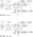
- the circuit arrangement of Fig. 5 is further discussed with reference to Figs. 6A and 6B which illustrate how the circuit arrangement of Fig. 5 may be used in a wireless payment application.
- the circuit arrangement may be included in a wearable device such as a fitness tracker, a smart watch or the like.
- the NFC chip 12 is an NFC controller connected to a secure element 13 and a controller 10 (host controller).
- the NFC chip 12 controls the switch SW A to detune the antenna 3a of NFC chip 11, which practically deactivates the NFC chip 11 (which therefore does not detune the antenna 3b).
- the NFC enabled device 2 may be a payment terminal, which includes a conventional NFC reader configured for the processing of NFC payment.
- the NFC chip 12 (NFC controller) emulates an NFC tag as it may also be included in credit cards or the like.
- the operation of the NFC chip 12 may be controlled by the host controller 10.
- Fig. 6B shows a situation, in which the NFC chip 12 is inactive and does not detune the antenna 3a of NFC chip 11, which therefore may be used to (re-) charge the battery 5.
- the NFC chip 12 may be inactive, for example, due to a low supply voltage V B caused by a low state of charge (SoC) of the battery 5.
- SoC state of charge
- the NFC chip 11 receives (harvests) energy provided by the NFC field which is generated by the NFC enabled device. This energy may be used to charge the battery 5 in accordance with the NFC WLC standard.
- a low supply voltage V B is not the only situation, in which wireless charging can be used.
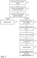
- the NFC chip 12 When the NFC chip 12 is active (as illustrated in Fig. 6A ) and receives a charging request instead of a payment request, the NFC chip 12 may transition into a quiet mode and stop detuning the NFC chip 11 thus allowing wireless charging in the same way as it is the case when the battery 5 is empty. The process is further illustrated by the flow chart of Fig. 7 .
- Fig. 7 starts with the NFC chip 12 being active and listening (see Fig. 7 , reference sign S1).
- the NFC chip 12 detunes (see Fig. 7 , ref. sign S2) the antenna 3a of the NFC chip 11 as shown in Fig. 6A .
- the NFC chip 12 receives a request (see Fig. 7 , ref. sign S3), which may be either a payment request or a charging request).
- the NFC chip 11 is not able to interfere with the communication as its antenna is detuned.
- the payment process is completed (see Fig. 7 , ref. sign S4).
- the payment process is as such known and thus not further discussed herein.
- the NFC chip 12 responds with a message indicating - to the NFC enabled device which sent the request - that WLC is not available ("not WLC compliant" message, see Fig. 7 , ref. sign S5), stops detuning the antenna 3a of NFC chip 11 (see Fig. 7 , ref. sign S6), and enters a quiet mode, in which any communication on the NFC channel is ignored (see Fig. 7 , ref. sign S7).
- the NFC chip 11 can become active, detune the antenna 3b of NFC chip 12 (optional, see Fig. 7 , ref. sign S8), and complete the charging process (see Fig. 7 , ref.
- the NFC chip 11 stops detuning of antenna 3a and may trigger a "wakeup" of NFC chip 12 (see Fig. 7 , ref. sign S10), which then leaves the quiet mode and again enter the normal mode, in which NFC chip 12 is listening and ready to receive another request (see Fig. 7 , ref. sign S1).
- the detuning of antenna 3b is optional, in particular when the antenna 3b can be disconnected from NFC chip 12 as discussed above with reference to Fig. 4 .
- NFC payment is merely an illustrative example, and the NFC chip 12 may have a different purpose or function.
- the NFC chip 11 is not necessarily an NFC WLC chip but can have any other purpose or function. Irrespective of the particular function of the NFC chips 11 and 12, one NFC chip may act as "master" NFC chip and detune the antenna of the other NFC chip in order to avoid the other chip from interfering with the communication between the master NFC chip and an external NFC enabled device.
- Fig. 8 illustrates another application, wherein the circuit shown in Fig. 8 (8A and 8B ) is basically the same as in Fig. 4 , wherein, in the present example, the NFC chip 12 may be configured as an NFC reader.
- the example of Fig 8 may be used in an access control application, e.g. in a device which controls an electromechanical lock ("smart lock"), a (garage) door opener or the like.
- the NFC chip 12 may communicate with the controller 10 which may trigger, for example, the opening of the door, once the authentication was successful.
- the NFC chip 12 is configured as NFC reader which generates an NFC field via antenna 3b.
- the NFC chip 12 controls the switch SW B to connect antenna 3b with matching network 120 and the switch SW A to detune the antenna 3a of NFC chip 11. If a user places an NFC transponder 5 close enough to the antenna 3b, NFC chip 12 and NFC transponder 5 can communicate to authenticate the owner of the NFC transponder 5.
- the controller 10 may, for example, drive an electromechanical lock as mentioned above.
- the SoC State of Charge
- the NFC chip 12 becomes inoperative. As a consequence, the switches SW B and SW A open thus disconnecting antenna 3b and stop detuning of antenna 3a. This situation is shown in Fig. 8B .
- a user can place any suitable NFC enabled device 2 close to the antennas 3a and 3b.
- the NFC enabled device 2 generates an electromagnetic field which, due to the inductive coupling, induces a current in NFC antenna 3a.
- the NFC chip 11 can start its normal operation and initiate a charging process in accordance with the NFC WLC standard. Once the charging process is completed, the SoC of battery 5 is high enough to provide the required supply voltage VB to operate the NFC reader 12.
- Fig. 9 is a flow chart illustrating, by way of example, the function of the circuit of Fig. 5 .
- the mode of operation or state of the NFC device depends on whether the battery of the NFC device provides a sufficient supply voltage ( FIG. 9 , box M1, see also Fig. 5 , battery 5). If this is the case, the first detuning circuit (see Fig. 5 , switch SW A , capacitor C A ) for detuning the first NFC chip (see Fig. 5 , NFC chip 11) is active ( Fig. 9 , box M2). As a consequence, a normal communication is possible between the second NFC chip (see Fig. 5 , NFC chip 12) and an external NFC device (e.g.
- this communication may be initiated by the second NFC chip (if the external NFC device is an NFC transponder/tag) or by the external NFC device. In the latter case, the second NFC chip may emulate an NFC tag as explained above.
- the first detuning circuit for detuning the first NFC chip (see Fig. 5 , NFC chip 11) is inactive ( Fig. 9 , box M4).
- the second NFC chip (see Fig. 5 , NFC chip 12) may be inactive due to lack of supply.
- the first NFC chip can start detuning the antenna of the second NFC chip ( Fig. 9 , box M5). This detuning is optional and has basically the purpose of protection the inactive second NFC chip.
- the protection may also be achieved by disconnecting the antenna from the second NFC chip as shown in the examples of Fig. 4 and 8 . In some applications such a protection mechanism may not be necessary.
- the power received from the external NFC enabled device may be used for recharging the battery and the first NFC chip can initiate the wireless charging process ( Fig. 9 , box M6). Once the battery has sufficient charge and the charging process is completed, the second NFC chip 12 may become again activate (resulting in a reactivation of the first detuning circuit).
Landscapes
- Engineering & Computer Science (AREA)
- Computer Networks & Wireless Communication (AREA)
- Signal Processing (AREA)
- Near-Field Transmission Systems (AREA)
- Power Engineering (AREA)
Abstract
Description
- The present disclosure relates to the field of Near Field Communication (NFC) and particularly to circuits, methods, and devices used in connection with Near Field Communication (NFC).
- Near Field Communication (NFC) denotes a standardized data transmission technique for the contactless exchange of data across relatively short distances (e.g. a few centimeters) using electromagnetically coupled inductors. NFC is based on the well-known RFID technique and allows data rates of several hundred kBits/s. Currently NFC is commonly used in the field of "Micropayment" (non-cash payments of small amounts) as well as in the field of access control. Further applications include, for example, the transmission of authentication data in the process of establishing a communication link via, for example, Bluetooth, Wireless LAN or the like. Recently sensor applications have been developed which allow retrieving measured data, e.g. by a mobile device, using NFC. NFC is standardized in ISO/IEC 18092 (Near Field Communication Interface and Protocol-1) and ISO/IEC 21481 (Near Field Communication Interface and Protocol-2).
- In order to perform the mentioned payment functions, many mobile devices such as smart phones are equipped with NFC transceivers. Such devices are usually referred to as NFC enabled devices or NFC readers. Their counterparts are often referred to as NFC tags or NFC transponders. NFC transponders usually do not have their own energy supply and source the electrical energy required for their operation from the electromagnetic field used for NFC (NFC field). The NFC field is usually generated by the NFC reader (e.g. a smart phone). That is, energy is transferred via the NFC field from the NFC reader to an NFC transponder, whereas data transmission is possible in both directions. Most of the circuitry of an NFC transponder required to implement Near Field Communication is integrated in a single chip.
- In many applications NFC readers can also emulate an NFC tag. That is, an NFC reader can behave like a passive NFC transponder communicating with another NFC reader. In such cases, the NFC reader is also referred to as NFC controller. An NFC tag can be implemented, by an NFC reader/controller, using a so-called secure element (which is a piece of hardware) or by a software application executed by a controller. So-called smart cards such as bank cards (credit card, debit card), ID cards, insurance cards or the like may also be emulated by software, which is also known as Host Card Emulation (HCE). HCE is a basically a piece of software that represents a virtual copy of the smart card. For example, NFC data transfers for payments are mainly realized via a so-called "secure element" stored in the operating system of the (NFC enabled) mobile device. This allows to implement, for example, mobile applications for payment services independently of third parties, i.e. without the need for the usual physical smart card.
- The antennas of NFC readers and NFC tags/transponders are usually simple conductor loops which can be formed, e.g., on a printed circuit board (PCB). In antenna circuits such conductor loops represent respective inductors which form, in connection with corresponding capacitors, resonant circuits. For an efficient energy transfer from an NFC enabled device to an NFC transponder, the corresponding antenna circuits are usually operated at the same resonance frequency, which results in a maximum electromagnetic coupling. As a consequence, the voltage induced in the antenna of the NFC transponder is at its maximum. In standard applications, the resonance frequency is usually at 13.56 MHz. The NFC chip of an NFC transponder is usually configured to generate its own supply voltage from the NFC field. However, there are also transponders with their own supply (e.g. provided by a battery).
- Recently (Oct. 2021), the NFC Forum, which promotes standardization of NFC technologies, released the Wireless Charging (WLC) specification 2.0. WLC 2.0 has been designed to make it easier and more convenient to charge devices such as, for examples, wearables (e.g. earbuds, smartwatches, fitness trackers, etc.), headsets, smart locks and other products. Such products may include more than one NFC tag (or one NFC reader and at least one NFC tag), wherein one NFC tag may be coupled to a battery to charge the battery using WLC technology. However, once more than two NFC chips (reader and two or more tags) are inductively coupled (i.e. share the same physical communication channel), a communication between two particular NFC chips (reader and tag) may be disturbed by one of the other NFC chips. A more specific problem may arise when one NFC chip is activated for wireless charging. The relatively high signal levels received by an NFC antenna may be harmful for other NFC devices not designed for wireless charging.
- The inventors have identified a need for improvement of NFC techniques in order to allow more than two NFC chips which share the same physical communication channel and are thus inductively coupled.
- The problem indicated above is solved by the NFC device of
claim 1 as well as the methods ofclaims 12 and 16. Various embodiments and further developments are covered by the dependent claims. - An NFC device is described herein. According to one exemplary embodiment, the NFC device includes a first NFC antenna and a second NFC antenna, which are inductively coupled to each other (and, during operation, also to the antenna of a further NFC device). The NFC device further includes a first NFC circuit coupled to the first antenna via a first matching network and a second NFC circuit coupled to the second antenna via a second matching network. Furthermore, the NFC device includes a first detuning circuit coupled to the first antenna and configured to, when activated, detune a first resonant circuit including the first antenna and the first matching circuit.
- Furthermore, a method for a NFC device is described herein. In accordance with one exemplary embodiment the method includes the detuning of a first resonant circuit including a first antenna and a first matching network of an NFC device, wherein the first antenna is coupled to the first matching network and a first NFC circuit of the NFC device. The method further includes receiving data - by a second NFC circuit of the NFC device and from a further NFC device - via a second antenna coupled to a second matching network and the second NFC circuit, wherein the first antenna and the second antenna are inductively coupled to each. The detuning of the first resonant circuit is stopped dependent on the received data.
- In accordance with a further exemplary embodiment the method includes the detuning of a first resonant circuit including a first antenna and a first matching network of an NFC device, wherein the first antenna is coupled to the first matching network and a first NFC circuit of the NFC device. The method further includes receiving data - by a second NFC circuit of the NFC device and from a further NFC device - via a second antenna coupled to a second matching network and the second NFC circuit, wherein the first antenna and the second antenna are inductively coupled to each. The detuning of the first resonant circuit is stopped when a supply voltage of the NFC device falls below a threshold value.
- The invention can be better understood with reference to the following drawings and descriptions. The components in the figures are not necessarily to scale; instead emphasis is placed upon illustrating the principles of the invention. Moreover, in the figures, like reference numerals designate corresponding parts. In the drawings:
-
Figure 1 illustrates the coupling of an NFC chip/transponder to an NFC enabled device (including an NFC reader) such as a smart phone or the like. -
Figure 2 illustrates one example of a circuit arrangement with two NFC chips sharing one NFC antenna within one device. -
Figure 3 illustrates an alternative example of a circuit arrangement with two NFC chips and two respective NFC antennas that are inductively coupled within one device, wherein one NFC chip is capable of detuning the antenna / matching network combination of the other NFC chip to avoid interfering communication across an NFC communication channel when communicating with another device. -
Figure 4 illustrates a modification of the example ofFig. 3 . -
Figure 5 illustrates an alternative modification of the example ofFig. 3 -
Figures 6A and 6B (collectivelyFig. 6 ) illustrate the use of the circuit arrangement ofFig. 5 in a NFC payment application. -
Figure 7 is a flow chart illustrating one exemplary method combining NFC payment and wireless charging in one device. -
Figures 8A and 8B (collectivelyFig. 8 ) illustrate the use of the circuit arrangement ofFig. 4 in an access control application. -
Figure 9 is a flow chart illustrating the function of the circuit ofFig. 5 . - As mentioned above, Near Field Communication (NFC) is a standardized technique for energy and data transmission between an NFC enabled device 2 (including an NFC reader) such as, for example, a tablet computer, a smart phone or any other mobile device, and an NFC circuit 1 (e.g. integrated in an NFC chip), which may function as NFC tag/transponder, RFID tag or simply as an NFC communication interface that allows further circuits (e.g. a sensor circuit) to communicate with the
NFC reader 2. This situation is illustrated inFig. 1 . Usually, NFC is not only used for (e.g. bidirectional) data transmission but also for the (unidirectional) transmission of energy from theNFC reader 2 to theNFC chip 1. Therefore,NFC chip 1 may also be used to charge a battery using the NFC wireless charging (WLC) technique, wherein the energy received by the NFC antenna is used to charge the battery. The antennas of theNFC chip 1 and theNFC reader 2 are usually implemented using conductor loops (i.e. flat coils), and the data transmission, as well as the energy transmission, are based on the inductive coupling of the two antennas. - NFC chips may be employed in various applications. For example, NFC may be used for authentication, in payment systems, access control systems, smart locks or the like. Recently, NFC also began to be used in more complex applications such as, for example, sensor applications, to provide a communication link between sensor electronics (e.g. included in the NFC chip 1) and an NFC enabled device, which can then be used for the digital post processing and/or for the display, on a screen of the NFC enabled device (e.g. a smart phone or tablet PC), of the measured data provided by the sensor electronics.
- Applications in which authentication data is to be transmitted by the transponder can basically be implemented with little complexity and such applications require only a comparably low amount of power for operation. Further, the NFC chip (transponder) only needs to be active for a relatively short time. More complex applications may include electronic circuits that consume more power for longer time periods as compared to normal NFC transponders. In such applications, the NFC transponders may need a separate power supply such as a battery, as the NFC field generated by the NFC reader is not able to transmit enough energy to reliably operate the NFC transponder. To recharge the battery, the NFC WLC technology may be used, which usually requires a dedicated NFC chip which is capable of energy harvesting in accordance with the NFC WLC standard.
- The examples described herein relate to a situation, in which one device includes two NFC chips, wherein one of the NFC chips is used for wireless charging and the other one of the NFC chips is used to implement an NFC reader or an NFC tag. As mentioned, an NFC reader (NFC controller) may be operated to emulate an NFC tag. This device (which includes two NFC chips) can communicate with another NFC enabled device or NFC tag. This situation is illustrated in
Fig. 2 and further explained below. - The circuit shown in
Fig. 2 represents a system including twoNFC circuits 11 and 12 (e.g. integrated into two NFC chips) which share oneNFC antenna 3. That is, thefirst NFC chip 11 and thesecond NFC chip 12 are coupled to theNFC antenna 3 via an RF switch 30. The acronym RF stands for "radio frequency", wherein current NFC systems use 13.56 MHz signals. In the present example, thefirst NFC chip 11 is configured to be used for wireless charging of thebattery 5, and thesecond NFC chip 12 is an NFC tag configured to be used for wireless payment. Thecontroller 10 is configured, inter alia, to connect theNFC antenna 3 with either thesecond NFC chip 12 or thefirst NFC chip 11. - It is understood that the circuit of
Fig. 2 is a simplification and various components which are not relevant for the present discussion have been omitted. For example. Matching circuits, which are used for impedance matching, and coupled between the NFC antenna and the NFC chips are not shown inFig. 3 . It may be assumed that the matching circuits are included in the NFC chips 11 and 12. Further, the charging electronics (battery charger) used for controlling the charging process of thebattery 5 is not shown inFig. 2 . Also not shown inFig. 2 is the NFC enabled device which can communicate with either theNFC chip 11 or theNFC chip 12. The concept illustrated inFig. 2 allows the NFC chips 11 and 12 to share one antenna but requires the RF switch 30. To connect theNFC antenna 3 with one of the NFC chips, the RF chip 30 needs a voltage supply provided by thebattery 5. In a situation, in which thebattery 5 is discharged and not able to provide a sufficient voltage to operate the RF switch 30, the RF switch 30 is inoperative, and, as a consequence, NFC and wireless charging cannot be used. -
Fig. 3 illustrates, by way of example, another concept which allows to combine two or more NFC chips in one system / device while avoiding the need for an RF switch. Different from the previous example, the circuit ofFig. 3 has twoNFC antennas antenna 3a is coupled withNFC circuit 11 via amatching circuit 110 andantenna 3b is coupled withNFC circuit 12 via amatching circuit 120. As mentioned above, the matching circuits may also be included in the NFC chips but are depicted, inFig. 3 , as separate component as the matching circuits are relevant for the further discussion. TheNFC circuits - The two
antennas circuits circuits respective antennas - According to
Fig. 3 , a capacitor CA may be connected to the matching circuit 110 (also referred to as matching network) using an electronic switch SWA such that the capacitor CA is connected in parallel to theantenna 3a when the electronic switch SWA is closed (capacitor CA active). Accordingly, the capacitor CA is disconnected from thematching network 110 when the electronic switch SWA is open (capacitor CA inactive). The capacitor CA can also be regarded as part of thematching circuit 110, wherein - while active - the capacitor CA has the effect that the resonant circuit formed byantenna 3a, matchingcircuit 110 and capacitor CA is detuned by activating the capacitor CA (i.e. by closing the switch SWA). For example, the resonance frequency may be shifted from 13.56 MHz (capacitor CA inactive, switch SWA open) to, e.g. 25 MHz (capacitor CA active, switch SWA closed) with the effect that the NFC circuit/chip 11 cannot receive data via theNFC antenna 3a and is practically decoupled from theNFC antenna 3a and thus from the NFC communication channel. - Generally, the capacitor CA and the electronic switch SWA can be regarded as a detuning circuit, which can be activated and deactivated by a control signal SA that controls the state of the switch SWA. Dependent on the actual implementation, the detuning circuit may be more complex than in the example of
Fig. 3 and include further passive electronic components such as capacitors, inductors, and resistors. Also the switch SWA may include more than one switching element that may be implemented as, for example, transistors. The detuning circuit is coupled to theantenna 3a and configured to, when activated, detune a resonance frequency of a resonant circuit formed by theantenna 3a, therespective matching circuit 110 and the detuning circuit (formed by CA, and SWA in the example ofFig. 3 ). - As shown in
Fig. 3 , the electronic switch SWA can be closed/opened, by theNFC chip 12, to activate/deactivate the capacitor CA. Accordingly, the NFC circuit/chip 12, which is coupled to theantenna 3b via thematching circuit 120, is capable of detuning theother matching circuit 110, which is arranged betweenantenna 3a andNFC chip 11. In the present example, theNFC chip 12 needs a supply voltage VB provided bybattery 5 to operate. As long as thebattery 5 is able to provide a sufficiently high supply voltage VB (i.e. a supply voltage VB above a threshold that corresponds to a minimum supply voltage), theNFC chip 12 can detune thematching circuit 110 of NFC chip 11 (by closing switch SWA), and therefore can use theNFC antenna 3b to communicate with an NFC enabled device (not shown inFig. 3 ), wherein theNFC chip 11 is not able to interfere due to thedetuned matching circuit 110. Accordingly, theNFC chip 12 may provide the desired function, e.g. operate as NFC reader or as NFC tag, as long as thebattery 5 provides the required supply voltage VB. - In a situation, in which the
battery 5 does not provide the required supply voltage VB, the switch SWA is open/inactive and, consequently, thematching circuit 110 is not detuned anymore. As a consequence, theNFC chip 11 is able to communicate with an external NFC enabled device (not shown inFig. 3 ) usingantenna 3a. In the present example, theNFC chip 11 is used for the wireless charging of thebattery 5. In the present example, an empty battery leads to an activation of the NFC chip 11 (because therespective matching circuit 110 cannot be detuned anymore) thus allowing wireless charging, whereas in the previous example ofFig. 2 an empty battery makes the device inoperative as the RF switch 30 disconnects the shared antenna from both NFC chips. - It should be noted, at this point, that
Fig. 3 is merely one illustrative example of the concept of deactivating the matching circuit of an NFC chip in order to prevent this NFC chip to disturb the communication between another NFC chip and an external NFC enabled device or NFC tag. Furthermore, the entity, which controls the switch SWA, is not necessarily theNFC chip 12. Dependent on the application, any other entity (e.g. a control circuit, a battery monitoring circuit, etc.) may control the switch SWA and thus detune thematching circuit 110. Irrespective of which entity controls the switch SWA, a loss of voltage supply (e.g. from the battery) will result in thematching circuit 110 being tuned, so thatNFC chip 11 is be able to communicate with an external NFC enabled device (cf.device 2 inFig. 1 , not shown inFig. 3 ), wherein theNFC chip 11 is able to generate its own supply voltage from the electromagnetic power of the NFC field generated by the external NFC enabled device. As discussed above, this voltage supply (generated from the NFC field) may be used to recharge thebattery 5. - In the example of
Fig. 3 , theNFC chip 12 is inactive if thebattery 5 does not provide a sufficient supply voltage. For example, theNFC chip 12 may be an NFC reader or an NFC tag, which may be emulated by an NFC reader. However, theNFC chip 12 may also be a conventional NFC transponder which generates its own supply from an NFC field generated by an external NFC enabled device. In a situation, in which thebattery 5 is empty, thematching circuit 110 is not detuned (because switch SWA is open due to a lack of supply), and theNFC chip 11 receives energy (viaantenna 3a) to recharge the battery, the signal level received by theantenna 3b may be too high and exceed the absolute maximum rating ofNFC chip 12. This is particularly the case when theNFC chip 12 is a "normal" NFC device not capable of wireless charging and handling higher antenna signal power. To protect the input ofNFC chip 12, a switch SWB may be arranged between theantenna 3b and theNFC chip 12 as shown in the example ofFig. 4 . - The example of
Fig. 4 is basically the same as the example ofFig. 3 , wherein the only additional component inFig. 4 is the switch SWB which is configured to connect and disconnect theantenna 3b from theNFC chip 12. In the present example, the switch SWB is controlled by theNFC chip 12. However, it may be controlled by a different entity (e.g. a control circuit, a battery monitoring circuit, etc.) in other implementations. As long as thebattery 5 is able to provide a sufficiently high supply voltage VB, the switches are SWA and SWB are closed. As a consequence, theantenna 3b is connected to thematching network 120 and thus to theNFC chip 12, whereas thematching network 110 is detuned as explained above. When thebattery 5 is not able to provide a sufficiently high supply voltage VB, the switches are SWA and SWB are open (which is their default state). As a consequence, theantenna 3b is disconnected from thematching network 120 andNFC chip 12, and thematching network 110 is not detuned anymore, thus allowing theNFC chip 11 to provide energy for the recharging of thebattery 5 using WLC technology. During wireless charging, theNFC chip 12 is protected from high signal levels by the (open) switch SWB. -
Fig. 5 illustrates an alternative to the example ofFig. 4 . The circuits ofFig. 4 and 5 are the same except that theantenna 3b is not disconnected from theNFC chip 12 using a switch, but instead theantenna 3b (to be precise: the resonant circuit formed by antenna and matching circuit) is detuned by connecting a capacitor CB in parallel to theantenna 3b by closing the switch SWB. Capacitor CB and switch SWB form a detuning circuit in the same way as explained above with reference to capacitor CA and switch SWA. The switch SWB is closed to detune theantenna 3a when theNFC chip 11 is active, e.g. to harvest energy for recharging thebattery 5. The detuning of theantenna 3a can be done in the same way as explained above with reference toFig. 4 . - The function and operation of the circuit arrangement of
Fig. 5 is further discussed with reference toFigs. 6A and 6B which illustrate how the circuit arrangement ofFig. 5 may be used in a wireless payment application. For this purpose, the circuit arrangement may be included in a wearable device such as a fitness tracker, a smart watch or the like. According toFig. 6 (6A and 6B ) theNFC chip 12 is an NFC controller connected to asecure element 13 and a controller 10 (host controller). In the situation shown inFig. 6A , theNFC chip 12 controls the switch SWA to detune theantenna 3a ofNFC chip 11, which practically deactivates the NFC chip 11 (which therefore does not detune theantenna 3b). The NFC enableddevice 2 may be a payment terminal, which includes a conventional NFC reader configured for the processing of NFC payment. With the help of the secure element, the NFC chip 12 (NFC controller) emulates an NFC tag as it may also be included in credit cards or the like. The operation of theNFC chip 12 may be controlled by thehost controller 10. -
Fig. 6B shows a situation, in which theNFC chip 12 is inactive and does not detune theantenna 3a ofNFC chip 11, which therefore may be used to (re-) charge thebattery 5. TheNFC chip 12 may be inactive, for example, due to a low supply voltage VB caused by a low state of charge (SoC) of thebattery 5. In this situation, theNFC chip 11 receives (harvests) energy provided by the NFC field which is generated by the NFC enabled device. This energy may be used to charge thebattery 5 in accordance with the NFC WLC standard. - A low supply voltage VB is not the only situation, in which wireless charging can be used. When the
NFC chip 12 is active (as illustrated inFig. 6A ) and receives a charging request instead of a payment request, theNFC chip 12 may transition into a quiet mode and stop detuning theNFC chip 11 thus allowing wireless charging in the same way as it is the case when thebattery 5 is empty. The process is further illustrated by the flow chart ofFig. 7 . - The example of
Fig. 7 starts with theNFC chip 12 being active and listening (seeFig. 7 , reference sign S1). In this mode of operation, theNFC chip 12 detunes (seeFig. 7 , ref. sign S2) theantenna 3a of theNFC chip 11 as shown inFig. 6A . In the following, theNFC chip 12 receives a request (seeFig. 7 , ref. sign S3), which may be either a payment request or a charging request). At this point theNFC chip 11 is not able to interfere with the communication as its antenna is detuned. If the received request is a payment request, the payment process is completed (seeFig. 7 , ref. sign S4). The payment process is as such known and thus not further discussed herein. - If the received request is a charging request, the
NFC chip 12 responds with a message indicating - to the NFC enabled device which sent the request - that WLC is not available ("not WLC compliant" message, seeFig. 7 , ref. sign S5), stops detuning theantenna 3a of NFC chip 11 (seeFig. 7 , ref. sign S6), and enters a quiet mode, in which any communication on the NFC channel is ignored (seeFig. 7 , ref. sign S7). Asantenna 3a is not detuned anymore, theNFC chip 11 can become active, detune theantenna 3b of NFC chip 12 (optional, seeFig. 7 , ref. sign S8), and complete the charging process (seeFig. 7 , ref. sign S9). The WLC process is as such known and thus not further discussed herein. Once the charging is completed, theNFC chip 11 stops detuning ofantenna 3a and may trigger a "wakeup" of NFC chip 12 (seeFig. 7 , ref. sign S10), which then leaves the quiet mode and again enter the normal mode, in whichNFC chip 12 is listening and ready to receive another request (seeFig. 7 , ref. sign S1). - It is noted that the detuning of
antenna 3b (seeFig. 7 , ref. sign S8) is optional, in particular when theantenna 3b can be disconnected fromNFC chip 12 as discussed above with reference toFig. 4 . Furthermore, it is has to be understood that NFC payment is merely an illustrative example, and theNFC chip 12 may have a different purpose or function. Similarly, theNFC chip 11 is not necessarily an NFC WLC chip but can have any other purpose or function. Irrespective of the particular function of the NFC chips 11 and 12, one NFC chip may act as "master" NFC chip and detune the antenna of the other NFC chip in order to avoid the other chip from interfering with the communication between the master NFC chip and an external NFC enabled device. -
Fig. 8 illustrates another application, wherein the circuit shown inFig. 8 (8A and 8B ) is basically the same as inFig. 4 , wherein, in the present example, theNFC chip 12 may be configured as an NFC reader. The example ofFig 8 may be used in an access control application, e.g. in a device which controls an electromechanical lock ("smart lock"), a (garage) door opener or the like. TheNFC chip 12 may communicate with thecontroller 10 which may trigger, for example, the opening of the door, once the authentication was successful. - In the situation depicted in
Fig. 8A theNFC chip 12 is configured as NFC reader which generates an NFC field viaantenna 3b. In this mode of operation theNFC chip 12 controls the switch SWB to connectantenna 3b withmatching network 120 and the switch SWA to detune theantenna 3a ofNFC chip 11. If a user places anNFC transponder 5 close enough to theantenna 3b,NFC chip 12 andNFC transponder 5 can communicate to authenticate the owner of theNFC transponder 5. In case of a successful authentication thecontroller 10 may, for example, drive an electromechanical lock as mentioned above. - If the SoC (State of Charge) of the battery is too low to provide a sufficient supply voltage VB, the
NFC chip 12 becomes inoperative. As a consequence, the switches SWB and SWA open thus disconnectingantenna 3b and stop detuning ofantenna 3a. This situation is shown inFig. 8B . To recharge thebattery 5, a user can place any suitable NFC enableddevice 2 close to theantennas device 2 generates an electromagnetic field which, due to the inductive coupling, induces a current inNFC antenna 3a. TheNFC chip 11 can start its normal operation and initiate a charging process in accordance with the NFC WLC standard. Once the charging process is completed, the SoC ofbattery 5 is high enough to provide the required supply voltage VB to operate theNFC reader 12. -
Fig. 9 is a flow chart illustrating, by way of example, the function of the circuit ofFig. 5 . The mode of operation or state of the NFC device depends on whether the battery of the NFC device provides a sufficient supply voltage (Fig. 9 , box M1, see alsoFig. 5 , battery 5). If this is the case, the first detuning circuit (seeFig. 5 , switch SWA, capacitor CA) for detuning the first NFC chip (seeFig. 5 , NFC chip 11) is active (Fig. 9 , box M2). As a consequence, a normal communication is possible between the second NFC chip (seeFig. 5 , NFC chip 12) and an external NFC device (e.g. a transponder or NFC-enabled device such as a smart phone) is possible (Fig. 9 , box M3), provided that the external NFC device has been placed close enough to the antennas (seeFig. 5 ,antennas 3a-b). Dependent on the application, this communication may be initiated by the second NFC chip (if the external NFC device is an NFC transponder/tag) or by the external NFC device. In the latter case, the second NFC chip may emulate an NFC tag as explained above. - IF the battery does not provide a sufficient supply voltage, the first detuning circuit (see
Fig. 5 , switch SWA, capacitor CA) for detuning the first NFC chip (seeFig. 5 , NFC chip 11) is inactive (Fig. 9 , box M4). The second NFC chip (seeFig. 5 , NFC chip 12) may be inactive due to lack of supply. In response to receiving power from an external NFC enabled device (e.g. a smart phone), the first NFC chip can start detuning the antenna of the second NFC chip (Fig. 9 , box M5). This detuning is optional and has basically the purpose of protection the inactive second NFC chip. The protection may also be achieved by disconnecting the antenna from the second NFC chip as shown in the examples ofFig. 4 and8 . In some applications such a protection mechanism may not be necessary. The power received from the external NFC enabled device may be used for recharging the battery and the first NFC chip can initiate the wireless charging process (Fig. 9 , box M6). Once the battery has sufficient charge and the charging process is completed, thesecond NFC chip 12 may become again activate (resulting in a reactivation of the first detuning circuit). - Although the invention has been illustrated and described with respect to one or more implementations, alterations and/or modifications may be made to the illustrated examples without departing from the spirit and scope of the appended claims. In particular regard to the various functions performed by the above described components or structures (units, assemblies, devices, circuits, systems, etc.), the terms (including a reference to a "means") used to describe such components are intended to correspond - unless otherwise indicated - to any component or structure, which performs the specified function of the described component (e.g., that is functionally equivalent), even though not structurally equivalent to the disclosed structure, which performs the function in the herein illustrated exemplary implementations of the invention.
Claims (18)
- A Near Field Communication, NFC, device comprising:a first NFC antenna (3a) and a second NFC antenna (3b), which are inductively coupled.a first NFC circuit (11) coupled to the first antenna (3a) via a first matching network (110);a second NFC circuit (12) coupled to the second antenna (3b) via a second matching network (120);a first detuning circuit (CA, SWA) coupled to the first antenna (3a) and configured to, when activated, detune a resonance frequency of a first resonant circuit including the the first antenna (3a) and the first matching network (110).
- The NFC device of claim 1, further comprising:
a circuit board, on which the first NFC antenna (3a) and the second NFC antenna (3b) are arranged adjacent to each other. - The NFC device of claim 1 or 2,
wherein the second NFC circuit (12) is configured to activate and deactivate the first detuning circuit (CA, SWA). - The NFC device of claim 1 or 2,
wherein the first detuning circuit (CA, SWA) is inactive when a supply voltage (VB) of the NC device is below a minimum supply voltage. - The NFC device of claim 1 or 2,
wherein the second NFC circuit (12) is configured to deactivate the first detuning circuit (CA, SWA) when the second NFC circuit (12) changes its mode of operation to a quiet mode, in which incoming communication received by the second antenna (3b) is ignored. - The NFC device of claim 4 or 5,
wherein the second NFC circuit (12) is configured to decouple itself from the second antenna using a switch (SWB) when deactivating the first detuning circuit (CA, SWA). - The NFC device of any of claims 1 to 6, further comprising:
a second detuning circuit (CB, SWB) coupled to the second antenna (3ba) and configured to, when activated, detune a resonance frequency of a second resonant circuit including the second antenna (3b) and the matching network (120). - The NFC device of claim 7,
wherein the first NFC circuit (11) is configured to activate and deactivate the second detuning circuit (CB, SWB). - The NFC device of claim 8,
wherein the first NFC circuit (11) is configured to activate the second detuning circuit (CB, SWB) after receiving power from the first antenna (3a). - The NFC device of claim 8,wherein the first NFC circuit (11) configured to initiate a wireless charging process of a battery (5) of the NFC device, andwherein first NFC circuit (11) configured to activate the second detuning circuit (CB, SWB) when starting the wireless charging process.
- The NFC device of any of claims 1 to 10,
wherein the second NFC circuit (12) is configured to communicate with a further NFC device, while the first detuning circuit (CA, SWA) is active. - A method comprising:detuning a resonance frequency of a first resonant circuit including a first antenna (3a) and a first matching network (110) of a Near Field Communication, NFC, device; the first antenna (3a) being coupled to the first matching network (110) and a first NFC circuit (11) of the NFC device; andreceiving data - by a second NFC circuit (12) of the NFC device from a further NFC device - via a second antenna (3b) coupled to a second matching network (120) and the second NFC circuit (12); the first antenna (3a) and second antenna (3b) being inductively coupled; andstop detuning the resonance frequency of the first resonant circuit dependent on the received data.
- The method of claim 12,
wherein, when the received data includes a wireless charging request, the detuning of the resonance frequency of the first resonant circuit is stopped. - The method of claim 13,
wherein, when a wireless charging request is received, the second NFC circuit (12) transitions into a quiet mode and initiates a wireless charging process to charge a battery (5) of the NFC device using power received by the first antenna (3a). - The method of claim 14, further comprising:
detuning a resonance frequency of a second resonant circuit including the second antenna (3b) and he second matching network (120) at least during the wireless charging process. - A method comprising:detuning a resonance frequency of a first resonant circuit including a first antenna (3a) and a first matching network (110) of a Near Field Communication, NFC, device; the first antenna (3a) being coupled to the first matching network (110) and a first NFC circuit (11) of the NFC device; andreceiving data - by a second NFC circuit (12) of the NFC device from a further NFC device - via a second antenna (3b) coupled to a second matching network (120) and the second NFC circuit (12); the first antenna (3a) and second antenna (3b) being inductively coupled;stop detuning the resonance frequency of the first resonant circuit when a supply voltage of the NFC device falls below a threshold value.
- The method of claims 16, further comprising:
starting a wireless charging process, using the first NFC circuit (11), to recharge a battery that provides the supply voltage. - The method of claim 16 or 17, further comprising:
detuning a resonance frequency of a second resonant circuit including the second antenna (3b) and the second matching network (120) when the supply voltage of the NFC device is below the threshold value and when receiving power from an external NFC enabled device, via the first antenna (3a) and by the first NFC circuit (11).
Priority Applications (3)
| Application Number | Priority Date | Filing Date | Title |
|---|---|---|---|
| EP22172119.4A EP4274107B1 (en) | 2022-05-06 | 2022-05-06 | SYSTEM CONTAINING MULTIPLE NFC CHIPS |
| US18/134,278 US12556229B2 (en) | 2022-05-06 | 2023-04-13 | System with multiple NFC-chips |
| CN202310487916.3A CN117014040A (en) | 2022-05-06 | 2023-05-04 | Near field communication device and method for near field communication |
Applications Claiming Priority (1)
| Application Number | Priority Date | Filing Date | Title |
|---|---|---|---|
| EP22172119.4A EP4274107B1 (en) | 2022-05-06 | 2022-05-06 | SYSTEM CONTAINING MULTIPLE NFC CHIPS |
Publications (2)
| Publication Number | Publication Date |
|---|---|
| EP4274107A1 true EP4274107A1 (en) | 2023-11-08 |
| EP4274107B1 EP4274107B1 (en) | 2025-12-31 |
Family
ID=81585695
Family Applications (1)
| Application Number | Title | Priority Date | Filing Date |
|---|---|---|---|
| EP22172119.4A Active EP4274107B1 (en) | 2022-05-06 | 2022-05-06 | SYSTEM CONTAINING MULTIPLE NFC CHIPS |
Country Status (3)
| Country | Link |
|---|---|
| US (1) | US12556229B2 (en) |
| EP (1) | EP4274107B1 (en) |
| CN (1) | CN117014040A (en) |
Cited By (2)
| Publication number | Priority date | Publication date | Assignee | Title |
|---|---|---|---|---|
| US20240297673A1 (en) * | 2023-03-02 | 2024-09-05 | Hand Held Products, Inc. | Method and apparatus for increasing rfid read range in daisy chain configuration |
| WO2026072842A1 (en) * | 2024-09-27 | 2026-04-02 | Apple Inc. | Magnetic data interface |
Families Citing this family (5)
| Publication number | Priority date | Publication date | Assignee | Title |
|---|---|---|---|---|
| EP4274107B1 (en) * | 2022-05-06 | 2025-12-31 | Infineon Technologies AG | SYSTEM CONTAINING MULTIPLE NFC CHIPS |
| CN117639849B (en) * | 2023-11-27 | 2024-10-18 | 支付宝(杭州)信息技术有限公司 | Passive near field communication device, method and apparatus |
| US12476369B2 (en) * | 2023-12-21 | 2025-11-18 | Strattec Security Corporation | Near field communication antenna module |
| WO2025157985A1 (en) * | 2024-01-25 | 2025-07-31 | Lego A/S | An apparatus comprising an analogue integrated circuit |
| CN119945490B (en) * | 2025-04-09 | 2025-12-26 | 北京紫光青藤微系统有限公司 | Near field communication system and electronic equipment |
Citations (4)
| Publication number | Priority date | Publication date | Assignee | Title |
|---|---|---|---|---|
| US20140148095A1 (en) * | 2012-11-27 | 2014-05-29 | Broadcom Corporation | Multiple antenna arrangement for near field communications |
| US20150118956A1 (en) * | 2013-10-24 | 2015-04-30 | Broadcom Corporation | Collaborative Coexistence of Near-Field Wireless Systems in a Communication Device |
| EP3001533A1 (en) * | 2014-09-24 | 2016-03-30 | Intel Corporation | Wireless power safety component |
| WO2017079097A1 (en) * | 2015-11-03 | 2017-05-11 | Microsoft Technology Licensing, Llc | Non-rotationally symmetric short-range wireless tag |
Family Cites Families (3)
| Publication number | Priority date | Publication date | Assignee | Title |
|---|---|---|---|---|
| US8909150B2 (en) * | 2012-03-14 | 2014-12-09 | Nokia Corporation | Method, apparatus, and computer program product for short-range wireless communication |
| US10608470B2 (en) * | 2012-10-29 | 2020-03-31 | Apple Inc. | Receiver for an inductive power transfer system and a method for controlling the receiver |
| EP4274107B1 (en) * | 2022-05-06 | 2025-12-31 | Infineon Technologies AG | SYSTEM CONTAINING MULTIPLE NFC CHIPS |
-
2022
- 2022-05-06 EP EP22172119.4A patent/EP4274107B1/en active Active
-
2023
- 2023-04-13 US US18/134,278 patent/US12556229B2/en active Active
- 2023-05-04 CN CN202310487916.3A patent/CN117014040A/en active Pending
Patent Citations (4)
| Publication number | Priority date | Publication date | Assignee | Title |
|---|---|---|---|---|
| US20140148095A1 (en) * | 2012-11-27 | 2014-05-29 | Broadcom Corporation | Multiple antenna arrangement for near field communications |
| US20150118956A1 (en) * | 2013-10-24 | 2015-04-30 | Broadcom Corporation | Collaborative Coexistence of Near-Field Wireless Systems in a Communication Device |
| EP3001533A1 (en) * | 2014-09-24 | 2016-03-30 | Intel Corporation | Wireless power safety component |
| WO2017079097A1 (en) * | 2015-11-03 | 2017-05-11 | Microsoft Technology Licensing, Llc | Non-rotationally symmetric short-range wireless tag |
Cited By (2)
| Publication number | Priority date | Publication date | Assignee | Title |
|---|---|---|---|---|
| US20240297673A1 (en) * | 2023-03-02 | 2024-09-05 | Hand Held Products, Inc. | Method and apparatus for increasing rfid read range in daisy chain configuration |
| WO2026072842A1 (en) * | 2024-09-27 | 2026-04-02 | Apple Inc. | Magnetic data interface |
Also Published As
| Publication number | Publication date |
|---|---|
| CN117014040A (en) | 2023-11-07 |
| US20230361813A1 (en) | 2023-11-09 |
| EP4274107B1 (en) | 2025-12-31 |
| US12556229B2 (en) | 2026-02-17 |
Similar Documents
| Publication | Publication Date | Title |
|---|---|---|
| EP4274107B1 (en) | SYSTEM CONTAINING MULTIPLE NFC CHIPS | |
| US9209866B2 (en) | Securing of a telecommunication device equipped with a near-field communication module | |
| CA2819006C (en) | Multi-mode communication system for a mobile phone | |
| EP2388930B1 (en) | Overvoltage protection in a near field communications (NFC) capable device | |
| US10122841B2 (en) | Smartphone proximity card emulation | |
| US10264528B2 (en) | Portable terminal apparatus | |
| US9634727B2 (en) | NFC architecture | |
| EP3732624B1 (en) | Device architecture | |
| EP2766857A1 (en) | Antenna interface for radio frequency identification circuit | |
| US10432268B2 (en) | Contactless communication and contactless charging in a system | |
| US9787137B2 (en) | Power supply apparatus for providing a voltage from an electromagnetic field | |
| EP1895449B1 (en) | Data communication system, device for executing ic card function, control method for the device, and information processing terminal | |
| CN114024579B (en) | Resonant frequency adjustment method, device, chip, terminal and readable storage medium | |
| EP3780404A1 (en) | Hbc device and method for nfc signal | |
| WO2018162367A1 (en) | Electromechanical lock | |
| US20250111176A1 (en) | Nfc accessory detection without magnetometer | |
| CN113013995B (en) | Power supply management method | |
| US12289140B2 (en) | Devices and methods for near-field communication detection | |
| US12438574B2 (en) | Mobile device that processes different applications sharing the same antenna | |
| KR100691381B1 (en) | Mobile communication terminal for contactless use of contact smart chip | |
| KR200369997Y1 (en) | Mobile Telecommunication Terminal Usable Contact Smart Chip As Contactless Use | |
| EP1688871A2 (en) | Wireless communication device interconnectivity |
Legal Events
| Date | Code | Title | Description |
|---|---|---|---|
| PUAI | Public reference made under article 153(3) epc to a published international application that has entered the european phase |
Free format text: ORIGINAL CODE: 0009012 |
|
| STAA | Information on the status of an ep patent application or granted ep patent |
Free format text: STATUS: THE APPLICATION HAS BEEN PUBLISHED |
|
| AK | Designated contracting states |
Kind code of ref document: A1 Designated state(s): AL AT BE BG CH CY CZ DE DK EE ES FI FR GB GR HR HU IE IS IT LI LT LU LV MC MK MT NL NO PL PT RO RS SE SI SK SM TR |
|
| STAA | Information on the status of an ep patent application or granted ep patent |
Free format text: STATUS: REQUEST FOR EXAMINATION WAS MADE |
|
| 17P | Request for examination filed |
Effective date: 20240404 |
|
| RBV | Designated contracting states (corrected) |
Designated state(s): AL AT BE BG CH CY CZ DE DK EE ES FI FR GB GR HR HU IE IS IT LI LT LU LV MC MK MT NL NO PL PT RO RS SE SI SK SM TR |
|
| REG | Reference to a national code |
Ipc: H04B0005260000 Ref country code: DE Ref legal event code: R079 Ref document number: 602022027711 Country of ref document: DE Free format text: PREVIOUS MAIN CLASS: H04B0005000000 Ipc: H04B0005260000 |
|
| GRAP | Despatch of communication of intention to grant a patent |
Free format text: ORIGINAL CODE: EPIDOSNIGR1 |
|
| STAA | Information on the status of an ep patent application or granted ep patent |
Free format text: STATUS: GRANT OF PATENT IS INTENDED |
|
| RIC1 | Information provided on ipc code assigned before grant |
Ipc: H04B 5/26 20240101AFI20250718BHEP Ipc: H04B 5/45 20240101ALI20250718BHEP |
|
| INTG | Intention to grant announced |
Effective date: 20250730 |
|
| GRAS | Grant fee paid |
Free format text: ORIGINAL CODE: EPIDOSNIGR3 |
|
| GRAA | (expected) grant |
Free format text: ORIGINAL CODE: 0009210 |
|
| STAA | Information on the status of an ep patent application or granted ep patent |
Free format text: STATUS: THE PATENT HAS BEEN GRANTED |
|
| AK | Designated contracting states |
Kind code of ref document: B1 Designated state(s): AL AT BE BG CH CY CZ DE DK EE ES FI FR GB GR HR HU IE IS IT LI LT LU LV MC MK MT NL NO PL PT RO RS SE SI SK SM TR |
|
| REG | Reference to a national code |
Ref country code: CH Ref legal event code: F10 Free format text: ST27 STATUS EVENT CODE: U-0-0-F10-F00 (AS PROVIDED BY THE NATIONAL OFFICE) Effective date: 20251231 Ref country code: GB Ref legal event code: FG4D |
|
| REG | Reference to a national code |
Ref country code: DE Ref legal event code: R096 Ref document number: 602022027711 Country of ref document: DE |
|
| REG | Reference to a national code |
Ref country code: IE Ref legal event code: FG4D |
|
| P01 | Opt-out of the competence of the unified patent court (upc) registered |
Free format text: CASE NUMBER: UPC_APP_0002202_4274107/2026 Effective date: 20260121 |
|
| REG | Reference to a national code |
Ref country code: LT Ref legal event code: MG9D |
|
| PG25 | Lapsed in a contracting state [announced via postgrant information from national office to epo] |
Ref country code: NO Free format text: LAPSE BECAUSE OF FAILURE TO SUBMIT A TRANSLATION OF THE DESCRIPTION OR TO PAY THE FEE WITHIN THE PRESCRIBED TIME-LIMIT Effective date: 20260331 |
|
| PG25 | Lapsed in a contracting state [announced via postgrant information from national office to epo] |
Ref country code: FI Free format text: LAPSE BECAUSE OF FAILURE TO SUBMIT A TRANSLATION OF THE DESCRIPTION OR TO PAY THE FEE WITHIN THE PRESCRIBED TIME-LIMIT Effective date: 20251231 Ref country code: HR Free format text: LAPSE BECAUSE OF FAILURE TO SUBMIT A TRANSLATION OF THE DESCRIPTION OR TO PAY THE FEE WITHIN THE PRESCRIBED TIME-LIMIT Effective date: 20251231 |
|
| PG25 | Lapsed in a contracting state [announced via postgrant information from national office to epo] |
Ref country code: RS Free format text: LAPSE BECAUSE OF FAILURE TO SUBMIT A TRANSLATION OF THE DESCRIPTION OR TO PAY THE FEE WITHIN THE PRESCRIBED TIME-LIMIT Effective date: 20260331 |
|
| PG25 | Lapsed in a contracting state [announced via postgrant information from national office to epo] |
Ref country code: LV Free format text: LAPSE BECAUSE OF FAILURE TO SUBMIT A TRANSLATION OF THE DESCRIPTION OR TO PAY THE FEE WITHIN THE PRESCRIBED TIME-LIMIT Effective date: 20251231 |
|
| PG25 | Lapsed in a contracting state [announced via postgrant information from national office to epo] |
Ref country code: BG Free format text: LAPSE BECAUSE OF FAILURE TO SUBMIT A TRANSLATION OF THE DESCRIPTION OR TO PAY THE FEE WITHIN THE PRESCRIBED TIME-LIMIT Effective date: 20251231 |
|
| REG | Reference to a national code |
Ref country code: NL Ref legal event code: MP Effective date: 20251231 |