EP4273306A1 - Semiconductor substrate, semiconductor device and electronic device - Google Patents
Semiconductor substrate, semiconductor device and electronic device Download PDFInfo
- Publication number
- EP4273306A1 EP4273306A1 EP21915312.9A EP21915312A EP4273306A1 EP 4273306 A1 EP4273306 A1 EP 4273306A1 EP 21915312 A EP21915312 A EP 21915312A EP 4273306 A1 EP4273306 A1 EP 4273306A1
- Authority
- EP
- European Patent Office
- Prior art keywords
- layer
- mask
- semiconductor
- semiconductor substrate
- semiconductor layer
- Prior art date
- Legal status (The legal status is an assumption and is not a legal conclusion. Google has not performed a legal analysis and makes no representation as to the accuracy of the status listed.)
- Pending
Links
Images








Classifications
-
- C—CHEMISTRY; METALLURGY
- C23—COATING METALLIC MATERIAL; COATING MATERIAL WITH METALLIC MATERIAL; CHEMICAL SURFACE TREATMENT; DIFFUSION TREATMENT OF METALLIC MATERIAL; COATING BY VACUUM EVAPORATION, BY SPUTTERING, BY ION IMPLANTATION OR BY CHEMICAL VAPOUR DEPOSITION, IN GENERAL; INHIBITING CORROSION OF METALLIC MATERIAL OR INCRUSTATION IN GENERAL
- C23C—COATING METALLIC MATERIAL; COATING MATERIAL WITH METALLIC MATERIAL; SURFACE TREATMENT OF METALLIC MATERIAL BY DIFFUSION INTO THE SURFACE, BY CHEMICAL CONVERSION OR SUBSTITUTION; COATING BY VACUUM EVAPORATION, BY SPUTTERING, BY ION IMPLANTATION OR BY CHEMICAL VAPOUR DEPOSITION, IN GENERAL
- C23C16/00—Chemical coating by decomposition of gaseous compounds, without leaving reaction products of surface material in the coating, i.e. chemical vapour deposition [CVD] processes
- C23C16/02—Pretreatment of the material to be coated
- C23C16/0272—Deposition of sub-layers, e.g. to promote the adhesion of the main coating
-
- H—ELECTRICITY
- H10—SEMICONDUCTOR DEVICES; ELECTRIC SOLID-STATE DEVICES NOT OTHERWISE PROVIDED FOR
- H10P—GENERIC PROCESSES OR APPARATUS FOR THE MANUFACTURE OR TREATMENT OF DEVICES COVERED BY CLASS H10
- H10P14/00—Formation of materials, e.g. in the shape of layers or pillars
- H10P14/20—Formation of materials, e.g. in the shape of layers or pillars of semiconductor materials
- H10P14/29—Formation of materials, e.g. in the shape of layers or pillars of semiconductor materials characterised by the substrates
- H10P14/2901—Materials
- H10P14/2902—Materials being Group IVA materials
- H10P14/2904—Silicon carbide
-
- C—CHEMISTRY; METALLURGY
- C23—COATING METALLIC MATERIAL; COATING MATERIAL WITH METALLIC MATERIAL; CHEMICAL SURFACE TREATMENT; DIFFUSION TREATMENT OF METALLIC MATERIAL; COATING BY VACUUM EVAPORATION, BY SPUTTERING, BY ION IMPLANTATION OR BY CHEMICAL VAPOUR DEPOSITION, IN GENERAL; INHIBITING CORROSION OF METALLIC MATERIAL OR INCRUSTATION IN GENERAL
- C23C—COATING METALLIC MATERIAL; COATING MATERIAL WITH METALLIC MATERIAL; SURFACE TREATMENT OF METALLIC MATERIAL BY DIFFUSION INTO THE SURFACE, BY CHEMICAL CONVERSION OR SUBSTITUTION; COATING BY VACUUM EVAPORATION, BY SPUTTERING, BY ION IMPLANTATION OR BY CHEMICAL VAPOUR DEPOSITION, IN GENERAL
- C23C16/00—Chemical coating by decomposition of gaseous compounds, without leaving reaction products of surface material in the coating, i.e. chemical vapour deposition [CVD] processes
- C23C16/04—Coating on selected surface areas, e.g. using masks
-
- C—CHEMISTRY; METALLURGY
- C23—COATING METALLIC MATERIAL; COATING MATERIAL WITH METALLIC MATERIAL; CHEMICAL SURFACE TREATMENT; DIFFUSION TREATMENT OF METALLIC MATERIAL; COATING BY VACUUM EVAPORATION, BY SPUTTERING, BY ION IMPLANTATION OR BY CHEMICAL VAPOUR DEPOSITION, IN GENERAL; INHIBITING CORROSION OF METALLIC MATERIAL OR INCRUSTATION IN GENERAL
- C23C—COATING METALLIC MATERIAL; COATING MATERIAL WITH METALLIC MATERIAL; SURFACE TREATMENT OF METALLIC MATERIAL BY DIFFUSION INTO THE SURFACE, BY CHEMICAL CONVERSION OR SUBSTITUTION; COATING BY VACUUM EVAPORATION, BY SPUTTERING, BY ION IMPLANTATION OR BY CHEMICAL VAPOUR DEPOSITION, IN GENERAL
- C23C16/00—Chemical coating by decomposition of gaseous compounds, without leaving reaction products of surface material in the coating, i.e. chemical vapour deposition [CVD] processes
- C23C16/04—Coating on selected surface areas, e.g. using masks
- C23C16/042—Coating on selected surface areas, e.g. using masks using masks
-
- C—CHEMISTRY; METALLURGY
- C23—COATING METALLIC MATERIAL; COATING MATERIAL WITH METALLIC MATERIAL; CHEMICAL SURFACE TREATMENT; DIFFUSION TREATMENT OF METALLIC MATERIAL; COATING BY VACUUM EVAPORATION, BY SPUTTERING, BY ION IMPLANTATION OR BY CHEMICAL VAPOUR DEPOSITION, IN GENERAL; INHIBITING CORROSION OF METALLIC MATERIAL OR INCRUSTATION IN GENERAL
- C23C—COATING METALLIC MATERIAL; COATING MATERIAL WITH METALLIC MATERIAL; SURFACE TREATMENT OF METALLIC MATERIAL BY DIFFUSION INTO THE SURFACE, BY CHEMICAL CONVERSION OR SUBSTITUTION; COATING BY VACUUM EVAPORATION, BY SPUTTERING, BY ION IMPLANTATION OR BY CHEMICAL VAPOUR DEPOSITION, IN GENERAL
- C23C16/00—Chemical coating by decomposition of gaseous compounds, without leaving reaction products of surface material in the coating, i.e. chemical vapour deposition [CVD] processes
- C23C16/22—Chemical coating by decomposition of gaseous compounds, without leaving reaction products of surface material in the coating, i.e. chemical vapour deposition [CVD] processes characterised by the deposition of inorganic material, other than metallic material
- C23C16/30—Deposition of compounds, mixtures or solid solutions, e.g. borides, carbides, nitrides
- C23C16/301—AIII BV compounds, where A is Al, Ga, In or Tl and B is N, P, As, Sb or Bi
-
- C—CHEMISTRY; METALLURGY
- C23—COATING METALLIC MATERIAL; COATING MATERIAL WITH METALLIC MATERIAL; CHEMICAL SURFACE TREATMENT; DIFFUSION TREATMENT OF METALLIC MATERIAL; COATING BY VACUUM EVAPORATION, BY SPUTTERING, BY ION IMPLANTATION OR BY CHEMICAL VAPOUR DEPOSITION, IN GENERAL; INHIBITING CORROSION OF METALLIC MATERIAL OR INCRUSTATION IN GENERAL
- C23C—COATING METALLIC MATERIAL; COATING MATERIAL WITH METALLIC MATERIAL; SURFACE TREATMENT OF METALLIC MATERIAL BY DIFFUSION INTO THE SURFACE, BY CHEMICAL CONVERSION OR SUBSTITUTION; COATING BY VACUUM EVAPORATION, BY SPUTTERING, BY ION IMPLANTATION OR BY CHEMICAL VAPOUR DEPOSITION, IN GENERAL
- C23C16/00—Chemical coating by decomposition of gaseous compounds, without leaving reaction products of surface material in the coating, i.e. chemical vapour deposition [CVD] processes
- C23C16/22—Chemical coating by decomposition of gaseous compounds, without leaving reaction products of surface material in the coating, i.e. chemical vapour deposition [CVD] processes characterised by the deposition of inorganic material, other than metallic material
- C23C16/30—Deposition of compounds, mixtures or solid solutions, e.g. borides, carbides, nitrides
- C23C16/34—Nitrides
-
- C—CHEMISTRY; METALLURGY
- C30—CRYSTAL GROWTH
- C30B—SINGLE-CRYSTAL GROWTH; UNIDIRECTIONAL SOLIDIFICATION OF EUTECTIC MATERIAL OR UNIDIRECTIONAL DEMIXING OF EUTECTOID MATERIAL; REFINING BY ZONE-MELTING OF MATERIAL; PRODUCTION OF A HOMOGENEOUS POLYCRYSTALLINE MATERIAL WITH DEFINED STRUCTURE; SINGLE CRYSTALS OR HOMOGENEOUS POLYCRYSTALLINE MATERIAL WITH DEFINED STRUCTURE; AFTER-TREATMENT OF SINGLE CRYSTALS OR A HOMOGENEOUS POLYCRYSTALLINE MATERIAL WITH DEFINED STRUCTURE; APPARATUS THEREFOR
- C30B25/00—Single-crystal growth by chemical reaction of reactive gases, e.g. chemical vapour-deposition growth
- C30B25/02—Epitaxial-layer growth
- C30B25/04—Pattern deposit, e.g. by using masks
-
- C—CHEMISTRY; METALLURGY
- C30—CRYSTAL GROWTH
- C30B—SINGLE-CRYSTAL GROWTH; UNIDIRECTIONAL SOLIDIFICATION OF EUTECTIC MATERIAL OR UNIDIRECTIONAL DEMIXING OF EUTECTOID MATERIAL; REFINING BY ZONE-MELTING OF MATERIAL; PRODUCTION OF A HOMOGENEOUS POLYCRYSTALLINE MATERIAL WITH DEFINED STRUCTURE; SINGLE CRYSTALS OR HOMOGENEOUS POLYCRYSTALLINE MATERIAL WITH DEFINED STRUCTURE; AFTER-TREATMENT OF SINGLE CRYSTALS OR A HOMOGENEOUS POLYCRYSTALLINE MATERIAL WITH DEFINED STRUCTURE; APPARATUS THEREFOR
- C30B25/00—Single-crystal growth by chemical reaction of reactive gases, e.g. chemical vapour-deposition growth
- C30B25/02—Epitaxial-layer growth
- C30B25/18—Epitaxial-layer growth characterised by the substrate
-
- C—CHEMISTRY; METALLURGY
- C30—CRYSTAL GROWTH
- C30B—SINGLE-CRYSTAL GROWTH; UNIDIRECTIONAL SOLIDIFICATION OF EUTECTIC MATERIAL OR UNIDIRECTIONAL DEMIXING OF EUTECTOID MATERIAL; REFINING BY ZONE-MELTING OF MATERIAL; PRODUCTION OF A HOMOGENEOUS POLYCRYSTALLINE MATERIAL WITH DEFINED STRUCTURE; SINGLE CRYSTALS OR HOMOGENEOUS POLYCRYSTALLINE MATERIAL WITH DEFINED STRUCTURE; AFTER-TREATMENT OF SINGLE CRYSTALS OR A HOMOGENEOUS POLYCRYSTALLINE MATERIAL WITH DEFINED STRUCTURE; APPARATUS THEREFOR
- C30B25/00—Single-crystal growth by chemical reaction of reactive gases, e.g. chemical vapour-deposition growth
- C30B25/02—Epitaxial-layer growth
- C30B25/18—Epitaxial-layer growth characterised by the substrate
- C30B25/183—Epitaxial-layer growth characterised by the substrate being provided with a buffer layer, e.g. a lattice matching layer
-
- C—CHEMISTRY; METALLURGY
- C30—CRYSTAL GROWTH
- C30B—SINGLE-CRYSTAL GROWTH; UNIDIRECTIONAL SOLIDIFICATION OF EUTECTIC MATERIAL OR UNIDIRECTIONAL DEMIXING OF EUTECTOID MATERIAL; REFINING BY ZONE-MELTING OF MATERIAL; PRODUCTION OF A HOMOGENEOUS POLYCRYSTALLINE MATERIAL WITH DEFINED STRUCTURE; SINGLE CRYSTALS OR HOMOGENEOUS POLYCRYSTALLINE MATERIAL WITH DEFINED STRUCTURE; AFTER-TREATMENT OF SINGLE CRYSTALS OR A HOMOGENEOUS POLYCRYSTALLINE MATERIAL WITH DEFINED STRUCTURE; APPARATUS THEREFOR
- C30B29/00—Single crystals or homogeneous polycrystalline material with defined structure characterised by the material or by their shape
- C30B29/10—Inorganic compounds or compositions
- C30B29/38—Nitrides
-
- C—CHEMISTRY; METALLURGY
- C30—CRYSTAL GROWTH
- C30B—SINGLE-CRYSTAL GROWTH; UNIDIRECTIONAL SOLIDIFICATION OF EUTECTIC MATERIAL OR UNIDIRECTIONAL DEMIXING OF EUTECTOID MATERIAL; REFINING BY ZONE-MELTING OF MATERIAL; PRODUCTION OF A HOMOGENEOUS POLYCRYSTALLINE MATERIAL WITH DEFINED STRUCTURE; SINGLE CRYSTALS OR HOMOGENEOUS POLYCRYSTALLINE MATERIAL WITH DEFINED STRUCTURE; AFTER-TREATMENT OF SINGLE CRYSTALS OR A HOMOGENEOUS POLYCRYSTALLINE MATERIAL WITH DEFINED STRUCTURE; APPARATUS THEREFOR
- C30B29/00—Single crystals or homogeneous polycrystalline material with defined structure characterised by the material or by their shape
- C30B29/10—Inorganic compounds or compositions
- C30B29/40—AIIIBV compounds wherein A is B, Al, Ga, In or Tl and B is N, P, As, Sb or Bi
- C30B29/403—AIII-nitrides
- C30B29/406—Gallium nitride
-
- H—ELECTRICITY
- H01—ELECTRIC ELEMENTS
- H01S—DEVICES USING THE PROCESS OF LIGHT AMPLIFICATION BY STIMULATED EMISSION OF RADIATION [LASER] TO AMPLIFY OR GENERATE LIGHT; DEVICES USING STIMULATED EMISSION OF ELECTROMAGNETIC RADIATION IN WAVE RANGES OTHER THAN OPTICAL
- H01S5/00—Semiconductor lasers
- H01S5/02—Structural details or components not essential to laser action
- H01S5/0201—Separation of the wafer into individual elements, e.g. by dicing, cleaving, etching or directly during growth
-
- H—ELECTRICITY
- H01—ELECTRIC ELEMENTS
- H01S—DEVICES USING THE PROCESS OF LIGHT AMPLIFICATION BY STIMULATED EMISSION OF RADIATION [LASER] TO AMPLIFY OR GENERATE LIGHT; DEVICES USING STIMULATED EMISSION OF ELECTROMAGNETIC RADIATION IN WAVE RANGES OTHER THAN OPTICAL
- H01S5/00—Semiconductor lasers
- H01S5/02—Structural details or components not essential to laser action
- H01S5/0206—Substrates, e.g. growth, shape, material, removal or bonding
-
- H—ELECTRICITY
- H10—SEMICONDUCTOR DEVICES; ELECTRIC SOLID-STATE DEVICES NOT OTHERWISE PROVIDED FOR
- H10H—INORGANIC LIGHT-EMITTING SEMICONDUCTOR DEVICES HAVING POTENTIAL BARRIERS
- H10H20/00—Individual inorganic light-emitting semiconductor devices having potential barriers, e.g. light-emitting diodes [LED]
- H10H20/01—Manufacture or treatment
- H10H20/011—Manufacture or treatment of bodies, e.g. forming semiconductor layers
- H10H20/013—Manufacture or treatment of bodies, e.g. forming semiconductor layers having light-emitting regions comprising only Group III-V materials
- H10H20/0133—Manufacture or treatment of bodies, e.g. forming semiconductor layers having light-emitting regions comprising only Group III-V materials with a substrate not being Group III-V materials
- H10H20/01335—Manufacture or treatment of bodies, e.g. forming semiconductor layers having light-emitting regions comprising only Group III-V materials with a substrate not being Group III-V materials the light-emitting regions comprising nitride materials
-
- H—ELECTRICITY
- H10—SEMICONDUCTOR DEVICES; ELECTRIC SOLID-STATE DEVICES NOT OTHERWISE PROVIDED FOR
- H10H—INORGANIC LIGHT-EMITTING SEMICONDUCTOR DEVICES HAVING POTENTIAL BARRIERS
- H10H20/00—Individual inorganic light-emitting semiconductor devices having potential barriers, e.g. light-emitting diodes [LED]
- H10H20/01—Manufacture or treatment
- H10H20/011—Manufacture or treatment of bodies, e.g. forming semiconductor layers
- H10H20/018—Bonding of wafers
-
- H—ELECTRICITY
- H10—SEMICONDUCTOR DEVICES; ELECTRIC SOLID-STATE DEVICES NOT OTHERWISE PROVIDED FOR
- H10H—INORGANIC LIGHT-EMITTING SEMICONDUCTOR DEVICES HAVING POTENTIAL BARRIERS
- H10H20/00—Individual inorganic light-emitting semiconductor devices having potential barriers, e.g. light-emitting diodes [LED]
- H10H20/80—Constructional details
- H10H20/81—Bodies
- H10H20/815—Bodies having stress relaxation structures, e.g. buffer layers
-
- H—ELECTRICITY
- H10—SEMICONDUCTOR DEVICES; ELECTRIC SOLID-STATE DEVICES NOT OTHERWISE PROVIDED FOR
- H10H—INORGANIC LIGHT-EMITTING SEMICONDUCTOR DEVICES HAVING POTENTIAL BARRIERS
- H10H20/00—Individual inorganic light-emitting semiconductor devices having potential barriers, e.g. light-emitting diodes [LED]
- H10H20/80—Constructional details
- H10H20/81—Bodies
- H10H20/8215—Bodies characterised by crystalline imperfections, e.g. dislocations; characterised by the distribution of dopants, e.g. delta-doping
-
- H—ELECTRICITY
- H10—SEMICONDUCTOR DEVICES; ELECTRIC SOLID-STATE DEVICES NOT OTHERWISE PROVIDED FOR
- H10H—INORGANIC LIGHT-EMITTING SEMICONDUCTOR DEVICES HAVING POTENTIAL BARRIERS
- H10H20/00—Individual inorganic light-emitting semiconductor devices having potential barriers, e.g. light-emitting diodes [LED]
- H10H20/80—Constructional details
- H10H20/81—Bodies
- H10H20/822—Materials of the light-emitting regions
- H10H20/824—Materials of the light-emitting regions comprising only Group III-V materials, e.g. GaP
- H10H20/825—Materials of the light-emitting regions comprising only Group III-V materials, e.g. GaP containing nitrogen, e.g. GaN
-
- H—ELECTRICITY
- H10—SEMICONDUCTOR DEVICES; ELECTRIC SOLID-STATE DEVICES NOT OTHERWISE PROVIDED FOR
- H10P—GENERIC PROCESSES OR APPARATUS FOR THE MANUFACTURE OR TREATMENT OF DEVICES COVERED BY CLASS H10
- H10P14/00—Formation of materials, e.g. in the shape of layers or pillars
- H10P14/20—Formation of materials, e.g. in the shape of layers or pillars of semiconductor materials
- H10P14/24—Formation of materials, e.g. in the shape of layers or pillars of semiconductor materials using chemical vapour deposition [CVD]
-
- H—ELECTRICITY
- H10—SEMICONDUCTOR DEVICES; ELECTRIC SOLID-STATE DEVICES NOT OTHERWISE PROVIDED FOR
- H10P—GENERIC PROCESSES OR APPARATUS FOR THE MANUFACTURE OR TREATMENT OF DEVICES COVERED BY CLASS H10
- H10P14/00—Formation of materials, e.g. in the shape of layers or pillars
- H10P14/20—Formation of materials, e.g. in the shape of layers or pillars of semiconductor materials
- H10P14/27—Formation of materials, e.g. in the shape of layers or pillars of semiconductor materials using selective deposition, e.g. simultaneous growth of monocrystalline and non-monocrystalline semiconductor materials
- H10P14/271—Formation of materials, e.g. in the shape of layers or pillars of semiconductor materials using selective deposition, e.g. simultaneous growth of monocrystalline and non-monocrystalline semiconductor materials characterised by the preparation of substrate for selective deposition
- H10P14/272—Formation of materials, e.g. in the shape of layers or pillars of semiconductor materials using selective deposition, e.g. simultaneous growth of monocrystalline and non-monocrystalline semiconductor materials characterised by the preparation of substrate for selective deposition using mask materials other than SiO2 or SiN
-
- H—ELECTRICITY
- H10—SEMICONDUCTOR DEVICES; ELECTRIC SOLID-STATE DEVICES NOT OTHERWISE PROVIDED FOR
- H10P—GENERIC PROCESSES OR APPARATUS FOR THE MANUFACTURE OR TREATMENT OF DEVICES COVERED BY CLASS H10
- H10P14/00—Formation of materials, e.g. in the shape of layers or pillars
- H10P14/20—Formation of materials, e.g. in the shape of layers or pillars of semiconductor materials
- H10P14/27—Formation of materials, e.g. in the shape of layers or pillars of semiconductor materials using selective deposition, e.g. simultaneous growth of monocrystalline and non-monocrystalline semiconductor materials
- H10P14/276—Lateral overgrowth
-
- H—ELECTRICITY
- H10—SEMICONDUCTOR DEVICES; ELECTRIC SOLID-STATE DEVICES NOT OTHERWISE PROVIDED FOR
- H10P—GENERIC PROCESSES OR APPARATUS FOR THE MANUFACTURE OR TREATMENT OF DEVICES COVERED BY CLASS H10
- H10P14/00—Formation of materials, e.g. in the shape of layers or pillars
- H10P14/20—Formation of materials, e.g. in the shape of layers or pillars of semiconductor materials
- H10P14/29—Formation of materials, e.g. in the shape of layers or pillars of semiconductor materials characterised by the substrates
- H10P14/2901—Materials
- H10P14/2902—Materials being Group IVA materials
- H10P14/2905—Silicon, silicon germanium or germanium
-
- H—ELECTRICITY
- H10—SEMICONDUCTOR DEVICES; ELECTRIC SOLID-STATE DEVICES NOT OTHERWISE PROVIDED FOR
- H10P—GENERIC PROCESSES OR APPARATUS FOR THE MANUFACTURE OR TREATMENT OF DEVICES COVERED BY CLASS H10
- H10P14/00—Formation of materials, e.g. in the shape of layers or pillars
- H10P14/20—Formation of materials, e.g. in the shape of layers or pillars of semiconductor materials
- H10P14/29—Formation of materials, e.g. in the shape of layers or pillars of semiconductor materials characterised by the substrates
- H10P14/2901—Materials
- H10P14/2921—Materials being crystalline insulating materials
-
- H—ELECTRICITY
- H10—SEMICONDUCTOR DEVICES; ELECTRIC SOLID-STATE DEVICES NOT OTHERWISE PROVIDED FOR
- H10P—GENERIC PROCESSES OR APPARATUS FOR THE MANUFACTURE OR TREATMENT OF DEVICES COVERED BY CLASS H10
- H10P14/00—Formation of materials, e.g. in the shape of layers or pillars
- H10P14/20—Formation of materials, e.g. in the shape of layers or pillars of semiconductor materials
- H10P14/29—Formation of materials, e.g. in the shape of layers or pillars of semiconductor materials characterised by the substrates
- H10P14/2926—Crystal orientations
-
- H—ELECTRICITY
- H10—SEMICONDUCTOR DEVICES; ELECTRIC SOLID-STATE DEVICES NOT OTHERWISE PROVIDED FOR
- H10P—GENERIC PROCESSES OR APPARATUS FOR THE MANUFACTURE OR TREATMENT OF DEVICES COVERED BY CLASS H10
- H10P14/00—Formation of materials, e.g. in the shape of layers or pillars
- H10P14/20—Formation of materials, e.g. in the shape of layers or pillars of semiconductor materials
- H10P14/32—Formation of materials, e.g. in the shape of layers or pillars of semiconductor materials characterised by intermediate layers between substrates and deposited layers
- H10P14/3202—Materials thereof
- H10P14/3214—Materials thereof being Group IIIA-VA semiconductors
- H10P14/3216—Nitrides
-
- H—ELECTRICITY
- H10—SEMICONDUCTOR DEVICES; ELECTRIC SOLID-STATE DEVICES NOT OTHERWISE PROVIDED FOR
- H10P—GENERIC PROCESSES OR APPARATUS FOR THE MANUFACTURE OR TREATMENT OF DEVICES COVERED BY CLASS H10
- H10P14/00—Formation of materials, e.g. in the shape of layers or pillars
- H10P14/20—Formation of materials, e.g. in the shape of layers or pillars of semiconductor materials
- H10P14/32—Formation of materials, e.g. in the shape of layers or pillars of semiconductor materials characterised by intermediate layers between substrates and deposited layers
- H10P14/3242—Structure
- H10P14/3244—Layer structure
- H10P14/3251—Layer structure consisting of three or more layers
-
- H—ELECTRICITY
- H10—SEMICONDUCTOR DEVICES; ELECTRIC SOLID-STATE DEVICES NOT OTHERWISE PROVIDED FOR
- H10P—GENERIC PROCESSES OR APPARATUS FOR THE MANUFACTURE OR TREATMENT OF DEVICES COVERED BY CLASS H10
- H10P14/00—Formation of materials, e.g. in the shape of layers or pillars
- H10P14/20—Formation of materials, e.g. in the shape of layers or pillars of semiconductor materials
- H10P14/32—Formation of materials, e.g. in the shape of layers or pillars of semiconductor materials characterised by intermediate layers between substrates and deposited layers
- H10P14/3242—Structure
- H10P14/3244—Layer structure
- H10P14/3254—Graded layers
-
- H—ELECTRICITY
- H10—SEMICONDUCTOR DEVICES; ELECTRIC SOLID-STATE DEVICES NOT OTHERWISE PROVIDED FOR
- H10P—GENERIC PROCESSES OR APPARATUS FOR THE MANUFACTURE OR TREATMENT OF DEVICES COVERED BY CLASS H10
- H10P14/00—Formation of materials, e.g. in the shape of layers or pillars
- H10P14/20—Formation of materials, e.g. in the shape of layers or pillars of semiconductor materials
- H10P14/34—Deposited materials, e.g. layers
- H10P14/3402—Deposited materials, e.g. layers characterised by the chemical composition
- H10P14/3414—Deposited materials, e.g. layers characterised by the chemical composition being group IIIA-VIA materials
- H10P14/3416—Nitrides
-
- H—ELECTRICITY
- H10—SEMICONDUCTOR DEVICES; ELECTRIC SOLID-STATE DEVICES NOT OTHERWISE PROVIDED FOR
- H10P—GENERIC PROCESSES OR APPARATUS FOR THE MANUFACTURE OR TREATMENT OF DEVICES COVERED BY CLASS H10
- H10P14/00—Formation of materials, e.g. in the shape of layers or pillars
- H10P14/20—Formation of materials, e.g. in the shape of layers or pillars of semiconductor materials
- H10P14/34—Deposited materials, e.g. layers
- H10P14/3466—Crystal orientation
-
- H—ELECTRICITY
- H10—SEMICONDUCTOR DEVICES; ELECTRIC SOLID-STATE DEVICES NOT OTHERWISE PROVIDED FOR
- H10P—GENERIC PROCESSES OR APPARATUS FOR THE MANUFACTURE OR TREATMENT OF DEVICES COVERED BY CLASS H10
- H10P14/00—Formation of materials, e.g. in the shape of layers or pillars
- H10P14/20—Formation of materials, e.g. in the shape of layers or pillars of semiconductor materials
- H10P14/38—Formation of materials, e.g. in the shape of layers or pillars of semiconductor materials characterised by treatments done after the formation of the materials
-
- H—ELECTRICITY
- H10—SEMICONDUCTOR DEVICES; ELECTRIC SOLID-STATE DEVICES NOT OTHERWISE PROVIDED FOR
- H10P—GENERIC PROCESSES OR APPARATUS FOR THE MANUFACTURE OR TREATMENT OF DEVICES COVERED BY CLASS H10
- H10P95/00—Generic processes or apparatus for manufacture or treatments not covered by the other groups of this subclass
- H10P95/11—Separation of active layers from substrates
-
- H—ELECTRICITY
- H10—SEMICONDUCTOR DEVICES; ELECTRIC SOLID-STATE DEVICES NOT OTHERWISE PROVIDED FOR
- H10W—GENERIC PACKAGES, INTERCONNECTIONS, CONNECTORS OR OTHER CONSTRUCTIONAL DETAILS OF DEVICES COVERED BY CLASS H10
- H10W90/00—Package configurations
-
- H—ELECTRICITY
- H01—ELECTRIC ELEMENTS
- H01S—DEVICES USING THE PROCESS OF LIGHT AMPLIFICATION BY STIMULATED EMISSION OF RADIATION [LASER] TO AMPLIFY OR GENERATE LIGHT; DEVICES USING STIMULATED EMISSION OF ELECTROMAGNETIC RADIATION IN WAVE RANGES OTHER THAN OPTICAL
- H01S2304/00—Special growth methods for semiconductor lasers
- H01S2304/12—Pendeo epitaxial lateral overgrowth [ELOG], e.g. for growing GaN based blue laser diodes
-
- H—ELECTRICITY
- H01—ELECTRIC ELEMENTS
- H01S—DEVICES USING THE PROCESS OF LIGHT AMPLIFICATION BY STIMULATED EMISSION OF RADIATION [LASER] TO AMPLIFY OR GENERATE LIGHT; DEVICES USING STIMULATED EMISSION OF ELECTROMAGNETIC RADIATION IN WAVE RANGES OTHER THAN OPTICAL
- H01S5/00—Semiconductor lasers
- H01S5/30—Structure or shape of the active region; Materials used for the active region
- H01S5/32—Structure or shape of the active region; Materials used for the active region comprising PN junctions, e.g. hetero- or double- heterostructures
- H01S5/3202—Structure or shape of the active region; Materials used for the active region comprising PN junctions, e.g. hetero- or double- heterostructures grown on specifically orientated substrates, or using orientation dependent growth
- H01S5/320275—Structure or shape of the active region; Materials used for the active region comprising PN junctions, e.g. hetero- or double- heterostructures grown on specifically orientated substrates, or using orientation dependent growth semi-polar orientation
-
- H—ELECTRICITY
- H01—ELECTRIC ELEMENTS
- H01S—DEVICES USING THE PROCESS OF LIGHT AMPLIFICATION BY STIMULATED EMISSION OF RADIATION [LASER] TO AMPLIFY OR GENERATE LIGHT; DEVICES USING STIMULATED EMISSION OF ELECTROMAGNETIC RADIATION IN WAVE RANGES OTHER THAN OPTICAL
- H01S5/00—Semiconductor lasers
- H01S5/30—Structure or shape of the active region; Materials used for the active region
- H01S5/32—Structure or shape of the active region; Materials used for the active region comprising PN junctions, e.g. hetero- or double- heterostructures
- H01S5/323—Structure or shape of the active region; Materials used for the active region comprising PN junctions, e.g. hetero- or double- heterostructures in AIIIBV compounds, e.g. AlGaAs-laser, InP-based laser
- H01S5/32308—Structure or shape of the active region; Materials used for the active region comprising PN junctions, e.g. hetero- or double- heterostructures in AIIIBV compounds, e.g. AlGaAs-laser, InP-based laser emitting light at a wavelength less than 900 nm
- H01S5/32341—Structure or shape of the active region; Materials used for the active region comprising PN junctions, e.g. hetero- or double- heterostructures in AIIIBV compounds, e.g. AlGaAs-laser, InP-based laser emitting light at a wavelength less than 900 nm blue laser based on GaN or GaP
Definitions
- the present invention relates to semiconductor substrates, semiconductor devices, and electronic devices.
- a semiconductor device using gallium nitride generally has higher power conversion efficiency than a semiconductor device made of silicon (Si). Because of this, a semiconductor device using GaN has a smaller power loss than a semiconductor device made of Si, and thus an energy saving effect is expected.
- Patent Document 1 discloses a technique for forming a GaN-based semiconductor layer on a GaN-based substrate or a heterogeneous substrate (for example, a sapphire substrate) by using an epitaxial lateral overgrowth (ELO) method.
- ELO epitaxial lateral overgrowth
- Patent Document 1 JP 2013-251304 A
- a semiconductor substrate includes a main substrate having a lattice constant different from that of a GaN-based semiconductor, a mask layer located above the main substrate and including an opening portion and a mask portion, a seed portion overlapping the opening portion in a plan view, and a semiconductor layer including a GaN-based semiconductor and disposed on the seed portion and the mask portion.
- the semiconductor layer includes an effective portion located between the opening portion and a center of the mask portion in a plan view.
- An upper surface of the effective portion includes at least one low-level defective region with a size of 10 ⁇ m in a first direction along a width direction of the opening portion and 10 ⁇ m in a second direction orthogonal to the first direction. In the low-level defective region, a line defect is not measured by a CL method.
- FIG. 1 includes a plan view and a cross-sectional view illustrating a configuration of a semiconductor substrate according to the present embodiment.
- a semiconductor substrate 10 according to the present embodiment semiconductor wafer
- the underlying layer 4 may be referred to as an underlying portion 4
- the mask layer 6 may be referred to as a mask 6 (mask pattern)
- the semiconductor layer 8 may be referred to as a semiconductor part 8.
- the opening portion KS of the mask layer 4 may have a tapered shape (a shape in which the width becomes narrower toward the underlying layer 4 side).
- the width of the opening portion KS and the width of the mask portion 5 may be expressed while taking the upper surface of the mask layer as a measurement subject.
- the aforementioned are not limited thereto.
- Specific examples may include a GaN-based semiconductor, aluminum nitride (AlN), indium aluminum nitride (InAlN), and indium nitride (InN).
- the GaN-based semiconductor is a semiconductor containing gallium atoms (Ga) and nitrogen atoms (N).
- Typical examples of the GaN-based semiconductor include GaN, AlGaN, AlGaInN, and InGaN.
- the semiconductor layer 8 may be a doped type (for example, an n-type including a donor) or a non-doped type.
- the semiconductor substrate refers to a substrate including a nitride semiconductor (for example, a GaN-based semiconductor), and a material of the main substrate 1 may be a semiconductor or a non-semiconductor.
- the main substrate 1 and the underlying layer 4 may be collectively referred to as a base substrate, and the main substrate 1, the underlying layer 4, and the mask layer 6 may be collectively referred to as a template substrate 7.
- the semiconductor layer 8 is formed by an epitaxial lateral overgrowth (ELO) method starting from the seed portion 3S exposed from the opening portion KS.
- the semiconductor layer 8 may be referred to as the ELO semiconductor layer 8.
- a thickness direction of the semiconductor layer 8 is a Z direction ( ⁇ 0001> direction of a GaN-based crystal).
- the opening portion KS has a long shape, and its width direction is an X direction ( ⁇ 11-20> direction of the GaN-based crystal).
- FIG. 2 is a cross-sectional view illustrating another configuration of the semiconductor substrate according to the present embodiment.
- the semiconductor substrate 10 may have a configuration in which the main substrate 1, the underlying layer 4, the mask layer 6, the semiconductor layer 8, and a function layer 9 are provided in that order.
- a plurality of layers are layered on the main substrate, and a layering direction thereof may be defined as an "upward direction”. Viewing the semiconductor substrate 10 with a line of sight parallel to a normal direction of the semiconductor substrate 10 may be referred to as a "plan view”.
- a heterogeneous substrate having a lattice constant different from that of a GaN-based semiconductor may be used for the main substrate 1.
- the heterogeneous substrate include a silicon (Si) substrate, a sapphire (Al 2 O 3 ) substrate, a silicon carbide (SiC) substrate, and a ScAlMgO 4 substrate.
- the plane orientation of the main substrate 1 is, for example, the (111) plane of the silicon substrate, the (0001) plane of the sapphire substrate, or the 6H-SiC (0001) plane of the SiC substrate. These are merely examples, and any substrate and any plane orientation may be used as long as the semiconductor layer 8 can be grown by the ELO method.
- the main substrate may be a free-standing substrate (for example, a wafer cut out from a bulk crystal).
- a buffer layer 2 for example, an AlN layer
- a seed layer 3 for example, a GaN-based semiconductor
- the buffer layer 2 is a melt suppression layer that can suppress a situation in which the main substrate 1 and the seed layer 3 come into direct contact with each other and melt together. It also has an effect of enhancing the crystallinity of the seed layer 3.
- the AlN layer is formed using a MOCVD method, for example, to have a thickness of about 10 nm to about 5 ⁇ m.
- MOCVD method for example, to have a thickness of about 10 nm to about 5 ⁇ m.
- an AlGaN layer may be used for the seed layer 3.
- the seed layer 3 includes the seed portion 3S overlapping the opening portion KS of the mask layer 6.
- a graded layer in which the Al composition approaches GaN in a graded manner may be used.
- the graded layer is, for example, a laminate body in which an Al 0.7 Ga 0.3 N layer as a first layer and an Al 0.3 Ga 0.7 N layer as a second layer are provided in that order from the AlN layer side.
- the graded layer may be easily formed by the MOCVD method and may be composed of three or more layers. By using the graded layer for the seed layer 3, stress from the main substrate 1 as the heterogeneous substrate may be alleviated.
- the seed layer 3 may have a configuration including a GaN layer. In this case, the seed layer 3 may be a GaN single layer, or the uppermost layer of the graded layer as the seed layer 3 may be a GaN layer.
- the underlying layer 4 may be composed of only one of the buffer layer 2 and the seed layer 3.
- a free-standing SiC substrate for example, a single-crystal wafer cut out from a bulk crystal
- the mask layer 6 may be formed on the SiC substrate to obtain the template substrate without forming the underlying layer.
- the mask portion 5 and the opening portion KS are formed in the mask layer 6.
- the opening portion KS exposes the seed layer 3 and has a function of a growth start opening to start the growth of the semiconductor layer 8.
- the mask portion 5 may have a function of a selective growth mask to cause the semiconductor layer 8 to grow in the lateral direction.
- the opening portion KS is a portion where the mask portion 5 in the mask layer 6 (mask pattern 6) is not present (no-formation portion), and need not be surrounded by the mask portion 5.
- an inorganic insulating film such as a silicon oxide (SiOx) film, a silicon nitride (SiNx) film, a silicon oxynitride film (SiON), a titanium nitride (TiNx) film or the like may be used.
- a silicon oxide film having a thickness of about 50 nm to about 4 ⁇ m is formed on the entire surface of the underlying layer 4 by sputtering, and a resist is applied onto the entire surface of the silicon oxide film. Thereafter, the resist is patterned by photolithography to form the resist having a stripe-shaped opening portion.
- a wet etchant such as hydrofluoric acid (HF), buffered hydrofluoric acid (BHF) or the like to form the opening portion KS, and the resist is removed by organic cleaning to form the mask layer 6 having the opening portion KS and the mask portion 5.
- the mask portion may be formed on the entire surface of the substrate by photolithography; thereafter, a resist may be applied and patterned, the resist in a region to be the opening portion KS may be removed, and then the opening portion KS may be formed using a dry etching method.
- the opening portion KS has a long shape, and a plurality of opening portions KS is periodically arranged with a first period in an a-axis direction (first direction X) of the ELO semiconductor layer 8.
- the width of the opening portion KS is about 0.1 ⁇ m to 20 ⁇ m. As the width of the opening portion KS is smaller, the number of threading dislocations propagating from the opening portion KS to the ELO semiconductor layer 8 is reduced.
- the ELO semiconductor layer 8 may be easily peeled in a post process. An area of an effective portion with few surface defects may be increased.
- a laminate film including the above-described materials for example, a laminate film including a silicon oxide film and a silicon nitride film may also be used.
- the semiconductor layer 8 As the semiconductor layer 8 (ELO semiconductor layer 8), a GaN-based semiconductor layer is formed by the ELO method.
- the ELO semiconductor layer 8 may be made of GaN, and the seed portion 3S may contain GaN.
- the template substrate 7 including the main substrate 1, the underlying layer 4, and the mask layer 6 is introduced into an MOCVD device to film-form a GaN layer on the template substrate 7.
- interaction between the semiconductor layer 8 and the mask portion 5 is preferably reduced, and a state in which the semiconductor layer 8 and the mask portion 5 are in contact with each other by van der Waals force is preferably maintained. That is, the semiconductor layer 8 and the mask portion 5 are in contact with each other mainly by van der Waals force.
- the adjacent ELO semiconductor layers 8 respectively grown from the adjacent opening portions KS may meet each other, or may form a gap near the center of the mask portion 5 by not meeting each other.
- the entire surface of the substrate may form a flat surface.
- the semiconductor layer 8 includes an effective portion YS (a portion to constitute an element portion in the post process) located between the opening portion KS and a center 5C of the mask portion in a plan view.
- a portion of the semiconductor layer 8 located over the seed portion 3S (a portion having many threading dislocations) is a non-effective portion NS. That is, the semiconductor layer 8 includes the effective portion YS having a relatively small number of threading dislocations and the non-effective portion NS having a relatively large number of threading dislocations.
- the non-effective portion NS is a dislocation successive portion and has more threading dislocations than the effective portion YS (dislocation non-successive portion), but may be used as part of the device.
- a portion (light emitting portion) of the active layer where electrons and positive holes are combined may be provided to overlap the effective portion YS in a plan view.
- An N-type electrode (cathode) or the like may be provided to overlap the non-effective portion NS in a plan view.
- the threading dislocation is a dislocation (defect) extending from the lower surface or inside of the semiconductor layer 8 to the surface or surface layer thereof along the thickness direction ( ⁇ 0001> direction, Z direction) of the ELO semiconductor layer 8.
- the threading dislocation may be observed by performing cathode luminescence (CL) measurement on the surface (parallel to a c-plane) of the semiconductor layer 8.
- the semiconductor layer 8 in FIG. 1 has an edge face (side surface) 8E near the center of the mask portion 5, and does not meet the semiconductor layer 8 grown from the adjacent seed portion 3S.
- the side surface of the ELO semiconductor layer 8 is typically formed by a ⁇ 1-10 ⁇ > plane ( ⁇ is any integer), a ⁇ 11-2 ⁇ > plane ( ⁇ is any integer), or a plane crystallographically equivalent to these planes. That is, the edge face 8E of the semiconductor layer 8 may have an oblique surface (facet).
- the semiconductor layers 8 laterally grown in opposite directions from the two adjacent seed portions 3S do not make contact with (do not meet) each other on the mask portion 5 but have a gap GP, thereby making it possible to reduce an internal stress in the semiconductor layer 8. With this, cracks and defects that may be produced in the semiconductor layer 8 can be decreased. This effect is particularly exhibited in the present embodiment in which the main substrate 1 is a heterogeneous substrate.
- the width of the gap GP is preferably 4 ⁇ m or less, and more preferably 3 ⁇ m or less.
- the semiconductor layer 8 may be an n-type GaN-based semiconductor (silicon is a donor, for example).
- p-type dopant silicon, oxygen, or the like
- this phenomenon may be significantly reduced by suppressing the width of the gap GP to the above-described range.
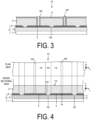
- FIG. 3 is a cross-sectional view illustrating another configuration of the semiconductor substrate according to the present embodiment.
- an edge growth 9G (corner portion) may be generated as depicted in FIG. 3 .
- the edge growth is generated when the function layer 9 includes an AlGaN layer, for example.
- the edge growth may have a width of 10 ⁇ m or more and a height of about 200 nm to about 300 nm, and becomes an obstacle in the post process.
- the edge growth 9G may be significantly reduced (for example, to 100 nm or less).
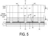
- FIG. 4 and FIG. 5 each include a plan view and a cross-sectional view illustrating another configuration of the semiconductor substrate according to the present embodiment.
- the semiconductor layer 8 in FIG. 4 has a configuration in which the semiconductor layers laterally grown in opposite directions from the two adjacent seed portions 3S meet each other near the center 5C of the mask portion and are integrated with each other.
- a hollow portion 8C may be formed near the center 5C of the mask portion, which is a meeting point, by appropriately setting the film formation conditions of the ELO semiconductor layer 8, the width of the mask portions 5, and the like.
- the shape of the hollow portion 8C is a shape that becomes wider on the mask portion 5 side (for example, a spindle shape or a drop shape in a cross-sectional view).
- the semiconductor layer 8 includes a portion (non-effective portion NS) overlapping the hollow portion 8C in a plan view. That is, the semiconductor layer 8 includes the effective portion YS and the non-effective portion NS adjacent to the effective portion YS.
- the surface of the semiconductor layer 8 may have a depression 8D at a portion corresponding to an upper portion of the hollow portion 8C.
- the depression 8D also has an effect of alleviating the internal stress of the semiconductor layer 8.
- the semiconductor substrate 10 in FIG. 2 includes the function layer 9 on the semiconductor layer 8.
- the function layer 9 includes, for example, at least one selected from the group consisting of a GaN-based n-type semiconductor layer, a GaN-based non-doped semiconductor layer, a GaN-based p-type semiconductor layer, an electrically conductive layer, and an insulation layer.
- the GaN-based semiconductor layer of the function layer 9 may be formed by any film formation method.
- the function layer 9 may be a compound semiconductor layer (compound semiconductor part).
- the compound semiconductor layer may be a nitride semiconductor layer (nitride semiconductor part).
- the nitride semiconductor layer may include a p-type layer and an active layer (for example, a light emitting layer), or may include an n-type layer, an active layer, and a p-type layer.
- the function layer 9 may constitute a semiconductor device (for example, an LED or a laser) together with the semiconductor layer 8, but is not limited thereto.
- a semiconductor device for example, an LED or a laser
- only a GaN-based n-type semiconductor layer may be provided.
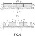
- FIG. 6 is a cross-sectional view illustrating an element separation step according to the present embodiment.
- FIG. 7 is a plan view illustrating the element separation step according to the present embodiment. As illustrated in FIG. 6 , a region AK overlapping the opening portion KS in a plan view in the semiconductor substrate 10 is removed by gas phase etching until the underlying layer 4 is reached.
- each of the underlying layer 4, mask layer 6, semiconductor layer 8, and function layer 9 is a target to be removed, and the underlying layer 4 and mask portion 5 are exposed in a trench TR (element separation trench) formed after the removal.
- the opening width of the trench TR is desirably larger than the width of the opening portion KS of the mask layer.
- An element portion DS may be separated in the semiconductor substrate 10 by the element separation step. At this stage, the element portion DS is bonded to the mask portion 5 of the template substrate by van der Waals bonding, and is part of the semiconductor substrate 10.
- the trench TR may be formed in a lattice shape (lattice pattern) in a plan view.
- a region surrounded by adjacent lateral trenches (extending in the X direction) and adjacent longitudinal trenches (extending in a Y direction) may include one element portion DS.
- the gas phase etching is implemented by a general photolithography method. After completion of the etching, the photoresist having served as the mask for the gas phase etching needs to be removed. When organic cleaning using weak ultrasonic waves is carried out, the element portion DS is unlikely to be peeled off from the mask portion 5.
- FIG. 8 is a cross-sectional view illustrating another example of the element separation step.
- a region overlapping the opening portion KS and a region overlapping the gap portion GP in a plan view in the semiconductor substrate 10 may be removed by gas phase etching until the underlying layer 4 is reached.
- the meandering of the semiconductor layer 8 in a second direction (the longitudinal direction of the opening portion KS, the Y direction) is eliminated, and the element portion DS having a uniform shape may be obtained.
- FIG. 9 is a cross-sectional view illustrating another example of the element separation step. As illustrated in FIG. 9 , a region overlapping the opening portion KS and a region overlapping a center portion of the mask portion 5 (non-effective portion NS) in a plan view in the semiconductor substrate 10 may be removed by gas phase etching until the underlying layer 4 is reached.
- FIG. 10 is a cross-sectional view illustrating an element peeling step. Since the semiconductor layer 8 and the mask portion 5 are bonded to each other by van der Waals force (weak force), by pulling up the function layer 9 with attractive force (adhesive force, suction force, electrostatic force, or the like) of a stamp device ST or the like, the element portion DS may be easily peeled off from the template substrate to obtain the semiconductor device 20, as illustrated in FIG. 10 . Direct peeling from the mask portion 5 can be carried out using a viscoelastic elastomer stamp, an electrostatic adhesion stamp, or the like, which brings a large advantage in terms of cost, throughput, and the like.
- the electrostatic adhesion stamp or the like is brought into contact with the semiconductor layer 8, for example, vibrations by ultrasonic waves may be applied. With vibrations or the like, the semiconductor layer 8 may be more easily peeled off from the mask portion 5.
- FIG. 11 is a cross-sectional view illustrating another example of the element peeling step.
- the element portion DS may be mechanically peeled off from the template substrate 7 with a tape TP or the like.
- the semiconductor device 20 having a large size may be formed.
- This peeling method has an advantage in that the element separation step may be omitted when the semiconductor layer 8 is of a separation type (when an edge face is present on the mask portion).
- the semiconductor layer 8 is of an integrated type (when an edge face is not present on the mask portion), there is an advantage that the element peeling is easy to carry out because only a dug portion for inflow of an etchant is required to be formed (down to the underlying layer).
- the element portion DS peeled off from the template substrate 7 functions as the semiconductor device 20.
- the semiconductor device 20 include a light-emitting diode (LED), a semiconductor laser, a Schottky diode, a photodiode, and a transistor (including a power transistor and a high electron mobility transistor).
- FIG. 12 is a schematic view illustrating a configuration of an electronic device according to the present embodiment.
- An electronic device 30 in FIG. 12 includes the semiconductor device 20 including the semiconductor layer 8 and the function layer 9, a drive substrate 23, on which the semiconductor device 20 is mounted, and a control circuit 25 configured to control the drive substrate 23.
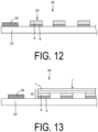
- FIG. 13 is a schematic view illustrating another configuration of the electronic device according to the present embodiment.
- the electronic device 30 in FIG. 13 includes the semiconductor substrate 10 including the semiconductor layer 8 and the function layer 9, the drive substrate 23, on which the semiconductor substrate 10 is mounted, and the control circuit 25 configured to control the drive substrate 23.
- the main substrate 1 may be a light-transmissive substrate (for example, a sapphire substrate).
- Examples of the electronic device include a display device, a laser emitting device (including a Fabry-Perot type and a surface emitting type), a measurement device, an illumination device, a communication apparatus, an information processing apparatus, and a power control device.
- a void may be generated in the back surface of the ELO semiconductor layer 8.
- This void becomes a cause of a surface defect of the ELO semiconductor layer 8 (for example, a start point of a defect when stress is applied to the semiconductor layer 8), and brings about degradation in characteristics and a decrease in the reliability of the device formed on the ELO semiconductor layer 8.
- the surface morphology of the mask portion 5 was improved, and consequently, the voids in the back surface of the ELO semiconductor layer 8 and the adhesion with the mask portion 5 were successfully reduced.
- the lateral film-formation rate is increased to quickly cover the mask portion 5 with the lateral growth film (ELO semiconductor layer 8). This is because, in the MOCVD, when the lateral film-formation rate is low, the mask portion 5 is exposed to hydrogen and nitrogen at a high temperature for a long time, and evaporation and decomposition of the mask portion 5 proceed, which may bring about deterioration in the surface morphology, generation of pin holes, generation of pits, and the like.
- a method for increasing the lateral film-formation rate is as follows. First, a longitudinal growth layer that grows in a c-axis direction is formed on the seed portion exposed from the opening portion KS of the mask layer 6, and then a lateral growth layer that grows in the a-axis direction is formed thereon.
- the thickness of the longitudinal growth layer to be 10 ⁇ m or less, preferably 5 ⁇ m or less, and more preferably 3 ⁇ m or less, the thickness of the lateral growth layer may be suppressed to be thin and the lateral film-formation rate may be increased.
- FIG. 14 is a cross-sectional view illustrating an example of a lateral growth of a semiconductor layer.
- an initial growth layer SL is formed on the seed portion 3S overlapping the opening portion KS, and then the semiconductor layer 8 is desirably grown laterally from the initial growth layer SL.
- the initial growth layer SL serves as a start point of the lateral growth of the semiconductor layer 8.
- the film formation of the initial growth layer SL is preferably stopped at a timing immediately before an edge of the initial growth layer SL rides on the upper surface of the mask portion 5 (at a stage of being in contact with the upper end of a side surface of the mask portion 5) or immediately after the edge of the initial growth layer SL rides on the upper surface of the mask portion 5 (that is, at this timing, the ELO film formation condition is switched from the c-axis direction film-formation condition to the a-axis direction film-formation condition).
- the initial growth layer SL may be formed to have a thickness of 50 nm to 5.0 ⁇ m (for example, 80 nm to 2 ⁇ m). The thickness of the initial growth layer SL may be equal to or less than 500 nm.
- the number of non-threading dislocations inside the effective portion YS may be increased (the threading dislocation density on the surface of the effective portion YS may be lowered).
- the distribution of the impurity concentration (for example, silicon or oxygen) inside the effective portion YS may be controlled.
- the semiconductor layer 8 may be controlled to grow in the Z direction (c-axis direction) or in the X direction (a-axis direction) by appropriately controlling the conditions during the film formation of the semiconductor layer 8.
- the ratio of a size W1 in the X direction (first direction) to a thickness d1 (W1/d1) may be set to 2.0 or more, for example.
- Using the technique of FIG. 14 makes it possible to set W11d1 to 1.5 or more, 2.0 or more, 4.0 or more, 5.0 or more, 7.0 or more, or 10.0 or more. It has been found that the dividing step as illustrated in FIG. 7 is facilitated by setting W11d1 to 1.5 or more. The internal stress of the semiconductor layer 8 is reduced and the substrate warp is reduced.
- Using the technique of FIG. 14 makes it possible to set the ratio of the size WL in the X direction of the semiconductor layer 8 to a width WK of the opening portion KS (WL/WK) to 3.5 or more, 5.0 or more, 6.0 or more, 8.0 or more, 10 or more, 15 or more, 20 or more, 30 or more, or 50 or more, and makes it possible to raise the ratio of the effective portion.
- the semiconductor layer 8 depicted in FIG. 14 may be a nitride semiconductor crystal (for example, a GaN crystal, an AlGaN crystal, an InGaN crystal, or an InAlGaN crystal).
- the non-threading dislocation is a dislocation observed by CL in a cross section taken along a plane parallel to the c-axis (a plane parallel to the thickness direction), and is mainly a basal plane (c-plane) dislocation.
- the plane parallel to the c-axis may be a plane parallel to the (1-100) plane (a plane whose normal line extends in the Y direction) or may be a plane parallel to the (11-20) plane (a plane whose normal line extends in the X direction).
- the non-threading dislocation density in the effective portion YS of the semiconductor layer 8 is higher than the threading dislocation density in the effective portion YS.
- the effective portion YS of the semiconductor layer 8 may be expressed as a GaN-based crystal body (GaN-based layer) in which the non-threading dislocation density is larger than the threading dislocation density.
- the non-threading dislocation density may be 10 times or more, for example, 20 times or more the threading dislocation density.
- the threading dislocation density may be, for example, 5 ⁇ 10 6 [pieces/cm 2 ] or less.
- the width (length in the X direction) of the effective portion (GaN-based crystal body) may be, for example, 10 ⁇ m or more.
- the effective portion may have a long shape in which the size in the Y direction (m-axis direction) is larger than the size in the X direction (a-axis direction).
- the non-threading dislocation density in a cross section taken along a plane parallel to the (11-20) plane may be larger than the non-threading dislocation density in a cross section taken along a plane parallel to the (1-100) plane.
- the concentration of impurities may be low, as compared with one end portion corresponding to the growth initial stage, at the other end portion corresponding to the growth termination stage in the X direction.
- the quality (thickness uniformity, film quality, and the like) of the mask portion 5 is affected by the surface flatness, crystallinity, and material of the underlying layer on which the mask portion 5 is formed.
- a reaction between the mask portion 5 and the underlying layer proceeds from the defective portion, thus the quality of the mask portion 5 is deteriorated.
- a reaction between the mask portion 5 and the ELO semiconductor layer 8 formed on the mask portion 5 is accelerated, and a void may be generated in the back surface of the ELO semiconductor (the boundary surface with the mask portion 5).
- the void is likely to be formed in a portion close to the center (a portion where the time until film formation is implemented is long).
- a film-forming temperature of the ELO semiconductor layer 8 is preferably 1150°C or less rather than a high temperature exceeding 1200°C.
- the ELO semiconductor layer 8 may be formed even at a low temperature below 1000°C, which is more preferable from the viewpoint of reducing the interaction. It has been found that in such low-temperature film formation, when trimethyl gallium (TMG) is used as a gallium raw material, the raw material is not sufficiently decomposed, and gallium atoms and carbon atoms are simultaneously taken into the ELO semiconductor layer 8 in larger quantities than usual.
- TMG trimethyl gallium
- the reason for this may be as follows: in the ELO method, since the film formation in the a-axis direction is fast and the film formation in the c-axis direction is slow, the above atoms are taken in during the c-plane film formation in large quantities.
- the carbon taken into the ELO semiconductor film reduces the reaction with the mask portion 5, reduces the interaction with the mask portion 5, and does not cause adhesion with the mask portion or the like 5.
- the supply amount of ammonia is reduced and the film formation is performed at a substantially low V/III ( ⁇ 1000), thereby making it possible to take the carbon elements in the raw material or a chamber atmosphere into the ELO semiconductor layer 8 and reduce the reaction with the mask portion 5.
- the semiconductor layer 8 contains carbon.
- triethylgallium (TEG) is preferably used as a gallium raw material gas. Since an organic raw material is efficiently decomposed at a low temperature with TEG as compared with TMG, the lateral film-formation rate may be increased.
- An InGaN layer may be formed as the ELO semiconductor layer 8.
- the lateral film formation of the InGaN layer is carried out at a low temperature below 1000°C, for example. This is because the vapor pressure of indium increases at a high temperature and indium is not effectively taken into the film.
- the film-forming temperature is low, an effect is exhibited in which the interaction between the mask portion 5 and the InGaN layer is reduced.
- the InGaN layer has an effect of exhibiting lower reactivity with the mask portion 5 than the GaN layer.
- indium is taken into the InGaN layer at an In composition level of 1% or more, the reactivity with the mask portion 5 is further lowered, which is desirable.
- TAG triethylgallium
- line defects in the surface (surface layer) of the ELO semiconductor layer 8 may be reduced.
- An m-plane of the ELO semiconductor layer 8 is vulnerable to stress, and therefore defects are likely to be generated.
- the line defects are assumed to have been generated due to a crystal slip along the m-plane.
- a dislocation extending in the m-axis direction (assumed to be a mixed dislocation in which an edge dislocation and a screw dislocation are combined) may be observed as a line defect.
- such a case is acceptable when the line defect disappears (is not observed) in a cross section (parallel to the c-plane) cut at a surface layer rather than this specific cross section.
- the adhesion between the ELO semiconductor layer 8 and the mask portion 5 is reduced.
- the material and thickness of the mask portion 5 are optimized, and the film density of the mask portion 5 is increased.
- the film density of the mask portion 5 is low, the evaporation of the film is early or the etching rate is high with respect to the film formation at a high temperature in a hydrogen atmosphere in the MOCVD device.
- the mask portion 5 such as that described above is covered with the laterally growing ELO semiconductor layer 8, the mask portion 5 and the ELO semiconductor layer 8 adhere to each other. The reason for this is assumed to be as follows: a reaction layer in which the mask portion 5 and the ELO semiconductor layer 8 are mixed is generated and the ELO semiconductor layer 8 is fixed to the mask portion 5.
- an intermediate layer (a layer in which the mask portion 5 and the semiconductor layer 8 react with each other or are mixed with each other) is formed on the back surface of the ELO semiconductor layer 8.
- This intermediate layer adheresion layer
- This intermediate layer is not removed even when the mask portion 5 is removed using an etchant such as hydrofluoric acid, but remains on the back surface of the ELO semiconductor layer 8. Because of this, when the intermediate layer is formed, the surface morphology of the back surface of the ELO semiconductor layer 8 after being peeled from the template substrate 7 is deteriorated.
- the influence of the adhesion is small when an arithmetic mean surface roughness Ra measured with an atomic force microscope (AFM) is less than or equal to 10 nm, and preferably about 1 nm.
- the influence of the adhesion was large when Ra was about 13 nm.
- a single-layer film made of any one of a titanium nitride film (TiN or the like), a silicon nitride film (SiN or the like), a silicon oxynitride film (SiON) and a high melting point metal film, or a multi-layer film made of two or more of the aforementioned may be cited.
- the mask portion 5 may be a silicon nitride film or a silicon oxynitride film.
- the silicon oxide film is decomposed and evaporated in a small amount during the formation of the ELO semiconductor layer 8 and may be taken into the ELO semiconductor layer 8, but the silicon nitride film and the silicon oxynitride film have an advantage in terms of hardly decomposing and evaporating at a high temperature. Even when a general silicon oxide film is used for the mask layer in the ELO method, the interaction between the mask portion 5 and the ELO semiconductor layer 8 may be effectively reduced by optimizing the film formation conditions of the mask layer and the ELO semiconductor layer 8.
- the mask layer may be a single-layer film of a silicon nitride film or a silicon oxynitride film, a multi-layer film in which a silicon oxide film and a silicon nitride film are formed in that order on the underlying layer, a multi-layer film in which a silicon nitride film and a silicon oxide film are formed in that order on the underlying layer, or a multi-layer film in which a silicon nitride film, a silicon oxide film, and a silicon nitride film are formed in that order on the underlying layer.
- An abnormal portion such as a pinhole in the mask portion 5 may be eliminated by performing organic cleaning or the like after film formation and introducing the film again into a film forming device to form the same type of film.
- a high-quality mask layer may be formed by using a general silicon oxide film and using the above-described mask reformation method.
- FIG. 15 to FIG. 18 each include a plan view and a schematic view illustrating evaluation of the present semiconductor substrate (a configuration in which the ELO semiconductor layer has an edge face on the mask).
- the back surface of the semiconductor layer 8 (a boundary surface 8R with the mask portion) may be evaluated in a state of being a boundary surface in contact with the mask portion 5, or the semiconductor layer 8 is peeled from the mask portion 5 and the peeled surface may also be evaluated.
- the semiconductor layer 8 may be peeled by removing the mask portion 5 by wet etching or the like (note that when the semiconductor layer 8 is of an integrated type, digging may be performed in advance until the underlying layer 4 is reached).
- an upper surface 8F of the effective portion YS included at least one low-level defective region AL having a size of 10 ⁇ m in the first direction X (a-axis direction) along the width direction of the opening portion KS and 10 ⁇ m in the second direction Y (m-axis direction) orthogonal to the first direction, and no line defect (line defect oblique with respect to the first direction X assumed to have been brought about by an m-plane slip) was measured in the low-level defective region AL (see FIG. 15 , evaluation criterion 1).
- the upper surface of the effective portion YS included the plurality of low-level defective regions AL arranged in the first direction X and the plurality of low-level defective regions AL arranged in the second direction Y (see FIG. 15 , evaluation criterion 2).
- the size in the first direction of the effective portion YS was larger than the width of the opening portion KS (see FIG. 15 , evaluation criterion 3).
- the effective portion YS included, at the boundary surface 8R with the mask portion 5, a first region A1 having a size of 10 ⁇ m in the first direction X and 10 ⁇ m in the second direction Y, and a second region A2 having the same size as that of the first region A1, located closer to the center side of the mask portion 5 than the first region A1, and having an interval PT with the center 5C of the mask portion 5, the interval PT being 30% or less the width of the mask portion 5. Then, the effective portion YS was peeled from the mask portion 5 and the first region A1 and the second region A2 were observed with the AFM.
- the number of recessed portions having a major axis of 0.1 [ ⁇ m] or more in the first region A1 was equal to or less than the number of recessed portions having a major axis of 0.1 ⁇ m or more in the second region A2 (see FIG. 16 , evaluation criterion 4).
- the major axis of the recessed portions present in the first region A1 was 1 ⁇ m or less (hereinafter, evaluation criterion 5).
- the number of voids having a major axis of 0.1 ⁇ m or more in the first region A1 was equal to or less than the number of voids having a major axis of 0.1 ⁇ m or more in the second region A2 (see FIG. 16 , evaluation criterion 6).
- the effective portion YS included, at the boundary surface 8R with the mask portion 5, a third region A3 having a size of 10 ⁇ m in the first direction X and 10 ⁇ m in the second direction Y, and a fourth region A4 having the same size as that of the third region A3 and located closer to the center side of the mask portion 5 than the third region A3. Then, the effective portion YS was peeled from the mask portion 5 and the first region A3 and the second region A4 were observed with the AFM. As a result, an adhesion area in the third region A3 was smaller than an adhesion area in the fourth region A4 (see FIG. 17 , evaluation criterion 7).
- the third region A3 was a non-adhesion region in which adhesion with the mask portion 5 was not substantially observed (hereinafter, evaluation criterion 8).
- the fourth region A4 was located at a position where the interval PT between the fourth region A4 and the center 5C of the mask portion was 30% or less the width of the mask portion 5.
- the effective portion YS included a first portion P1 and a second portion P2 farther from the opening portion KS than the first portion P1 and having an interval KT of 10 ⁇ m or more with the opening portion KS. Due to the surface roughness (Ra) of a peeled surface F1 when the first portion P1 was peeled from the mask portion 5 being defined as a first surface roughness, and the surface roughness (Ra) of a peeled surface F2 when the second portion P2 was peeled from the mask portion 5 being defined as a second surface roughness, the first surface roughness was equal to or less than the second surface roughness (see FIG. 18 , evaluation criterion 9).
- the arithmetic mean roughness (Ra) in a range of 5 ⁇ m ⁇ 5 ⁇ m of each peeled surface may be represented by the mean value of an unevenness state in the extracted section.
- the value of the ratio of the second surface roughness to the first surface roughness was 1.0 to 10 (evaluation criterion 10).
- the peeled surfaces (including F1 and F2) obtained when the effective portion YS was peeled from the mask portion 5 included a flat region having a size of 10 ⁇ m in the first direction and 10 ⁇ m in the second direction and having no recessed portion with a major axis of 0.1 ⁇ m or more (evaluation criterion 11).
- the second surface roughness was less than 10 nm (evaluation criterion 12).
- the first portion P1 was adjacent to the opening portion KS, and the interval PT between the second portion P2 and the center 5C of the mask portion was 30% or less the width of the mask portion 5 (evaluation criterion 13).
- the first recessed portion occupancy ratio was equal to or less than the second recessed portion occupancy ratio (evaluation criterion 14).
- the recessed portions are measured with the AFM in a range of 5 ⁇ m ⁇ 5 ⁇ m of each peeled surface, thereby making it possible to obtain the major axes, occupancy ratios, and the like.
- the impurity concentration in the peeled surface F1 of the first portion P1 was higher than the impurity concentration in the peeled surface F2 of the second portion P2 (evaluation criterion 15).
- the threading dislocation density in the upper surface 8R of the effective portion YS was 5 ⁇ 10 6 [pieces/cm 2 ] or less (evaluation criterion 16).
- the crystallinity of the ELO semiconductor layer 8 laterally grown on the mask 5 from the opening portion KS of the mask 5 is significantly high.
- the semiconductor substrate 10 by reducing the interaction between the mask portion 5 and the semiconductor layer 8, voids and adhesion generated in the back surface of the semiconductor layer 8 are decreased and the stress from the main substrate 1 is effectively alleviated. This indicates that the defect generated in the effective portion YS does not penetrate to the surface of the semiconductor layer 8 but is confined therein.
- FIG. 19 to FIG. 22 each include a plan view and a schematic view illustrating evaluation of a semiconductor substrate in another configuration (an integrated type in which an ELO semiconductor layer does not have an edge face on a mask). Also, in this case, it was found that the evaluation criteria 1 to 16 mentioned above were satisfied.
- FIG. 23 is a cathode luminescence (CL) image obtained by taking the ELO semiconductor layer 8 in the semiconductor substrate 10 (the main substrate is a silicon substrate) as an imaging subject. Neither a dark spot nor a dark line is observed in the effective portion YS. Only in the non-effective portion NS, approximately 10 19 /cm 2 threading dislocations due to a difference in lattice constant between the silicon substrate and GaN are present.
- CL cathode luminescence
- FIG. 24 is a cathode luminescence (CL) image obtained by taking the ELO semiconductor layer 8 in the semiconductor substrate 10 (the main substrate is a sapphire substrate) as an imaging subject. Since the ELO semiconductor layer 8 is mechanically peeled from the template substrate, the non-effective portion NS is slightly damaged and the peeled surface is not flat, thus the CL image is slightly disordered. However, a dark spot, a dark line, or the like, which is a threading dislocation, is not seen in the effective portion YS, or a low dislocation density is achieved.
- CL cathode luminescence
- FIG. 25 is a CL image obtained by taking the ELO semiconductor layer back surface (peeled surface) in the semiconductor substrate 10 as an imaging subject.
- the CL image shows that neither a void nor adhesion is observed in the effective portion YS.
- FIG. 26 is a CL image of a surface of a GaN layer of a reference example.
- sapphire is used as the main substrate, and a GaN layer is film-formed by the ELO method.
- Both dark spots (10 18 to 10 19 /cm 2 ) and dark lines, which are high-density threading dislocations, are present above the opening portion. Above the mask portion as well, dark spots and dark lines are observed although the density is lower than that above the opening portion.
- FIG. 27 is a CL image of a surface of a GaN layer of a reference example.
- silicon is used as the main substrate, and a GaN layer is film-formed by the ELO method. Approximately 10 19 /cm 2 dark spots are observed above the opening portion, and dark lines are observed also above the mask portion.
- FIG. 28 is a CL image of a back surface of a GaN layer of a reference example.
- silicon is used as the main substrate, and a GaN layer is film-formed by the ELO method. A large number of voids are seen at end portions above the mask portion.
- FIG. 29 is a light microscope image obtained by taking a back surface (peeled surface) of a GaN layer having been film-formed by the ELO method in a reference example as an imaging subject. Adhesion NL (reaction layer) between the mask portion and the GaN layer can be seen.
- a GaN layer is mechanically peeled from the mask portion (for example, by using a diamond pen)
- the GaN layer and the mask portion are peeled together from the template substrate as depicted in a peeling region NA in FIG. 30 .
- the reference examples indicate that the use of only the ELO method does not make it possible to eliminate voids and adhesion and significantly decrease surface defects above the mask portion.
- dark lines linear defects
- their reduction is of great significance because when they occur, they affect a wide range.
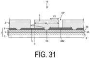
- FIG. 31 is a cross-sectional view illustrating a configuration of a semiconductor substrate of Example 1.
- a silicon substrate having a (111) plane was used as the main substrate 1.
- the buffer layer 2 of the underlying layer 4 was an AlN layer (for example, 30 nm).
- the seed layer 3 of the underlying layer 4 was a graded layer in which an Al 0.6 Ga 0.4 N layer (for example, 300 nm) as a first layer and a GaN layer (for example, 1 to 2 ⁇ m) as a second layer were formed in that order.
- a laminate body in which a silicon oxide film (SiO 2 ) and a silicon nitride film (SiN) were formed in that order was used.
- the silicon oxide film has a thickness of 0.3 ⁇ m, for example, and the silicon nitride film has a thickness of 70 nm, for example.
- Each of the silicon oxide film and the silicon nitride film was film-formed by a plasma chemical vapor deposition (CVD) method.
- the semiconductor layer 8 was a GaN layer, and ELO film formation was performed using an MOCVD device. First, the ELO semiconductor layer 8 was selectively grown on the surface of the seed layer 3 (the GaN layer of the second layer) exposed to the opening portion KS, and subsequently laterally grown on the mask portion 5. At this time, the growth was stopped before the semiconductor layers laterally grown from both sides of the mask portion 5 met each other. The width of the gap GP at this time was 2 ⁇ m.
- a width WM of the mask portion 5 was 50 ⁇ m
- the width of the opening portion KS was 5 ⁇ m
- a lateral width WL of the ELO semiconductor layer 8 was 53 ⁇ m
- the width (size in the X direction) of the effective portion YS was 24 ⁇ m.
- the layer thickness of the ELO semiconductor layer 8 was 5 ⁇ m
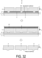
- the peeling of the semiconductor layer 8 during the evaluation of the back surface of the semiconductor layer 8 may be performed as follows.
- the semiconductor substrate 10 having been subjected to the element separation step (see FIGs. 8 and 9 ) is immersed in an etchant of hydrofluoric acid for about 10 to 60 minutes, thus the mask layer 6 is dissolved in the etchant and the semiconductor layer 8 may be peeled from the template substrate 7.
- the semiconductor substrate 10 may be immersed in an etchant of hydrofluoric acid to dissolve the mask layer 6, then an adhesive tape (for example, an adhesive dicing tape used when dicing a semiconductor wafer) may be attached to the surface of the semiconductor layer 8, and the temperature of the semiconductor substrate 10 with the adhesive tape attached thereto as is may be lowered to a low temperature using a Peltier element.
- an adhesive tape for example, an adhesive dicing tape used when dicing a semiconductor wafer
- the adhesive tape generally having a larger thermal expansion coefficient than the semiconductor contracts considerably and applies stress to the semiconductor layer 8.
- the stress from the adhesive tape is effectively applied to a bonding portion with the template substrate 7, and consequently the bonding portion may be mechanically cleaved or broken. In other words, dry etching is not needed for the removal of the bonding portion.
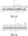
- FIG. 33 is a cross-sectional view illustrating a configuration of a semiconductor substrate of Example 2.
- Example 2 an integrated type is employed in which the ELO semiconductor layer 8 does not have an edge face on the mask portion 5.
- the width of the mask portion 5 is 50 ⁇ m, and the width of the opening portion KS is 5 ⁇ m.
- the height of the hollow portion 8C is preferably 1 ⁇ m or more.
- the width of the bottom surface of the hollow portion 8C is also preferably 1 ⁇ m or more, and more preferably 2 ⁇ m or more.
- FIG. 34 is a cross-sectional view illustrating a configuration of a semiconductor substrate of Example 3.
- the width of the opening portion KS was 700 nm being 1 ⁇ m or less, and the width of the mask portion 5 was 100 ⁇ m.
- the configuration of Example 3 is suitable for a high-power laser semiconductor element (with a ridge width of about 40 ⁇ m) or the like.
- FIG. 34 illustrates a structure in which the semiconductor layer 8 has an edge face on the mask portion 5, but the semiconductor layer 8 may be of an integrated type having no edge on the mask portion 5.
- FIG. 35 is a cross-sectional view illustrating a configuration of Example 4.
- the function layer 9 constituting an LED is film-formed on the semiconductor layer 8.
- the semiconductor layer 8 is an n-type layer doped with, for example, silicon.
- the function layer 9 includes an active layer 34, an electron blocking layer 35, and a GaN-based p-type semiconductor layer 36 in that order from the bottom layer side.
- the active layer 34 is a multi-quantum well (MQW), and includes an InGaN layer and a GaN layer.
- the electron blocking layer 35 is, for example, an AlGaN layer.
- the GaN-based p-type semiconductor layer 36 is, for example, a GaN layer.
- An anode 38 is formed to be in contact with the GaN-based p-type semiconductor layer 36, and a cathode 39 is formed to be in contact with the semiconductor layer 8.
- Voids in the back surface of the semiconductor layer cause surface defects (line defects) and degrade the characteristics of the semiconductor device.
- the semiconductor device is a light emitting element
- the voids in the back surface of the semiconductor layer reduce the in-plane uniformity of the emitted light.
- the element portion (light emitting element portion) DS is formed on the ELO semiconductor layer 8, and the semiconductor device 20 as a light emitting element can be obtained by peeling off the element portion DS, thus the above problems may be improved. Specifically, no defect was observed in the light emitting region of the semiconductor device 20.
- FIG. 36 is a cross-sectional view illustrating an application example of Example 4.
- a red micro LED 20R, a green micro LED 20G, and a blue micro LED 20B may be obtained, and a micro LED display 30D (electronic device) may be constituted by mounting these LEDs on the drive substrate (TFT substrate) 23.
- the red micro LED 20R, the green micro LED 20G, and the blue micro LED 20B are mounted on a plurality of pixel circuits 27 of the drive substrate 23 via a conductive resin 24 (for example, an anisotropic conductive resin) or the like, and then the control circuit 25, a driver circuit 29, and the like are mounted on the drive substrate 23.
- the drive substrate 23 may include part of the driver circuit 29.
- FIG. 37 is a cross-sectional view illustrating a configuration of Example 5.
- the function layer 9 constituting a semiconductor laser is film-formed on the semiconductor layer 8.
- the function layer 9 includes an n-type light cladding layer 41, an n-type light guide layer 42, an active layer 43, an electron blocking layer 44, a p-type light guide layer 45, a p-type light cladding layer 46, and a GaN-based p-type semiconductor layer 47 in that order from the bottom layer side.
- an InGaN layer may be used for each of the guide layers 42 and 45.
- a GaN layer or AlGaN layer may be used for each of the cladding layers 41 and 46.
- An anode 48 is formed to be in contact with the GaN-based p-type semiconductor layer 47.
- Example 5 as depicted in FIG. 37 , after the element portion DS is peeled off, a cathode 49 is formed on the back surface of the semiconductor layer 8. Accordingly, the quality of the back surface of the semiconductor layer 8 affects the device characteristics.
- FIG. 38 is a cross-sectional view illustrating a configuration of Example 6.
- FIG. 39 is a cross-sectional view illustrating another configuration of Example 6.
- a sapphire substrate having an uneven surface is used for the main substrate 1.
- the underlying layer 4 includes the buffer layer 2 and the seed layer 3.
- the semiconductor layer 8 may be of a type having an edge face on the mask 5 ( FIG. 38 ), or may be of an integrated type having no edge face on the mask ( FIG. 39 ).
- a GaN layer having a (20-21) plane may be film-formed as the underlying layer 4 on the main substrate 1.
- the ELO semiconductor layer 8 becomes the (20-21) plane, which is a crystal principal plane, in the underlying layer 4, and the ELO semiconductor layer 8 of a semi-polar plane may be obtained.
- a function layer for a laser or an LED on the semi-polar plane an advantage is obtained in that the piezoelectric field is weak and the probability of recombination of electrons and holes is increased in the active layer.
- a GaN layer having a (11-22) plane may be film-formed as the underlying layer 4 on the main substrate 1 by using a sapphire substrate having an uneven surface.
- a method for manufacturing the semiconductor substrate 10 includes at least a step of forming the semiconductor layer 8 on the template substrate 7 by using the ELO method.
- a step of forming the underlying layer 4 and the mask layer 6 on the main substrate 1 may be included.
- the semiconductor substrate 10 may be manufactured by, for example, a semiconductor substrate manufacturing apparatus illustrated in FIG. 40 .
- the semiconductor substrate manufacturing apparatus 70 at least includes a semiconductor layer forming unit 71 configured to perform the step of forming the semiconductor layer 8 on the template substrate 7 by using the ELO method, and a controller 72 configured to control the semiconductor layer forming unit 71.
- the semiconductor layer forming unit 71 may include an MOCVD device, and the controller 72 may include a processor and a memory.
- the controller 72 may be configured to control the semiconductor layer forming unit 71 by executing a program stored in a built-in memory, a communicable communication apparatus, or an accessible network, for example, and the above program, a recording medium storing the above program therein, and the like are also included in the present embodiment.
- the semiconductor substrate manufacturing apparatus 70 may include a template substrate forming unit configured to perform a step of forming the underlying layer 4 and the mask layer 6 on the main substrate 1, and a function layer forming unit configured to perform a step of forming the function layer 9 on the semiconductor layer 8.
- a semiconductor device manufacturing apparatus configured to perform an element peeling step may also be constructed.
- the semiconductor device manufacturing apparatus may perform an element separation step.
- the semiconductor device manufacturing apparatus may include the semiconductor substrate manufacturing apparatus 70.
Landscapes
- Chemical & Material Sciences (AREA)
- Metallurgy (AREA)
- Organic Chemistry (AREA)
- Materials Engineering (AREA)
- Engineering & Computer Science (AREA)
- General Chemical & Material Sciences (AREA)
- Chemical Kinetics & Catalysis (AREA)
- Crystallography & Structural Chemistry (AREA)
- Inorganic Chemistry (AREA)
- Mechanical Engineering (AREA)
- Physics & Mathematics (AREA)
- General Physics & Mathematics (AREA)
- Condensed Matter Physics & Semiconductors (AREA)
- Optics & Photonics (AREA)
- Electromagnetism (AREA)
- Led Devices (AREA)
- Recrystallisation Techniques (AREA)
- Crystals, And After-Treatments Of Crystals (AREA)
- Encapsulation Of And Coatings For Semiconductor Or Solid State Devices (AREA)
- Structures Or Materials For Encapsulating Or Coating Semiconductor Devices Or Solid State Devices (AREA)
Abstract
Description
- The present invention relates to semiconductor substrates, semiconductor devices, and electronic devices.
- A semiconductor device using gallium nitride (GaN) generally has higher power conversion efficiency than a semiconductor device made of silicon (Si). Because of this, a semiconductor device using GaN has a smaller power loss than a semiconductor device made of Si, and thus an energy saving effect is expected. In order to manufacture semiconductor devices using GaN, research has been conducted on a technique for forming GaN-based semiconductor elements. For example, Patent Document 1 discloses a technique for forming a GaN-based semiconductor layer on a GaN-based substrate or a heterogeneous substrate (for example, a sapphire substrate) by using an epitaxial lateral overgrowth (ELO) method.
- Patent Document 1:
JP 2013-251304 A - A semiconductor substrate according to the present disclosure includes a main substrate having a lattice constant different from that of a GaN-based semiconductor, a mask layer located above the main substrate and including an opening portion and a mask portion, a seed portion overlapping the opening portion in a plan view, and a semiconductor layer including a GaN-based semiconductor and disposed on the seed portion and the mask portion. The semiconductor layer includes an effective portion located between the opening portion and a center of the mask portion in a plan view. An upper surface of the effective portion includes at least one low-level defective region with a size of 10 µm in a first direction along a width direction of the opening portion and 10 µm in a second direction orthogonal to the first direction. In the low-level defective region, a line defect is not measured by a CL method.
-
-
FIG. 1 includes a plan view and a cross-sectional view illustrating a configuration of a semiconductor substrate according to the present embodiment. -
FIG. 2 is a cross-sectional view illustrating another configuration of the semiconductor substrate according to the present embodiment. -
FIG. 3 is a cross-sectional view illustrating another configuration of the semiconductor substrate according to the present embodiment. -
FIG. 4 includes a plan view and a cross-sectional view illustrating another configuration of the semiconductor substrate according to the present embodiment. -
FIG. 5 includes a plan view and a cross-sectional view illustrating another configuration of the semiconductor substrate according to the present embodiment. -
FIG. 6 is a cross-sectional view illustrating an element separation step according to the present embodiment. -
FIG. 7 is a plan view illustrating the element separation step according to the present embodiment. -
FIG. 8 is a cross-sectional view illustrating another example of the element separation step. -
FIG. 9 is a cross-sectional view illustrating another example of the element separation step. -
FIG. 10 is a cross-sectional view illustrating an element peeling step. -
FIG. 11 is a cross-sectional view illustrating another example of the element peeling step. -
FIG. 12 is a schematic view illustrating a configuration of an electronic device according to the present embodiment. -
FIG. 13 is a schematic view illustrating another configuration of the electronic device according to the present embodiment. -
FIG. 14 is a cross-sectional view illustrating an example of a lateral growth of a semiconductor layer. -
FIG. 15 includes a plan view and a schematic view illustrating evaluation of the present semiconductor substrate (a configuration in which an ELO semiconductor layer has an edge face on a mask). -
FIG. 16 includes a plan view and a schematic view illustrating evaluation of the present semiconductor substrate (a configuration in which an ELO semiconductor layer has an edge face on a mask). -
FIG. 17 includes a plan view and a schematic view illustrating evaluation of the present semiconductor substrate (a configuration in which an ELO semiconductor layer has an edge face on a mask). -
FIG. 18 includes a plan view and a schematic view illustrating evaluation of the present semiconductor substrate (a configuration in which an ELO semiconductor layer has an edge face on a mask). -
FIG. 19 includes a plan view and a schematic view illustrating evaluation of an integrated-type semiconductor substrate in which an ELO semiconductor layer does not have an edge face on a mask. -
FIG. 20 includes a plan view and a schematic view illustrating evaluation of an integrated-type semiconductor substrate in which an ELO semiconductor layer does not have an edge face on a mask. -
FIG. 21 includes a plan view and a schematic view illustrating evaluation of an integrated-type semiconductor substrate in which an ELO semiconductor layer does not have an edge face on a mask. -
FIG. 22 includes a plan view and a schematic view illustrating evaluation of an integrated-type semiconductor substrate in which an ELO semiconductor layer does not have an edge face on a mask. -
FIG. 23 is a CL image obtained by taking anELO semiconductor layer 8 in a semiconductor substrate 10 (a main substrate is a silicon substrate) as an imaging subject. -
FIG. 24 is a CL image obtained by taking theELO semiconductor layer 8 in the semiconductor substrate 10 (the main substrate is a sapphire substrate) as an imaging subject. -
FIG. 25 is a CL image obtained by taking an ELO semiconductor layer back surface (peeled surface) in thesemiconductor substrate 10 as an imaging subject. -
FIG. 26 is a CL image of a surface of a GaN layer in a reference example. -
FIG. 27 is a CL image of a surface of a GaN layer in a reference example. -
FIG. 28 is a CL image of a surface of a GaN layer in a reference example. -
FIG. 29 is a CL image obtained by taking, as an imaging subject, a back surface (peeled surface) of a GaN layer film formed by an ELO method in a reference example. -
FIG. 30 is a CL image obtained by taking, as an imaging subject, a back surface (peeled surface) of a GaN layer film formed by the ELO method in a reference example. -
FIG. 31 is a cross-sectional view illustrating a configuration of a semiconductor substrate of Example 1. -
FIG. 32 is a cross-sectional view illustrating an example of peeling of a semiconductor layer in Example 1. -
FIG. 33 is a cross-sectional view illustrating a configuration of a semiconductor substrate of Example 2. -
FIG. 34 is a cross-sectional view illustrating a configuration of a semiconductor substrate of Example 3. -
FIG. 35 is a cross-sectional view illustrating a configuration of a semiconductor substrate of Example 4. -
FIG. 36 is a cross-sectional view illustrating an application example of Example 4. -
FIG. 37 is a cross-sectional view illustrating a configuration of Example 5. -
FIG. 38 is a cross-sectional view illustrating a configuration of Example 6. -
FIG. 39 is a cross-sectional view illustrating another configuration of Example 6. -
FIG. 40 is a block diagram illustrating a configuration example of a manufacturing apparatus of a semiconductor substrate. -
FIG. 1 includes a plan view and a cross-sectional view illustrating a configuration of a semiconductor substrate according to the present embodiment. As illustrated inFIG. 1 , asemiconductor substrate 10 according to the present embodiment (semiconductor wafer) includes a main substrate 1, anunderlying layer 4 formed on the main substrate 1 and including aseed portion 3S, amask layer 6 formed on theunderlying layer 4 and including an opening portion KS overlapping theseed portion 3S in a plan view and amask portion 5, and asemiconductor layer 8 disposed on theseed portion 3S and themask portion 5 and including a nitride semiconductor (for example, a GaN-based semiconductor). Theunderlying layer 4 may be referred to as anunderlying portion 4, themask layer 6 may be referred to as a mask 6 (mask pattern), and thesemiconductor layer 8 may be referred to as asemiconductor part 8. - The opening portion KS of the
mask layer 4 may have a tapered shape (a shape in which the width becomes narrower toward theunderlying layer 4 side). In this case, the width of the opening portion KS and the width of themask portion 5 may be expressed while taking the upper surface of the mask layer as a measurement subject. However, the aforementioned are not limited thereto. - A nitride semiconductor may be expressed, for example, by AlxGayInzN (0 ≤ x ≤ 1; 0 ≤ Y ≤ 1; 0 ≤ Z ≤ 1; X + Y + Z = 1). Specific examples may include a GaN-based semiconductor, aluminum nitride (AlN), indium aluminum nitride (InAlN), and indium nitride (InN). The GaN-based semiconductor is a semiconductor containing gallium atoms (Ga) and nitrogen atoms (N). Typical examples of the GaN-based semiconductor include GaN, AlGaN, AlGaInN, and InGaN. The
semiconductor layer 8 may be a doped type (for example, an n-type including a donor) or a non-doped type. The semiconductor substrate refers to a substrate including a nitride semiconductor (for example, a GaN-based semiconductor), and a material of the main substrate 1 may be a semiconductor or a non-semiconductor. The main substrate 1 and theunderlying layer 4 may be collectively referred to as a base substrate, and the main substrate 1, theunderlying layer 4, and themask layer 6 may be collectively referred to as atemplate substrate 7. - The
semiconductor layer 8 is formed by an epitaxial lateral overgrowth (ELO) method starting from theseed portion 3S exposed from the opening portion KS. Thus, thesemiconductor layer 8 may be referred to as theELO semiconductor layer 8. A thickness direction of thesemiconductor layer 8 is a Z direction (<0001> direction of a GaN-based crystal). The opening portion KS has a long shape, and its width direction is an X direction (<11-20> direction of the GaN-based crystal). -
FIG. 2 is a cross-sectional view illustrating another configuration of the semiconductor substrate according to the present embodiment. As illustrated inFIG. 2 , thesemiconductor substrate 10 may have a configuration in which the main substrate 1, theunderlying layer 4, themask layer 6, thesemiconductor layer 8, and afunction layer 9 are provided in that order. - In the
semiconductor substrate 10, a plurality of layers are layered on the main substrate, and a layering direction thereof may be defined as an "upward direction". Viewing thesemiconductor substrate 10 with a line of sight parallel to a normal direction of thesemiconductor substrate 10 may be referred to as a "plan view". - A heterogeneous substrate having a lattice constant different from that of a GaN-based semiconductor may be used for the main substrate 1. Examples of the heterogeneous substrate include a silicon (Si) substrate, a sapphire (Al2O3) substrate, a silicon carbide (SiC) substrate, and a ScAlMgO4 substrate. The plane orientation of the main substrate 1 is, for example, the (111) plane of the silicon substrate, the (0001) plane of the sapphire substrate, or the 6H-SiC (0001) plane of the SiC substrate. These are merely examples, and any substrate and any plane orientation may be used as long as the
semiconductor layer 8 can be grown by the ELO method. The main substrate may be a free-standing substrate (for example, a wafer cut out from a bulk crystal). - As the
underlying layer 4, a buffer layer 2 (for example, an AlN layer) and a seed layer 3 (for example, a GaN-based semiconductor) may be provided in that order from the main substrate side. Thebuffer layer 2 is a melt suppression layer that can suppress a situation in which the main substrate 1 and theseed layer 3 come into direct contact with each other and melt together. It also has an effect of enhancing the crystallinity of theseed layer 3. The AlN layer is formed using a MOCVD method, for example, to have a thickness of about 10 nm to about 5 µm. For example, when the main substrate 1 unlikely to melt together with theseed layer 3, which is a GaN-based semiconductor, is used, a configuration may be employed in which thebuffer layer 2 is not provided. When a silicon substrate or the like is used for the main substrate 1, the main substrate 1 and the GaN-based semiconductor serving as the seed layer melt together. Then, for example, by providing thebuffer layer 2 such as an AlN layer, the melting is suppressed. - For example, an AlGaN layer may be used for the
seed layer 3. Theseed layer 3 includes theseed portion 3S overlapping the opening portion KS of themask layer 6. As theseed layer 3, a graded layer in which the Al composition approaches GaN in a graded manner may be used. The graded layer is, for example, a laminate body in which an Al0.7Ga0.3N layer as a first layer and an Al0.3Ga0.7N layer as a second layer are provided in that order from the AlN layer side. In this case, the Ga composition ratio (0.7/2 = 0.35) in the second layer (Al : Ga : N = 0.3 : 0.7 : 1) is larger than the GA composition ratio (0.3/2 = 0.15) in the first layer (Al : Ga : N = 0.7 : 0.3 : 1). The graded layer may be easily formed by the MOCVD method and may be composed of three or more layers. By using the graded layer for theseed layer 3, stress from the main substrate 1 as the heterogeneous substrate may be alleviated. Theseed layer 3 may have a configuration including a GaN layer. In this case, theseed layer 3 may be a GaN single layer, or the uppermost layer of the graded layer as theseed layer 3 may be a GaN layer. Theunderlying layer 4 may be composed of only one of thebuffer layer 2 and theseed layer 3. Alternatively, a free-standing SiC substrate (for example, a single-crystal wafer cut out from a bulk crystal) may be used as the main substrate 1, and themask layer 6 may be formed on the SiC substrate to obtain the template substrate without forming the underlying layer. - The
mask portion 5 and the opening portion KS are formed in themask layer 6. The opening portion KS exposes theseed layer 3 and has a function of a growth start opening to start the growth of thesemiconductor layer 8. Themask portion 5 may have a function of a selective growth mask to cause thesemiconductor layer 8 to grow in the lateral direction. The opening portion KS is a portion where themask portion 5 in the mask layer 6 (mask pattern 6) is not present (no-formation portion), and need not be surrounded by themask portion 5. - As the
mask layer 6, an inorganic insulating film such as a silicon oxide (SiOx) film, a silicon nitride (SiNx) film, a silicon oxynitride film (SiON), a titanium nitride (TiNx) film or the like may be used. For example, a silicon oxide film having a thickness of about 50 nm to about 4 µm (for example, about 100 nm to about 2 µm) is formed on the entire surface of theunderlying layer 4 by sputtering, and a resist is applied onto the entire surface of the silicon oxide film. Thereafter, the resist is patterned by photolithography to form the resist having a stripe-shaped opening portion. Thereafter, part of the silicon oxide film is removed by a wet etchant such as hydrofluoric acid (HF), buffered hydrofluoric acid (BHF) or the like to form the opening portion KS, and the resist is removed by organic cleaning to form themask layer 6 having the opening portion KS and themask portion 5. The mask portion may be formed on the entire surface of the substrate by photolithography; thereafter, a resist may be applied and patterned, the resist in a region to be the opening portion KS may be removed, and then the opening portion KS may be formed using a dry etching method. - The opening portion KS has a long shape, and a plurality of opening portions KS is periodically arranged with a first period in an a-axis direction (first direction X) of the
ELO semiconductor layer 8. - The width of the opening portion KS is about 0.1 µm to 20 µm. As the width of the opening portion KS is smaller, the number of threading dislocations propagating from the opening portion KS to the
ELO semiconductor layer 8 is reduced. TheELO semiconductor layer 8 may be easily peeled in a post process. An area of an effective portion with few surface defects may be increased. - For the
mask layer 6, a laminate film including the above-described materials, for example, a laminate film including a silicon oxide film and a silicon nitride film may also be used. - As the semiconductor layer 8 (ELO semiconductor layer 8), a GaN-based semiconductor layer is formed by the ELO method. The
ELO semiconductor layer 8 may be made of GaN, and theseed portion 3S may contain GaN. For example, thetemplate substrate 7 including the main substrate 1, theunderlying layer 4, and themask layer 6 is introduced into an MOCVD device to film-form a GaN layer on thetemplate substrate 7. The following may be adopted as examples of the ELO film formation conditions: substrate temperature: 1120°C, growth pressure: 50 kPa, trimethylgallium (TMG): 22 sccm, NH3: 15 slm, and V/III = 6000 (ratio of group V raw material supply amount to group III raw material supply amount). - In the film formation of the
semiconductor layer 8, interaction between thesemiconductor layer 8 and themask portion 5 is preferably reduced, and a state in which thesemiconductor layer 8 and themask portion 5 are in contact with each other by van der Waals force is preferably maintained. That is, thesemiconductor layer 8 and themask portion 5 are in contact with each other mainly by van der Waals force. - The adjacent ELO semiconductor layers 8 respectively grown from the adjacent opening portions KS may meet each other, or may form a gap near the center of the
mask portion 5 by not meeting each other. When meeting each other, the entire surface of the substrate may form a flat surface. When not meeting each other, stress (compressive stress or tensile stress) generated when the main substrate 1 mainly composed of a material different from the nitride semiconductor is used may be more effectively alleviated by the gap, thus the occurrence of defects, cracks, and the like may be effectively suppressed. - The
semiconductor layer 8 includes an effective portion YS (a portion to constitute an element portion in the post process) located between the opening portion KS and acenter 5C of the mask portion in a plan view. A portion of thesemiconductor layer 8 located over theseed portion 3S (a portion having many threading dislocations) is a non-effective portion NS. That is, thesemiconductor layer 8 includes the effective portion YS having a relatively small number of threading dislocations and the non-effective portion NS having a relatively large number of threading dislocations. The non-effective portion NS is a dislocation successive portion and has more threading dislocations than the effective portion YS (dislocation non-successive portion), but may be used as part of the device. For example, when thefunction layer 9 includes an active layer, a portion (light emitting portion) of the active layer where electrons and positive holes are combined may be provided to overlap the effective portion YS in a plan view. An N-type electrode (cathode) or the like may be provided to overlap the non-effective portion NS in a plan view. - The threading dislocation is a dislocation (defect) extending from the lower surface or inside of the
semiconductor layer 8 to the surface or surface layer thereof along the thickness direction (<0001> direction, Z direction) of theELO semiconductor layer 8. The threading dislocation may be observed by performing cathode luminescence (CL) measurement on the surface (parallel to a c-plane) of thesemiconductor layer 8. - The
semiconductor layer 8 inFIG. 1 has an edge face (side surface) 8E near the center of themask portion 5, and does not meet thesemiconductor layer 8 grown from theadjacent seed portion 3S. When the c-planeELO semiconductor layer 8 is formed in an island shape, the side surface of theELO semiconductor layer 8 is typically formed by a <1-10α> plane (α is any integer), a <11-2β> plane (β is any integer), or a plane crystallographically equivalent to these planes. That is, theedge face 8E of thesemiconductor layer 8 may have an oblique surface (facet). - As described above, the semiconductor layers 8 laterally grown in opposite directions from the two
adjacent seed portions 3S do not make contact with (do not meet) each other on themask portion 5 but have a gap GP, thereby making it possible to reduce an internal stress in thesemiconductor layer 8. With this, cracks and defects that may be produced in thesemiconductor layer 8 can be decreased. This effect is particularly exhibited in the present embodiment in which the main substrate 1 is a heterogeneous substrate. The width of the gap GP is preferably 4 µm or less, and more preferably 3 µm or less. - The
semiconductor layer 8 may be an n-type GaN-based semiconductor (silicon is a donor, for example). When forming thefunction layer 9 including, for example, a p-type semiconductor layer above the semiconductor layer 8 (seeFIG. 2 ), in a case where thesemiconductor layer 8 contains silicon, oxygen, or the like as n-type dopant, p-type dopant (magnesium or the like) may be supplied in compensation. However, this phenomenon may be significantly reduced by suppressing the width of the gap GP to the above-described range. -
FIG. 3 is a cross-sectional view illustrating another configuration of the semiconductor substrate according to the present embodiment. When thefunction layer 9 is formed, anedge growth 9G (corner portion) may be generated as depicted inFIG. 3 . The edge growth is generated when thefunction layer 9 includes an AlGaN layer, for example. The edge growth may have a width of 10 µm or more and a height of about 200 nm to about 300 nm, and becomes an obstacle in the post process. However, by suppressing the width of the gap GP to the range described above, theedge growth 9G may be significantly reduced (for example, to 100 nm or less). -
FIG. 4 andFIG. 5 each include a plan view and a cross-sectional view illustrating another configuration of the semiconductor substrate according to the present embodiment. Thesemiconductor layer 8 inFIG. 4 has a configuration in which the semiconductor layers laterally grown in opposite directions from the twoadjacent seed portions 3S meet each other near thecenter 5C of the mask portion and are integrated with each other. In this configuration, as illustrated inFIG. 5 , a hollow portion 8C may be formed near thecenter 5C of the mask portion, which is a meeting point, by appropriately setting the film formation conditions of theELO semiconductor layer 8, the width of themask portions 5, and the like. The shape of the hollow portion 8C is a shape that becomes wider on themask portion 5 side (for example, a spindle shape or a drop shape in a cross-sectional view). In this case, thesemiconductor layer 8 includes a portion (non-effective portion NS) overlapping the hollow portion 8C in a plan view. That is, thesemiconductor layer 8 includes the effective portion YS and the non-effective portion NS adjacent to the effective portion YS. - Since silicon oxide, silicon nitride, and a silicon oxynitride film used as the material of the
mask layer 6 have a smaller thermal expansion coefficient than the GaN-based semiconductor, when theELO semiconductor layer 8 having been assembled at about 1000°C is cooled to room temperature, cracks may occur in theELO semiconductor layer 8 due to a difference in thermal expansion coefficient. Since the hollow portion 8C has an effect of significantly reducing the internal stress of thesemiconductor layer 8, the occurrence of such cracks may be effectively reduced. The surface of thesemiconductor layer 8 may have adepression 8D at a portion corresponding to an upper portion of the hollow portion 8C. Thedepression 8D also has an effect of alleviating the internal stress of thesemiconductor layer 8. - The
semiconductor substrate 10 inFIG. 2 includes thefunction layer 9 on thesemiconductor layer 8. Thefunction layer 9 includes, for example, at least one selected from the group consisting of a GaN-based n-type semiconductor layer, a GaN-based non-doped semiconductor layer, a GaN-based p-type semiconductor layer, an electrically conductive layer, and an insulation layer. The GaN-based semiconductor layer of thefunction layer 9 may be formed by any film formation method. Thefunction layer 9 may be a compound semiconductor layer (compound semiconductor part). The compound semiconductor layer may be a nitride semiconductor layer (nitride semiconductor part). In this case, the nitride semiconductor layer may include a p-type layer and an active layer (for example, a light emitting layer), or may include an n-type layer, an active layer, and a p-type layer. - The
function layer 9 may constitute a semiconductor device (for example, an LED or a laser) together with thesemiconductor layer 8, but is not limited thereto. For example, only a GaN-based n-type semiconductor layer may be provided. -
FIG. 6 is a cross-sectional view illustrating an element separation step according to the present embodiment.FIG. 7 is a plan view illustrating the element separation step according to the present embodiment. As illustrated inFIG. 6 , a region AK overlapping the opening portion KS in a plan view in thesemiconductor substrate 10 is removed by gas phase etching until theunderlying layer 4 is reached. - In this case, part of each of the
underlying layer 4,mask layer 6,semiconductor layer 8, andfunction layer 9 is a target to be removed, and theunderlying layer 4 andmask portion 5 are exposed in a trench TR (element separation trench) formed after the removal. The opening width of the trench TR is desirably larger than the width of the opening portion KS of the mask layer. An element portion DS may be separated in thesemiconductor substrate 10 by the element separation step. At this stage, the element portion DS is bonded to themask portion 5 of the template substrate by van der Waals bonding, and is part of thesemiconductor substrate 10. - As illustrated in
FIG. 7 , the trench TR may be formed in a lattice shape (lattice pattern) in a plan view. In this case, a region surrounded by adjacent lateral trenches (extending in the X direction) and adjacent longitudinal trenches (extending in a Y direction) may include one element portion DS. - The gas phase etching is implemented by a general photolithography method. After completion of the etching, the photoresist having served as the mask for the gas phase etching needs to be removed. When organic cleaning using weak ultrasonic waves is carried out, the element portion DS is unlikely to be peeled off from the
mask portion 5. -
FIG. 8 is a cross-sectional view illustrating another example of the element separation step. As illustrated inFIG. 8 , a region overlapping the opening portion KS and a region overlapping the gap portion GP in a plan view in thesemiconductor substrate 10 may be removed by gas phase etching until theunderlying layer 4 is reached. By doing so, the meandering of thesemiconductor layer 8 in a second direction (the longitudinal direction of the opening portion KS, the Y direction) is eliminated, and the element portion DS having a uniform shape may be obtained. -
FIG. 9 is a cross-sectional view illustrating another example of the element separation step. As illustrated inFIG. 9 , a region overlapping the opening portion KS and a region overlapping a center portion of the mask portion 5 (non-effective portion NS) in a plan view in thesemiconductor substrate 10 may be removed by gas phase etching until theunderlying layer 4 is reached. -
FIG. 10 is a cross-sectional view illustrating an element peeling step. Since thesemiconductor layer 8 and themask portion 5 are bonded to each other by van der Waals force (weak force), by pulling up thefunction layer 9 with attractive force (adhesive force, suction force, electrostatic force, or the like) of a stamp device ST or the like, the element portion DS may be easily peeled off from the template substrate to obtain thesemiconductor device 20, as illustrated inFIG. 10 . Direct peeling from themask portion 5 can be carried out using a viscoelastic elastomer stamp, an electrostatic adhesion stamp, or the like, which brings a large advantage in terms of cost, throughput, and the like. However, when adhesion is present between themask portion 5 and thesemiconductor layer 8, peeling becomes difficult to carry out. Because of this, reducing such adhesion is of large significance (described later). After the viscoelastic elastomer stamp, the electrostatic adhesion stamp or the like is brought into contact with thesemiconductor layer 8, for example, vibrations by ultrasonic waves may be applied. With vibrations or the like, thesemiconductor layer 8 may be more easily peeled off from themask portion 5. -
FIG. 11 is a cross-sectional view illustrating another example of the element peeling step. As illustrated inFIG. 11 , after themask portion 5 is wet-etched and the element portion DS of thesemiconductor layer 8 is connected only to theseed layer 3, the element portion DS may be mechanically peeled off from thetemplate substrate 7 with a tape TP or the like. In this case, since the upper side of the opening portion KS is not required to be etched, thesemiconductor device 20 having a large size may be formed. This peeling method has an advantage in that the element separation step may be omitted when thesemiconductor layer 8 is of a separation type (when an edge face is present on the mask portion). When thesemiconductor layer 8 is of an integrated type (when an edge face is not present on the mask portion), there is an advantage that the element peeling is easy to carry out because only a dug portion for inflow of an etchant is required to be formed (down to the underlying layer). - As illustrated in
FIGs. 10 and11 , the element portion DS peeled off from thetemplate substrate 7 functions as thesemiconductor device 20. Specific examples of thesemiconductor device 20 include a light-emitting diode (LED), a semiconductor laser, a Schottky diode, a photodiode, and a transistor (including a power transistor and a high electron mobility transistor). -
FIG. 12 is a schematic view illustrating a configuration of an electronic device according to the present embodiment. Anelectronic device 30 inFIG. 12 includes thesemiconductor device 20 including thesemiconductor layer 8 and thefunction layer 9, adrive substrate 23, on which thesemiconductor device 20 is mounted, and acontrol circuit 25 configured to control thedrive substrate 23.FIG. 13 is a schematic view illustrating another configuration of the electronic device according to the present embodiment. Theelectronic device 30 inFIG. 13 includes thesemiconductor substrate 10 including thesemiconductor layer 8 and thefunction layer 9, thedrive substrate 23, on which thesemiconductor substrate 10 is mounted, and thecontrol circuit 25 configured to control thedrive substrate 23. In this case, the main substrate 1 may be a light-transmissive substrate (for example, a sapphire substrate). - Examples of the electronic device include a display device, a laser emitting device (including a Fabry-Perot type and a surface emitting type), a measurement device, an illumination device, a communication apparatus, an information processing apparatus, and a power control device.
- Hereinafter, the back surface of the
ELO semiconductor layer 8 in the semiconductor substrate 10 (boundary surface with the mask portion 5) will be described. - When a heterogeneous substrate is used and the
mask portion 5 has a large width, a void may be generated in the back surface of theELO semiconductor layer 8. This void becomes a cause of a surface defect of the ELO semiconductor layer 8 (for example, a start point of a defect when stress is applied to the semiconductor layer 8), and brings about degradation in characteristics and a decrease in the reliability of the device formed on theELO semiconductor layer 8. In the present embodiment, by increasing the lateral film-formation rate and reducing the interaction between theELO semiconductor layer 8 and themask portion 5, the surface morphology of themask portion 5 was improved, and consequently, the voids in the back surface of theELO semiconductor layer 8 and the adhesion with themask portion 5 were successfully reduced. - Specifically, in order to reduce the deterioration of the
mask portion 5, the lateral film-formation rate is increased to quickly cover themask portion 5 with the lateral growth film (ELO semiconductor layer 8). This is because, in the MOCVD, when the lateral film-formation rate is low, themask portion 5 is exposed to hydrogen and nitrogen at a high temperature for a long time, and evaporation and decomposition of themask portion 5 proceed, which may bring about deterioration in the surface morphology, generation of pin holes, generation of pits, and the like. - A method for increasing the lateral film-formation rate is as follows. First, a longitudinal growth layer that grows in a c-axis direction is formed on the seed portion exposed from the opening portion KS of the
mask layer 6, and then a lateral growth layer that grows in the a-axis direction is formed thereon. In this case, by setting the thickness of the longitudinal growth layer to be 10 µm or less, preferably 5 µm or less, and more preferably 3 µm or less, the thickness of the lateral growth layer may be suppressed to be thin and the lateral film-formation rate may be increased. -
FIG. 14 is a cross-sectional view illustrating an example of a lateral growth of a semiconductor layer. As illustrated inFIG. 14 , an initial growth layer SL is formed on theseed portion 3S overlapping the opening portion KS, and then thesemiconductor layer 8 is desirably grown laterally from the initial growth layer SL. The initial growth layer SL serves as a start point of the lateral growth of thesemiconductor layer 8. In the film formation of thesemiconductor layer 8, the film formation of the initial growth layer SL is preferably stopped at a timing immediately before an edge of the initial growth layer SL rides on the upper surface of the mask portion 5 (at a stage of being in contact with the upper end of a side surface of the mask portion 5) or immediately after the edge of the initial growth layer SL rides on the upper surface of the mask portion 5 (that is, at this timing, the ELO film formation condition is switched from the c-axis direction film-formation condition to the a-axis direction film-formation condition). With this, since the lateral film formation is performed from a state where the initial growth layer SL slightly protrudes from themask portion 5, consumption of the material for the growth of thesemiconductor layer 8 in the thickness direction may be reduced, and thesemiconductor layer 8 may be effectively grown in the lateral direction at a high speed. The initial growth layer SL may be formed to have a thickness of 50 nm to 5.0 µm (for example, 80 nm to 2 µm). The thickness of the initial growth layer SL may be equal to or less than 500 nm. - By laterally growing the
semiconductor layer 8 after film-forming the initial growth layer SL as illustrated inFIG. 14 , the number of non-threading dislocations inside the effective portion YS may be increased (the threading dislocation density on the surface of the effective portion YS may be lowered). The distribution of the impurity concentration (for example, silicon or oxygen) inside the effective portion YS may be controlled. Thesemiconductor layer 8 may be controlled to grow in the Z direction (c-axis direction) or in the X direction (a-axis direction) by appropriately controlling the conditions during the film formation of thesemiconductor layer 8. - Regarding the effective portion YS of the
semiconductor layer 8 depicted inFIG. 14 , the ratio of a size W1 in the X direction (first direction) to a thickness d1 (W1/d1) may be set to 2.0 or more, for example. Using the technique ofFIG. 14 makes it possible to set W11d1 to 1.5 or more, 2.0 or more, 4.0 or more, 5.0 or more, 7.0 or more, or 10.0 or more. It has been found that the dividing step as illustrated inFIG. 7 is facilitated by setting W11d1 to 1.5 or more. The internal stress of thesemiconductor layer 8 is reduced and the substrate warp is reduced. The aspect ratio of the semiconductor layer 8 (the ratio of a size in the X direction to the thickness = WL/d1) may be set to 3.5 or more, 5.0 or more, 6.0 or more, 8.0 or more, 10 or more, 15 or more, 20 or more, 30 or more, or 50 or more. Using the technique ofFIG. 14 makes it possible to set the ratio of the size WL in the X direction of thesemiconductor layer 8 to a width WK of the opening portion KS (WL/WK) to 3.5 or more, 5.0 or more, 6.0 or more, 8.0 or more, 10 or more, 15 or more, 20 or more, 30 or more, or 50 or more, and makes it possible to raise the ratio of the effective portion. Thesemiconductor layer 8 depicted inFIG. 14 may be a nitride semiconductor crystal (for example, a GaN crystal, an AlGaN crystal, an InGaN crystal, or an InAlGaN crystal). - The non-threading dislocation is a dislocation observed by CL in a cross section taken along a plane parallel to the c-axis (a plane parallel to the thickness direction), and is mainly a basal plane (c-plane) dislocation. The plane parallel to the c-axis may be a plane parallel to the (1-100) plane (a plane whose normal line extends in the Y direction) or may be a plane parallel to the (11-20) plane (a plane whose normal line extends in the X direction).
- The non-threading dislocation density in the effective portion YS of the
semiconductor layer 8 is higher than the threading dislocation density in the effective portion YS. In other words, the effective portion YS of thesemiconductor layer 8 may be expressed as a GaN-based crystal body (GaN-based layer) in which the non-threading dislocation density is larger than the threading dislocation density. In this case, the non-threading dislocation density may be 10 times or more, for example, 20 times or more the threading dislocation density. The threading dislocation density may be, for example, 5 × 10⁶ [pieces/cm2] or less. The width (length in the X direction) of the effective portion (GaN-based crystal body) may be, for example, 10 µm or more. The effective portion (GaN-based crystal body) may have a long shape in which the size in the Y direction (m-axis direction) is larger than the size in the X direction (a-axis direction). Regarding the effective portion (GaN-based crystal body), the non-threading dislocation density in a cross section taken along a plane parallel to the (11-20) plane may be larger than the non-threading dislocation density in a cross section taken along a plane parallel to the (1-100) plane. Since the effective portion (GaN-based crystal body) is formed by the lateral (X direction) growth, the concentration of impurities (atoms contained in themask layer 6, for example, silicon or oxygen) may be low, as compared with one end portion corresponding to the growth initial stage, at the other end portion corresponding to the growth termination stage in the X direction. - The quality (thickness uniformity, film quality, and the like) of the
mask portion 5 is affected by the surface flatness, crystallinity, and material of the underlying layer on which themask portion 5 is formed. When a defective portion is present in the underlying layer, a reaction between themask portion 5 and the underlying layer proceeds from the defective portion, thus the quality of themask portion 5 is deteriorated. As a result, a reaction between themask portion 5 and theELO semiconductor layer 8 formed on themask portion 5 is accelerated, and a void may be generated in the back surface of the ELO semiconductor (the boundary surface with the mask portion 5). In the ELO method, since film formation proceeds from both sides of themask portion 5 toward the center, the void is likely to be formed in a portion close to the center (a portion where the time until film formation is implemented is long). - A film-forming temperature of the
ELO semiconductor layer 8 is preferably 1150°C or less rather than a high temperature exceeding 1200°C. TheELO semiconductor layer 8 may be formed even at a low temperature below 1000°C, which is more preferable from the viewpoint of reducing the interaction. It has been found that in such low-temperature film formation, when trimethyl gallium (TMG) is used as a gallium raw material, the raw material is not sufficiently decomposed, and gallium atoms and carbon atoms are simultaneously taken into theELO semiconductor layer 8 in larger quantities than usual. The reason for this may be as follows: in the ELO method, since the film formation in the a-axis direction is fast and the film formation in the c-axis direction is slow, the above atoms are taken in during the c-plane film formation in large quantities. - It has been known that the carbon taken into the ELO semiconductor film reduces the reaction with the
mask portion 5, reduces the interaction with themask portion 5, and does not cause adhesion with the mask portion or the like 5. Thus, in the low-temperature film formation of theELO semiconductor layer 8, the supply amount of ammonia is reduced and the film formation is performed at a substantially low V/III (< 1000), thereby making it possible to take the carbon elements in the raw material or a chamber atmosphere into theELO semiconductor layer 8 and reduce the reaction with themask portion 5. In this case, thesemiconductor layer 8 contains carbon. - In the low-temperature film formation at a temperature below 1000°C, triethylgallium (TEG) is preferably used as a gallium raw material gas. Since an organic raw material is efficiently decomposed at a low temperature with TEG as compared with TMG, the lateral film-formation rate may be increased.
- An InGaN layer may be formed as the
ELO semiconductor layer 8. The lateral film formation of the InGaN layer is carried out at a low temperature below 1000°C, for example. This is because the vapor pressure of indium increases at a high temperature and indium is not effectively taken into the film. When the film-forming temperature is low, an effect is exhibited in which the interaction between themask portion 5 and the InGaN layer is reduced. The InGaN layer has an effect of exhibiting lower reactivity with themask portion 5 than the GaN layer. When indium is taken into the InGaN layer at an In composition level of 1% or more, the reactivity with themask portion 5 is further lowered, which is desirable. As the gallium raw material gas, triethylgallium (TEG) is preferably used. - Since the interaction between the
mask portion 5 and theELO semiconductor layer 8 is brought about by various factors in combination, the above-mentioned measures may be combined. - By suppressing the generation of voids in the back surface of the
ELO semiconductor layer 8, line defects in the surface (surface layer) of theELO semiconductor layer 8 may be reduced. An m-plane of theELO semiconductor layer 8 is vulnerable to stress, and therefore defects are likely to be generated. The line defects are assumed to have been generated due to a crystal slip along the m-plane. In a specific cross section parallel to the c-plane, a dislocation extending in the m-axis direction (assumed to be a mixed dislocation in which an edge dislocation and a screw dislocation are combined) may be observed as a line defect. However, such a case is acceptable when the line defect disappears (is not observed) in a cross section (parallel to the c-plane) cut at a surface layer rather than this specific cross section. - When a heterogeneous substrate is used and the
mask portion 5 has a large width, adhesion with themask portion 5 may occur on the back surface of theELO semiconductor layer 8. When such adhesion exists, the stress generated due to a difference in the thermal expansion coefficient between theELO semiconductor layer 8 and the heterogeneous substrate is hard to be alleviated, thereby causing a surface defect. When theELO semiconductor layer 8 is peeled from thetemplate substrate 7, the peeling yield is lowered. - In the present embodiment, by reducing the interaction between the
ELO semiconductor layer 8 and themask portion 5, the adhesion between theELO semiconductor layer 8 and themask portion 5 is reduced. Specifically, the material and thickness of themask portion 5 are optimized, and the film density of themask portion 5 is increased. When the film density of themask portion 5 is low, the evaporation of the film is early or the etching rate is high with respect to the film formation at a high temperature in a hydrogen atmosphere in the MOCVD device. When themask portion 5 such as that described above is covered with the laterally growingELO semiconductor layer 8, themask portion 5 and theELO semiconductor layer 8 adhere to each other. The reason for this is assumed to be as follows: a reaction layer in which themask portion 5 and theELO semiconductor layer 8 are mixed is generated and theELO semiconductor layer 8 is fixed to themask portion 5. - When the
ELO semiconductor layer 8 and themask portion 5 are fixed to each other, an intermediate layer (a layer in which themask portion 5 and thesemiconductor layer 8 react with each other or are mixed with each other) is formed on the back surface of theELO semiconductor layer 8. This intermediate layer (adhesion layer) is not removed even when themask portion 5 is removed using an etchant such as hydrofluoric acid, but remains on the back surface of theELO semiconductor layer 8. Because of this, when the intermediate layer is formed, the surface morphology of the back surface of theELO semiconductor layer 8 after being peeled from thetemplate substrate 7 is deteriorated. The influence of the adhesion is small when an arithmetic mean surface roughness Ra measured with an atomic force microscope (AFM) is less than or equal to 10 nm, and preferably about 1 nm. The influence of the adhesion was large when Ra was about 13 nm. By measuring the surface roughness of the back surface of theELO semiconductor layer 8 with the AFM using a peeling method described below (see Example 1), the state of adhesion and the like may be recognized. - As the mask layer, in addition to the above-described silicon oxide film (SiOx), a single-layer film made of any one of a titanium nitride film (TiN or the like), a silicon nitride film (SiN or the like), a silicon oxynitride film (SiON) and a high melting point metal film, or a multi-layer film made of two or more of the aforementioned may be cited.
- The
mask portion 5 may be a silicon nitride film or a silicon oxynitride film. The silicon oxide film is decomposed and evaporated in a small amount during the formation of theELO semiconductor layer 8 and may be taken into theELO semiconductor layer 8, but the silicon nitride film and the silicon oxynitride film have an advantage in terms of hardly decomposing and evaporating at a high temperature. Even when a general silicon oxide film is used for the mask layer in the ELO method, the interaction between themask portion 5 and theELO semiconductor layer 8 may be effectively reduced by optimizing the film formation conditions of the mask layer and theELO semiconductor layer 8. - Thus, the mask layer may be a single-layer film of a silicon nitride film or a silicon oxynitride film, a multi-layer film in which a silicon oxide film and a silicon nitride film are formed in that order on the underlying layer, a multi-layer film in which a silicon nitride film and a silicon oxide film are formed in that order on the underlying layer, or a multi-layer film in which a silicon nitride film, a silicon oxide film, and a silicon nitride film are formed in that order on the underlying layer.
- An abnormal portion such as a pinhole in the
mask portion 5 may be eliminated by performing organic cleaning or the like after film formation and introducing the film again into a film forming device to form the same type of film. A high-quality mask layer may be formed by using a general silicon oxide film and using the above-described mask reformation method. - Hereinafter, evaluation of the
semiconductor substrate 10 will be described.FIG. 15 to FIG. 18 each include a plan view and a schematic view illustrating evaluation of the present semiconductor substrate (a configuration in which the ELO semiconductor layer has an edge face on the mask). The back surface of the semiconductor layer 8 (aboundary surface 8R with the mask portion) may be evaluated in a state of being a boundary surface in contact with themask portion 5, or thesemiconductor layer 8 is peeled from themask portion 5 and the peeled surface may also be evaluated. In this case, thesemiconductor layer 8 may be peeled by removing themask portion 5 by wet etching or the like (note that when thesemiconductor layer 8 is of an integrated type, digging may be performed in advance until theunderlying layer 4 is reached). - The surface of the
ELO semiconductor layer 8 in thesemiconductor substrate 10 was measured by the cathode luminescence (CL) method. As a result, anupper surface 8F of the effective portion YS included at least one low-level defective region AL having a size of 10 µm in the first direction X (a-axis direction) along the width direction of the opening portion KS and 10 µm in the second direction Y (m-axis direction) orthogonal to the first direction, and no line defect (line defect oblique with respect to the first direction X assumed to have been brought about by an m-plane slip) was measured in the low-level defective region AL (seeFIG. 15 , evaluation criterion 1). More specifically, the upper surface of the effective portion YS included the plurality of low-level defective regions AL arranged in the first direction X and the plurality of low-level defective regions AL arranged in the second direction Y (seeFIG. 15 , evaluation criterion 2). The size in the first direction of the effective portion YS was larger than the width of the opening portion KS (seeFIG. 15 , evaluation criterion 3). - The effective portion YS included, at the
boundary surface 8R with themask portion 5, a first region A1 having a size of 10 µm in the first direction X and 10 µm in the second direction Y, and a second region A2 having the same size as that of the first region A1, located closer to the center side of themask portion 5 than the first region A1, and having an interval PT with thecenter 5C of themask portion 5, the interval PT being 30% or less the width of themask portion 5. Then, the effective portion YS was peeled from themask portion 5 and the first region A1 and the second region A2 were observed with the AFM. As a result, the number of recessed portions having a major axis of 0.1 [µm] or more in the first region A1 was equal to or less than the number of recessed portions having a major axis of 0.1 µm or more in the second region A2 (seeFIG. 16 , evaluation criterion 4). The major axis of the recessed portions present in the first region A1 was 1 µm or less (hereinafter, evaluation criterion 5). - Regarding the effective portion YS before being peeled from the
mask portion 5, cross sections of the first region A1 and the second region A2 were observed with the AFM. As a result, the number of voids having a major axis of 0.1 µm or more in the first region A1 was equal to or less than the number of voids having a major axis of 0.1 µm or more in the second region A2 (seeFIG. 16 , evaluation criterion 6). - The effective portion YS included, at the
boundary surface 8R with themask portion 5, a third region A3 having a size of 10 µm in the first direction X and 10 µm in the second direction Y, and a fourth region A4 having the same size as that of the third region A3 and located closer to the center side of themask portion 5 than the third region A3. Then, the effective portion YS was peeled from themask portion 5 and the first region A3 and the second region A4 were observed with the AFM. As a result, an adhesion area in the third region A3 was smaller than an adhesion area in the fourth region A4 (seeFIG. 17 , evaluation criterion 7). The third region A3 was a non-adhesion region in which adhesion with themask portion 5 was not substantially observed (hereinafter, evaluation criterion 8). The fourth region A4 was located at a position where the interval PT between the fourth region A4 and thecenter 5C of the mask portion was 30% or less the width of themask portion 5. - The effective portion YS included a first portion P1 and a second portion P2 farther from the opening portion KS than the first portion P1 and having an interval KT of 10 µm or more with the opening portion KS. Due to the surface roughness (Ra) of a peeled surface F1 when the first portion P1 was peeled from the
mask portion 5 being defined as a first surface roughness, and the surface roughness (Ra) of a peeled surface F2 when the second portion P2 was peeled from themask portion 5 being defined as a second surface roughness, the first surface roughness was equal to or less than the second surface roughness (seeFIG. 18 , evaluation criterion 9). In this case, when part of the roughness curve measured by the AFM is extracted at a standard length, the arithmetic mean roughness (Ra) in a range of 5 µm × 5 µm of each peeled surface may be represented by the mean value of an unevenness state in the extracted section. The value of the ratio of the second surface roughness to the first surface roughness was 1.0 to 10 (evaluation criterion 10). The peeled surfaces (including F1 and F2) obtained when the effective portion YS was peeled from themask portion 5 included a flat region having a size of 10 µm in the first direction and 10 µm in the second direction and having no recessed portion with a major axis of 0.1 µm or more (evaluation criterion 11). The second surface roughness was less than 10 nm (evaluation criterion 12). In a plan view, the first portion P1 was adjacent to the opening portion KS, and the interval PT between the second portion P2 and thecenter 5C of the mask portion was 30% or less the width of the mask portion 5 (evaluation criterion 13). When such an area ratio that the recessed portions with a major axis of 0.1 µm or more included in the peeled surface F1 of the first portion P1 occupied the peeled surface was defined as a first recessed portion occupancy ratio, and such an area ratio that the recessed portions with a major axis of 0.1 µm or more included in the peeled surface F2 of the second portion occupied the peeled surface was defined as a second recessed portion occupancy ratio, the first recessed portion occupancy ratio was equal to or less than the second recessed portion occupancy ratio (evaluation criterion 14). In this case, the recessed portions (void regions) are measured with the AFM in a range of 5 µm × 5 µm of each peeled surface, thereby making it possible to obtain the major axes, occupancy ratios, and the like. - The impurity concentration in the peeled surface F1 of the first portion P1 was higher than the impurity concentration in the peeled surface F2 of the second portion P2 (evaluation criterion 15).
- The threading dislocation density in the
upper surface 8R of the effective portion YS was 5 × 10⁶ [pieces/cm2] or less (evaluation criterion 16). - As described above, important factors to decrease the surface defects of the
semiconductor layer 8 are a reduction in adhesion with themask portion 5, thereby alleviating stress, and a reduction in the generation of voids that may cause surface defects (m-plane slip). - The crystallinity of the
ELO semiconductor layer 8 laterally grown on themask 5 from the opening portion KS of themask 5 is significantly high. In thesemiconductor substrate 10, by reducing the interaction between themask portion 5 and thesemiconductor layer 8, voids and adhesion generated in the back surface of thesemiconductor layer 8 are decreased and the stress from the main substrate 1 is effectively alleviated. This indicates that the defect generated in the effective portion YS does not penetrate to the surface of thesemiconductor layer 8 but is confined therein. -
FIG. 19 to FIG. 22 each include a plan view and a schematic view illustrating evaluation of a semiconductor substrate in another configuration (an integrated type in which an ELO semiconductor layer does not have an edge face on a mask). Also, in this case, it was found that the evaluation criteria 1 to 16 mentioned above were satisfied. -
FIG. 23 is a cathode luminescence (CL) image obtained by taking theELO semiconductor layer 8 in the semiconductor substrate 10 (the main substrate is a silicon substrate) as an imaging subject. Neither a dark spot nor a dark line is observed in the effective portion YS. Only in the non-effective portion NS, approximately 1019/cm2 threading dislocations due to a difference in lattice constant between the silicon substrate and GaN are present. -
FIG. 24 is a cathode luminescence (CL) image obtained by taking theELO semiconductor layer 8 in the semiconductor substrate 10 (the main substrate is a sapphire substrate) as an imaging subject. Since theELO semiconductor layer 8 is mechanically peeled from the template substrate, the non-effective portion NS is slightly damaged and the peeled surface is not flat, thus the CL image is slightly disordered. However, a dark spot, a dark line, or the like, which is a threading dislocation, is not seen in the effective portion YS, or a low dislocation density is achieved. -
FIG. 25 is a CL image obtained by taking the ELO semiconductor layer back surface (peeled surface) in thesemiconductor substrate 10 as an imaging subject. The CL image shows that neither a void nor adhesion is observed in the effective portion YS. -
FIG. 26 is a CL image of a surface of a GaN layer of a reference example. In this reference example, sapphire is used as the main substrate, and a GaN layer is film-formed by the ELO method. Both dark spots (1018 to 1019/cm2) and dark lines, which are high-density threading dislocations, are present above the opening portion. Above the mask portion as well, dark spots and dark lines are observed although the density is lower than that above the opening portion. -
FIG. 27 is a CL image of a surface of a GaN layer of a reference example. In this reference example, silicon is used as the main substrate, and a GaN layer is film-formed by the ELO method. Approximately 1019/cm2 dark spots are observed above the opening portion, and dark lines are observed also above the mask portion. -
FIG. 28 is a CL image of a back surface of a GaN layer of a reference example. In this reference example, silicon is used as the main substrate, and a GaN layer is film-formed by the ELO method. A large number of voids are seen at end portions above the mask portion. -
FIG. 29 is a light microscope image obtained by taking a back surface (peeled surface) of a GaN layer having been film-formed by the ELO method in a reference example as an imaging subject. Adhesion NL (reaction layer) between the mask portion and the GaN layer can be seen. When such a GaN layer is mechanically peeled from the mask portion (for example, by using a diamond pen), the GaN layer and the mask portion are peeled together from the template substrate as depicted in a peeling region NA inFIG. 30 . - The reference examples indicate that the use of only the ELO method does not make it possible to eliminate voids and adhesion and significantly decrease surface defects above the mask portion. As for dark lines (linear defects), their reduction is of great significance because when they occur, they affect a wide range.
-
FIG. 31 is a cross-sectional view illustrating a configuration of a semiconductor substrate of Example 1. A silicon substrate having a (111) plane was used as the main substrate 1. Thebuffer layer 2 of theunderlying layer 4 was an AlN layer (for example, 30 nm). Theseed layer 3 of theunderlying layer 4 was a graded layer in which an Al0.6Ga0.4N layer (for example, 300 nm) as a first layer and a GaN layer (for example, 1 to 2 µm) as a second layer were formed in that order. That is, the composition ratio of Ga (1/2 = 0.5) in the second layer (Ga : N = 1 : 1) is greater than the composition ratio of Ga (0.6/2 = 0.3) in the first layer (Al : Ga : N = 0.6 : 0.4 : 1). - As the
mask layer 6, a laminate body in which a silicon oxide film (SiO2) and a silicon nitride film (SiN) were formed in that order was used. The silicon oxide film has a thickness of 0.3 µm, for example, and the silicon nitride film has a thickness of 70 nm, for example. Each of the silicon oxide film and the silicon nitride film was film-formed by a plasma chemical vapor deposition (CVD) method. - The
semiconductor layer 8 was a GaN layer, and ELO film formation was performed using an MOCVD device. First, theELO semiconductor layer 8 was selectively grown on the surface of the seed layer 3 (the GaN layer of the second layer) exposed to the opening portion KS, and subsequently laterally grown on themask portion 5. At this time, the growth was stopped before the semiconductor layers laterally grown from both sides of themask portion 5 met each other. The width of the gap GP at this time was 2 µm. - A width WM of the
mask portion 5 was 50 µm, the width of the opening portion KS was 5 µm, a lateral width WL of theELO semiconductor layer 8 was 53 µm, and the width (size in the X direction) of the effective portion YS was 24 µm. The layer thickness of theELO semiconductor layer 8 was 5 µm, and the aspect ratio of theELO semiconductor layer 8 was given by a relation of 53 µm/5 µm = 10.6, thus a very high aspect ratio was achieved. - When the
semiconductor substrate 10 obtained in Example 1 was evaluated, it was found that the above-described evaluation criteria 1 to 16 were satisfied. - The peeling of the
semiconductor layer 8 during the evaluation of the back surface of thesemiconductor layer 8 may be performed as follows. For example, when themask layer 6 is made of an oxide film, a nitride film, or an oxynitride film of silicon, thesemiconductor substrate 10 having been subjected to the element separation step (seeFIGs. 8 and9 ) is immersed in an etchant of hydrofluoric acid for about 10 to 60 minutes, thus themask layer 6 is dissolved in the etchant and thesemiconductor layer 8 may be peeled from thetemplate substrate 7. - As another peeling method, as illustrated in
FIG. 32 , thesemiconductor substrate 10 may be immersed in an etchant of hydrofluoric acid to dissolve themask layer 6, then an adhesive tape (for example, an adhesive dicing tape used when dicing a semiconductor wafer) may be attached to the surface of thesemiconductor layer 8, and the temperature of thesemiconductor substrate 10 with the adhesive tape attached thereto as is may be lowered to a low temperature using a Peltier element. At this time, the adhesive tape generally having a larger thermal expansion coefficient than the semiconductor contracts considerably and applies stress to thesemiconductor layer 8. Since thesemiconductor layer 8 is bonded to thetemplate substrate 7 only in the opening portion KS and themask portion 5 has been removed, the stress from the adhesive tape is effectively applied to a bonding portion with thetemplate substrate 7, and consequently the bonding portion may be mechanically cleaved or broken. In other words, dry etching is not needed for the removal of the bonding portion. -
FIG. 33 is a cross-sectional view illustrating a configuration of a semiconductor substrate of Example 2. In Example 2, an integrated type is employed in which theELO semiconductor layer 8 does not have an edge face on themask portion 5. The width of themask portion 5 is 50 µm, and the width of the opening portion KS is 5 µm. From the viewpoint of alleviation of film stress, the height of the hollow portion 8C is preferably 1 µm or more. The width of the bottom surface of the hollow portion 8C is also preferably 1 µm or more, and more preferably 2 µm or more. - When the
semiconductor substrate 10 obtained in Example 2 was evaluated, it was found that the above-described evaluation criteria 1 to 16 were satisfied. -
FIG. 34 is a cross-sectional view illustrating a configuration of a semiconductor substrate of Example 3. In Example 3, the width of the opening portion KS was 700 nm being 1 µm or less, and the width of themask portion 5 was 100 µm. In Example 3, since the effective portion YS can be made wide, the configuration of Example 3 is suitable for a high-power laser semiconductor element (with a ridge width of about 40 µm) or the like.FIG. 34 illustrates a structure in which thesemiconductor layer 8 has an edge face on themask portion 5, but thesemiconductor layer 8 may be of an integrated type having no edge on themask portion 5. - When the
semiconductor substrate 10 obtained in Example 3 was evaluated, it was found that the above-described evaluation criteria 1 to 16 were satisfied. -
FIG. 35 is a cross-sectional view illustrating a configuration of Example 4. In Example 4, thefunction layer 9 constituting an LED is film-formed on thesemiconductor layer 8. Thesemiconductor layer 8 is an n-type layer doped with, for example, silicon. Thefunction layer 9 includes anactive layer 34, anelectron blocking layer 35, and a GaN-based p-type semiconductor layer 36 in that order from the bottom layer side. Theactive layer 34 is a multi-quantum well (MQW), and includes an InGaN layer and a GaN layer. Theelectron blocking layer 35 is, for example, an AlGaN layer. The GaN-based p-type semiconductor layer 36 is, for example, a GaN layer. Ananode 38 is formed to be in contact with the GaN-based p-type semiconductor layer 36, and acathode 39 is formed to be in contact with thesemiconductor layer 8. - Voids in the back surface of the semiconductor layer cause surface defects (line defects) and degrade the characteristics of the semiconductor device. When the semiconductor device is a light emitting element, the voids in the back surface of the semiconductor layer reduce the in-plane uniformity of the emitted light. In Example 6, the element portion (light emitting element portion) DS is formed on the
ELO semiconductor layer 8, and thesemiconductor device 20 as a light emitting element can be obtained by peeling off the element portion DS, thus the above problems may be improved. Specifically, no defect was observed in the light emitting region of thesemiconductor device 20. -
FIG. 36 is a cross-sectional view illustrating an application example of Example 4. According to Example 4, a redmicro LED 20R, a greenmicro LED 20G, and a bluemicro LED 20B may be obtained, and amicro LED display 30D (electronic device) may be constituted by mounting these LEDs on the drive substrate (TFT substrate) 23. As an example, the redmicro LED 20R, the greenmicro LED 20G, and the bluemicro LED 20B are mounted on a plurality ofpixel circuits 27 of thedrive substrate 23 via a conductive resin 24 (for example, an anisotropic conductive resin) or the like, and then thecontrol circuit 25, adriver circuit 29, and the like are mounted on thedrive substrate 23. Thedrive substrate 23 may include part of thedriver circuit 29. -
FIG. 37 is a cross-sectional view illustrating a configuration of Example 5. In Example 5, thefunction layer 9 constituting a semiconductor laser is film-formed on thesemiconductor layer 8. Thefunction layer 9 includes an n-typelight cladding layer 41, an n-typelight guide layer 42, anactive layer 43, anelectron blocking layer 44, a p-typelight guide layer 45, a p-typelight cladding layer 46, and a GaN-based p-type semiconductor layer 47 in that order from the bottom layer side. For each of the guide layers 42 and 45, an InGaN layer may be used. A GaN layer or AlGaN layer may be used for each of the cladding layers 41 and 46. Ananode 48 is formed to be in contact with the GaN-based p-type semiconductor layer 47. - In Example 5, as depicted in
FIG. 37 , after the element portion DS is peeled off, acathode 49 is formed on the back surface of thesemiconductor layer 8. Accordingly, the quality of the back surface of thesemiconductor layer 8 affects the device characteristics. -
FIG. 38 is a cross-sectional view illustrating a configuration of Example 6.FIG. 39 is a cross-sectional view illustrating another configuration of Example 6. In Example 6, a sapphire substrate having an uneven surface is used for the main substrate 1. Theunderlying layer 4 includes thebuffer layer 2 and theseed layer 3. Thesemiconductor layer 8 may be of a type having an edge face on the mask 5 (FIG. 38 ), or may be of an integrated type having no edge face on the mask (FIG. 39 ). In Example 6, a GaN layer having a (20-21) plane may be film-formed as theunderlying layer 4 on the main substrate 1. In this case, theELO semiconductor layer 8 becomes the (20-21) plane, which is a crystal principal plane, in theunderlying layer 4, and theELO semiconductor layer 8 of a semi-polar plane may be obtained. By providing a function layer for a laser or an LED on the semi-polar plane, an advantage is obtained in that the piezoelectric field is weak and the probability of recombination of electrons and holes is increased in the active layer. A GaN layer having a (11-22) plane may be film-formed as theunderlying layer 4 on the main substrate 1 by using a sapphire substrate having an uneven surface. - A method for manufacturing the
semiconductor substrate 10 includes at least a step of forming thesemiconductor layer 8 on thetemplate substrate 7 by using the ELO method. A step of forming theunderlying layer 4 and themask layer 6 on the main substrate 1 may be included. - The
semiconductor substrate 10 may be manufactured by, for example, a semiconductor substrate manufacturing apparatus illustrated inFIG. 40 . The semiconductorsubstrate manufacturing apparatus 70 at least includes a semiconductorlayer forming unit 71 configured to perform the step of forming thesemiconductor layer 8 on thetemplate substrate 7 by using the ELO method, and acontroller 72 configured to control the semiconductorlayer forming unit 71. The semiconductorlayer forming unit 71 may include an MOCVD device, and thecontroller 72 may include a processor and a memory. Thecontroller 72 may be configured to control the semiconductorlayer forming unit 71 by executing a program stored in a built-in memory, a communicable communication apparatus, or an accessible network, for example, and the above program, a recording medium storing the above program therein, and the like are also included in the present embodiment. The semiconductorsubstrate manufacturing apparatus 70 may include a template substrate forming unit configured to perform a step of forming theunderlying layer 4 and themask layer 6 on the main substrate 1, and a function layer forming unit configured to perform a step of forming thefunction layer 9 on thesemiconductor layer 8. A semiconductor device manufacturing apparatus configured to perform an element peeling step may also be constructed. The semiconductor device manufacturing apparatus may perform an element separation step. The semiconductor device manufacturing apparatus may include the semiconductorsubstrate manufacturing apparatus 70. - In the present disclosure, the invention has been described above based on the various drawings and examples. However, the invention according to the present disclosure is not limited to each embodiment described above. That is, the embodiments of the invention according to the present disclosure can be modified in various ways within the scope illustrated in the present disclosure, and embodiments obtained by appropriately combining the technical means disclosed in different embodiments are also included in the technical scope of the invention according to the present disclosure. In other words, a person skilled in the art can easily make various variations or modifications based on the present disclosure. Note that these variations or modifications are included within the scope of the present disclosure.
-
- 1 Main substrate
- 2 Buffer layer
- 3 Seed layer
- 3S Seed portion
- 4 Underlying layer
- 5 Mask portion
- 6 Mask layer
- 8 Semiconductor layer
- 9 Function layer
- 10 Semiconductor substrate
- 20 Semiconductor device
- 30 Electronic device
- 70 Manufacturing apparatus of semiconductor substrate
- KS Opening portion
- YS Effective portion
Claims (31)
- A semiconductor substrate, comprising:a main substrate having a lattice constant different from a lattice constant of a GaN-based semiconductor;a mask layer located above the main substrate and comprising an opening portion and a mask portion;a seed portion overlapping the opening portion in a plan view; anda semiconductor layer comprising a GaN-based semiconductor and disposed on the seed portion and the mask portion, whereinthe semiconductor layer comprises an effective portion located between the opening portion and a center of the mask portion in a plan view,an upper surface of the effective portion comprises at least one low-level defective region with a size of 10 µm in a first direction along a width direction of the opening portion and 10 µm in a second direction orthogonal to the first direction, andin the low-level defective region, a line defect is not measured by a CL method.
- The semiconductor substrate according to claim 1, wherein
the upper surface of the effective portion comprises a plurality of low-level defective regions arranged in the first direction. - The semiconductor substrate according to claim 1 or 2, wherein
the upper surface of the effective portion comprises a plurality of low-level defective regions arranged in the second direction. - The semiconductor substrate according to any one of claims 1 to 3, wherein
a size in the first direction of the effective portion is larger than the width of the opening portion. - The semiconductor substrate according to any one of claims 1 to 4, wherein
a ratio of the size in the first direction to a thickness of the effective portion is 2.0 or more. - A semiconductor substrate, comprising:a main substrate having a lattice constant different from a lattice constant of a GaN-based semiconductor;a mask layer located above the main substrate and comprising an opening portion and a mask portion;a seed portion overlapping the opening portion in a plan view; anda semiconductor layer comprising a GaN-based semiconductor and disposed on the seed portion and the mask portion, whereinthe semiconductor layer comprises an effective portion located between the opening portion and a center of the mask portion in a plan view,the effective portion comprises, at a boundary surface with the mask portion,a first region having a size of 10 µm in a first direction along a width direction of the opening portion and 10 µm in a second direction orthogonal to the first direction, anda second region having a size identical to the above-mentioned size, located on the center side of the mask portion relative to the first region, and having an interval with the center of the mask portion, the interval being 30% or less the width of the mask portion, andwhen the effective portion is peeled from the mask portion, the number of recessed portions having a major axis of 0.1 µm or more in the first region is smaller than the number of recessed portions having a major axis of 0.1 µm or more in the second region.
- The semiconductor substrate according to claim 6, wherein
the major axis of the recessed portions present in the first region is 1 µm or less. - A semiconductor substrate, comprising:a main substrate having a lattice constant different from a lattice constant of a GaN-based semiconductor;a mask layer located above the main substrate and comprising an opening portion and a mask portion;a seed portion overlapping the opening portion in a plan view; anda semiconductor layer comprising a GaN-based semiconductor and disposed on the seed portion and the mask portion, whereinthe semiconductor layer comprises an effective portion located between the opening portion and a center of the mask portion in a plan view,the effective portion comprises, at a boundary surface with the mask portion,a first region having a size of 10 µm in a first direction along a width direction of the opening portion and 10 µm in a second direction orthogonal to the first direction, anda second region having a size identical to the above-mentioned size, located on the center side of the mask portion relative to the first region, and having an interval with the center of the mask portion, the interval being 30% or less the width of the mask portion, andthe number of voids having a major axis of 0.1 µm or more in the first region is smaller than the number of voids having a major axis of 0.1 µm or more in the second region.
- The semiconductor substrate according to any one of claims 6 to 8, whereinthe effective portion comprises, at the boundary surface with the mask portion,a third region having a size of 10 µm in the first direction along the width direction of the opening portion and 10 µm in the second direction, anda fourth region having a size identical to the above-mentioned size, located closer to the center side of the mask portion than the third region, and having an interval with the center of the mask portion, the interval being 30% or less the width of the mask portion, andwhen the effective portion is peeled from the mask portion, an adhesion area in the third region is smaller than an adhesion region in the fourth region.
- The semiconductor substrate according to claim 9, wherein
the third region is a non-adhesion region in which adhesion with the mask portion is not observed when the effective portion is peeled from the mask portion. - A semiconductor substrate, comprising:a main substrate having a lattice constant different from a lattice constant of a GaN-based semiconductor;a mask layer located above the main substrate and comprising an opening portion and a mask portion;a seed portion overlapping the opening portion in a plan view; anda semiconductor layer comprising a GaN-based semiconductor and disposed on the seed portion and the mask portion, whereinthe semiconductor layer comprises an effective portion located between the opening portion and a center of the mask portion in a plan view,the effective portion comprises a first portion, and a second portion farther from the opening portion than the first portion and having an interval with the opening portion, the interval being 10 µm or more, andwhen a surface roughness of a peeled surface obtained when the first portion is peeled from the mask portion is defined as first surface roughness, and a surface roughness of a peeled surface obtained when the second portion is peeled from the mask portion is defined as second surface roughness, the first surface roughness is less than or equal to the second surface roughness.
- The semiconductor substrate according to claim 11, wherein
a value of a ratio of the second surface roughness to the first surface roughness is from 1.0 to 10. - The semiconductor substrate according to claim 11 or 12, wherein
a peeled surface obtained when the effective portion is peeled from the mask portion comprises a flat region having a size of 10 µm in a first direction along a width direction of the opening portion and 10 µm in a second direction orthogonal to the first direction and comprising no recessed portion with a major axis of 0.1 µm or more. - The semiconductor substrate according to any one of claims 11 to 13, wherein
the second surface roughness is less than 10 nm. - The semiconductor substrate according to any one of claims 11 to 14, wherein
in a plan view, the first portion is adjacent to the opening portion, and an interval between the second portion and the center of the mask portion is 30% or less a width of the mask portion. - The semiconductor substrate according to any one of claims 11 to 15, wherein
when such an area ratio that the recessed portions with a major axis of 0.1 µm or more contained in the peeled surface of the first portion occupy the peeled surface is defined as a first recessed portion occupancy ratio, and such an area ratio that the recessed portions with a major axis of 0.1 µm or more contained in the peeled surface of the second portion occupy the peeled surface is defined as a second recessed portion occupancy ratio, the first recessed portion occupancy ratio is equal to or less than the second recessed portion occupancy ratio. - The semiconductor substrate according to any one of claims 11 to 16, wherein
an impurity concentration in the peeled surface of the first portion is higher than an impurity concentration in the peeled surface of the second portion. - The semiconductor substrate according to any one of claims 1 to 17, wherein
the mask portion is made of silicon oxide. - The semiconductor substrate according to any one of claims 1 to 18, wherein
a threading dislocation density in the upper surface of the effective portion is 5 × 10⁶ pieces/cm2 or less. - The semiconductor substrate according to any one of claims 1 to 19,wherein
the width direction of the opening portion is a <11-20> direction of the semiconductor layer. - The semiconductor substrate according to any one of claims 1 to 20, further comprising:a seed layer located above the main substrate and containing a group III atom other than Ga, Ga, and a nitrogen atom, whereinthe seed layer comprises a first layer on the main substrate side and a second layer above the first layer, anda composition ratio of Ga in the second layer is larger than the composition ratio of Ga in the first layer.
- The semiconductor substrate according to claim 21, further comprising:
a buffer layer located between the main substrate and the seed layer and containing the group III atom other than Ga. - The semiconductor substrate according to claim 22, wherein
the group III atom other than Ga is Al. - The semiconductor substrate according to any one of claims 1 to 23, wherein
the main substrate is a silicon substrate. - The semiconductor substrate according to any one of claims 1 to 24, wherein
the width of the mask portion is 20 µm to 200 µm. - The semiconductor substrate according to any one of claims 1 to 25, wherein
the semiconductor layer comprises an edge face on the mask portion. - The semiconductor substrate according to any one of claims 1 to 25, wherein
the semiconductor layer is formed in an integrated shape comprising no edge face on the mask portion. - The semiconductor substrate according to any one of claims 1 to 27, further comprising:
a function layer disposed on the semiconductor layer. - A semiconductor device, comprising:
the semiconductor layer and the function layer according to claim 28. - An electronic device, comprising:
the semiconductor substrate according to claim 28. - An electronic device, comprising:
the semiconductor device according to claim 29.
Applications Claiming Priority (2)
| Application Number | Priority Date | Filing Date | Title |
|---|---|---|---|
| JP2020219850 | 2020-12-29 | ||
| PCT/JP2021/048835 WO2022145454A1 (en) | 2020-12-29 | 2021-12-28 | Semiconductor substrate, semiconductor device and electronic device |
Publications (2)
| Publication Number | Publication Date |
|---|---|
| EP4273306A1 true EP4273306A1 (en) | 2023-11-08 |
| EP4273306A4 EP4273306A4 (en) | 2024-07-03 |
Family
ID=79193415
Family Applications (1)
| Application Number | Title | Priority Date | Filing Date |
|---|---|---|---|
| EP21915312.9A Pending EP4273306A4 (en) | 2020-12-29 | 2021-12-28 | SEMICONDUCTOR SUBSTRATE, SEMICONDUCTOR DEVICE AND ELECTRONIC DEVICE |
Country Status (7)
| Country | Link |
|---|---|
| US (1) | US20240072198A1 (en) |
| EP (1) | EP4273306A4 (en) |
| JP (2) | JP6986645B1 (en) |
| KR (2) | KR102800880B1 (en) |
| CN (1) | CN116783335A (en) |
| TW (2) | TWI899878B (en) |
| WO (1) | WO2022145454A1 (en) |
Families Citing this family (12)
| Publication number | Priority date | Publication date | Assignee | Title |
|---|---|---|---|---|
| JP7158745B2 (en) * | 2017-05-05 | 2022-10-24 | ザ リージェンツ オブ ザ ユニバーシティ オブ カリフォルニア | How to remove the substrate |
| US20240313151A1 (en) * | 2021-06-21 | 2024-09-19 | Kyocera Corporation | Semiconductor device manufacturing method and manufacturing apparatus, semiconductor device and electronic device |
| WO2023287874A1 (en) * | 2021-07-13 | 2023-01-19 | The Regents Of The University Of California | Fabrication method for small size light emitting diodes on high-quality epitaxial crystal layers |
| JP7813820B2 (en) * | 2022-02-10 | 2026-02-13 | 京セラ株式会社 | Laser element manufacturing method and manufacturing apparatus |
| JP7835616B2 (en) * | 2022-05-20 | 2026-03-25 | 京セラ株式会社 | Semiconductor substrates, template substrates, methods and equipment for manufacturing semiconductor substrates, methods and equipment for manufacturing semiconductor devices, semiconductor devices |
| WO2024084634A1 (en) * | 2022-10-19 | 2024-04-25 | 京セラ株式会社 | Semiconductor substrate, and method and device for producing semiconductor substrate |
| WO2024084664A1 (en) * | 2022-10-20 | 2024-04-25 | 京セラ株式会社 | Semiconductor substrate, template substrate, and method and device for producing template substrate |
| TWI889054B (en) * | 2022-12-09 | 2025-07-01 | 日商京瓷股份有限公司 | Semiconductor substrate, method and device for manufacturing semiconductor substrate, and method and device for manufacturing semiconductor element |
| TWI899826B (en) * | 2023-01-31 | 2025-10-01 | 日商京瓷股份有限公司 | Semiconductor substrate, method for manufacturing semiconductor substrate, and manufacturing device |
| WO2024211817A1 (en) | 2023-04-06 | 2024-10-10 | Slt Technologies, Inc. | High quality group-iii metal nitride crystals and methods of making |
| TW202527725A (en) * | 2023-12-01 | 2025-07-01 | 日商京瓷股份有限公司 | Semiconductor substrate, method for manufacturing same, apparatus for manufacturing semiconductor substrate, and semiconductor device |
| TW202543425A (en) * | 2024-04-10 | 2025-11-01 | 日商京瓷股份有限公司 | Semiconductor substrate and its manufacturing method |
Family Cites Families (29)
| Publication number | Priority date | Publication date | Assignee | Title |
|---|---|---|---|---|
| WO1999023693A1 (en) * | 1997-10-30 | 1999-05-14 | Sumitomo Electric Industries, Ltd. | GaN SINGLE CRYSTALLINE SUBSTRATE AND METHOD OF PRODUCING THE SAME |
| JP2000349338A (en) * | 1998-09-30 | 2000-12-15 | Nec Corp | GaN crystal film, group III element nitride semiconductor wafer and method of manufacturing the same |
| US6252261B1 (en) * | 1998-09-30 | 2001-06-26 | Nec Corporation | GaN crystal film, a group III element nitride semiconductor wafer and a manufacturing process therefor |
| US6812053B1 (en) * | 1999-10-14 | 2004-11-02 | Cree, Inc. | Single step pendeo- and lateral epitaxial overgrowth of Group III-nitride epitaxial layers with Group III-nitride buffer layer and resulting structures |
| JP4667556B2 (en) * | 2000-02-18 | 2011-04-13 | 古河電気工業株式会社 | Vertical GaN-based field effect transistor, bipolar transistor and vertical GaN-based field effect transistor manufacturing method |
| JP4556300B2 (en) * | 2000-07-18 | 2010-10-06 | ソニー株式会社 | Crystal growth method |
| JP3801125B2 (en) * | 2001-10-09 | 2006-07-26 | 住友電気工業株式会社 | Single crystal gallium nitride substrate, method for crystal growth of single crystal gallium nitride, and method for manufacturing single crystal gallium nitride substrate |
| WO2003038957A1 (en) * | 2001-10-29 | 2003-05-08 | Sharp Kabushiki Kaisha | Nitride semiconductor device, its manufacturing method, and semiconductor optical apparatus |
| US7208393B2 (en) * | 2002-04-15 | 2007-04-24 | The Regents Of The University Of California | Growth of planar reduced dislocation density m-plane gallium nitride by hydride vapor phase epitaxy |
| FR2840452B1 (en) * | 2002-05-28 | 2005-10-14 | Lumilog | PROCESS FOR THE EPITAXIC PRODUCTION OF A GALLIUM NITRIDE FILM SEPARATED FROM ITS SUBSTRATE |
| EP1576671A4 (en) * | 2002-12-16 | 2006-10-25 | Univ California | NON-POLAR PLANAR GALLIUM NITRIDE GROWTH AND PLANAR GEOMETRY BY HYDRIDE VAPOR EPITAXY |
| KR100513316B1 (en) * | 2003-01-21 | 2005-09-09 | 삼성전기주식회사 | Manufacturing method of semiconductor device having high efficiency |
| US7445673B2 (en) * | 2004-05-18 | 2008-11-04 | Lumilog | Manufacturing gallium nitride substrates by lateral overgrowth through masks and devices fabricated thereof |
| US7956360B2 (en) * | 2004-06-03 | 2011-06-07 | The Regents Of The University Of California | Growth of planar reduced dislocation density M-plane gallium nitride by hydride vapor phase epitaxy |
| JP4182935B2 (en) * | 2004-08-25 | 2008-11-19 | 住友電気工業株式会社 | Method for growing gallium nitride crystal and method for manufacturing gallium nitride substrate |
| TW200703463A (en) * | 2005-05-31 | 2007-01-16 | Univ California | Defect reduction of non-polar and semi-polar III-nitrides with sidewall lateral epitaxial overgrowth (SLEO) |
| JP4656410B2 (en) * | 2005-09-05 | 2011-03-23 | 住友電気工業株式会社 | Manufacturing method of nitride semiconductor device |
| TWI408264B (en) * | 2005-12-15 | 2013-09-11 | 聖戈班晶體探測器公司 | Low-difference-density gallium nitride (GaN) growth method |
| JP4807081B2 (en) * | 2006-01-16 | 2011-11-02 | ソニー株式会社 | Method for forming underlayer made of GaN-based compound semiconductor, and method for manufacturing GaN-based semiconductor light-emitting device |
| US8362503B2 (en) * | 2007-03-09 | 2013-01-29 | Cree, Inc. | Thick nitride semiconductor structures with interlayer structures |
| TWI415295B (en) * | 2008-06-24 | 2013-11-11 | 榮創能源科技股份有限公司 | Semiconductor component manufacturing method and structure thereof |
| US9589792B2 (en) * | 2012-11-26 | 2017-03-07 | Soraa, Inc. | High quality group-III metal nitride crystals, methods of making, and methods of use |
| JP2011066398A (en) * | 2009-08-20 | 2011-03-31 | Pawdec:Kk | Semiconductor element, and production method thereof |
| US8110484B1 (en) * | 2010-11-19 | 2012-02-07 | Sumitomo Electric Industries, Ltd. | Conductive nitride semiconductor substrate and method for producing the same |
| JP5681937B2 (en) * | 2010-11-25 | 2015-03-11 | 株式会社パウデック | Semiconductor device and manufacturing method thereof |
| WO2013021606A1 (en) * | 2011-08-09 | 2013-02-14 | パナソニック株式会社 | Structure for growth of nitride semiconductor layer, stacked structure, nitride-based semiconductor element, light source, and manufacturing method for same |
| JP2013251304A (en) | 2012-05-30 | 2013-12-12 | Furukawa Co Ltd | Laminate and laminate manufacturing method |
| US9490119B2 (en) * | 2014-05-21 | 2016-11-08 | Palo Alto Research Center Incorporated | Fabrication of thin-film devices using selective area epitaxy |
| JP7158745B2 (en) * | 2017-05-05 | 2022-10-24 | ザ リージェンツ オブ ザ ユニバーシティ オブ カリフォルニア | How to remove the substrate |
-
2021
- 2021-02-26 JP JP2021031013A patent/JP6986645B1/en active Active
- 2021-12-28 CN CN202180087640.9A patent/CN116783335A/en active Pending
- 2021-12-28 US US18/270,077 patent/US20240072198A1/en active Pending
- 2021-12-28 EP EP21915312.9A patent/EP4273306A4/en active Pending
- 2021-12-28 TW TW113108772A patent/TWI899878B/en active
- 2021-12-28 KR KR1020237021620A patent/KR102800880B1/en active Active
- 2021-12-28 TW TW110149161A patent/TWI838676B/en active
- 2021-12-28 KR KR1020257013181A patent/KR20250065711A/en active Pending
- 2021-12-28 JP JP2022573107A patent/JP7817190B2/en active Active
- 2021-12-28 WO PCT/JP2021/048835 patent/WO2022145454A1/en not_active Ceased
Also Published As
| Publication number | Publication date |
|---|---|
| WO2022145454A1 (en) | 2022-07-07 |
| TWI899878B (en) | 2025-10-01 |
| KR20250065711A (en) | 2025-05-13 |
| JP6986645B1 (en) | 2021-12-22 |
| JP2022104771A (en) | 2022-07-11 |
| CN116783335A (en) | 2023-09-19 |
| TW202234480A (en) | 2022-09-01 |
| JP7817190B2 (en) | 2026-02-18 |
| KR102800880B1 (en) | 2025-04-30 |
| US20240072198A1 (en) | 2024-02-29 |
| KR20230112145A (en) | 2023-07-26 |
| EP4273306A4 (en) | 2024-07-03 |
| TWI838676B (en) | 2024-04-11 |
| JPWO2022145454A1 (en) | 2022-07-07 |
| TW202429542A (en) | 2024-07-16 |
Similar Documents
| Publication | Publication Date | Title |
|---|---|---|
| EP4273306A1 (en) | Semiconductor substrate, semiconductor device and electronic device | |
| EP4300605A1 (en) | Semiconductor substrate, method for producing same, apparatus for producing same, and template substrate | |
| JP2025081377A (en) | Method for manufacturing semiconductor device | |
| US20240191391A1 (en) | SEMICONDUCTOR SUBSTRATE, MANUFACTURING METHOD AND MANUFACTURING APPARATUS THEREFOR, GaN-BASED CRYSTAL BODY, SEMICONDUCTOR DEVICE, AND ELECTRONIC DEVICE | |
| US20240203732A1 (en) | Semiconductor substrate, manufacturing method and manufacturing apparatus for semiconductor substrate, semiconductor device, manufacturing method and manufacturing apparatus for semiconductor device, and electronic device | |
| EP4362115A1 (en) | Semiconductor device manufacturing method and manufacturing device, semiconductor device and electronic device | |
| JP7634076B2 (en) | Template substrate, its manufacturing method and manufacturing apparatus, semiconductor substrate, its manufacturing method and manufacturing apparatus | |
| CN117769613A (en) | Template substrate, method for manufacturing the same, and device for manufacturing the same, semiconductor substrate, method for manufacturing the same, and device for manufacturing the same, semiconductor device, and electronic device |
Legal Events
| Date | Code | Title | Description |
|---|---|---|---|
| STAA | Information on the status of an ep patent application or granted ep patent |
Free format text: STATUS: THE INTERNATIONAL PUBLICATION HAS BEEN MADE |
|
| PUAI | Public reference made under article 153(3) epc to a published international application that has entered the european phase |
Free format text: ORIGINAL CODE: 0009012 |
|
| STAA | Information on the status of an ep patent application or granted ep patent |
Free format text: STATUS: REQUEST FOR EXAMINATION WAS MADE |
|
| 17P | Request for examination filed |
Effective date: 20230623 |
|
| AK | Designated contracting states |
Kind code of ref document: A1 Designated state(s): AL AT BE BG CH CY CZ DE DK EE ES FI FR GB GR HR HU IE IS IT LI LT LU LV MC MK MT NL NO PL PT RO RS SE SI SK SM TR |
|
| DAV | Request for validation of the european patent (deleted) | ||
| DAX | Request for extension of the european patent (deleted) | ||
| REG | Reference to a national code |
Ref country code: DE Ref legal event code: R079 Free format text: PREVIOUS MAIN CLASS: C30B0025040000 Ipc: H01L0021205000 |
|
| A4 | Supplementary search report drawn up and despatched |
Effective date: 20240603 |
|
| RIC1 | Information provided on ipc code assigned before grant |
Ipc: H01L 33/32 20100101ALN20240527BHEP Ipc: H01L 33/12 20100101ALN20240527BHEP Ipc: H01L 33/00 20100101ALN20240527BHEP Ipc: H01L 25/075 20060101ALN20240527BHEP Ipc: H01L 21/78 20060101ALN20240527BHEP Ipc: C23C 16/34 20060101ALI20240527BHEP Ipc: C23C 16/04 20060101ALI20240527BHEP Ipc: C30B 29/38 20060101ALI20240527BHEP Ipc: C30B 25/18 20060101ALI20240527BHEP Ipc: C30B 25/04 20060101ALI20240527BHEP Ipc: H01L 21/205 20060101AFI20240527BHEP |
|
| STAA | Information on the status of an ep patent application or granted ep patent |
Free format text: STATUS: EXAMINATION IS IN PROGRESS |
|
| 17Q | First examination report despatched |
Effective date: 20251028 |