EP4273148A1 - Compound for organic optoelectronic element, composition for organic optoelectronic element, organic optoelectronic element, and display device - Google Patents
Compound for organic optoelectronic element, composition for organic optoelectronic element, organic optoelectronic element, and display device Download PDFInfo
- Publication number
- EP4273148A1 EP4273148A1 EP21915809.4A EP21915809A EP4273148A1 EP 4273148 A1 EP4273148 A1 EP 4273148A1 EP 21915809 A EP21915809 A EP 21915809A EP 4273148 A1 EP4273148 A1 EP 4273148A1
- Authority
- EP
- European Patent Office
- Prior art keywords
- substituted
- group
- unsubstituted
- chemical formula
- compound
- Prior art date
- Legal status (The legal status is an assumption and is not a legal conclusion. Google has not performed a legal analysis and makes no representation as to the accuracy of the status listed.)
- Pending
Links
Images


Classifications
-
- C—CHEMISTRY; METALLURGY
- C07—ORGANIC CHEMISTRY
- C07D—HETEROCYCLIC COMPOUNDS
- C07D487/00—Heterocyclic compounds containing nitrogen atoms as the only ring hetero atoms in the condensed system, not provided for by groups C07D451/00 - C07D477/00
- C07D487/02—Heterocyclic compounds containing nitrogen atoms as the only ring hetero atoms in the condensed system, not provided for by groups C07D451/00 - C07D477/00 in which the condensed system contains two hetero rings
- C07D487/04—Ortho-condensed systems
-
- H—ELECTRICITY
- H10—SEMICONDUCTOR DEVICES; ELECTRIC SOLID-STATE DEVICES NOT OTHERWISE PROVIDED FOR
- H10K—ORGANIC ELECTRIC SOLID-STATE DEVICES
- H10K85/00—Organic materials used in the body or electrodes of devices covered by this subclass
- H10K85/60—Organic compounds having low molecular weight
- H10K85/649—Aromatic compounds comprising a hetero atom
- H10K85/657—Polycyclic condensed heteroaromatic hydrocarbons
- H10K85/6572—Polycyclic condensed heteroaromatic hydrocarbons comprising only nitrogen in the heteroaromatic polycondensed ring system, e.g. phenanthroline or carbazole
-
- C—CHEMISTRY; METALLURGY
- C07—ORGANIC CHEMISTRY
- C07D—HETEROCYCLIC COMPOUNDS
- C07D307/00—Heterocyclic compounds containing five-membered rings having one oxygen atom as the only ring hetero atom
- C07D307/77—Heterocyclic compounds containing five-membered rings having one oxygen atom as the only ring hetero atom ortho- or peri-condensed with carbocyclic rings or ring systems
- C07D307/91—Dibenzofurans; Hydrogenated dibenzofurans
-
- H—ELECTRICITY
- H10—SEMICONDUCTOR DEVICES; ELECTRIC SOLID-STATE DEVICES NOT OTHERWISE PROVIDED FOR
- H10K—ORGANIC ELECTRIC SOLID-STATE DEVICES
- H10K50/00—Organic light-emitting devices
- H10K50/10—OLEDs or polymer light-emitting diodes [PLED]
- H10K50/14—Carrier transporting layers
- H10K50/15—Hole transporting layers
-
- H—ELECTRICITY
- H10—SEMICONDUCTOR DEVICES; ELECTRIC SOLID-STATE DEVICES NOT OTHERWISE PROVIDED FOR
- H10K—ORGANIC ELECTRIC SOLID-STATE DEVICES
- H10K85/00—Organic materials used in the body or electrodes of devices covered by this subclass
- H10K85/60—Organic compounds having low molecular weight
- H10K85/649—Aromatic compounds comprising a hetero atom
- H10K85/654—Aromatic compounds comprising a hetero atom comprising only nitrogen as heteroatom
-
- H—ELECTRICITY
- H10—SEMICONDUCTOR DEVICES; ELECTRIC SOLID-STATE DEVICES NOT OTHERWISE PROVIDED FOR
- H10K—ORGANIC ELECTRIC SOLID-STATE DEVICES
- H10K2101/00—Properties of the organic materials covered by group H10K85/00
- H10K2101/10—Triplet emission
-
- H—ELECTRICITY
- H10—SEMICONDUCTOR DEVICES; ELECTRIC SOLID-STATE DEVICES NOT OTHERWISE PROVIDED FOR
- H10K—ORGANIC ELECTRIC SOLID-STATE DEVICES
- H10K2101/00—Properties of the organic materials covered by group H10K85/00
- H10K2101/90—Multiple hosts in the emissive layer
-
- H—ELECTRICITY
- H10—SEMICONDUCTOR DEVICES; ELECTRIC SOLID-STATE DEVICES NOT OTHERWISE PROVIDED FOR
- H10K—ORGANIC ELECTRIC SOLID-STATE DEVICES
- H10K50/00—Organic light-emitting devices
- H10K50/10—OLEDs or polymer light-emitting diodes [PLED]
- H10K50/11—OLEDs or polymer light-emitting diodes [PLED] characterised by the electroluminescent [EL] layers
-
- H—ELECTRICITY
- H10—SEMICONDUCTOR DEVICES; ELECTRIC SOLID-STATE DEVICES NOT OTHERWISE PROVIDED FOR
- H10K—ORGANIC ELECTRIC SOLID-STATE DEVICES
- H10K85/00—Organic materials used in the body or electrodes of devices covered by this subclass
- H10K85/30—Coordination compounds
- H10K85/341—Transition metal complexes, e.g. Ru(II)polypyridine complexes
- H10K85/342—Transition metal complexes, e.g. Ru(II)polypyridine complexes comprising iridium
-
- Y—GENERAL TAGGING OF NEW TECHNOLOGICAL DEVELOPMENTS; GENERAL TAGGING OF CROSS-SECTIONAL TECHNOLOGIES SPANNING OVER SEVERAL SECTIONS OF THE IPC; TECHNICAL SUBJECTS COVERED BY FORMER USPC CROSS-REFERENCE ART COLLECTIONS [XRACs] AND DIGESTS
- Y02—TECHNOLOGIES OR APPLICATIONS FOR MITIGATION OR ADAPTATION AGAINST CLIMATE CHANGE
- Y02E—REDUCTION OF GREENHOUSE GAS [GHG] EMISSIONS, RELATED TO ENERGY GENERATION, TRANSMISSION OR DISTRIBUTION
- Y02E10/00—Energy generation through renewable energy sources
- Y02E10/50—Photovoltaic [PV] energy
- Y02E10/549—Organic PV cells
Definitions
- a compound for an organic optoelectronic device a composition for an organic optoelectronic device, an organic optoelectronic device, and a display device are disclosed.
- An organic optoelectronic device is a device capable of converting electrical energy and optical energy to each other.
- Organic optoelectronic devices may be largely divided into two types according to a principle of operation.
- One is a photoelectric device that generates electrical energy by separating excitons formed by light energy into electrons and holes, and transferring the electrons and holes to different electrodes, respectively and the other is light emitting device that generates light energy from electrical energy by supplying voltage or current to the electrodes.
- Examples of the organic optoelectronic device include an organic photoelectric device, an organic light emitting diode, an organic solar cell, and an organic photoconductor drum.
- organic light emitting diodes are attracting much attention in recent years due to increasing demands for flat panel display devices.
- the organic light emitting diode is a device that converts electrical energy into light, and the performance of the organic light emitting diode is greatly influenced by an organic material between electrodes.
- An example embodiment provides a compound for an organic optoelectronic device having high efficiency and a long life-span.
- Another example embodiment provides a composition for an organic optoelectronic device including the compound for an organic optoelectronic device.
- Another example embodiment provides an organic optoelectronic device including the compound for an organic optoelectronic device or the composition for an organic optoelectronic device.
- Another example embodiment provides a display device including the organic optoelectronic device.
- a compound for an organic optoelectronic device represented by a combination of Chemical Formula 1 and Chemical Formula 2 is provided.
- a composition for an organic optoelectronic device includes a first compound, and a second compound.
- the first compound is the same as described above, and the second compound may be a compound for an organic optoelectronic device represented by Chemical Formula 3; or a compound for an organic optoelectronic device represented by a combination of Chemical Formula 4 and Chemical Formula 5.
- Chemical Formula 3 a compound for an organic optoelectronic device represented by Chemical Formula 3; or a compound for an organic optoelectronic device represented by a combination of Chemical Formula 4 and Chemical Formula 5.
- an organic optoelectronic device includes an anode and a cathode facing each other, and at least one organic layer between the anode and the cathode, wherein the organic layer includes the compound for an organic optoelectronic device or a composition for an organic optoelectronic device.
- a display device including the organic optoelectronic device is provided.
- An organic optoelectronic device having high efficiency and a long life-span may be realized.
- FIGS. 1 to 4 are cross-sectional views each illustrating an organic light emitting diode according to embodiments.
- substituted refers to replacement of at least one hydrogen of a substituent or a compound by deuterium, a halogen, a hydroxyl group, an amino group, a substituted or unsubstituted C1 to C30 amine group, a nitro group, a substituted or unsubstituted C1 to C40 silyl group, a C1 to C30 alkyl group, a C1 to C10 alkylsilyl group, a C6 to C30 arylsilyl group, a C3 to C30 cycloalkyl group, a C3 to C30 heterocycloalkyl group, a C6 to C30 aryl group, a C2 to C30 heteroaryl group, a C1 to C20 alkoxy group, a C1 to C10 trifluoroalkyl group, a cyano group, or a combination thereof.
- the "substituted” refers to replacement of at least one hydrogen of a substituent or a compound by deuterium, a C1 to C30 alkyl group, a C1 to C10 alkylsilyl group, a C6 to C30 arylsilyl group, a C3 to C30 cycloalkyl group, a C3 to C30 heterocycloalkyl group, a C6 to C30 aryl group, a C2 to C30 heteroaryl group, or a cyano group.
- the "substituted” refers to replacement of at least one hydrogen of a substituent or a compound by deuterium, a C1 to C20 alkyl group, a C6 to C30 aryl group, or a cyano group. In specific example of the present invention, the "substituted” refers to replacement of at least one hydrogen of a substituent or a compound by deuterium, a C1 to C5 alkyl group, a C6 to C18 aryl group, or a cyano group.
- the "substituted” refers to replacement of at least one hydrogen of a substituent or a compound by deuterium, a cyano group, a methyl group, an ethyl group, a propyl group, a butyl group, a phenyl group, a biphenyl group, a terphenyl group, or a naphthyl group.
- hetero refers to one including one to three heteroatoms selected from N, O, S, P, and Si, and remaining carbons in one functional group.
- an aryl group refers to a group including at least one hydrocarbon aromatic moiety, and all elements of the hydrocarbon aromatic moiety have p-orbitals which form conjugation, for example a phenyl group, a naphthyl group, and the like, two or more hydrocarbon aromatic moieties may be linked by a sigma bond and may be, for example a biphenyl group, a terphenyl group, a quarterphenyl group, and the like, and two or more hydrocarbon aromatic moieties are fused directly or indirectly to provide a nonaromatic fused ring, for example a fluorenyl group.
- the aryl group may include a monocyclic, polycyclic, or fused ring polycyclic (i.e., rings sharing adjacent pairs of carbon atoms) functional group.
- a heterocyclic group is a generic concept of a heteroaryl group, and may include at least one heteroatom selected from N, O, S, P, and Si instead of carbon (C) in a cyclic compound such as an aryl group, a cycloalkyl group, a fused ring thereof, or a combination thereof.
- a cyclic compound such as an aryl group, a cycloalkyl group, a fused ring thereof, or a combination thereof.
- the heterocyclic group is a fused ring, the entire ring or each ring of the heterocyclic group may include one or more heteroatoms.
- a heteroaryl group may refer to an aryl group including at least one heteroatom selected from N, O, S, P, and Si. Two or more heteroaryl groups are linked by a sigma bond directly, or when the heteroaryl group includes two or more rings, the two or more rings may be fused. When the heteroaryl group is a fused ring, each ring may include one to three heteroatoms.
- the substituted or unsubstituted C6 to C30 aryl group may be a substituted or unsubstituted phenyl group, a substituted or unsubstituted naphthyl group, a substituted or unsubstituted anthracenyl group, a substituted or unsubstituted phenanthrenyl group, a substituted or unsubstituted naphthacenyl group, a substituted or unsubstituted pyrenyl group, a substituted or unsubstituted biphenyl group, a substituted or unsubstituted p-terphenyl group, a substituted or unsubstituted m-terphenyl group, a substituted or unsubstituted o-terphenyl group, a substituted or unsubstituted chrysenyl group, a substituted or unsubstituted triphenylene group, a substituted or unsubsti
- the substituted or unsubstituted C2 to C30 heterocyclic group may be a substituted or unsubstituted thiophenyl group, a substituted or unsubstituted pyrrolyl group, a substituted or unsubstituted pyrazolyl group, a substituted or unsubstituted imidazolyl group, a substituted or unsubstituted triazolyl group, a substituted or unsubstituted oxazolyl group, a substituted or unsubstituted thiazolyl group, a substituted or unsubstituted oxadiazolyl group, a substituted or unsubstituted thiadiazolyl group, a substituted or unsubstituted pyridyl group, a substituted or unsubstituted pyrimidinyl group, a substituted or unsubstituted pyrazinyl group, a substituted or unsubstitute
- hole characteristics refer to an ability to donate an electron to form a hole when an electric field is applied and that a hole formed in the anode may be easily injected into the light emitting layer and transported in the light emitting layer due to conductive characteristics according to a highest occupied molecular orbital (HOMO) level.
- HOMO highest occupied molecular orbital
- electron characteristics refer to an ability to accept an electron when an electric field is applied and that electron formed in the cathode may be easily injected into the light emitting layer and transported in the light emitting layer due to conductive characteristics according to a lowest unoccupied molecular orbital (LUMO) level.
- LUMO lowest unoccupied molecular orbital
- a compound for an organic optoelectronic device is represented by a combination of Chemical Formula 1 and Chemical Formula 2.
- one of the substituents in the N direction of the indolocarbazole core is a substituted or unsubstituted triazine group, and the other is a phenylene moiety having a phenyl group in the ortho direction and an additional substituent in the other direction.
- the triazine and the ortho-phenylene moiety including the additional substituent in the indolocarbazole skeleton in which the N-direction substituents are positioned in parallel have a steric structural hindrance to each other, thereby reducing a degree of freedom of the molecule and arranging the molecules in a certain direction.
- This increases intermolecular orientation to increase intermolecular electron and hole mobility, and relatively high efficiency and life-span may be exhibited.
- the combination of Chemical Formula 1 and Chemical Formula 2 may be represented by one of Chemical Formula 1A to Chemical Formula 1F.
- Chemical Formula 1B the combination of Chemical Formula 1 and Chemical Formula 2 may be represented by Chemical Formula 1B.
- Chemical Formula 1B may be represented by, for example, one of Chemical Formula 1B-1 to Chemical Formula 1B-4, depending on a substitution direction of the additional substituent included in the ortho-phenylene moiety in the indolocarbazole skeleton.
- Ar 3 may be a substituted or unsubstituted phenyl group, a substituted or unsubstituted biphenyl group, a substituted or unsubstituted terphenyl group, a substituted or unsubstituted naphthyl group, a substituted or unsubstituted anthracenyl group, a substituted or unsubstituted phenanthrenyl group, or a substituted or unsubstituted triphenylene group.
- Ar 1 and Ar 2 may each independently be a substituted or unsubstituted phenyl group, a substituted or unsubstituted biphenyl group, a substituted or unsubstituted terphenyl group, a substituted or unsubstituted naphthyl group, a substituted or unsubstituted anthracenyl group, a substituted or unsubstituted phenanthrenyl group, a substituted or unsubstituted triphenylene group, a substituted or unsubstituted fluorenyl group, a substituted or unsubstituted dibenzofuranyl group, a substituted or unsubstituted dibenzothiophenyl group, or a substituted or unsubstituted dibenzosilolyl group.
- Ar 1 and Ar 2 may each independently be a substituted or unsubstituted phenyl group, a substituted or unsubstituted biphenyl group, a substituted or unsubstituted terphenyl group, a substituted or unsubstituted quaterphenyl group, or a substituted or unsubstituted naphthyl group.
- L 1 and L 2 may each independently be a single bond, a substituted or unsubstituted phenylene group, a substituted or unsubstituted biphenylene group, a substituted or unsubstituted dibenzofuranylene group, or a substituted or unsubstituted dibenzothiophenylene group.
- L 1 to L 3 may each independently be a single bond, or a substituted or unsubstituted phenylene group.
- *-L 1 -Ar 1 and *-L 2 -Ar 2 may be each independently selected from substituents of Group I .
- the substituent may be a C6 to C12 aryl group. More specifically, the substituent may be a phenyl group.
- At least one of Ar 1 and Ar 2 may be a substituted or unsubstituted C10 to C30 aryl group.
- At least one of Ar 1 and Ar 2 may be a substituted or unsubstituted biphenyl group, a substituted or unsubstituted terphenyl group, a substituted or unsubstituted naphthyl group, a substituted or unsubstituted anthracenyl group, a substituted or unsubstituted phenanthrenyl group, a substituted or unsubstituted triphenylene group, or a substituted or unsubstituted fluorenyl group.
- R 1 to R 8 may each independently be hydrogen or a substituted or unsubstituted phenyl group.
- each of R 1 to R 8 may be hydrogen.
- the more specific example of the compound for an organic optoelectronic device represented by the combination of Chemical Formula 1 and Chemical Formula 2 may include the compounds of Group 1, but is not limited thereto.
- a composition for an organic optoelectronic device includes a first compound, and a second compound, wherein the first compound may be the aforementioned compound for an organic optoelectronic device and the second compound may be a compound for an organic optoelectronic device represented by Chemical Formula 3; or a compound for an organic optoelectronic device represented by the combination of Chemical Formula 4 and Chemical Formula 5.
- the second compound may be used in the light emitting layer together with the first compound to increase mobility of charges and improve stability, thereby improving luminous efficiency and life-span characteristics.
- Ar 4 and Ar 5 of Chemical Formula 3 may each independently be a substituted or unsubstituted phenyl group, a substituted or unsubstituted biphenyl group, a substituted or unsubstituted terphenyl group, a substituted or unsubstituted naphthyl group, a substituted or unsubstituted anthracenyl group, a substituted or unsubstituted triphenylenyl group, a substituted or unsubstituted carbazolyl group, a substituted or unsubstituted dibenzothiophenyl group, a substituted or unsubstituted dibenzofuranyl group, or a substituted or unsubstituted fluorenyl group,
- “Substituted” of Chemical Formula 3 refers to replacement of at least one hydrogen by deuterium, a C1 to C4 alkyl group, a C6 to C18 aryl group, or a C2 to C30 heteroaryl group.
- Chemical Formula 3 may be represented by one of Chemical Formula 3-1 to Chemical Formula 3-15.
- R 9 to R 18 may each independently be hydrogen or a substituted or unsubstituted C6 to C12 aryl group, and *-L 3 -Ar 4 and *-L 4 -Ar 5 may each independently be one of substituents of Group II.
- Chemical Formula 3 may be represented by Chemical Formula 3-8.
- *-L 3 -Ar 4 and *-L 4 -Ar 5 of Chemical Formula 3-8 may each independently be selected from Group II, and may be, for example, one of C-1, C-2, C-3, C-4, C -7, C-8, and C-9.
- the second compound represented by the combination of Chemical Formula 4 and Chemical Formula 5 may be represented by one of Chemical Formula Chemical Formula 4A, Chemical Formula 4B, Chemical Formula 4C, Chemical Formula 4D and Chemical Formula 4E.
- Ar 6 and Ar 7 of Chemical Formulas 4 and 5 may each independently be a substituted or unsubstituted phenyl group, a substituted or unsubstituted biphenyl group, a substituted or unsubstituted pyridinyl group, a substituted or unsubstituted carbazolyl group, a substituted or unsubstituted dibenzofuranyl group, or a substituted or unsubstituted dibenzothiophenyl group, and
- R c1 to R c4 and R 19 to R 26 may each independently be hydrogen, deuterium, a cyano group, a substituted or unsubstituted phenyl group, a substituted or unsubstituted biphenyl group, a substituted or unsubstituted pyridinyl group, a substituted or unsubstituted carbazolyl group, a substituted or unsubstituted dibenzofuranyl group, or a substituted or unsubstituted dibenzothiophenyl group.
- Ar 6 and Ar 7 in Chemical Formulas 4 and 5 may be each independently selected from the substituents of Group II.
- R c1 to R c4 and R 19 to R 26 may each independently be hydrogen, deuterium, a cyano group, a substituted or unsubstituted phenyl group, a substituted or unsubstituted biphenyl group, a substituted or unsubstituted pyridinyl group, a substituted or unsubstituted carbazolyl group, a substituted or unsubstituted dibenzofuranyl group, or a substituted or unsubstituted dibenzothiophenyl group.
- R c1 to R c4 and R 19 to R 26 may each independently be hydrogen, deuterium, a cyano group, or a substituted or unsubstituted phenyl group, and in a specific example embodiment, R c1 to R c4 , and R 19 to R 26 may each independently be hydrogen, or a phenyl group.
- the second compound may be represented by Chemical Formula 3-8, wherein Ar 4 and Ar 6 of Chemical Formula 3-8 may each independently be a substituted or unsubstituted phenyl group, a substituted or unsubstituted biphenyl group, a substituted or unsubstituted pyridinyl group, a substituted or unsubstituted carbazolyl group, a substituted or unsubstituted dibenzofuranyl group, or a substituted or unsubstituted dibenzothiophenyl group, L 3 and L 4 may each independently be a single bond, or a substituted or unsubstituted C6 to C20 arylene group, R 9 to R 18 may each independently be hydrogen, deuterium, a cyano group, a substituted or unsubstituted phenyl group, a substituted or unsubstituted biphenyl group, a substituted or unsubstituted pyridinyl
- the second compound may be represented by Chemical Formula 4C, wherein L b1 to L b4 of Chemical Formula 4C may be a single bond, L 5 and L 6 may each independently be a single bond or a substituted or unsubstituted C6 to C12 arylene group, R 19 to R 26 , R c1 to R c4 may each independently be hydrogen or a phenyl group, and Ar 6 and Ar 7 may each independently be a substituted or unsubstituted phenyl group, a substituted or unsubstituted biphenyl group, or a substituted or unsubstituted terphenyl group.
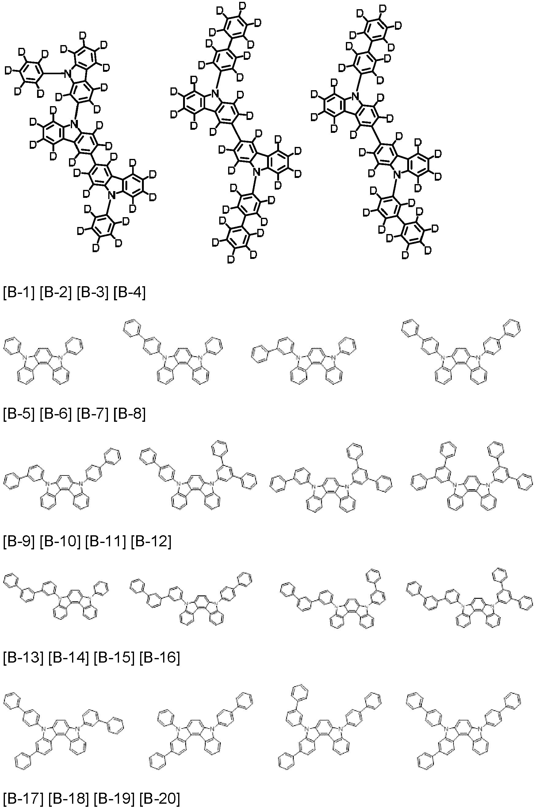
- the second compound may be one selected from compounds of Group 2, but is not limited thereto.
- the first compound and the second compound may be for example included in a weight ratio of 1:99 to 99:1.
- a desirable weight ratio may be adjusted using an electron transport capability of the first compound and a hole transport capability of the second compound to realize bipolar characteristics and thus to improve efficiency and life-span.
- they may be for example included in a weight ratio of about 10:90 to 90:10, about 20:80 to 80:20, for example about 20:80 to about 70: 30, about 20:80 to about 60:40, or about 30:70 to about 60:40.
- they may be included in a weight ratio of 40:60, 50:50, or 60:40.
- One or more compounds may be included in addition to the aforementioned first compound and second compound.
- the aforementioned compound for an organic optoelectronic device or composition for an organic optoelectronic device may further include a dopant.
- the dopant may be, for example, a phosphorescent dopant, for example, a red, green, or blue phosphorescent dopant, for example, a red or green phosphorescent dopant.
- the dopant is a material mixed with the compound or composition for an organic optoelectronic device in a small amount to cause light emission, and may be generally a material such as a metal complex that emits light by multiple excitation into a triplet or more.
- the dopant may be, for example, an inorganic, organic, or organic-inorganic compound, and one or more types thereof may be used.
- Examples of the dopant may be a phosphorescent dopant and examples of the phosphorescent dopant may be an organic metal compound including Ir, Pt, Os, Ti, Zr, Hf, Eu, Tb, Tm, Fe, Co, Ni, Ru, Rh, Pd, or a combination thereof.
- the phosphorescent dopant may be, for example, a compound represented by Chemical Formula Z, but is not limited thereto. [Chemical Formula Z] L 7 MX
- M is a metal
- L 7 and X are the same or different, and are a ligand to form a complex compound with M.
- the M may be for example Ir, Pt, Os, Ti, Zr, Hf, Eu, Tb, Tm, Fe, Co, Ni, Ru, Rh, Pd, or a combination thereof and L 1 and X 3 may be, for example a bidendate ligand.
- the aforementioned compound for an organic optoelectronic device or composition for an organic optoelectronic device may be formed into a film by a dry film formation method such as chemical vapor deposition (CVD).
- CVD chemical vapor deposition
- an organic optoelectronic device including the aforementioned compound for an organic optoelectronic device or composition for an organic optoelectronic device is described.
- the organic optoelectronic device may be any device to convert electrical energy into photoenergy and vice versa without particular limitation, and may be, for example an organic photoelectric device, an organic light emitting diode, an organic solar cell, and an organic photoconductor drum.
- FIGS. 1 to 4 are cross-sectional views showing organic light emitting diodes according to embodiments.
- an organic light emitting diode 100 includes an anode 120 and a cathode 110 facing each other and an organic layer 105 disposed between the anode 120 and cathode 110.
- the anode 120 may be made of a conductor having a large work function to help hole injection, and may be for example a metal, a metal oxide and/or a conductive polymer.
- the anode 120 may be, for example a metal such as nickel, platinum, vanadium, chromium, copper, zinc, gold, and the like or an alloy thereof; a metal oxide such as zinc oxide, indium oxide, indium tin oxide (ITO), indium zinc oxide (IZO), and the like; a combination of a metal and an oxide such as ZnO and Al or SnO 2 and Sb; a conductive polymer such as poly(3-methylthiophene), poly(3,4-(ethylene-1,2-dioxy)thiophene) (PEDOT), polypyrrole, and polyaniline, but is not limited thereto.
- the cathode 110 may be made of a conductor having a small work function to help electron injection, and may be for example a metal, a metal oxide, and/or a conductive polymer.
- the cathode 110 may be for example a metal such as magnesium, calcium, sodium, potassium, titanium, indium, yttrium, lithium, gadolinium, aluminum silver, tin, lead, cesium, barium, and the like, or an alloy thereof; a multi-layer structure material such as LiF/Al, LiO 2 /Al, LiF/Ca, LiF/Al, and BaF 2 /Ca, but is not limited thereto.
- the organic layer 105 may include the aforementioned compound for an organic optoelectronic device or composition for an organic optoelectronic device.
- the organic layer 105 may include the light emitting layer 130, and the light emitting layer 130 may include the aforementioned compound for an organic optoelectronic device or composition for an organic optoelectronic device.
- composition for an organic optoelectronic device further including a dopant may be, for example, a green light emitting composition.
- the light emitting layer 130 may include, for example, the aforementioned compound for an organic optoelectronic device or composition for an organic optoelectronic device, respectively, as a phosphorescent host.
- the organic layer may further include a charge transport region in addition to the light emitting layer.
- the charge transport region may be, for example, the hole transport region 140.
- the organic light emitting diode 200 further includes a hole transport region 140 in addition to the light emitting layer 130.
- the hole transport region 140 may further increase hole injection and/or hole mobility and block electrons between the anode 120 and the light emitting layer 130.
- the hole transport region 140 may include a hole transport layer between the anode 120 and the light emitting layer 130, and a hole transport auxiliary layer between the light emitting layer 130 and the hole transport layer, and at least one of the compounds of Group A may be included in at least one of the hole transport layer and the hole transport auxiliary layer.
- the charge transport region may be, for example, an electron transport region 150.
- the organic light emitting diode 300 further includes an electron transport region 150 in addition to the light emitting layer 130.
- the electron transport region 150 may further increase electron injection and/or electron mobility and block holes between the cathode 110 and the light emitting layer 130.
- the electron transport region 150 may include an electron transport layer between the cathode 110 and the light emitting layer 130, and an electron transport auxiliary layer between the light emitting layer 130 and the electron transport layer, and at least one of the compounds of Group B may be included in at least one of the electron transport layer and the electron transport auxiliary layer.
- An example embodiment of the present invention may be an organic light emitting diode including the light emitting layer 130 as the organic layer 105 as shown in FIG. 1 .
- Another embodiment of the present invention may be an organic light emitting diode including a hole transport region 140 in addition to the light emitting layer 130 as the organic layer 105 as shown in FIG. 2 .
- Another embodiment of the present invention may be an organic light emitting diode including an electron transport region 150 in addition to the light emitting layer130 as the organic layer 105 as shown in FIG. 3 .
- Another embodiment of the present invention may be an organic light emitting diode including a hole transport region 140 and an electron transport region 150 in addition to the light emitting layer130 as the organic layer 105 as shown in FIG. 4 .
- Another embodiment of the present invention may be an organic light emitting diode further including an electron injection layer (not shown), a hole injection layer (not shown), etc. in addition to the light emitting layer 130 as the organic layer 105 in each of FIGS. 1 to 4 .
- the organic light emitting diodes 100, 200, 300, and 400 may be produced by forming an anode or a cathode on a substrate, forming an organic layer using a dry film formation method such as a vacuum deposition method (evaporation), sputtering, plasma plating, and ion plating, and forming a cathode or an anode thereon.
- a dry film formation method such as a vacuum deposition method (evaporation), sputtering, plasma plating, and ion plating, and forming a cathode or an anode thereon.
- the organic light emitting diode may be applied to an organic light emitting display device.
- the glass substrate coated with ITO Indium tin oxide was washed with distilled water and ultrasonic waves. After washing with the distilled water, the glass substrate was washed with a solvent such as isopropyl alcohol, acetone, methanol, and the like ultrasonically and dried and then, moved to a plasma cleaner, cleaned by using oxygen plasma for 10 minutes, and moved to a vacuum depositor.
- a solvent such as isopropyl alcohol, acetone, methanol, and the like ultrasonically and dried and then, moved to a plasma cleaner, cleaned by using oxygen plasma for 10 minutes, and moved to a vacuum depositor.
- ITO transparent electrode was used as an anode, Compound A doped with 3% NDP-9 (available from Novaled) was vacuum-deposited on the ITO substrate to form a 50 ⁇ -thick hole injection layer, and Compound A was deposited on the hole injection layer to form a 1350 ⁇ -thick hole transport layer, and Compound B was deposited on the hole transport layer to form a 350 ⁇ -thick hole transport auxiliary layer.
- 400 ⁇ -thick light emitting layer was formed by using Compound 1-3 of Synthesis Example 1 as a host and doping 10 wt% of PhGD as a dopant.
- Compound C was deposited on the light emitting layer to form a 50 ⁇ -thick electron transport auxiliary layer, and Compound D and Liq were simultaneously vacuum-deposited at a weight ratio of 1:1 to form a 300 ⁇ -thick electron transport layer.
- LiQ (15 ⁇ ) and Al (1200 ⁇ ) were sequentially vacuum-deposited on the electron transport layer to form a cathode, thereby manufacturing an organic light emitting diode.
- An organic light emitting diode was manufactured in the same manner as in Example 1 except that Compound 1 and Compound A-136 of Synthesis Example 2 were mixed in a weight ratio of 3:7 instead of Compound 1.
- An organic light emitting diode was manufactured in the same manner as in Example 1 except that Host 1 was used instead of Compound 1.
- An organic light emitting diode was manufactured in the same manner as in Example 1 except that Host 2 was used instead of Compound 1.
- An organic light emitting diode was manufactured in the same manner as in Example 1 except that Host 3 was used instead of Compound 1.
- An organic light emitting diode was manufactured in the same manner as in Example 1 except that Host 1 of Comparative Synthesis Example 1 and Compound A-136 were mixed in a weight ratio of 3:7 instead of Compound 1.
- An organic light emitting diode was manufactured in the same manner as in Example 1 except that Host 2 of Comparative Synthesis Example 2 and Compound A-136 were mixed in a weight ratio of 3:7 instead of Compound 1.
- An organic light emitting diode was manufactured in the same manner as in Example 1 except that Host 3 of Comparative Synthesis Example 3 and Compound A-141 were mixed in a weight ratio of 35:65 instead of Compound 1.
- the obtained organic light emitting diodes were measured regarding a current value flowing in the unit device, while increasing the voltage from 0 V to 10 V using a current-voltage meter (Keithley 2400), and the measured current value was divided by area to provide the results.
- Luminance was measured by using a luminance meter (Minolta Cs-1000A), while the voltage of the organic light emitting diodes was increased from 0 V to 10 V.
- the driving voltage of each diode was measured at 15mA/cm 2 using a current-voltmeter (Keithley 2400) to obtain the results.
- Table 1 The values shown in Table 1 are relative values based on the values of Example 1, respectively.
- Table 2 The values shown in Table 2 are relative values based on the values of Example 2, respectively.
- Table 1 Nos. Compound Driving voltage (V)% Color (EL color) Luminous efficiency (%) Life-span (T97@18K) (%)
- Example 1 1-3 100% Green 100% 100% Compar ative Example 1 Host1 101.0% Green 96.4% 88.2% Compar ative Example 2 Host2 107.6% Green 99.2% 94.1% Compar ative Example 3 Host3 100.8% Green 82.7% 88.2%
- Example 2 the driving voltage, luminous efficiency, and life-span characteristic of the organic light emitting diode according to Example 1 was significantly improved, compared with the organic light emitting diodes according to Comparative Examples 1 to 3.
- Table 2 No. Compound (first host) Compound (second host) Color (EL color) Luminous efficiency (cd/A) Life-span (T97@18K) (h)
- Example 2 1-3 A-136 Green 100% 100% Compar ative Example 4
- Comparative Example 5 Host2 A-136 Green 95.7% 93.0% Compar ative Example 6
- the organic light emitting diode according to Example 2 exhibited significantly improved luminous efficiency and life-span characteristics compared with the organic light emitting diodes according to Comparative Examples 4 to 6.
Landscapes
- Chemical & Material Sciences (AREA)
- Physics & Mathematics (AREA)
- Organic Chemistry (AREA)
- Spectroscopy & Molecular Physics (AREA)
- Engineering & Computer Science (AREA)
- Materials Engineering (AREA)
- Optics & Photonics (AREA)
- Electroluminescent Light Sources (AREA)
- Light Receiving Elements (AREA)
- Nitrogen Condensed Heterocyclic Rings (AREA)
- Organic Low-Molecular-Weight Compounds And Preparation Thereof (AREA)
- Indole Compounds (AREA)
Abstract
Description
- A compound for an organic optoelectronic device, a composition for an organic optoelectronic device, an organic optoelectronic device, and a display device are disclosed.
- An organic optoelectronic device (organic optoelectronic diode) is a device capable of converting electrical energy and optical energy to each other.
- Organic optoelectronic devices may be largely divided into two types according to a principle of operation. One is a photoelectric device that generates electrical energy by separating excitons formed by light energy into electrons and holes, and transferring the electrons and holes to different electrodes, respectively and the other is light emitting device that generates light energy from electrical energy by supplying voltage or current to the electrodes.
- Examples of the organic optoelectronic device include an organic photoelectric device, an organic light emitting diode, an organic solar cell, and an organic photoconductor drum.
- Among them, organic light emitting diodes (OLEDs) are attracting much attention in recent years due to increasing demands for flat panel display devices. The organic light emitting diode is a device that converts electrical energy into light, and the performance of the organic light emitting diode is greatly influenced by an organic material between electrodes.
- An example embodiment provides a compound for an organic optoelectronic device having high efficiency and a long life-span.
- Another example embodiment provides a composition for an organic optoelectronic device including the compound for an organic optoelectronic device.
- Another example embodiment provides an organic optoelectronic device including the compound for an organic optoelectronic device or the composition for an organic optoelectronic device.
- Another example embodiment provides a display device including the organic optoelectronic device.
- According to an example embodiment, a compound for an organic optoelectronic device represented by a combination of Chemical Formula 1 and Chemical Formula 2 is provided.


- In Chemical Formula 1 and Chemical Formula 2,
- adjacent two of a1* to a4* of Chemical Formula 1 are each independently linking carbon linked to * in Chemical Formula 2,
- the rest two of a1* to a4* of Chemical Formula 1 not linked to * in Chemical Formula 2 are each independently C-La-Ra,
- Ar1 and Ar2 are each independently a substituted or unsubstituted C6 to C30 aryl group or a substituted or unsubstituted C2 to C30 heterocyclic group,
- Ar3 is a substituted or unsubstituted C6 to C20 aryl group,
- La, L1, and L2 are each independently a single bond, a substituted or unsubstituted C6 to C30 arylene group or a substituted or unsubstituted C2 to C30 heterocyclic group, and
- Ra, and R1 to R8 are each independently hydrogen, deuterium, a halogen, a substituted or unsubstituted C1 to C30 alkyl group, or a substituted or unsubstituted C6 to C30 aryl group.
- According to another embodiment, a composition for an organic optoelectronic device includes a first compound, and a second compound.
- The first compound is the same as described above, and the second compound may be a compound for an organic optoelectronic device represented by Chemical Formula 3; or a compound for an organic optoelectronic device represented by a combination of Chemical Formula 4 and Chemical Formula 5.
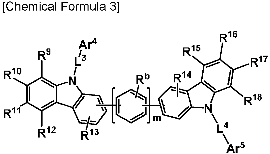
- Ar4 and Ar5 are each independently a substituted or unsubstituted C6 to C20 aryl group or a substituted or unsubstituted C2 to C30 heterocyclic group,
- L3 and L4 are each independently a single bond or a substituted or unsubstituted C6 to C20 arylene group,
- Rb and R9 to R18 are each independently hydrogen, deuterium, a cyano group, a halogen, a substituted or unsubstituted amino group, a substituted or unsubstituted C1 to C30 alkyl group, a substituted or unsubstituted C6 to C30 aryl group, or a substituted or unsubstituted C2 to C30 heterocyclic group, and
- m is an integer of 0 to 2;


- In Chemical Formulas 4 and 5,
- Ar6 and Ar7 are each independently a substituted or unsubstituted C6 to C20 aryl group or a substituted or unsubstituted C2 to C30 heterocyclic group,
- adjacent two of b1* to b4* of Chemical Formula 4 are each independently linking carbon linked to * in Chemical Formula 5,
- the rest two of b1* to b4* of Chemical Formula 4 not linked to * in Chemical Formula 5 are each independently C-Lb-Rc,
- Lb, L5, and L6 are each independently a single bond or a substituted or unsubstituted C6 to C20 arylene group,
- Rc and R19 to R26 are each independently hydrogen, deuterium, a cyano group, a halogen, a substituted or unsubstituted amino group, a substituted or unsubstituted C1 to C30 alkyl group, a substituted or unsubstituted C6 to C30 aryl group, or a substituted or unsubstituted C2 to C30 heterocyclic group.
- According to another embodiment, an organic optoelectronic device includes an anode and a cathode facing each other, and at least one organic layer between the anode and the cathode, wherein the organic layer includes the compound for an organic optoelectronic device or a composition for an organic optoelectronic device.
- According to another embodiment, a display device including the organic optoelectronic device is provided.
- An organic optoelectronic device having high efficiency and a long life-span may be realized.
-
FIGS. 1 to 4 are cross-sectional views each illustrating an organic light emitting diode according to embodiments. -
- 100, 200, 300, 400:
- organic light emitting diode
- 105:
- organic layer
- 110:
- cathode
- 120:
- anode
- 130:
- light emitting layer
- 140:
- hole transport region
- 150:
- electron transport region
- Hereinafter, embodiments of the present invention are described in detail. However, these embodiments are exemplary, the present invention is not limited thereto and the present invention is defined by the scope of claims.
- In the present specification, when a definition is not otherwise provided, "substituted" refers to replacement of at least one hydrogen of a substituent or a compound by deuterium, a halogen, a hydroxyl group, an amino group, a substituted or unsubstituted C1 to C30 amine group, a nitro group, a substituted or unsubstituted C1 to C40 silyl group, a C1 to C30 alkyl group, a C1 to C10 alkylsilyl group, a C6 to C30 arylsilyl group, a C3 to C30 cycloalkyl group, a C3 to C30 heterocycloalkyl group, a C6 to C30 aryl group, a C2 to C30 heteroaryl group, a C1 to C20 alkoxy group, a C1 to C10 trifluoroalkyl group, a cyano group, or a combination thereof.
- In one example of the present invention, the "substituted" refers to replacement of at least one hydrogen of a substituent or a compound by deuterium, a C1 to C30 alkyl group, a C1 to C10 alkylsilyl group, a C6 to C30 arylsilyl group, a C3 to C30 cycloalkyl group, a C3 to C30 heterocycloalkyl group, a C6 to C30 aryl group, a C2 to C30 heteroaryl group, or a cyano group. In specific example of the present invention, the "substituted" refers to replacement of at least one hydrogen of a substituent or a compound by deuterium, a C1 to C20 alkyl group, a C6 to C30 aryl group, or a cyano group. In specific example of the present invention, the "substituted" refers to replacement of at least one hydrogen of a substituent or a compound by deuterium, a C1 to C5 alkyl group, a C6 to C18 aryl group, or a cyano group. In specific example of the present invention, the "substituted" refers to replacement of at least one hydrogen of a substituent or a compound by deuterium, a cyano group, a methyl group, an ethyl group, a propyl group, a butyl group, a phenyl group, a biphenyl group, a terphenyl group, or a naphthyl group.
- In the present specification, when a definition is not otherwise provided, "hetero" refers to one including one to three heteroatoms selected from N, O, S, P, and Si, and remaining carbons in one functional group.
- In the present specification, "an aryl group" refers to a group including at least one hydrocarbon aromatic moiety, and all elements of the hydrocarbon aromatic moiety have p-orbitals which form conjugation, for example a phenyl group, a naphthyl group, and the like, two or more hydrocarbon aromatic moieties may be linked by a sigma bond and may be, for example a biphenyl group, a terphenyl group, a quarterphenyl group, and the like, and two or more hydrocarbon aromatic moieties are fused directly or indirectly to provide a nonaromatic fused ring, for example a fluorenyl group.
- The aryl group may include a monocyclic, polycyclic, or fused ring polycyclic (i.e., rings sharing adjacent pairs of carbon atoms) functional group.
- In the present specification, "a heterocyclic group" is a generic concept of a heteroaryl group, and may include at least one heteroatom selected from N, O, S, P, and Si instead of carbon (C) in a cyclic compound such as an aryl group, a cycloalkyl group, a fused ring thereof, or a combination thereof. When the heterocyclic group is a fused ring, the entire ring or each ring of the heterocyclic group may include one or more heteroatoms.
- For example, "a heteroaryl group" may refer to an aryl group including at least one heteroatom selected from N, O, S, P, and Si. Two or more heteroaryl groups are linked by a sigma bond directly, or when the heteroaryl group includes two or more rings, the two or more rings may be fused. When the heteroaryl group is a fused ring, each ring may include one to three heteroatoms.
- More specifically, the substituted or unsubstituted C6 to C30 aryl group may be a substituted or unsubstituted phenyl group, a substituted or unsubstituted naphthyl group, a substituted or unsubstituted anthracenyl group, a substituted or unsubstituted phenanthrenyl group, a substituted or unsubstituted naphthacenyl group, a substituted or unsubstituted pyrenyl group, a substituted or unsubstituted biphenyl group, a substituted or unsubstituted p-terphenyl group, a substituted or unsubstituted m-terphenyl group, a substituted or unsubstituted o-terphenyl group, a substituted or unsubstituted chrysenyl group, a substituted or unsubstituted triphenylene group, a substituted or unsubstituted perylenyl group, a substituted or unsubstituted fluorenyl group, a substituted or unsubstituted indenyl group, a substituted or unsubstituted furanyl group, or a combination thereof, but is not limited thereto.
- More specifically, the substituted or unsubstituted C2 to C30 heterocyclic group may be a substituted or unsubstituted thiophenyl group, a substituted or unsubstituted pyrrolyl group, a substituted or unsubstituted pyrazolyl group, a substituted or unsubstituted imidazolyl group, a substituted or unsubstituted triazolyl group, a substituted or unsubstituted oxazolyl group, a substituted or unsubstituted thiazolyl group, a substituted or unsubstituted oxadiazolyl group, a substituted or unsubstituted thiadiazolyl group, a substituted or unsubstituted pyridyl group, a substituted or unsubstituted pyrimidinyl group, a substituted or unsubstituted pyrazinyl group, a substituted or unsubstituted triazinyl group, a substituted or unsubstituted benzofuranyl group, a substituted or unsubstituted benzothiophenyl group, a substituted or unsubstituted benzimidazolyl group, a substituted or unsubstituted indolyl group, a substituted or unsubstituted quinolinyl group, a substituted or unsubstituted isoquinolinyl group, a substituted or unsubstituted quinazolinyl group, a substituted or unsubstituted quinoxalinyl group, a substituted or unsubstituted naphthyridinyl group, a substituted or unsubstituted benzoxazinyl group, a substituted or unsubstituted benzthiazinyl group, a substituted or unsubstituted arcridinyl group, a substituted or unsubstituted phenazinyl group, a substituted or unsubstituted phenothiazinyl group, a substituted or unsubstituted phenoxazinyl group, a substituted or unsubstituted carbazolyl group, a substituted or unsubstituted dibenzofuranyl group, or a substituted or unsubstituted dibenzothiophenyl group, or a combination thereof, but is not limited thereto.
- In the present specification, hole characteristics refer to an ability to donate an electron to form a hole when an electric field is applied and that a hole formed in the anode may be easily injected into the light emitting layer and transported in the light emitting layer due to conductive characteristics according to a highest occupied molecular orbital (HOMO) level.
- In addition, electron characteristics refer to an ability to accept an electron when an electric field is applied and that electron formed in the cathode may be easily injected into the light emitting layer and transported in the light emitting layer due to conductive characteristics according to a lowest unoccupied molecular orbital (LUMO) level.
- Hereinafter, a compound for an organic optoelectronic device according to an example embodiment is described.
- A compound for an organic optoelectronic device according to an example embodiment is represented by a combination of Chemical Formula 1 and Chemical Formula 2.

- In Chemical Formula 1 and Chemical Formula 2,
- adjacent two of a1* to a4* of Chemical Formula 1 are each independently linking carbon linked to * in Chemical Formula 2,
- the rest two of a1* to a4* of Chemical Formula 1 not linked to * in Chemical Formula 2 are each independently C-La-Ra,
- Ar1 and Ar2 are each independently a substituted or unsubstituted C6 to C30 aryl group or a substituted or unsubstituted C2 to C30 heterocyclic group,
- Ar3 is a substituted or unsubstituted C6 to C20 aryl group,
- La, L1, and L2 are each independently a single bond, a substituted or unsubstituted C6 to C30 arylene group or a substituted or unsubstituted C2 to C30 heterocyclic group, and
- Ra, and R1 to R8 are each independently hydrogen, deuterium, a halogen, a substituted or unsubstituted C1 to C30 alkyl group, or a substituted or unsubstituted C6 to C30 aryl group.
- In the compound represented by the combination of Chemical Formula 1 and Chemical Formula 2, one of the substituents in the N direction of the indolocarbazole core is a substituted or unsubstituted triazine group, and the other is a phenylene moiety having a phenyl group in the ortho direction and an additional substituent in the other direction.
- In this structure, the triazine and the ortho-phenylene moiety including the additional substituent in the indolocarbazole skeleton in which the N-direction substituents are positioned in parallel have a steric structural hindrance to each other, thereby reducing a degree of freedom of the molecule and arranging the molecules in a certain direction. This increases intermolecular orientation to increase intermolecular electron and hole mobility, and relatively high efficiency and life-span may be exhibited.
- The combination of Chemical Formula 1 and Chemical Formula 2 may be represented by one of Chemical Formula 1A to Chemical Formula 1F.


- In Chemical Formula 1A to Chemical Formula 1F,
- Ar1 to Ar3, L1, L2, and R1 to R8 are the same as described above,
- La1 to La4 are the same as the definition of La described above, and
- Ra1 to Ra4 are the same as the definition of Ra described above.
- For example, the combination of Chemical Formula 1 and Chemical Formula 2 may be represented by Chemical Formula 1B.
- As a specific example, Chemical Formula 1B may be represented by, for example, one of Chemical Formula 1B-1 to Chemical Formula 1B-4, depending on a substitution direction of the additional substituent included in the ortho-phenylene moiety in the indolocarbazole skeleton.


- In Chemical Formula 1B-1 to Chemical Formula 1B-4,
Ar1 to Ar3, L1, L2, La3, La4, and R1 to R8 are the same as described above. - In an example embodiment, Ar3 may be a substituted or unsubstituted phenyl group, a substituted or unsubstituted biphenyl group, a substituted or unsubstituted terphenyl group, a substituted or unsubstituted naphthyl group, a substituted or unsubstituted anthracenyl group, a substituted or unsubstituted phenanthrenyl group, or a substituted or unsubstituted triphenylene group.
- In an example embodiment, Ar1 and Ar2 may each independently be a substituted or unsubstituted phenyl group, a substituted or unsubstituted biphenyl group, a substituted or unsubstituted terphenyl group, a substituted or unsubstituted naphthyl group, a substituted or unsubstituted anthracenyl group, a substituted or unsubstituted phenanthrenyl group, a substituted or unsubstituted triphenylene group, a substituted or unsubstituted fluorenyl group, a substituted or unsubstituted dibenzofuranyl group, a substituted or unsubstituted dibenzothiophenyl group, or a substituted or unsubstituted dibenzosilolyl group.
- In a specific example embodiment, Ar1 and Ar2 may each independently be a substituted or unsubstituted phenyl group, a substituted or unsubstituted biphenyl group, a substituted or unsubstituted terphenyl group, a substituted or unsubstituted quaterphenyl group, or a substituted or unsubstituted naphthyl group.
- In an example embodiment, L1 and L2 may each independently be a single bond, a substituted or unsubstituted phenylene group, a substituted or unsubstituted biphenylene group, a substituted or unsubstituted dibenzofuranylene group, or a substituted or unsubstituted dibenzothiophenylene group.
- In a specific embodiment, L1 to L3 may each independently be a single bond, or a substituted or unsubstituted phenylene group.
- For example, *-L1-Ar1 and *-L2-Ar2 may be each independently selected from substituents of Group I .

- In Group I , * is a linking point.
- When Ar1 and Ar2 are substituted, the substituent may be a C6 to C12 aryl group. More specifically, the substituent may be a phenyl group.
- For example, at least one of Ar1 and Ar2 may be a substituted or unsubstituted C10 to C30 aryl group.
- In a specific example, at least one of Ar1 and Ar2 may be a substituted or unsubstituted biphenyl group, a substituted or unsubstituted terphenyl group, a substituted or unsubstituted naphthyl group, a substituted or unsubstituted anthracenyl group, a substituted or unsubstituted phenanthrenyl group, a substituted or unsubstituted triphenylene group, or a substituted or unsubstituted fluorenyl group.
- In an example embodiment, R1 to R8 may each independently be hydrogen or a substituted or unsubstituted phenyl group.
- In a specific embodiment, each of R1 to R8 may be hydrogen.
- The more specific example of the compound for an organic optoelectronic device represented by the combination of Chemical Formula 1 and Chemical Formula 2 may include the compounds of Group 1, but is not limited thereto.


- A composition for an organic optoelectronic device according to another embodiment includes a first compound, and a second compound, wherein the first compound may be the aforementioned compound for an organic optoelectronic device and the second compound may be a compound for an organic optoelectronic device represented by Chemical Formula 3; or a compound for an organic optoelectronic device represented by the combination of Chemical Formula 4 and Chemical Formula 5.

- In Chemical Formula 3,
- Ar4 and Ar5 are each independently a substituted or unsubstituted C6 to C20 aryl group or a substituted or unsubstituted C2 to C30 heterocyclic group,
- L3 and L4 are each independently a single bond or a substituted or unsubstituted C6 to C20 arylene group,
- Rb and R9 to R18 are each independently hydrogen, deuterium, a cyano group, a halogen, a substituted or unsubstituted amino group, a substituted or unsubstituted C1 to C30 alkyl group, a substituted or unsubstituted C6 to C30 aryl group, or a substituted or unsubstituted C2 to C30 heterocyclic group, and
- m is an integer of 0 to 2;
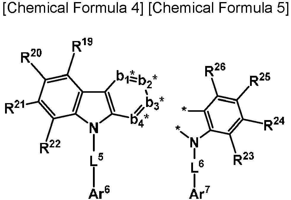
- In Chemical Formulas 4 and 5,
- Ar6 and Ar7 are each independently a substituted or unsubstituted C6 to C20 aryl group or a substituted or unsubstituted C2 to C30 heterocyclic group,
- adjacent two of b1* to b4* of Chemical Formula 4 are each independently linking carbon linked to * in Chemical Formula 5,
- the rest two of b1* to b4* of Chemical Formula 4 not linked to * in Chemical Formula 5 are each independently C-Lb-Rc,
- Lb, L5, and L6 are each independently a single bond or a substituted or unsubstituted C6 to C20 arylene group, and
- Rc and R19 to R26 are each independently hydrogen, deuterium, a cyano group, a halogen, a substituted or unsubstituted amino group, a substituted or unsubstituted C1 to C30 alkyl group, a substituted or unsubstituted C6 to C30 aryl group, or a substituted or unsubstituted C2 to C30 heterocyclic group.
- The second compound may be used in the light emitting layer together with the first compound to increase mobility of charges and improve stability, thereby improving luminous efficiency and life-span characteristics.
- For example, Ar4 and Ar5 of Chemical Formula 3 may each independently be a substituted or unsubstituted phenyl group, a substituted or unsubstituted biphenyl group, a substituted or unsubstituted terphenyl group, a substituted or unsubstituted naphthyl group, a substituted or unsubstituted anthracenyl group, a substituted or unsubstituted triphenylenyl group, a substituted or unsubstituted carbazolyl group, a substituted or unsubstituted dibenzothiophenyl group, a substituted or unsubstituted dibenzofuranyl group, or a substituted or unsubstituted fluorenyl group,
- L3 and L4 of Chemical Formula 3 may each independently be a single bond, a substituted or unsubstituted phenylene group, or a substituted or unsubstituted biphenylene group,
- Rb and R9 to R18 of Chemical Formula 3 may each independently be hydrogen, deuterium, or a substituted or unsubstituted C6 to C12 aryl group,
- m may be 0 or 1.
- "Substituted" of Chemical Formula 3 refers to replacement of at least one hydrogen by deuterium, a C1 to C4 alkyl group, a C6 to C18 aryl group, or a C2 to C30 heteroaryl group.
- In a specific embodiment of the present invention, Chemical Formula 3 may be represented by one of Chemical Formula 3-1 to Chemical Formula 3-15.


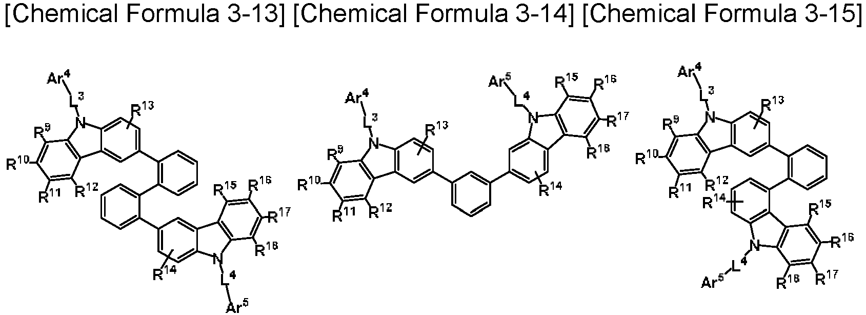
- In Chemical Formula 3-1 to Chemical Formula 3-15, R9 to R18 may each independently be hydrogen or a substituted or unsubstituted C6 to C12 aryl group, and *-L3-Ar4 and *-L4-Ar5 may each independently be one of substituents of Group II.

- In Group II, * is a linking point.
- In an example embodiment, Chemical Formula 3 may be represented by Chemical Formula 3-8.
- In addition, *-L3-Ar4 and *-L4-Ar5 of Chemical Formula 3-8 may each independently be selected from Group II, and may be, for example, one of C-1, C-2, C-3, C-4, C -7, C-8, and C-9.
- For example, the second compound represented by the combination of Chemical Formula 4 and Chemical Formula 5 may be represented by one of Chemical Formula Chemical Formula 4A, Chemical Formula 4B, Chemical Formula 4C, Chemical Formula 4D and Chemical Formula 4E.


- In Chemical Formula 4A to Chemical Formula 4E, Ar6, Ar7, L5, L6, and R19 to R26 are the same as described above,
- Lb1 to Lb4 are the same as the definitions of L5 and L6 described above, and
- Rc1 to Rc4 have the same definitions as R19 to R26 described above.
- For example, Ar6 and Ar7 of Chemical Formulas 4 and 5 may each independently be a substituted or unsubstituted phenyl group, a substituted or unsubstituted biphenyl group, a substituted or unsubstituted pyridinyl group, a substituted or unsubstituted carbazolyl group, a substituted or unsubstituted dibenzofuranyl group, or a substituted or unsubstituted dibenzothiophenyl group, and
- Rc1 to Rc4 and R19 to R26 may each independently be hydrogen, deuterium, a cyano group, a substituted or unsubstituted phenyl group, a substituted or unsubstituted biphenyl group, a substituted or unsubstituted pyridinyl group, a substituted or unsubstituted carbazolyl group, a substituted or unsubstituted dibenzofuranyl group, or a substituted or unsubstituted dibenzothiophenyl group.
- In a specific embodiment of the present invention, Ar6 and Ar7 in Chemical Formulas 4 and 5 may be each independently selected from the substituents of Group II.
- In an example embodiment, Rc1 to Rc4 and R19 to R26 may each independently be hydrogen, deuterium, a cyano group, a substituted or unsubstituted phenyl group, a substituted or unsubstituted biphenyl group, a substituted or unsubstituted pyridinyl group, a substituted or unsubstituted carbazolyl group, a substituted or unsubstituted dibenzofuranyl group, or a substituted or unsubstituted dibenzothiophenyl group.
- For example, Rc1 to Rc4 and R19 to R26 may each independently be hydrogen, deuterium, a cyano group, or a substituted or unsubstituted phenyl group, and
in a specific example embodiment, Rc1 to Rc4, and R19 to R26 may each independently be hydrogen, or a phenyl group. - In a specific example embodiment, the second compound may be represented by Chemical Formula 3-8, wherein Ar4 and Ar6 of Chemical Formula 3-8 may each independently be a substituted or unsubstituted phenyl group, a substituted or unsubstituted biphenyl group, a substituted or unsubstituted pyridinyl group, a substituted or unsubstituted carbazolyl group, a substituted or unsubstituted dibenzofuranyl group, or a substituted or unsubstituted dibenzothiophenyl group, L3 and L4 may each independently be a single bond, or a substituted or unsubstituted C6 to C20 arylene group, R9 to R18 may each independently be hydrogen, deuterium, a cyano group, a substituted or unsubstituted phenyl group, a substituted or unsubstituted biphenyl group, a substituted or unsubstituted pyridinyl group, a substituted or unsubstituted carbazolyl group, a substituted or unsubstituted dibenzofuranyl group, or a substituted or unsubstituted dibenzothiophenyl group.
- In another specific example embodiment, the second compound may be represented by Chemical Formula 4C, wherein Lb1 to Lb4 of Chemical Formula 4C may be a single bond, L5 and L6 may each independently be a single bond or a substituted or unsubstituted C6 to C12 arylene group, R19 to R26, Rc1 to Rc4 may each independently be hydrogen or a phenyl group, and Ar6 and Ar7 may each independently be a substituted or unsubstituted phenyl group, a substituted or unsubstituted biphenyl group, or a substituted or unsubstituted terphenyl group.
- For example, the second compound may be one selected from compounds of Group 2, but is not limited thereto.




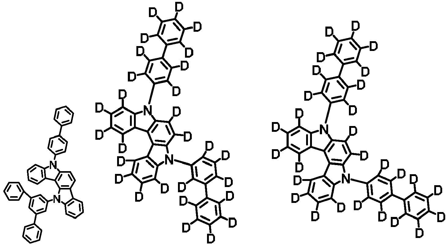
- The first compound and the second compound may be for example included in a weight ratio of 1:99 to 99:1. Within the range, a desirable weight ratio may be adjusted using an electron transport capability of the first compound and a hole transport capability of the second compound to realize bipolar characteristics and thus to improve efficiency and life-span. Within the range, they may be for example included in a weight ratio of about 10:90 to 90:10, about 20:80 to 80:20, for example about 20:80 to about 70: 30, about 20:80 to about 60:40, or about 30:70 to about 60:40. As a specific example, they may be included in a weight ratio of 40:60, 50:50, or 60:40.
- One or more compounds may be included in addition to the aforementioned first compound and second compound.
- The aforementioned compound for an organic optoelectronic device or composition for an organic optoelectronic device may further include a dopant.
- The dopant may be, for example, a phosphorescent dopant, for example, a red, green, or blue phosphorescent dopant, for example, a red or green phosphorescent dopant.
- The dopant is a material mixed with the compound or composition for an organic optoelectronic device in a small amount to cause light emission, and may be generally a material such as a metal complex that emits light by multiple excitation into a triplet or more. The dopant may be, for example, an inorganic, organic, or organic-inorganic compound, and one or more types thereof may be used.
- Examples of the dopant may be a phosphorescent dopant and examples of the phosphorescent dopant may be an organic metal compound including Ir, Pt, Os, Ti, Zr, Hf, Eu, Tb, Tm, Fe, Co, Ni, Ru, Rh, Pd, or a combination thereof. The phosphorescent dopant may be, for example, a compound represented by Chemical Formula Z, but is not limited thereto.
[Chemical Formula Z] L7MX
- In Chemical Formula Z, M is a metal, and L7 and X are the same or different, and are a ligand to form a complex compound with M.
- The M may be for example Ir, Pt, Os, Ti, Zr, Hf, Eu, Tb, Tm, Fe, Co, Ni, Ru, Rh, Pd, or a combination thereof and L1 and X3 may be, for example a bidendate ligand.
- The aforementioned compound for an organic optoelectronic device or composition for an organic optoelectronic device may be formed into a film by a dry film formation method such as chemical vapor deposition (CVD).
- Hereinafter, an organic optoelectronic device including the aforementioned compound for an organic optoelectronic device or composition for an organic optoelectronic device is described.
- The organic optoelectronic device may be any device to convert electrical energy into photoenergy and vice versa without particular limitation, and may be, for example an organic photoelectric device, an organic light emitting diode, an organic solar cell, and an organic photoconductor drum.
- Herein, an organic light emitting diode as one example of an organic optoelectronic device is described referring to drawings.
-
FIGS. 1 to 4 are cross-sectional views showing organic light emitting diodes according to embodiments. - Referring to
FIG. 1 , an organiclight emitting diode 100 according to an embodiment includes ananode 120 and acathode 110 facing each other and anorganic layer 105 disposed between theanode 120 andcathode 110. - The
anode 120 may be made of a conductor having a large work function to help hole injection, and may be for example a metal, a metal oxide and/or a conductive polymer. Theanode 120 may be, for example a metal such as nickel, platinum, vanadium, chromium, copper, zinc, gold, and the like or an alloy thereof; a metal oxide such as zinc oxide, indium oxide, indium tin oxide (ITO), indium zinc oxide (IZO), and the like; a combination of a metal and an oxide such as ZnO and Al or SnO2 and Sb; a conductive polymer such as poly(3-methylthiophene), poly(3,4-(ethylene-1,2-dioxy)thiophene) (PEDOT), polypyrrole, and polyaniline, but is not limited thereto. - The
cathode 110 may be made of a conductor having a small work function to help electron injection, and may be for example a metal, a metal oxide, and/or a conductive polymer. Thecathode 110 may be for example a metal such as magnesium, calcium, sodium, potassium, titanium, indium, yttrium, lithium, gadolinium, aluminum silver, tin, lead, cesium, barium, and the like, or an alloy thereof; a multi-layer structure material such as LiF/Al, LiO2/Al, LiF/Ca, LiF/Al, and BaF2/Ca, but is not limited thereto. - The
organic layer 105 may include the aforementioned compound for an organic optoelectronic device or composition for an organic optoelectronic device. - The
organic layer 105 may include thelight emitting layer 130, and thelight emitting layer 130 may include the aforementioned compound for an organic optoelectronic device or composition for an organic optoelectronic device. - The composition for an organic optoelectronic device further including a dopant may be, for example, a green light emitting composition.
- The
light emitting layer 130 may include, for example, the aforementioned compound for an organic optoelectronic device or composition for an organic optoelectronic device, respectively, as a phosphorescent host. - The organic layer may further include a charge transport region in addition to the light emitting layer.
- The charge transport region may be, for example, the
hole transport region 140. - Referring to
FIG. 2 , the organiclight emitting diode 200 further includes ahole transport region 140 in addition to thelight emitting layer 130. Thehole transport region 140 may further increase hole injection and/or hole mobility and block electrons between theanode 120 and thelight emitting layer 130. Specifically, thehole transport region 140 may include a hole transport layer between theanode 120 and thelight emitting layer 130, and a hole transport auxiliary layer between the light emittinglayer 130 and the hole transport layer, and at least one of the compounds of Group A may be included in at least one of the hole transport layer and the hole transport auxiliary layer.


- In the hole transport region, known compounds disclosed in
US5061569A ,JP1993-009471A WO1995-009147A1 ,JP1995-126615A JP1998-095973A - Also, the charge transport region may be, for example, an
electron transport region 150. - Referring to
FIG. 3 , the organiclight emitting diode 300 further includes anelectron transport region 150 in addition to thelight emitting layer 130. Theelectron transport region 150 may further increase electron injection and/or electron mobility and block holes between thecathode 110 and thelight emitting layer 130. - Specifically, the
electron transport region 150 may include an electron transport layer between thecathode 110 and thelight emitting layer 130, and an electron transport auxiliary layer between the light emittinglayer 130 and the electron transport layer, and at least one of the compounds of Group B may be included in at least one of the electron transport layer and the electron transport auxiliary layer.


- An example embodiment of the present invention may be an organic light emitting diode including the
light emitting layer 130 as theorganic layer 105 as shown inFIG. 1 . - Another embodiment of the present invention may be an organic light emitting diode including a
hole transport region 140 in addition to thelight emitting layer 130 as theorganic layer 105 as shown inFIG. 2 . - Another embodiment of the present invention may be an organic light emitting diode including an
electron transport region 150 in addition to the light emitting layer130 as theorganic layer 105 as shown inFIG. 3 . - Another embodiment of the present invention may be an organic light emitting diode including a
hole transport region 140 and anelectron transport region 150 in addition to the light emitting layer130 as theorganic layer 105 as shown inFIG. 4 . - Another embodiment of the present invention may be an organic light emitting diode further including an electron injection layer (not shown), a hole injection layer (not shown), etc. in addition to the
light emitting layer 130 as theorganic layer 105 in each ofFIGS. 1 to 4 . - The organic
light emitting diodes - The organic light emitting diode may be applied to an organic light emitting display device.
- Hereinafter, the embodiments are illustrated in more detail with reference to examples. However, these examples are exemplary, and the present scope is not limited thereto.
- Hereinafter, starting materials and reactants used in Examples and Synthesis Examples were purchased from Sigma-Aldrich Co. Ltd., TCI Inc., or Tokyo chemical industry as far as there is no particular comment or were synthesized by known methods.
-

-

- 50 g (166 mmol) of 4-bromo-2-fluoro-1-iodobenzene, 43 g (349 mmol) of phenylboronic acid, 13.4 g (11.6 mmol) of Pd(PPh3)4, 57 g (415 mmol) of K2CO3, 600 ml of toluene, 200 ml of ethanol, and 200 ml of purified water were put in a reactor and then, stirred under reflux, completing a reaction. The reactant was extracted with toluene and purified water and then, crystallized with methanol, obtaining 36 g of Int-1 (2'-fluoro-1,1'-4',1"-terphenyl, a white solid).
-

- 36 g (141 mmol) of 11,12-dihydroindolo[2,3-a]carbazole, 35 g (141 mmol) of Int-1, and 350 ml of N-Methyl-2-pyrrolidone were put in a reactor, and 6.8 g (170 mmol) of sodium hydride was added thereto and then, stirred under a nitrogen atmosphere. The reactant was stirred under reflux, completing a reaction. The reactant was cooled down, and purified water was added thereto to produce a solid and then, filtered and dried. The dried product was column-purified, obtaining 40 g of Intermediate Int-2 (light brown solid).
-

- 40 g (82.5 mmol) of Int-2, 34 g (100 mmol) of 2-([1,1'-biphenyl]-4-yl)-4-chloro-6-phenyl-1,3,5-triazine, 3.8 g (4.1 mmol) of Pd2(dba)3, 6 ml (12.3 mmol) of P(t-Bu)3, 16 g (165 mmol) of NaOt-Bu, and 400 ml of xylene were put in a reactor and stirred under reflux, completing a reaction. The reactant was cooled down and extracted with toluene and purified water, and an organic layer therefrom was concentrated. The concentrated product was column-purified, obtaining 34 g of Compound 1-3 (light yellow solid). (LC/MS: theoretical value 791.94 g/mol, measured value: 792.49 g/mol)
-


- 13.0 g (45.3 mmol) of 9-phenyl-9H-carbazole-3-boronic acid, 11.1 g (45.3 mmol) of 3-bromo-9H-carbazole, and 12.5 g (90.6 mmol) of K2CO3, and 2.62 g (2.2 mmol) of Pd(PPh3)4 were suspended in 3000 ml of THF and 110 ml of distilled water and then, stirred under reflux for 20 hours. Subsequently, the resultant was extracted with ethylacetate and distilled water, and an organic layer therefrom was concentrated under a reduced pressure. The produced solid was recrystallized with dichloromethane and hexane, obtaining 15.6 g of Intermediate Int-4.
- 15.6 g (38.2 mmol) of Intermediate Int-4, 8.9 g (38.2 mmol) of 4-bromobiphenyl, 1.75 g (1.9 mmol) of Pd2(dba)3, 2.3 g (5.7 mmol) of 50% P(t-Bu)s, and 7.3 g (76.4 mmol) of NaOt-Bu were suspended in 300 ml of toluene and stirred under reflux for 12 hours. When a reaction was completed, distilled water was added thereto and then, stirred for 30 minutes, extracted, and purified through column chromatography (hexane : dichloromethane), obtaining 15.4 g of Compound A-136. LC-Mass (theoretical value: 560.7 g/mol, measured value: M+ = 561.40 g/mol)
-


- 8.3 g (41.9 mmol) of 2-biphenylboronic acid, 8.1 g (41.9 mmol) of 2,4-dichloro-nitrobenzene, 1.9 g (1.68 mmol) of Pd(PPh3)4, and 14.5 g (104.7 mmol) of K2CO3 were suspended in 100 ml of THF and 52 ml of distilled water and then, stirred under reflux for 18 hours. Subsequently, the resultant was extracted with ethylacetate and distilled water, and an organic layer therefrom was concentrated. Then, crystals were produced by using methanol and then, filtered and dried, obtaining 8.3 g of Intermediate Int-5.
- 8.3 g (26.8 mmol) of Int-5 and 21.1 g (80.5 mmol) of triphenylphosphine were suspended in 60 ml of 1,2-dichlorobenzene and then, stirred under reflux for 18 hours. When a reaction was completed, the 1,2-dichlorobenzene was distilled off, and the concentrated product was treated through column chromatography (hexane : dichloromethane), obtaining 3.95 g of Intermediate Int-6.
- 3.95 g (14.2 mmol) of Intermediate Int-6, 3.05 g (15.0 mmol) of lodobenzene, 0.54 g (2.84 mmol) of Cul, 6.04 g (28.4 mmol) of K3PO4, and 0.86 g (14.2 mmol) of ethylenediamine were suspended in 50 ml of toluene and stirred under reflux for 18 hours. When a reaction was completed, the resultant was extracted with toluene and distilled water, and an organic layer therefrom was concentrated. The concentrated product was treated through column chromatography (hexane : dichloromethane), obtaining 2.1 g of Intermediate Int-7.
- 2.1 g (6.0 mmol) of Intermediate Int-7, 2.7 g (6.0 mmol) of 9-biphenyl-9H-carbazole-3-boronic ester, 0.3 g (0.3 mmol) of Pd2(dba)3, 0.2 ml (0.9 mmol) of 50% P(t-Bu)3, and 4.2 g (13.1 mmol) of Cs2Co3 were suspended in 600 ml of 1,4-dioxane and then, stirred under reflux for 18 hours. When a reaction was completed, the resultant was extracted with toluene and distilled water, and an organic layer therefrom was concentrated under a reduced pressure. The concentrated product was treated through column chromatography (hexane : dichloromethane), obtaining 2.45 g of Compound A-141. LC-Mass (theoretical value: 636.78 g/mol, measured value: M+ = 637.87 g/mol)
-

- 50 g (173 mmol) of 2-nitrophenyl-4-ylcarbazole, 53.4 g (191 mmol) of 4-iodo-biphenyl, 6.6 g (34.7 mmol) of Cul, 73.6 g (347 mmol) of K3PO4, and 10.5 g (173 mmol) of 1,2-ethylenediamine were suspended in 580 ml of toluene and then, stirred under reflux for 12 hours. When a reaction was completed, the resultant was extracted with toluene and distilled water, and an organic layer therefrom was concentrated under a reduced pressure. Subsequently, 1000 ml of methanol was added to the concentrated product to produce a solid and then, filtered, obtaining 68 g of Intermediate Int-8.
- 68 g (156 mmol) of Intermediate Int-8 and 123 g (468 mmol) of triphenylphosphine were added thereto, and 520 ml of 1,2-dichlorobenzene was added thereto and then, stirred under reflux for 12 hours. When a reaction was completed, 400 ml of 1,2-dichlorobenzene was distilled off under a reduced pressure, and crystals were produced therefrom with dichloromethane and methanol and then, filtered, obtaining 49.7 g of Intermediate Int-9.
- 49.7 g (122 mmol) of Intermediate Int-9, 31.2 g (134 mmol) of 3-bromobiphenyl, 5.6 g (6.1 mmol) of Pd2(dba)3, 7.4 g (18.63 mmol) of 50% P(t-Bu)3, and 23.4 g (243 mmol) of NaOt-Bu were suspended in 600 ml of xylene and then, stirred under reflux for 12 hours. When a reaction was completed, the resultant was extracted with toluene and distilled water, and an organic layer therefrom was concentrated under a reduced pressure. Subsequently, 500 ml of acetone was added thereto and then, stirred to produce a solid, and toluene was used for recrystallization, obtaining 47 g of Compound B-5. (LC/MS: theoretical value: 560.23 g/mol, measured value: 561.57 g/mol)
-

- The same method as in the 2nd step of Synthesis Example 1 was used for synthesis.
- 6 g (35.1 mmol) of 2-fluoro-biphenyl, 9 g (35.1 mmol) of 11,12-dihydroindolo[2,3-a]carbazole, 35 g (0.141 mol) of Int-1, and 35 ml of N-methyl-2-pyrrolidone were put in a reactor, and 1.7 g (42 mmol) of sodium hydride was added thereto and then, stirred under a nitrogen atmosphere. The reactant was stirred under reflux, completing a reaction. The reactant was cooled down, and purified water was added thereto to produce a solid and then, filtered and dried. The dried product was column-purified, obtaining 7.3 g of Int-10 (light brown solid).
- 8.9 g of Host 1 was synthesized and purified in the same method as the 3rd step of Synthesis Example 1 except that 7.3 g of Int-10 was used instead of Int-2. (LC/MS: theoretical value: 715.84 g/mol, measured value: 716.30 g/mol)
-

- 4 g of Host 2 was synthesized and purified in the same method as the 3rd step of Synthesis Example 1 except that 2-chloro-4,6-di(biphenyl-3-yl)-1,3,5-triazine was used instead of the 2-([1,1'-biphenyl]-4-yl)-4-chloro-6-phenyl-1,3,5-triazine. (LC/MS: theoretical value: 791.94 g/mol, measured value: 792.20 g/mol)
-

- 50 g (161.7 mmol) of 1-bromo-3,5-diphenylbenzene, 41.5 g (161.7 mmol) of 11,12-dihydroindolo[2,3-a]carbazole, 3.0 g (3.23 mmol) of Pd2(dba)3, 6.5 g (16.2 mmol) of 50% P(t-Bu)3, and 15.54 g (161.7 mmol) of NaOt-Bu were suspended in 500 ml of xylene and then, stirred under reflux for 12 hours. When a reaction was completed, the resultant was extracted with toluene and distilled water, and an organic layer therefrom was concentrated under a reduced pressure. The concentrated product was column-purified, obtaining 54.8 g of Int-11.
- 48.3 g of Host 3 was synthesized and purified in the same method as the 3rd step of Synthesis Example 1 except that 39.4 g of Int-11 and 2-([1,1'-biphenyl]-4-yl)-4-chloro-6-phenyl-1,3,5-triazine were reacted. (LC/MS: theoretical value: 791.94 g/mol, measured value: 792.24 g/mol)
- The glass substrate coated with ITO (Indium tin oxide) was washed with distilled water and ultrasonic waves. After washing with the distilled water, the glass substrate was washed with a solvent such as isopropyl alcohol, acetone, methanol, and the like ultrasonically and dried and then, moved to a plasma cleaner, cleaned by using oxygen plasma for 10 minutes, and moved to a vacuum depositor. This obtained ITO transparent electrode was used as an anode, Compound A doped with 3% NDP-9 (available from Novaled) was vacuum-deposited on the ITO substrate to form a 50 Å-thick hole injection layer, and Compound A was deposited on the hole injection layer to form a 1350 Å-thick hole transport layer, and Compound B was deposited on the hole transport layer to form a 350 Å-thick hole transport auxiliary layer. On the hole transport auxiliary layer, 400 Å-thick light emitting layer was formed by using Compound 1-3 of Synthesis Example 1 as a host and doping 10 wt% of PhGD as a dopant. Subsequently, Compound C was deposited on the light emitting layer to form a 50 Å-thick electron transport auxiliary layer, and Compound D and Liq were simultaneously vacuum-deposited at a weight ratio of 1:1 to form a 300 Å-thick electron transport layer. LiQ (15 Å) and Al (1200 Å) were sequentially vacuum-deposited on the electron transport layer to form a cathode, thereby manufacturing an organic light emitting diode.
- ITO/Compound A (doped with 3% NDP-9, 50 A)/Compound A (1350 A)/Compound B (350 Å)/EML [Compound 1-3:PhGD=90:10 wt%)] (400 A)/Compound C(50 A)/Compound D:LiQ (300 Å)/LiQ(15 Å)/Al(1200 Å).
- Compound A: N-(biphenyl-4-yl)-9,9-dimethyl-N-(4-(9-phenyl-9H-carbazol-3-yl)phenyl)-9H-fluoren-2-amine
- Compound B: N,N-bis(9,9-dimethyl-9H-fluoren-4-yl)-9,9-spirobi(fluorene)-2-amine
- Compound C: 2-(3-(3-(9,9-dimethyl-9H-fluoren-2-yl)phenyl)phenyl)-4,6-diphenyl-1,3,5-triazine
- Compound D: 8-(4-(4,6-di(naphthalen-2-yl)-1,3,5-triazin-2-yl)phenyl)quinolone

- An organic light emitting diode was manufactured in the same manner as in Example 1 except that Compound 1 and Compound A-136 of Synthesis Example 2 were mixed in a weight ratio of 3:7 instead of Compound 1.
- An organic light emitting diode was manufactured in the same manner as in Example 1 except that Host 1 was used instead of Compound 1.
- An organic light emitting diode was manufactured in the same manner as in Example 1 except that Host 2 was used instead of Compound 1.
- An organic light emitting diode was manufactured in the same manner as in Example 1 except that Host 3 was used instead of Compound 1.
- An organic light emitting diode was manufactured in the same manner as in Example 1 except that Host 1 of Comparative Synthesis Example 1 and Compound A-136 were mixed in a weight ratio of 3:7 instead of Compound 1.
- An organic light emitting diode was manufactured in the same manner as in Example 1 except that Host 2 of Comparative Synthesis Example 2 and Compound A-136 were mixed in a weight ratio of 3:7 instead of Compound 1.
- An organic light emitting diode was manufactured in the same manner as in Example 1 except that Host 3 of Comparative Synthesis Example 3 and Compound A-141 were mixed in a weight ratio of 35:65 instead of Compound 1.
- Driving voltages, luminous efficiency, and life-span characteristics of the organic light emitting diodes according to Examples 1 and 2 and Comparative Examples 1 to 6 were evaluated.
- Specific measurement methods are as follows, and the results are shown in Table 1.
- The obtained organic light emitting diodes were measured regarding a current value flowing in the unit device, while increasing the voltage from 0 V to 10 V using a current-voltage meter (Keithley 2400), and the measured current value was divided by area to provide the results.
- Luminance was measured by using a luminance meter (Minolta Cs-1000A), while the voltage of the organic light emitting diodes was increased from 0 V to 10 V.
- Current efficiency (cd/A) at the same current density (10 mA/cm2) were calculated by using the luminance and current density from the items (1) and (2), and a voltage.
- The results were obtained by measuring a time when current efficiency (cd/A) was decreased down to 97%, while luminance (cd/m2) was maintained to be 18000 cd/m2.
- The driving voltage of each diode was measured at 15mA/cm2 using a current-voltmeter (Keithley 2400) to obtain the results.
- The values shown in Table 1 are relative values based on the values of Example 1, respectively.
- The values shown in Table 2 are relative values based on the values of Example 2, respectively.
(Table 1) Nos. Compound Driving voltage (V)% Color (EL color) Luminous efficiency (%) Life-span (T97@18K) (%) Example 1 1-3 100 % Green 100% 100% Compar ative Example 1 Host1 101.0% Green 96.4% 88.2% Compar ative Example 2 Host2 107.6% Green 99.2% 94.1% Compar ative Example 3 Host3 100.8% Green 82.7% 88.2% - Referring to Table 1, the driving voltage, luminous efficiency, and life-span characteristic of the organic light emitting diode according to Example 1 was significantly improved, compared with the organic light emitting diodes according to Comparative Examples 1 to 3.
(Table 2) No. Compound (first host) Compound (second host) Color (EL color) Luminous efficiency (cd/A) Life-span (T97@18K) (h) Example 2 1-3 A-136 Green 100% 100% Compar ative Example 4 Host1 A-136 Green 98.3% 95.3% Compar ative Example 5 Host2 A-136 Green 95.7% 93.0% Compar ative Example 6 Host3 A-141 Green 99.1% 55.8% - Referring to Table 2, the organic light emitting diode according to Example 2 exhibited significantly improved luminous efficiency and life-span characteristics compared with the organic light emitting diodes according to Comparative Examples 4 to 6.
- While this invention has been described in connection with what is presently considered to be practical embodiments, it is to be understood that the invention is not limited to the disclosed embodiments, but, on the contrary, is intended to cover various modifications and equivalent arrangements included within the spirit and scope of the appended claims.
Claims (13)
- A compound for an organic optoelectronic device represented by a combination of Chemical Formula 1 and Chemical Formula 2:
 adjacent two of a1* to a4* of Chemical Formula 1 are each independently linking carbon linked to * in Chemical Formula 2,the rest two of a1* to a4* of Chemical Formula 1 not linked to * in Chemical Formula 2 are each independently C-La-Ra,Ar1 and Ar2 are each independently a substituted or unsubstituted C6 to C30 aryl group or a substituted or unsubstituted C2 to C30 heterocyclic group,Ar3 is a substituted or unsubstituted C6 to C20 aryl group,La, L1, and L2 are each independently a single bond, a substituted or unsubstituted C6 to C30 arylene group or a substituted or unsubstituted C2 to C30 heterocyclic group, andRa, and R1 to R8 are each independently hydrogen, deuterium, a halogen, a substituted or unsubstituted C1 to C30 alkyl group, or a substituted or unsubstituted C6 to C30 aryl group.
 - The compound of claim 1, wherein the combination of Chemical Formula 1 and Chemical Formula 2 is represented by one of Chemical Formula 1A to Chemical Formula 1F:


 Ar1 to Ar3, L1, L2, and R1 to R8 are the same as defined in claim 1,La1 to La4 are the same as La defined in claim 1, andRa1 to Ra4 are the same as Ra defined in claim 1.
 - The compound of claim 2, whereinthe combination of Chemical Formula 1 and Chemical Formula 2 is represented by Chemical Formula 1B, andChemical Formula 1B is represented by one of Chemical Formula 1B-1 to Chemical Formula 1B-4:


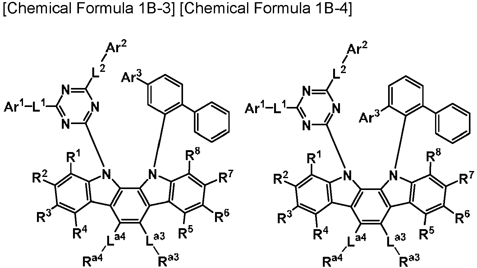 wherein, in Chemical Formula 1B-1 to Chemical Formula 1B-4,Ar1 to Ar3, L1, L2, La3, La4, and R1 to R8 are the same as defined in claim 2.
 - The compound of claim 1, wherein Ar3 is a substituted or unsubstituted phenyl group, a substituted or unsubstituted biphenyl group, a substituted or unsubstituted terphenyl group, a substituted or unsubstituted naphthyl group, a substituted or unsubstituted anthracenyl group, a substituted or unsubstituted phenanthrenyl group, or a substituted or unsubstituted triphenylene group.
- The compound of claim 1, wherein Ar1 and Ar2 are each independently a substituted or unsubstituted phenyl group, a substituted or unsubstituted biphenyl group, a substituted or unsubstituted terphenyl group, a substituted or unsubstituted naphthyl group, a substituted or unsubstituted anthracenyl group, a substituted or unsubstituted phenanthrenyl group, a substituted or unsubstituted triphenylene group, a substituted or unsubstituted fluorenyl group, a substituted or unsubstituted dibenzofuranyl group, a substituted or unsubstituted dibenzothiophenyl group, or a substituted or unsubstituted dibenzosilolyl group.
- The compound of claim 1, wherein -L1-Ar1 and -L2-Ar2 are each independently selected from substituents of Group I :

- The compound of claim 1, which is one of compounds of Group 1:


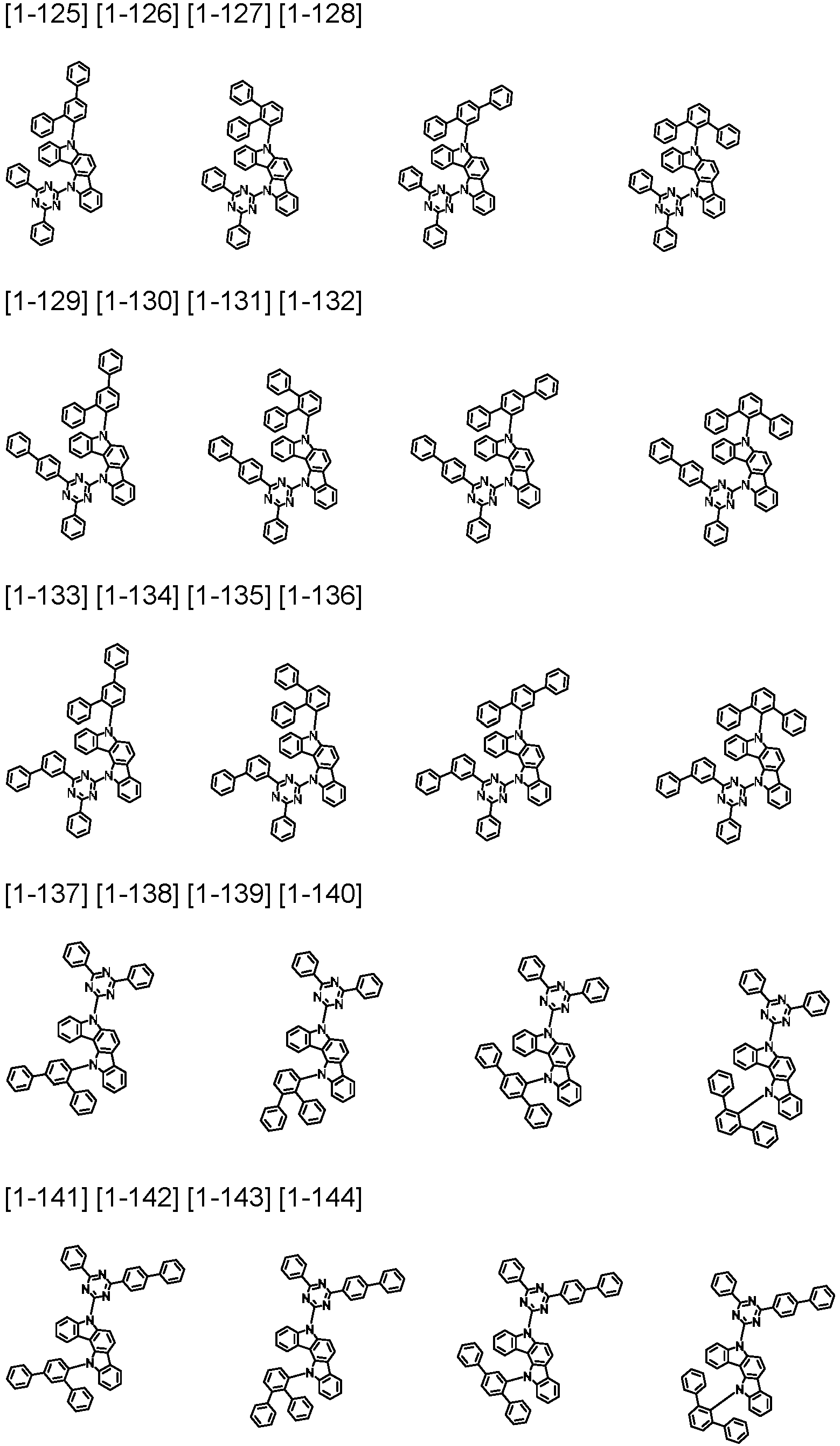


- A composition for an organic optoelectronic device, comprisinga first compound and a second compound,wherein the first compound is the compound for an organic optoelectronic device of claim 1, andthe second compound is a compound for an organic optoelectronic device represented by Chemical Formula 3; or a compound for an organic optoelectronic device represented by a combination of Chemical Formula 4 and Chemical Formula 5:
 wherein, in Chemical Formula 3,Ar4 and Ar5 are each independently a substituted or unsubstituted C6 to C20 aryl group or a substituted or unsubstituted C2 to C30 heterocyclic group,L3 and L4 are each independently a single bond or a substituted or unsubstituted C6 to C20 arylene group,Rb and R9 to R18 are each independently hydrogen, deuterium, a cyano group, a halogen, a substituted or unsubstituted amino group, a substituted or unsubstituted C1 to C30 alkyl group, a substituted or unsubstituted C6 to C30 aryl group, or a substituted or unsubstituted C2 to C30 heterocyclic group, andm is an integer of 0 to 2;
 wherein, in Chemical Formulas 4 and 5,Ar6 and Ar7 are each independently a substituted or unsubstituted C6 to C20 aryl group or a substituted or unsubstituted C2 to C30 heterocyclic group,adjacent two of b1* to b4* of Chemical Formula 4 are each independently linking carbon linked to * in Chemical Formula 5,the rest two of b1* to b4* of Chemical Formula 4 not linked to * in Chemical Formula 5 are each independently C-Lb-Rc,Lb, L5, and L6 are each independently a single bond or a substituted or unsubstituted C6 to C20 arylene group, andRc and R19 to R26 are each independently hydrogen, deuterium, a cyano group, a halogen, a substituted or unsubstituted amino group, a substituted or unsubstituted C1 to C30 alkyl group, a substituted or unsubstituted C6 to C30 aryl group, or a substituted or unsubstituted C2 to C30 heterocyclic group.
 - The composition of claim 8, wherein Chemical Formula 3 is represented by Chemical Formula 3-8:

 R9 to R18 are each independently hydrogen, or a substituted or unsubstituted C6 to C12 aryl group, and-L3-Ar4 and -L4-Ar5 are each independently one of substituents of Group II,
 wherein, in Group II, * is a linking point.
 - The composition of claim 8, wherein the combination of Chemical Formula 4 and Chemical Formula 5 is represented by Chemical Formula 4C:
 Lb3 and Lb4 are a single bond,L5 and L6 are each independently a single bond or a substituted or unsubstituted C6 to C12 arylene group,R19 to R26, Rc3, and Rc4 are each independently hydrogen or a C6 to C12 aryl group, andAr6 and Ar7 are each independently a substituted or unsubstituted phenyl group, a substituted or unsubstituted naphthyl group or a substituted or unsubstituted biphenyl group.
 - An organic optoelectronic device, comprisingan anode and a cathode facing each other,at least one organic layer between the anode and the cathode,wherein the at least one organic layer comprises the compound for an organic optoelectronic device of any one of claim 1 to claim 7; or the composition for an organic optoelectronic device of any one of claim 8 to claim 10.
- The organic optoelectronic device of claim 11, whereinthe at least one organic layer comprises a light emitting layer, andthe light emitting layer comprises the compound for an organic optoelectronic device or the composition for an organic optoelectronic device.
- A display device comprising the organic optoelectronic device of claim 11.
Applications Claiming Priority (2)
| Application Number | Priority Date | Filing Date | Title |
|---|---|---|---|
| KR1020200187970A KR20220095942A (en) | 2020-12-30 | 2020-12-30 | Compound for organic optoelectronic device, composition for organic optoelectronic device, organic optoelectronic device and display device |
| PCT/KR2021/020118 WO2022146011A1 (en) | 2020-12-30 | 2021-12-29 | Compound for organic optoelectronic element, composition for organic optoelectronic element, organic optoelectronic element, and display device |
Publications (2)
| Publication Number | Publication Date |
|---|---|
| EP4273148A1 true EP4273148A1 (en) | 2023-11-08 |
| EP4273148A4 EP4273148A4 (en) | 2024-11-20 |
Family
ID=82260738
Family Applications (1)
| Application Number | Title | Priority Date | Filing Date |
|---|---|---|---|
| EP21915809.4A Pending EP4273148A4 (en) | 2020-12-30 | 2021-12-29 | COMPOUND FOR ORGANIC OPTOELECTRONIC ELEMENT, COMPOSITION FOR ORGANIC OPTOELECTRONIC ELEMENT, ORGANIC OPTOELECTRONIC ELEMENT AND DISPLAY DEVICE |
Country Status (7)
| Country | Link |
|---|---|
| US (1) | US20230212173A1 (en) |
| EP (1) | EP4273148A4 (en) |
| JP (1) | JP7566138B2 (en) |
| KR (2) | KR20220095942A (en) |
| CN (1) | CN116264876A (en) |
| TW (1) | TWI824366B (en) |
| WO (1) | WO2022146011A1 (en) |
Families Citing this family (4)
| Publication number | Priority date | Publication date | Assignee | Title |
|---|---|---|---|---|
| CN115368293B (en) * | 2021-05-18 | 2025-05-16 | 三星Sdi株式会社 | Compound for organic photoelectric device, composition for organic photoelectric device, organic photoelectric device and display device |
| JPWO2023008501A1 (en) * | 2021-07-30 | 2023-02-02 | ||
| WO2024147320A1 (en) | 2023-01-06 | 2024-07-11 | 日鉄ケミカル&マテリアル株式会社 | Organic electroluminescent element |
| WO2025047570A1 (en) * | 2023-08-29 | 2025-03-06 | 日鉄ケミカル&マテリアル株式会社 | Organic electroluminescent element mixed material and organic electroluminescent element |
Family Cites Families (14)
| Publication number | Priority date | Publication date | Assignee | Title |
|---|---|---|---|---|
| US5061569A (en) | 1990-07-26 | 1991-10-29 | Eastman Kodak Company | Electroluminescent device with organic electroluminescent medium |
| JP3065125B2 (en) | 1991-07-03 | 2000-07-12 | 三井化学株式会社 | Organic electroluminescent device |
| JP3295088B2 (en) | 1993-09-29 | 2002-06-24 | 出光興産株式会社 | Organic electroluminescence device |
| JP3194657B2 (en) | 1993-11-01 | 2001-07-30 | 松下電器産業株式会社 | EL device |
| JPH1095973A (en) | 1996-07-24 | 1998-04-14 | Mitsui Petrochem Ind Ltd | Luminescent compound for traveling control and traveling control method using the compound |
| KR102304715B1 (en) * | 2013-06-14 | 2021-09-27 | 삼성디스플레이 주식회사 | Organic light emitting diode |
| KR102577274B1 (en) * | 2015-11-16 | 2023-09-12 | 삼성전자주식회사 | Organic light emitting device |
| KR102171076B1 (en) | 2018-03-21 | 2020-10-28 | 삼성에스디아이 주식회사 | Composition for organic optoelectric device and organic optoelectric device and display device |
| KR20190138378A (en) * | 2018-06-05 | 2019-12-13 | 롬엔드하스전자재료코리아유한회사 | Organic electroluminescent compound and organic electroluminescent device comprising the same |
| KR102408435B1 (en) * | 2019-01-08 | 2022-06-10 | 삼성에스디아이 주식회사 | Compound for organic optoelectronic device, composition for organic optoelectronic device and organic optoelectronic device and display device |
| JP7426382B2 (en) * | 2019-04-25 | 2024-02-01 | 日鉄ケミカル&マテリアル株式会社 | organic electroluminescent device |
| CN110776513B (en) * | 2019-11-29 | 2022-09-27 | 烟台显华化工科技有限公司 | A class of organic compounds and their applications |
| KR102193015B1 (en) * | 2020-03-11 | 2020-12-18 | 주식회사 엘지화학 | Organic light emitting device |
| US12501829B2 (en) * | 2020-11-04 | 2025-12-16 | Samsung Sdi Co., Ltd. | Compound for organic optoelectronic device, composition for organic optoelectronic device, organic optoelectronic device, and display device |
-
2020
- 2020-12-30 KR KR1020200187970A patent/KR20220095942A/en not_active Ceased
-
2021
- 2021-12-29 JP JP2023511975A patent/JP7566138B2/en active Active
- 2021-12-29 US US18/020,478 patent/US20230212173A1/en active Pending
- 2021-12-29 CN CN202180064668.0A patent/CN116264876A/en active Pending
- 2021-12-29 WO PCT/KR2021/020118 patent/WO2022146011A1/en not_active Ceased
- 2021-12-29 TW TW110149436A patent/TWI824366B/en active
- 2021-12-29 EP EP21915809.4A patent/EP4273148A4/en active Pending
-
2025
- 2025-03-31 KR KR1020250041478A patent/KR20250050816A/en active Pending
Also Published As
| Publication number | Publication date |
|---|---|
| EP4273148A4 (en) | 2024-11-20 |
| CN116264876A (en) | 2023-06-16 |
| KR20250050816A (en) | 2025-04-15 |
| JP2023539094A (en) | 2023-09-13 |
| TW202225145A (en) | 2022-07-01 |
| TWI824366B (en) | 2023-12-01 |
| US20230212173A1 (en) | 2023-07-06 |
| JP7566138B2 (en) | 2024-10-11 |
| KR20220095942A (en) | 2022-07-07 |
| WO2022146011A1 (en) | 2022-07-07 |
Similar Documents
| Publication | Publication Date | Title |
|---|---|---|
| EP3901148B1 (en) | Compound for organic optoelectronic element, composition for organic optoelectronic element and organic optoelectronic element and display device | |
| EP4212517B1 (en) | Compound for organic optoelectronic element, composition for organic optoelectronic element, organic optoelectronic element, and display device | |
| EP3575296B1 (en) | Triazine compound, composition and organic optoelectronic device and display device | |
| EP3664172B1 (en) | Compound for organic optoelectronic diode, organic optoelectronic diode, and display device | |
| EP3480278B1 (en) | Compound for organic optoelectronic device, composition for organic optoelectronic device, organic optoelectronic device and display apparatus | |
| EP3480277B1 (en) | Compound for organic optoelectronic device, composition for organic optoelectronic device, organic optoelectronic device and display apparatus | |
| EP3032606A1 (en) | Organic optoelectric device and display device | |
| EP3486299A1 (en) | Compound for organic optoelectronic device, composition for organic optoelectronic device, organic optoelectronic device, and display device | |
| EP3272833A1 (en) | Composition for organic photoelectronic element, organic photoelectronic element, and display apparatus | |
| EP2876104B1 (en) | Polycyclic compound and organic electronic device comprising same | |
| CN110003127B (en) | Composition, organic optoelectronic device and display device | |
| EP3992190A1 (en) | Compound for organic optoelectronic diode, composition for organic optoelectronic diode, organic optoelectronic diode, and display device | |
| US20230212173A1 (en) | Compound for organic optoelectronic element, composition for organic optoelectronic element, organic optoelectronic element, and display device | |
| CN114079026B (en) | Composition for organic photoelectric device, organic photoelectric device and display device | |
| KR102586097B1 (en) | Compound for organic optoelectronic device, organic optoelectronic device and display device | |
| EP3660012B1 (en) | Compound for organic optoelectronic device and organic optoelectronic device and display device | |
| US12213378B2 (en) | Compound for organic optoelectronic device, organic optoelectronic device, and display device | |
| CN120965695A (en) | Compounds, compositions, organic optoelectronic devices and display devices | |
| KR101926022B1 (en) | Organic compound and organic optoelectronic device and display device | |
| CN114464744B (en) | Composition for organic optoelectronic device, organic optoelectronic device and display device | |
| CN113637012B (en) | Compound for organic photoelectric device, composition for organic photoelectric device, organic photoelectric device and display device | |
| KR102599003B1 (en) | Composition for organic optoelectronic device, organic optoelectronic device and display device | |
| CN112368853B (en) | Compound for organic optoelectronic element, composition for organic optoelectronic element, organic optoelectronic element and display device | |
| KR102262471B1 (en) | Composition and organic optoelectronic device and display device | |
| CN113889585B (en) | Composition for organic optoelectronic device, organic optoelectronic device and display device |
Legal Events
| Date | Code | Title | Description |
|---|---|---|---|
| STAA | Information on the status of an ep patent application or granted ep patent |
Free format text: STATUS: THE INTERNATIONAL PUBLICATION HAS BEEN MADE |
|
| PUAI | Public reference made under article 153(3) epc to a published international application that has entered the european phase |
Free format text: ORIGINAL CODE: 0009012 |
|
| STAA | Information on the status of an ep patent application or granted ep patent |
Free format text: STATUS: REQUEST FOR EXAMINATION WAS MADE |
|
| 17P | Request for examination filed |
Effective date: 20230725 |
|
| AK | Designated contracting states |
Kind code of ref document: A1 Designated state(s): AL AT BE BG CH CY CZ DE DK EE ES FI FR GB GR HR HU IE IS IT LI LT LU LV MC MK MT NL NO PL PT RO RS SE SI SK SM TR |
|
| DAV | Request for validation of the european patent (deleted) | ||
| DAX | Request for extension of the european patent (deleted) | ||
| TPAC | Observations filed by third parties |
Free format text: ORIGINAL CODE: EPIDOSNTIPA |
|
| A4 | Supplementary search report drawn up and despatched |
Effective date: 20241023 |
|
| RIC1 | Information provided on ipc code assigned before grant |
Ipc: H10K 101/00 20230101ALN20241017BHEP Ipc: H10K 101/10 20230101ALN20241017BHEP Ipc: H10K 50/11 20230101ALN20241017BHEP Ipc: C07D 307/91 20060101ALI20241017BHEP Ipc: H10K 85/60 20230101ALI20241017BHEP Ipc: C07D 487/04 20060101AFI20241017BHEP |