EP4270674A1 - Isolation component for a tightly packaged high speed connector - Google Patents
Isolation component for a tightly packaged high speed connector Download PDFInfo
- Publication number
- EP4270674A1 EP4270674A1 EP23170513.8A EP23170513A EP4270674A1 EP 4270674 A1 EP4270674 A1 EP 4270674A1 EP 23170513 A EP23170513 A EP 23170513A EP 4270674 A1 EP4270674 A1 EP 4270674A1
- Authority
- EP
- European Patent Office
- Prior art keywords
- assembly
- shield member
- mating
- recited
- shell housing
- Prior art date
- Legal status (The legal status is an assumption and is not a legal conclusion. Google has not performed a legal analysis and makes no representation as to the accuracy of the status listed.)
- Pending
Links
Images


Classifications
-
- H—ELECTRICITY
- H01—ELECTRIC ELEMENTS
- H01R—ELECTRICALLY-CONDUCTIVE CONNECTIONS; STRUCTURAL ASSOCIATIONS OF A PLURALITY OF MUTUALLY-INSULATED ELECTRICAL CONNECTING ELEMENTS; COUPLING DEVICES; CURRENT COLLECTORS
- H01R13/00—Details of coupling devices of the kinds covered by groups H01R12/70 or H01R24/00 - H01R33/00
- H01R13/648—Protective earth or shield arrangements on coupling devices, e.g. anti-static shielding
- H01R13/658—High frequency shielding arrangements, e.g. against EMI [Electro-Magnetic Interference] or EMP [Electro-Magnetic Pulse]
- H01R13/6591—Specific features or arrangements of connection of shield to conductive members
- H01R13/6592—Specific features or arrangements of connection of shield to conductive members the conductive member being a shielded cable
-
- H—ELECTRICITY
- H01—ELECTRIC ELEMENTS
- H01R—ELECTRICALLY-CONDUCTIVE CONNECTIONS; STRUCTURAL ASSOCIATIONS OF A PLURALITY OF MUTUALLY-INSULATED ELECTRICAL CONNECTING ELEMENTS; COUPLING DEVICES; CURRENT COLLECTORS
- H01R13/00—Details of coupling devices of the kinds covered by groups H01R12/70 or H01R24/00 - H01R33/00
- H01R13/648—Protective earth or shield arrangements on coupling devices, e.g. anti-static shielding
- H01R13/658—High frequency shielding arrangements, e.g. against EMI [Electro-Magnetic Interference] or EMP [Electro-Magnetic Pulse]
- H01R13/6581—Shield structure
-
- H—ELECTRICITY
- H01—ELECTRIC ELEMENTS
- H01R—ELECTRICALLY-CONDUCTIVE CONNECTIONS; STRUCTURAL ASSOCIATIONS OF A PLURALITY OF MUTUALLY-INSULATED ELECTRICAL CONNECTING ELEMENTS; COUPLING DEVICES; CURRENT COLLECTORS
- H01R13/00—Details of coupling devices of the kinds covered by groups H01R12/70 or H01R24/00 - H01R33/00
- H01R13/46—Bases; Cases
-
- H—ELECTRICITY
- H01—ELECTRIC ELEMENTS
- H01R—ELECTRICALLY-CONDUCTIVE CONNECTIONS; STRUCTURAL ASSOCIATIONS OF A PLURALITY OF MUTUALLY-INSULATED ELECTRICAL CONNECTING ELEMENTS; COUPLING DEVICES; CURRENT COLLECTORS
- H01R13/00—Details of coupling devices of the kinds covered by groups H01R12/70 or H01R24/00 - H01R33/00
- H01R13/646—Details of coupling devices of the kinds covered by groups H01R12/70 or H01R24/00 - H01R33/00 specially adapted for high-frequency, e.g. structures providing an impedance match or phase match
- H01R13/6461—Means for preventing cross-talk
- H01R13/6463—Means for preventing cross-talk using twisted pairs of wires
-
- H—ELECTRICITY
- H01—ELECTRIC ELEMENTS
- H01R—ELECTRICALLY-CONDUCTIVE CONNECTIONS; STRUCTURAL ASSOCIATIONS OF A PLURALITY OF MUTUALLY-INSULATED ELECTRICAL CONNECTING ELEMENTS; COUPLING DEVICES; CURRENT COLLECTORS
- H01R13/00—Details of coupling devices of the kinds covered by groups H01R12/70 or H01R24/00 - H01R33/00
- H01R13/648—Protective earth or shield arrangements on coupling devices, e.g. anti-static shielding
- H01R13/658—High frequency shielding arrangements, e.g. against EMI [Electro-Magnetic Interference] or EMP [Electro-Magnetic Pulse]
- H01R13/6581—Shield structure
- H01R13/659—Shield structure with plural ports for distinct connectors
-
- H—ELECTRICITY
- H01—ELECTRIC ELEMENTS
- H01R—ELECTRICALLY-CONDUCTIVE CONNECTIONS; STRUCTURAL ASSOCIATIONS OF A PLURALITY OF MUTUALLY-INSULATED ELECTRICAL CONNECTING ELEMENTS; COUPLING DEVICES; CURRENT COLLECTORS
- H01R24/00—Two-part coupling devices, or either of their cooperating parts, characterised by their overall structure
- H01R24/86—Parallel contacts arranged about a common axis
Definitions
- the present invention relates to a high speed, tightly packaged electrical connector.
- the invention is directed to a preassembled nonconductive spacer which optimizes the positioning of the high speed signal contacts in the connector shell.
- isolation component for a tightly packaged high speed connector which enhances the signal integrity (SI) performance of the signal contacts. It would be advantageous to provide an isolation component which can be preassembled to the shell of the connector prior to shipping the connector shell to the customer.
- SI signal integrity
- the solution is provided by an assembly for terminating a high speed cable.
- the assembly includes a shell housing having a mating end and a conductor receiving end.
- a mating portion extends from the mating end.
- the mating portion has a contact receiving opening with an inside wall which extends circumferentially around the opening.
- a crosstalk shield is provided in the shell housing.
- Contacts are positioned in the contact receiving opening of the housing. The contacts terminate high speed conductors of the high speed cable.
- a nonconductive component is provided on the inside wall in the mating portion of the shell housing. The nonconductive component electrically and physically isolates the contacts from the shell housing.
- An object of the present invention is to install a thin, nonconductive layer or component inside a conductive shell of a high speed connector in a mating area where the contacts are oriented very close to the conductive shell (mating area).
- the thin, nonconductive layer or component allows optimal spacing to be maintained while preventing high voltage failures.
- An object of the present invention is to preassemble the nonconductive component in the conductive subassembly so that customers will not have to assemble it themselves, saving time and maintaining performance.
- the thin, nonconductive layer may be in many forms.
- a thin layer of Kapton tape may be applied and fixed to the inner diameter of the affected area.
- a molded component could be installed and trapped inside the shell.
- the relevant inner diameter or surface of the shell has a nonconductive surface treatment applied to achieve the isolating affect.
- An embodiment is directed to an assembly for terminating a high speed cable.
- the assembly includes a shell housing having a mating end and a conductor receiving end.
- a mating portion extends from the mating end.
- the mating portion has a contact receiving opening with an inside wall which extends circumferentially around the opening.
- a crosstalk shield is provided in the shell housing.
- Contacts are positioned in the contact receiving opening of the housing. The contacts terminate high speed conductors of the high speed cable.
- a nonconductive component is provided on the inside wall in the mating portion of the shell housing. The nonconductive component electrically and physically isolates the contacts from the shell housing.
- An embodiment is directed to an assembly for terminating a high speed cable.
- the assembly includes a shell housing with a mating end and a conductor receiving end, with a mating portion extending from the mating end.
- the mating portion has a contact receiving opening with an inside wall which extends circumferentially around the opening.
- a crosstalk shield is provided in the shell housing.
- the crosstalk shield has a first shield member and a second shield member which define contact receiving cavities.
- the first shield member and the second shield member have mounting sections and mating sections, the mating sections are positioned in the mating portion of the shell housing.
- Contacts are positioned in contact spacers in contact receiving cavities in the contact receiving opening of the housing.
- the contacts terminate high speed conductors of the high speed cable.
- the contact receiving cavities are defined by the first shield member and the second shield member of the crosstalk shield.
- a nonconductive component is provided on the inside wall in the mating portion of the shell housing. The nonconductive component electrically and physically isolates the contacts from the
- an electrical connector assembly 10 has a shell housing 12 and a crosstalk shield 14.
- the connector assembly 10 may be a plug connector assembly or a receptacle connector assembly.
- the shell housing 12 has a mating end 20 and a conductor receiving end 22.
- the shell housing 12 has a mating portion 24 proximate the mating end 20.
- the mating portion 24 has a smaller outside diameter D1 than the remainder of the shell housing 12.
- the mating portion 24 has a contact receiving opening 23 with an inner or inside wall 25 which extends circumferentially around the opening 23.
- other configurations of the shell housing 12 may be used.
- a recessed portion 26 is provided on the shell housing 12 proximate the conductor receiving end 22.
- the recessed portion 26 has multiple projections 28 which extend from the surface thereof.
- the recessed portion 26 has an outer diameter of D2, which is larger than the outside diameter D1 of the mating portion 24.
- a shoulder 30 extends circumferentially around the conductor receiving end 22 of the shell housing 12. The shoulder 30 is provided at one end of the recess portion 26.
- other configurations of the shell housing 12 may be used.
- Crosstalk shield receiving recesses or slots 32 extend from the conductor receiving end 22 toward the mating end 20.
- the crosstalk shield receiving slots 32 extend through the shoulder 30 and into the recessed portion 26.
- four crosstalk shield receiving slots 32 are provided to accommodate the configuration of the crosstalk shield 14.
- other numbers of crosstalk shield receiving slots 32 may be used to accommodate different configurations of the crosstalk shield 14.
- the crosstalk shield 14 has a first shield member 40 and a second shield member 42.
- the first shield member 40 and the second shield member 42 are made from nickel silver material, however, other materials, including corrosion resistant materials, may be used which exhibit the shielding characteristics required.
- the first shield member 40 and the second shield member 42 have mounting sections 41 and mating sections 43.
- the width W1 of the mating sections 43 are smaller than the width W2 of the mounting sections 41.
- the mating sections 43 are positioned in the mating portion 24 of the shell housing 12.
- the first shield member 40 and the second shield member 42 have one or more first projections or embossments 52 and one or more second projections or embossments 54 which extend from side edges 56 of the mounting sections 41.
- the first embossments 52 extend from side edges 56 of the first shield member 40 and the second shield member 42 in a direction which is essentially perpendicular to the longitudinal axis of the first shield member 40 and the second shield member 42.
- the second embossments 54 extend from side edges 56 of the first portion 44 in a direction which is essentially perpendicular to the longitudinal axis of the first shield member 40 and the second shield member 42, and in a direction opposite from the first embossments 52.
- the mating sections 43 of the first shield member 40 and the second shield member 42 have side edges 57.
- the width W1 of the mating sections 43 is less than the inside diameter D3 of the contact receiving opening 23 of the mating portion 24 of the connector shell housing 12. Consequently, the side edges 57 of the mating sections 43 of the first shield member 40 and the second shield member 42 are spaced from the inside wall 25 of the mating portion 24.
- the difference between the distance D3 and distance W1 will be sized to suit the voltage the dielectric properties of the components. In one illustrative embodiment, the difference between the distance D3 and distance W1 is between approximately 0.1 mm to approximately 0.5 mm, and preferably between approximately 0.15 mm to approximately 0.3 mm.
- the connector assembly 10 including the shell housing 12 and the crosstalk shield 14 are illustrative. Other types and configurations of the connector assembly 10 may be used.
- a high speed cable 60 with differential pairs of signal conductors 61 is terminated to the shield housing 12 of the connector assembly 10.
- the signal conductors 61 have contacts 63 terminated thereto.
- four pairs, or eight contacts 63 are shown.
- Each of the differential pairs of contacts 63 are positioned in contact insulators or spacers 65 and the contact insulators 65 are positioned in the contact receiving cavities 53 defined by the first shield member 40 and the second shield member 42 of the crosstalk shield 14.
- Each contact spacer 65 houses two contacts 63.
- the contact spacers 65 have a triangular configuration with a first closed side 66, a second closed side 68 and a third open side 70.
- first closed side 66 and the second closed side 68 are positioned proximate the first shield member 40 and the second shield member 42.
- the open third side 70 is positioned proximate the inside wall 25 of the mating portion 24. The open third side 70 is necessitated to allow the contacts 63 to be properly inserted into the contact spacers 65.
- a thin, nonconductive, insulative layer or component 72 is provided in the contact receiving opening 23 of the mating portion 24 of the shell housing 12.
- the thin, nonconductive component 72 may be in many forms.
- a thin layer of Kapton tape may be applied and fixed to the inside wall 25.
- a molded component could be installed and trapped inside the mating portion 24 of the shell housing 12.
- the inside wall 25 of the mating portion 24 may have a nonconductive surface treatment applied thereto to achieve the isolating affect.
- the thin, nonconductive, insulative component 72 may be maintained in the contact receiving opening 23 of the mating portion 24 by adhesive, frictional engagement, bonding or other known methods and may comprise a continuous annular component.
- the thin, nonconductive component 72 has a generally uniform thickness of between approximately 0.1 mm to approximately 0.5 mm, and preferably between approximately 0.15 mm to approximately 0.25 mm. The thickness of the thin, nonconductive component 72 is sufficient to isolate the contacts 63 from the metallic shell housing 12.
- the thin, nonconductive component 72 has recesses 74 spaced periodically about the inner circumferences of the component 72.
- the recesses 74 are positioned to be aligned with the side edges 57 of the mating sections 43 of the first shield member 40 and the second shield member 42.
- the recesses 74 are of reduced cross section as compared to the remainder of the thin, nonconductive component 72.
- the reduced cross section provides clearance for the side edges 57 of the mating sections 43, allowing the reminder of the thin, nonconductive component 72 to have sufficient thickness to isolate the contacts 63 from the metallic shell housing 12.
- the spacing of the side edges 57 from the inside wall 25 is sufficient to allow the positioning of the thin, nonconductive component 72 without the need for recesses 74.
- the contacts 63 must be situated in such a way that leaves very short creepage and clearance distances with relation to the conductive shell housing 12. Without proper isolation, the proximity of the contacts 63 to the conductive shell housing 12 could cause a short circuit failure during irregular high voltage scenarios.
- the thin, nonconductive component 72 of the present invention allows the contacts 63 to be inserted and remain in close proximity to the inside wall 25 of the conductive shell housing 12 while preventing or minimizing the change of a short circuit failure.
- the thin, nonconductive component 72 is positively retained in the contact receiving opening 23 of the mating portion 24 by adhesive, frictional engagement, bonding or other known methods. Consequently, the thin, nonconductive component 72 is assembled to the shell housing 12 during manufacturing of the connector assembly 10, rather than in the field where the assembly is currently done.
Landscapes
- Details Of Connecting Devices For Male And Female Coupling (AREA)
Abstract
Description
- The present invention relates to a high speed, tightly packaged electrical connector. In particular, the invention is directed to a preassembled nonconductive spacer which optimizes the positioning of the high speed signal contacts in the connector shell.
- As high speed connectors become more compact, the spacing in the connector shell must be properly configured to optimize performance. However, existing high speed contacts are not able to maintain a contact pitch for optimal signal integrity (SI) performance, causing the connector shell to be larger than needed or the signal integrity to be diminished. To achieve better spacing and voltage integrity, various connectors require the insertion of a nonconductive spacer to be inserted into the shell after the contacts have been terminated and positioned in the shell of the connector.
- Although adding an appropriate spacer after the contacts have been positioned in the shell of the connector may provide desired signal integrity, the field application of such spacers is difficult and time consuming for the user. Including additional components and sacrificing more signal contacts to maintain spacing will impact connector assembly and performance.
- It is therefore desirable to provide an isolation component for a tightly packaged high speed connector which enhances the signal integrity (SI) performance of the signal contacts. It would be advantageous to provide an isolation component which can be preassembled to the shell of the connector prior to shipping the connector shell to the customer.
- The solution is provided by an assembly for terminating a high speed cable. The assembly includes a shell housing having a mating end and a conductor receiving end. A mating portion extends from the mating end. The mating portion has a contact receiving opening with an inside wall which extends circumferentially around the opening. A crosstalk shield is provided in the shell housing. Contacts are positioned in the contact receiving opening of the housing. The contacts terminate high speed conductors of the high speed cable. A nonconductive component is provided on the inside wall in the mating portion of the shell housing. The nonconductive component electrically and physically isolates the contacts from the shell housing.
- The invention will now be described by way of example with reference to the accompanying drawings in which:
-
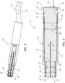
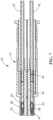
FIG. 1 is a front, side perspective view of an illustrative high speed connector assembly with an illustrative thin, nonconductive layer or component positioned in a mating area of the connector assembly. -
FIG. 2 is a back, side perspective view of the illustrative high speed connector assembly ofFIG. 1 . -
FIG. 3 is a perspective view of the illustrative high speed connector assembly ofFIG. 1 with the contact spacers not shown. -
FIG. 4 is a perspective view of the illustrative high speed connector assembly ofFIG. 1 with the contacts and contact spacers removed and the thin, nonconductive layer or component exploded from the mating end of the connector assembly. -
FIG. 5 is a perspective view of a contact spacer with two contacts positioned therein. -
FIG. 6 is cross-sectional view taken along line 6-6 ofFIG. 1 . -
FIG. 7 is cross-sectional view taken along line 7-7 ofFIG. 1 . - An object of the present invention is to install a thin, nonconductive layer or component inside a conductive shell of a high speed connector in a mating area where the contacts are oriented very close to the conductive shell (mating area). The thin, nonconductive layer or component allows optimal spacing to be maintained while preventing high voltage failures.
- An object of the present invention is to preassemble the nonconductive component in the conductive subassembly so that customers will not have to assemble it themselves, saving time and maintaining performance.
- The thin, nonconductive layer may be in many forms. In one illustrative example, a thin layer of Kapton tape may be applied and fixed to the inner diameter of the affected area. In another illustrative embodiment, a molded component could be installed and trapped inside the shell. In yet another illustrative embodiment, the relevant inner diameter or surface of the shell has a nonconductive surface treatment applied to achieve the isolating affect.
- An embodiment is directed to an assembly for terminating a high speed cable. The assembly includes a shell housing having a mating end and a conductor receiving end. A mating portion extends from the mating end. The mating portion has a contact receiving opening with an inside wall which extends circumferentially around the opening. A crosstalk shield is provided in the shell housing. Contacts are positioned in the contact receiving opening of the housing. The contacts terminate high speed conductors of the high speed cable. A nonconductive component is provided on the inside wall in the mating portion of the shell housing. The nonconductive component electrically and physically isolates the contacts from the shell housing.
- An embodiment is directed to an assembly for terminating a high speed cable. The assembly includes a shell housing with a mating end and a conductor receiving end, with a mating portion extending from the mating end. The mating portion has a contact receiving opening with an inside wall which extends circumferentially around the opening. A crosstalk shield is provided in the shell housing. The crosstalk shield has a first shield member and a second shield member which define contact receiving cavities. The first shield member and the second shield member have mounting sections and mating sections, the mating sections are positioned in the mating portion of the shell housing. Contacts are positioned in contact spacers in contact receiving cavities in the contact receiving opening of the housing. The contacts terminate high speed conductors of the high speed cable. The contact receiving cavities are defined by the first shield member and the second shield member of the crosstalk shield. A nonconductive component is provided on the inside wall in the mating portion of the shell housing. The nonconductive component electrically and physically isolates the contacts from the shell housing.
- As shown in
FIG. 1 , anelectrical connector assembly 10 has ashell housing 12 and acrosstalk shield 14. Theconnector assembly 10 may be a plug connector assembly or a receptacle connector assembly. - The
shell housing 12 has amating end 20 and aconductor receiving end 22. In the illustrative embodiment shown, theshell housing 12 has amating portion 24 proximate themating end 20. Themating portion 24 has a smaller outside diameter D1 than the remainder of theshell housing 12. Themating portion 24 has a contact receiving opening 23 with an inner orinside wall 25 which extends circumferentially around the opening 23. However, other configurations of theshell housing 12 may be used. - A
recessed portion 26 is provided on theshell housing 12 proximate theconductor receiving end 22. Therecessed portion 26 hasmultiple projections 28 which extend from the surface thereof. Therecessed portion 26 has an outer diameter of D2, which is larger than the outside diameter D1 of themating portion 24. Ashoulder 30 extends circumferentially around theconductor receiving end 22 of theshell housing 12. Theshoulder 30 is provided at one end of therecess portion 26. However, other configurations of theshell housing 12 may be used. - Crosstalk shield receiving recesses or
slots 32 extend from theconductor receiving end 22 toward themating end 20. The crosstalkshield receiving slots 32 extend through theshoulder 30 and into the recessedportion 26. In the embodiment shown, four crosstalkshield receiving slots 32 are provided to accommodate the configuration of thecrosstalk shield 14. However, other numbers of crosstalkshield receiving slots 32 may be used to accommodate different configurations of thecrosstalk shield 14. - The
crosstalk shield 14 has afirst shield member 40 and asecond shield member 42. In the illustrative embodiment, thefirst shield member 40 and thesecond shield member 42 are made from nickel silver material, however, other materials, including corrosion resistant materials, may be used which exhibit the shielding characteristics required. - The
first shield member 40 and thesecond shield member 42 have mountingsections 41 andmating sections 43. The width W1 of themating sections 43 are smaller than the width W2 of the mountingsections 41. Themating sections 43 are positioned in themating portion 24 of theshell housing 12. - The
first shield member 40 and thesecond shield member 42 have one or more first projections or embossments 52 and one or more second projections orembossments 54 which extend from side edges 56 of the mountingsections 41. Thefirst embossments 52 extend from side edges 56 of thefirst shield member 40 and thesecond shield member 42 in a direction which is essentially perpendicular to the longitudinal axis of thefirst shield member 40 and thesecond shield member 42. Thesecond embossments 54 extend from side edges 56 of the first portion 44 in a direction which is essentially perpendicular to the longitudinal axis of thefirst shield member 40 and thesecond shield member 42, and in a direction opposite from thefirst embossments 52. - The
mating sections 43 of thefirst shield member 40 and thesecond shield member 42 have side edges 57. The width W1 of themating sections 43 is less than the inside diameter D3 of thecontact receiving opening 23 of themating portion 24 of theconnector shell housing 12. Consequently, the side edges 57 of themating sections 43 of thefirst shield member 40 and thesecond shield member 42 are spaced from theinside wall 25 of themating portion 24. The difference between the distance D3 and distance W1 will be sized to suit the voltage the dielectric properties of the components. In one illustrative embodiment, the difference between the distance D3 and distance W1 is between approximately 0.1 mm to approximately 0.5 mm, and preferably between approximately 0.15 mm to approximately 0.3 mm. - The
connector assembly 10, including theshell housing 12 and thecrosstalk shield 14 are illustrative. Other types and configurations of theconnector assembly 10 may be used. - A
high speed cable 60 with differential pairs ofsignal conductors 61 is terminated to theshield housing 12 of theconnector assembly 10. Thesignal conductors 61 havecontacts 63 terminated thereto. In the illustrative embodiment shown, four pairs, or eightcontacts 63 are shown. Each of the differential pairs ofcontacts 63 are positioned in contact insulators orspacers 65 and thecontact insulators 65 are positioned in thecontact receiving cavities 53 defined by thefirst shield member 40 and thesecond shield member 42 of thecrosstalk shield 14. - Each
contact spacer 65 houses twocontacts 63. The contact spacers 65 have a triangular configuration with a firstclosed side 66, a secondclosed side 68 and a thirdopen side 70. When assembled, the firstclosed side 66 and the secondclosed side 68 are positioned proximate thefirst shield member 40 and thesecond shield member 42. The openthird side 70 is positioned proximate theinside wall 25 of themating portion 24. The openthird side 70 is necessitated to allow thecontacts 63 to be properly inserted into thecontact spacers 65. - A thin, nonconductive, insulative layer or
component 72 is provided in thecontact receiving opening 23 of themating portion 24 of theshell housing 12. The thin,nonconductive component 72 may be in many forms. In one illustrative example, a thin layer of Kapton tape may be applied and fixed to theinside wall 25. In another illustrative embodiment, a molded component could be installed and trapped inside themating portion 24 of theshell housing 12. In yet another illustrative embodiment, theinside wall 25 of themating portion 24 may have a nonconductive surface treatment applied thereto to achieve the isolating affect. - The thin, nonconductive,
insulative component 72 may be maintained in thecontact receiving opening 23 of themating portion 24 by adhesive, frictional engagement, bonding or other known methods and may comprise a continuous annular component. The thin,nonconductive component 72 has a generally uniform thickness of between approximately 0.1 mm to approximately 0.5 mm, and preferably between approximately 0.15 mm to approximately 0.25 mm. The thickness of the thin,nonconductive component 72 is sufficient to isolate thecontacts 63 from themetallic shell housing 12. - In the illustrative embodiment shown, the thin,
nonconductive component 72 hasrecesses 74 spaced periodically about the inner circumferences of thecomponent 72. Therecesses 74 are positioned to be aligned with the side edges 57 of themating sections 43 of thefirst shield member 40 and thesecond shield member 42. In this illustrative embodiment, therecesses 74 are of reduced cross section as compared to the remainder of the thin,nonconductive component 72. The reduced cross section provides clearance for the side edges 57 of themating sections 43, allowing the reminder of the thin,nonconductive component 72 to have sufficient thickness to isolate thecontacts 63 from themetallic shell housing 12. In other embodiments, the spacing of the side edges 57 from theinside wall 25 is sufficient to allow the positioning of the thin,nonconductive component 72 without the need forrecesses 74. - As the size of electrical connector assemblies in general must be reduced to accommodate the small envelopes of the system in which they are installed, it is important to arrange all the components of the
electrical connector assembly 10 in a manner to optimize performance and minimize the overall dimensions of theelectrical connector assembly 10. In particular, thecontacts 63 must be situated in such a way that leaves very short creepage and clearance distances with relation to theconductive shell housing 12. Without proper isolation, the proximity of thecontacts 63 to theconductive shell housing 12 could cause a short circuit failure during irregular high voltage scenarios. The thin,nonconductive component 72 of the present invention allows thecontacts 63 to be inserted and remain in close proximity to theinside wall 25 of theconductive shell housing 12 while preventing or minimizing the change of a short circuit failure. - In the illustrative embodiment shown, the thin,
nonconductive component 72 is positively retained in thecontact receiving opening 23 of themating portion 24 by adhesive, frictional engagement, bonding or other known methods. Consequently, the thin,nonconductive component 72 is assembled to theshell housing 12 during manufacturing of theconnector assembly 10, rather than in the field where the assembly is currently done.
Claims (15)
- An assembly (10) for terminating a high speed cable (60), the assembly (10) comprising:a shell housing (12) having a mating end (20) and a conductor receiving end (22), a mating portion (24) extending from the mating end (20), the mating portion (24) having a contact receiving opening (23) with an inside wall (25) which extends circumferentially around the contact receiving opening (23);a crosstalk shield (14) provided in the shell housing (12);contacts (63) positioned in the contact receiving opening (23) of the housing, the contacts (63) terminating high speed conductors (61) of the high speed cable (60);a nonconductive component (72) provided on the inside wall (25) in the mating portion (24) of the shell housing (12);wherein the nonconductive component (72) electrically and physically isolates the contacts (63) from the shell housing (12).
- The assembly (10) as recited in claim 1, wherein the nonconductive component (72) is a layer of Kapton tape fixed to the inside wall (25).
- The assembly (10) as recited in claim 1, wherein the nonconductive component (72) is a molded component maintained inside the mating portion (24) of the shell housing (12).
- The assembly (10) as recited in claim 1, wherein the nonconductive component (72) is a nonconductive surface treatment applied to the inside wall (25) of the mating portion (24).
- The assembly (10) as recited in any preceding claim, wherein the nonconductive component (72) has a generally uniform thickness of between approximately 0.1 mm to approximately 0.5 mm.
- The assembly (10) as recited in claim 5, wherein the nonconductive component (72) has a thickness of between approximately 0.15 mm to approximately 0.25 mm.
- The assembly (10) as recited in any preceding claim, wherein the crosstalk shield (14) has a first shield member (40) and a second shield member (42) which define contact receiving cavities (53).
- The assembly (10) as recited in any preceding claim, wherein the first shield member (40) and the second shield member (42) have mounting sections (41) and mating sections (43), the mating sections (43) are positioned in the mating portion (24) of the shell housing (12).
- The assembly (10) as recited in claim 8, wherein the mating sections (43) of the first shield member (40) and the second shield member (42) have side edges (57), a width (W1) of the mating sections (43) is less than a diameter (D3) of the contact receiving opening (23) of the mating portion (24) of the connector shell housing (12), wherein the side edges (57) of the mating sections (43) of the first shield member (40) and the second shield member (42) are spaced from the inside wall (25) of the mating portion (24).
- The assembly (10) as recited in claim 9, wherein the side edges (57) of the mating sections (43) of the first shield member (40) and the second shield member (42) are spaced from the inside wall (25) of the mating portion (24) by a distance of between approximately 0.1 mm to approximately 0.5 mm.
- The assembly (10) as recited in claim 9 or 10, wherein the nonconductive component (72) has recesses (74) spaced periodically about an inner circumferences of the nonconductive component (72), the recesses (74) are positioned to be aligned with the side edges (57) of the mating sections (43) of the first shield member (40) and the second shield member (42).
- The assembly (10) as recited in claim 11, wherein the recesses (74) are of reduced cross section as compared to a remainder of the nonconductive component (72), the reduced cross section provides clearance for the side edges (57) of the mating sections (43).
- The assembly (10) as recited in any preceding claim, wherein the contacts (63) are positioned in contact spacers (65).
- The assembly (10) as recited in claim 13, wherein the contact spacers (65) are positioned in the contact receiving cavities (53) defined by the first shield member (40) and the second shield member (42) of the crosstalk shield (14).
- The assembly (10) as recited in claim 13 or 14, wherein each contact spacer (65) houses two contacts (63).
Applications Claiming Priority (1)
| Application Number | Priority Date | Filing Date | Title |
|---|---|---|---|
| US17/732,596 US12244105B2 (en) | 2022-04-29 | 2022-04-29 | Isolation component for a tightly packaged high speed connector |
Publications (1)
| Publication Number | Publication Date |
|---|---|
| EP4270674A1 true EP4270674A1 (en) | 2023-11-01 |
Family
ID=86282589
Family Applications (1)
| Application Number | Title | Priority Date | Filing Date |
|---|---|---|---|
| EP23170513.8A Pending EP4270674A1 (en) | 2022-04-29 | 2023-04-27 | Isolation component for a tightly packaged high speed connector |
Country Status (3)
| Country | Link |
|---|---|
| US (1) | US12244105B2 (en) |
| EP (1) | EP4270674A1 (en) |
| CA (1) | CA3198189A1 (en) |
Families Citing this family (3)
| Publication number | Priority date | Publication date | Assignee | Title |
|---|---|---|---|---|
| US12199385B2 (en) | 2022-04-29 | 2025-01-14 | Te Connectivity Solutions Gmbh | High speed cable braid termination using a coil spring |
| US12266880B2 (en) | 2022-04-29 | 2025-04-01 | Te Connectivity Solutions Gmbh | Contact insulators for use with differential pairs of contacts and method of termination |
| US12244104B2 (en) | 2022-04-29 | 2025-03-04 | Te Connectivity Solutions Gmbh | High speed electrical connector with preassembled EMI shielding |
Citations (5)
| Publication number | Priority date | Publication date | Assignee | Title |
|---|---|---|---|---|
| US20060292927A1 (en) * | 2005-02-18 | 2006-12-28 | Burris Donald A | Sealed tamper resistant terminator |
| US20070099456A1 (en) * | 2005-10-28 | 2007-05-03 | Shawn Chawgo | Protective cap for coaxial cable port terminator |
| DE202010013211U1 (en) * | 2010-12-23 | 2012-03-27 | Weidmüller Interface GmbH & Co. KG | Protection device for electrical connection devices |
| US9257796B1 (en) * | 2015-02-09 | 2016-02-09 | Glenair, Inc. | Electrical connector for high-speed transmission using twisted-pair cable |
| US20200412064A1 (en) * | 2019-06-25 | 2020-12-31 | Itt Manufacturing Enterprises Llc | Crosstalk shield |
Family Cites Families (11)
| Publication number | Priority date | Publication date | Assignee | Title |
|---|---|---|---|---|
| DE102009021594B4 (en) | 2009-04-09 | 2018-04-12 | Phoenix Contact Gmbh & Co. Kg | Electrical connector and electrical connector and method for connecting the remainder of a multicore cable to an electrical connector |
| DE202012008970U1 (en) | 2012-09-18 | 2012-10-17 | Rosenberger Hochfrequenztechnik Gmbh & Co. Kg | Connectors |
| DE202015100245U1 (en) | 2015-01-21 | 2016-02-02 | FILTEC GmbH Filtertechnologie für die Elektronikindustrie | Socket assembly comprising a shielded socket for printed circuit boards or boards |
| DE102015109311B4 (en) | 2015-06-11 | 2017-02-16 | Provertha Connectors, Cables & Solutions Gmbh | Circular connector for data transmission of high data rates |
| US9923285B2 (en) | 2016-06-20 | 2018-03-20 | Richards Manufacturing Company, A New Jersey Limited Partnership | Method and related device for connecting to a metallic shield of a cable |
| DE102019106980B3 (en) | 2019-03-19 | 2020-07-02 | Harting Electric Gmbh & Co. Kg | Contact carriers and connectors for a shielded hybrid contact arrangement |
| WO2021009833A1 (en) | 2019-07-16 | 2021-01-21 | 三菱電機株式会社 | Connector |
| JP7487696B2 (en) * | 2021-03-26 | 2024-05-21 | 住友電装株式会社 | connector |
| US12266880B2 (en) | 2022-04-29 | 2025-04-01 | Te Connectivity Solutions Gmbh | Contact insulators for use with differential pairs of contacts and method of termination |
| US12199385B2 (en) | 2022-04-29 | 2025-01-14 | Te Connectivity Solutions Gmbh | High speed cable braid termination using a coil spring |
| US12244104B2 (en) | 2022-04-29 | 2025-03-04 | Te Connectivity Solutions Gmbh | High speed electrical connector with preassembled EMI shielding |
-
2022
- 2022-04-29 US US17/732,596 patent/US12244105B2/en active Active
-
2023
- 2023-04-27 EP EP23170513.8A patent/EP4270674A1/en active Pending
- 2023-04-28 CA CA3198189A patent/CA3198189A1/en active Pending
Patent Citations (5)
| Publication number | Priority date | Publication date | Assignee | Title |
|---|---|---|---|---|
| US20060292927A1 (en) * | 2005-02-18 | 2006-12-28 | Burris Donald A | Sealed tamper resistant terminator |
| US20070099456A1 (en) * | 2005-10-28 | 2007-05-03 | Shawn Chawgo | Protective cap for coaxial cable port terminator |
| DE202010013211U1 (en) * | 2010-12-23 | 2012-03-27 | Weidmüller Interface GmbH & Co. KG | Protection device for electrical connection devices |
| US9257796B1 (en) * | 2015-02-09 | 2016-02-09 | Glenair, Inc. | Electrical connector for high-speed transmission using twisted-pair cable |
| US20200412064A1 (en) * | 2019-06-25 | 2020-12-31 | Itt Manufacturing Enterprises Llc | Crosstalk shield |
Also Published As
| Publication number | Publication date |
|---|---|
| US12244105B2 (en) | 2025-03-04 |
| CA3198189A1 (en) | 2023-10-29 |
| US20230352883A1 (en) | 2023-11-02 |
Similar Documents
| Publication | Publication Date | Title |
|---|---|---|
| US10699823B2 (en) | Cable assembly for electrical connector | |
| US11901678B2 (en) | Contact member for electrical connector | |
| EP2415128B1 (en) | Coaxial connector with inner shielding arrangement and method of assembling one | |
| CN2462561Y (en) | Low structured miniature coaxial line connector | |
| US8398431B1 (en) | Receptacle assembly | |
| US4516815A (en) | RF filter connector | |
| US12244105B2 (en) | Isolation component for a tightly packaged high speed connector | |
| EP0836248B1 (en) | Impedance matched cable assembly having latching subassembly | |
| US6162086A (en) | Cable end connector having an inner shielding casing capable of securely retaining and grounding a cable therein | |
| CN101010833A (en) | Modular plug assemblies, terminated cable assemblies and methods for forming these assemblies | |
| WO2010119011A1 (en) | Coaxial connector and method of assembling one | |
| JPH07106003A (en) | Modular coaxial cable connector and assembly method thereof | |
| JP5827818B2 (en) | High-speed electrical contact assembly | |
| JP2024533132A5 (en) | ||
| EP4270679A1 (en) | High speed electrical connector with preassembled emi sheilding | |
| WO2023192532A1 (en) | Angled subassembly for an angled connector and method of assembling thereof | |
| US20030176085A1 (en) | Electrical connector assembly | |
| TWI440265B (en) | Coaxial connector and coaxial multipole connector | |
| CN107851938A (en) | Shielded connector and its manufacturing method | |
| JP3425634B2 (en) | Electrical connector with shield termination for high-speed cables | |
| WO2003075411A1 (en) | Connector assembling with side grounding pin | |
| JP3398890B2 (en) | Electrical connector with coaxial cable termination | |
| EP0951092A2 (en) | Electrical connector for coaxial cables | |
| US20240243512A1 (en) | Connector | |
| JP7388264B2 (en) | Connectors and cables with connectors |
Legal Events
| Date | Code | Title | Description |
|---|---|---|---|
| PUAI | Public reference made under article 153(3) epc to a published international application that has entered the european phase |
Free format text: ORIGINAL CODE: 0009012 |
|
| STAA | Information on the status of an ep patent application or granted ep patent |
Free format text: STATUS: THE APPLICATION HAS BEEN PUBLISHED |
|
| AK | Designated contracting states |
Kind code of ref document: A1 Designated state(s): AL AT BE BG CH CY CZ DE DK EE ES FI FR GB GR HR HU IE IS IT LI LT LU LV MC ME MK MT NL NO PL PT RO RS SE SI SK SM TR |
|
| STAA | Information on the status of an ep patent application or granted ep patent |
Free format text: STATUS: REQUEST FOR EXAMINATION WAS MADE |
|
| 17P | Request for examination filed |
Effective date: 20240429 |
|
| RBV | Designated contracting states (corrected) |
Designated state(s): AL AT BE BG CH CY CZ DE DK EE ES FI FR GB GR HR HU IE IS IT LI LT LU LV MC ME MK MT NL NO PL PT RO RS SE SI SK SM TR |
|
| STAA | Information on the status of an ep patent application or granted ep patent |
Free format text: STATUS: EXAMINATION IS IN PROGRESS |
|
| 17Q | First examination report despatched |
Effective date: 20251017 |