EP4270668A1 - Connector - Google Patents
Connector Download PDFInfo
- Publication number
- EP4270668A1 EP4270668A1 EP21910681.2A EP21910681A EP4270668A1 EP 4270668 A1 EP4270668 A1 EP 4270668A1 EP 21910681 A EP21910681 A EP 21910681A EP 4270668 A1 EP4270668 A1 EP 4270668A1
- Authority
- EP
- European Patent Office
- Prior art keywords
- connector
- catching
- contact
- shell
- cover shell
- Prior art date
- Legal status (The legal status is an assumption and is not a legal conclusion. Google has not performed a legal analysis and makes no representation as to the accuracy of the status listed.)
- Pending
Links
Images






Classifications
-
- H—ELECTRICITY
- H01—ELECTRIC ELEMENTS
- H01R—ELECTRICALLY-CONDUCTIVE CONNECTIONS; STRUCTURAL ASSOCIATIONS OF A PLURALITY OF MUTUALLY-INSULATED ELECTRICAL CONNECTING ELEMENTS; COUPLING DEVICES; CURRENT COLLECTORS
- H01R13/00—Details of coupling devices of the kinds covered by groups H01R12/70 or H01R24/00 - H01R33/00
- H01R13/62—Means for facilitating engagement or disengagement of coupling parts or for holding them in engagement
- H01R13/629—Additional means for facilitating engagement or disengagement of coupling parts, e.g. aligning or guiding means, levers, gas pressure electrical locking indicators, manufacturing tolerances
- H01R13/631—Additional means for facilitating engagement or disengagement of coupling parts, e.g. aligning or guiding means, levers, gas pressure electrical locking indicators, manufacturing tolerances for engagement only
-
- H—ELECTRICITY
- H01—ELECTRIC ELEMENTS
- H01R—ELECTRICALLY-CONDUCTIVE CONNECTIONS; STRUCTURAL ASSOCIATIONS OF A PLURALITY OF MUTUALLY-INSULATED ELECTRICAL CONNECTING ELEMENTS; COUPLING DEVICES; CURRENT COLLECTORS
- H01R24/00—Two-part coupling devices, or either of their cooperating parts, characterised by their overall structure
- H01R24/38—Two-part coupling devices, or either of their cooperating parts, characterised by their overall structure having concentrically or coaxially arranged contacts
- H01R24/40—Two-part coupling devices, or either of their cooperating parts, characterised by their overall structure having concentrically or coaxially arranged contacts specially adapted for high frequency
- H01R24/50—Two-part coupling devices, or either of their cooperating parts, characterised by their overall structure having concentrically or coaxially arranged contacts specially adapted for high frequency mounted on a PCB [Printed Circuit Board]
-
- H—ELECTRICITY
- H01—ELECTRIC ELEMENTS
- H01R—ELECTRICALLY-CONDUCTIVE CONNECTIONS; STRUCTURAL ASSOCIATIONS OF A PLURALITY OF MUTUALLY-INSULATED ELECTRICAL CONNECTING ELEMENTS; COUPLING DEVICES; CURRENT COLLECTORS
- H01R12/00—Structural associations of a plurality of mutually-insulated electrical connecting elements, specially adapted for printed circuits, e.g. printed circuit boards [PCB], flat or ribbon cables, or like generally planar structures, e.g. terminal strips, terminal blocks; Coupling devices specially adapted for printed circuits, flat or ribbon cables, or like generally planar structures; Terminals specially adapted for contact with, or insertion into, printed circuits, flat or ribbon cables, or like generally planar structures
- H01R12/70—Coupling devices
- H01R12/71—Coupling devices for rigid printing circuits or like structures
-
- H—ELECTRICITY
- H01—ELECTRIC ELEMENTS
- H01R—ELECTRICALLY-CONDUCTIVE CONNECTIONS; STRUCTURAL ASSOCIATIONS OF A PLURALITY OF MUTUALLY-INSULATED ELECTRICAL CONNECTING ELEMENTS; COUPLING DEVICES; CURRENT COLLECTORS
- H01R12/00—Structural associations of a plurality of mutually-insulated electrical connecting elements, specially adapted for printed circuits, e.g. printed circuit boards [PCB], flat or ribbon cables, or like generally planar structures, e.g. terminal strips, terminal blocks; Coupling devices specially adapted for printed circuits, flat or ribbon cables, or like generally planar structures; Terminals specially adapted for contact with, or insertion into, printed circuits, flat or ribbon cables, or like generally planar structures
- H01R12/70—Coupling devices
- H01R12/71—Coupling devices for rigid printing circuits or like structures
- H01R12/712—Coupling devices for rigid printing circuits or like structures co-operating with the surface of the printed circuit or with a coupling device exclusively provided on the surface of the printed circuit
- H01R12/714—Coupling devices for rigid printing circuits or like structures co-operating with the surface of the printed circuit or with a coupling device exclusively provided on the surface of the printed circuit with contacts abutting directly the printed circuit; Button contacts therefore provided on the printed circuit
-
- H—ELECTRICITY
- H01—ELECTRIC ELEMENTS
- H01R—ELECTRICALLY-CONDUCTIVE CONNECTIONS; STRUCTURAL ASSOCIATIONS OF A PLURALITY OF MUTUALLY-INSULATED ELECTRICAL CONNECTING ELEMENTS; COUPLING DEVICES; CURRENT COLLECTORS
- H01R13/00—Details of coupling devices of the kinds covered by groups H01R12/70 or H01R24/00 - H01R33/00
- H01R13/46—Bases; Cases
- H01R13/502—Bases; Cases composed of different pieces
- H01R13/5025—Bases; Cases composed of different pieces one or more pieces being of resilient material
-
- H—ELECTRICITY
- H01—ELECTRIC ELEMENTS
- H01R—ELECTRICALLY-CONDUCTIVE CONNECTIONS; STRUCTURAL ASSOCIATIONS OF A PLURALITY OF MUTUALLY-INSULATED ELECTRICAL CONNECTING ELEMENTS; COUPLING DEVICES; CURRENT COLLECTORS
- H01R13/00—Details of coupling devices of the kinds covered by groups H01R12/70 or H01R24/00 - H01R33/00
- H01R13/46—Bases; Cases
- H01R13/502—Bases; Cases composed of different pieces
- H01R13/508—Bases; Cases composed of different pieces assembled by a separate clip or spring
-
- H—ELECTRICITY
- H01—ELECTRIC ELEMENTS
- H01R—ELECTRICALLY-CONDUCTIVE CONNECTIONS; STRUCTURAL ASSOCIATIONS OF A PLURALITY OF MUTUALLY-INSULATED ELECTRICAL CONNECTING ELEMENTS; COUPLING DEVICES; CURRENT COLLECTORS
- H01R13/00—Details of coupling devices of the kinds covered by groups H01R12/70 or H01R24/00 - H01R33/00
- H01R13/46—Bases; Cases
- H01R13/533—Bases, cases made for use in extreme conditions, e.g. high temperature, radiation, vibration, corrosive environment, pressure
-
- H—ELECTRICITY
- H01—ELECTRIC ELEMENTS
- H01R—ELECTRICALLY-CONDUCTIVE CONNECTIONS; STRUCTURAL ASSOCIATIONS OF A PLURALITY OF MUTUALLY-INSULATED ELECTRICAL CONNECTING ELEMENTS; COUPLING DEVICES; CURRENT COLLECTORS
- H01R13/00—Details of coupling devices of the kinds covered by groups H01R12/70 or H01R24/00 - H01R33/00
- H01R13/648—Protective earth or shield arrangements on coupling devices, e.g. anti-static shielding
- H01R13/658—High frequency shielding arrangements, e.g. against EMI [Electro-Magnetic Interference] or EMP [Electro-Magnetic Pulse]
-
- H—ELECTRICITY
- H01—ELECTRIC ELEMENTS
- H01R—ELECTRICALLY-CONDUCTIVE CONNECTIONS; STRUCTURAL ASSOCIATIONS OF A PLURALITY OF MUTUALLY-INSULATED ELECTRICAL CONNECTING ELEMENTS; COUPLING DEVICES; CURRENT COLLECTORS
- H01R13/00—Details of coupling devices of the kinds covered by groups H01R12/70 or H01R24/00 - H01R33/00
- H01R13/648—Protective earth or shield arrangements on coupling devices, e.g. anti-static shielding
- H01R13/658—High frequency shielding arrangements, e.g. against EMI [Electro-Magnetic Interference] or EMP [Electro-Magnetic Pulse]
- H01R13/6591—Specific features or arrangements of connection of shield to conductive members
- H01R13/6594—Specific features or arrangements of connection of shield to conductive members the shield being mounted on a PCB and connected to conductive members
- H01R13/6595—Specific features or arrangements of connection of shield to conductive members the shield being mounted on a PCB and connected to conductive members with separate members fixing the shield to the PCB
-
- H—ELECTRICITY
- H01—ELECTRIC ELEMENTS
- H01R—ELECTRICALLY-CONDUCTIVE CONNECTIONS; STRUCTURAL ASSOCIATIONS OF A PLURALITY OF MUTUALLY-INSULATED ELECTRICAL CONNECTING ELEMENTS; COUPLING DEVICES; CURRENT COLLECTORS
- H01R12/00—Structural associations of a plurality of mutually-insulated electrical connecting elements, specially adapted for printed circuits, e.g. printed circuit boards [PCB], flat or ribbon cables, or like generally planar structures, e.g. terminal strips, terminal blocks; Coupling devices specially adapted for printed circuits, flat or ribbon cables, or like generally planar structures; Terminals specially adapted for contact with, or insertion into, printed circuits, flat or ribbon cables, or like generally planar structures
- H01R12/70—Coupling devices
- H01R12/71—Coupling devices for rigid printing circuits or like structures
- H01R12/72—Coupling devices for rigid printing circuits or like structures coupling with the edge of the rigid printed circuits or like structures
- H01R12/722—Coupling devices for rigid printing circuits or like structures coupling with the edge of the rigid printed circuits or like structures coupling devices mounted on the edge of the printed circuits
- H01R12/724—Coupling devices for rigid printing circuits or like structures coupling with the edge of the rigid printed circuits or like structures coupling devices mounted on the edge of the printed circuits containing contact members forming a right angle
-
- H—ELECTRICITY
- H01—ELECTRIC ELEMENTS
- H01R—ELECTRICALLY-CONDUCTIVE CONNECTIONS; STRUCTURAL ASSOCIATIONS OF A PLURALITY OF MUTUALLY-INSULATED ELECTRICAL CONNECTING ELEMENTS; COUPLING DEVICES; CURRENT COLLECTORS
- H01R43/00—Apparatus or processes specially adapted for manufacturing, assembling, maintaining, or repairing of line connectors or current collectors or for joining electric conductors
- H01R43/16—Apparatus or processes specially adapted for manufacturing, assembling, maintaining, or repairing of line connectors or current collectors or for joining electric conductors for manufacturing contact members, e.g. by punching and by bending
Definitions
- the present invention relates to a connector suitable for transmission of a high frequency signal.
- a high frequency signal is susceptible to electromagnetic noises, and, in order to reduce the influence of electromagnetic noises, a connector having a structure covered with a shield is adopted. That is, a connector is employed that has a structure where a contact for directly transmitting a high frequency signal is supported by a housing, and the contact and the housing are enclosed with a shield.
- Patent Literature 1 discloses a connector having a structure where a contact is supported by a housing referred to as an insulator, which in turn is enclosed with shields referred to as an outer peripheral shell and a back shell.
- each of components constituting the connector has its tolerance, namely a dimensional tolerance. Therefore, this dimensional tolerance may cause the transmission characteristics of the connector completed by assembling such components together to vary among the connectors. If this variation is great, the connector has to be handled as having low transmission characteristics according to the great variation, and thus the variation hinders configuring a connector having high-performance transmission characteristics. In order to reduce the dimensional tolerance, each component has to be manufactured with high precision, but pursuing this causes the components to be costly, and is therefore limited.
- An object of the present invention is to provide a connector made less susceptible to a dimensional tolerance of a component by assembly.
- a connector of the present invention that achieves the above object includes:
- the connector of the present invention has a structure where the cover shell includes the contacting portion, the catching portion, and the spring portion, and the catching portion is caught on the grounding portion of the front shell, which causes the spring portion to deform elastically. Therefore, in the connector of the present invention, the elastic deformation of the spring portion, on the one hand, causes the cover shell to contact the front shell while pressing the rear end upper portion of the front shell upward at the contacting portion. This ensures that the cover shell contacts the front shell both at the contacting portion and at the catching portion, thereby ensuring good shielding performance. In addition, on the other hand, the elastic deformation of the spring portion causes this cover shell to contact the back housing while pressing the back housing frontward. This prevents a gap from occurring between the back housing and the cover shell, regardless of a dimensional tolerance of the front housing or the back housing, so that the connector is achieved that is less susceptible to the dimensional tolerance and has high-performance transmission characteristics.
- the front shell have a tongue projecting rearward at the rear end upper portion of the front shell, the contacting portion have a recess receiving the tongue, and the elastic deformation of the spring portion cause the cover shell to press the tongue received in the recess upward.
- the grounding portion have an extending portion extending laterally, and the catching portion catch on the extending portion, thereby causing the spring portion to deform elastically.
- the grounding portion is provided with the extending portion extending laterally, and the catching portion is caught on this extending portion, the catching portion can reliably catch on the grounding portion.
- the catching portion have a depression depressed upward, and catch on the extending portion at the depression.
- the catching portion Since the catching portion has a depressed shape, the catching portion can more reliably catch on the grounding portion.
- the spring portion have a shape projecting more frontward than the catching portion.
- the cover shell can be assigned the action of contacting the back housing while pressing the back housing frontward, and simultaneously contacting the front shell while pressing the rear end upper portion of the front shell upward at the contacting portion.
- the spring portion when the spring portion is provided in such a position as to project more frontward than the catching portion, it is preferred that the spring portion have a hole, and catching of the catching portion cause the elastic deformation accompanied by deformation of the hole.
- the spring force is adjusted, so that the spring portion that performs the above action reliably is formed.
- Figures 1(A) and 1(B) are isometric views of a connector as an embodiment of the present invention.
- Figures 1(A) and 1(B) are isometric views as viewed from different directions.
- Figures 2(A) to 2(E) are diagrams, as viewed in six directions, of the connector shown in isometric views in Figures 1(A) and 1(B) .
- Figures 2(A), 2(B), 2(C), 2(D), and 2(E) are a top view, a front view, a side view, a rear view, and a bottom view, respectively.
- Figure 3 is an exploded isometric view of the connector shown in Figures 1(A) and 1(B) and Figures 2(A) to 2(E) .
- This connector 100 is composed of a front shell 10, a front housing 20, a contact 30, a back housing 40, and a cover shell 50.
- the contact 30 is a component made of a conductor, for example, a copper alloy.
- the conductor constituting this contact 30 is equivalent to an example of a first conductor as referred to in the present invention.
- This contact 30 has a base portion 31, a contact portion 32, and a board connecting portion 33.
- the contact portion 32 extends from the base portion 31 in a frontward direction in which the connector 100 mates with a mating connector (not shown), and makes electrical contact with a mating contact (not shown) provided in the mating connector.
- the contact portion 32 of the contact 30 of the present embodiment is a rod-like horizontally extending male contact portion.
- the board connecting portion 33 extends from the base portion 31 in a downward direction in which a circuit board (not shown) is positioned, and makes connection to the circuit board.
- the board connecting portion 33 of the contact 30 of the present embodiment is of a surface mounting type that is soldered to the surface of the circuit board. That is, this board connecting portion 33 extends downward, and thereafter bends rearward and extends horizontally. This horizontally extending portion is placed on the surface of the circuit board and soldered thereto.
- the front housing 20 is composed of a resin that is an example of a first dielectric as referred to in the present invention.
- a longitudinal through-hole 21 is formed in the front housing 20 of the present embodiment.
- the front housing 20 supports the base portion 31 with the contact portion 32 of the contact 30 inserted through the hole 21 and exposed frontward.
- the back housing 40 is composed of a resin that is an example of a second dielectric as referred to in the present invention.
- This back housing 40 supports the base portion 31 such that the base portion 31 is held between the back housing 40 and the front housing 20, with the board connecting portion 33 exposed downward.
- the front shell 10 is composed of a sheet material made of a conductor such as a copper alloy, and is stamped and formed.
- a conductor such as a copper alloy constituting this front shell 10 is equivalent to an example of a second conductor as referred to in the present invention.
- This front shell 10 has a barrel portion 11 and a grounding portion 12.
- the barrel portion 11 has a longitudinally extending substantially cylindrical shape.
- the contact portion 32 of the contact 30 is inserted into this barrel portion 11, and the barrel portion 11 encloses the contact portion 32 inserted thereinto at a distance from the contact portion 32.
- grounding portion 12 is continuous with a rear portion of the barrel portion 11 and widens downward. This grounding portion 12 makes connection to the circuit board. This grounding portion 12, like the board connecting portion 33 of the contact, also bends rearward halfway and extends horizontally. This horizontally extending portion is placed on the surface of the circuit board and soldered thereto.
- the grounding portion 12 of the present embodiment has such a shape as to be soldered at two right and left locations.
- the cover shell 50 is also composed of a sheet material made of a conductor such as a copper alloy, and is stamped and formed into such a shape as to cover the back housing 40.
- the conductor, such as a copper alloy, constituting this cover shell 50 is equivalent to an example of a third conductor as referred to in the present invention.
- This cover shell 50 is formed with a contacting portion 51, a catching portion 52, and a spring portion 53.
- the contacting portion 51 contacts a rear end upper portion of the front shell 10 from below.
- the rear end upper portion of the front shell 10 is provided with a rearward projecting tongue 13.
- the contacting portion 51 is provided with a recess 511 for receiving the tongue 13. The action of elastic deformation of the spring portion 53, which will be described later, causes this cover shell 50 to press the tongue 13 received in the recess 511 upward, thereby ensuring reliable contact between the front shell 10 and the cover shell 50.
- the catching portion 52 catches on the grounding portion 12 of the front shell 11.
- the grounding portion 12 is provided with an extending portion 121 extending laterally.
- the catching portion 52 has a depression 521 (see Figure 3 and Figure 4(A) ) depressed upward. This depression 521 of the catching portion 52 catches on the extending portion 121 such that it rests astride the extending portion 121.
- the grounding portion 12 is provided with a pair of extending portions 121 extending rightward and leftward, respectively.
- a pair of right and left catching portions 52 are formed, and the cover shell 50 catches on the front shell 10 at the two right and left catching portions 52.
- catching portions 52 catch on the extending portions 121, thereby contacting the front shell 10 reliably. That is, the cover shell 50 contacts the front shell 10 at three locations in total: the contact portion 51 formed at the top; and the pair of right and left catching portions 52 at the bottom, and is kept at the same potential as the front shell 10 to serve as a shield.
- the spring portion 53 elastically deforms.
- the elastic deformation of this spring portion 53 causes the cover shell 50 to press the tongue 13 received in the recess 511 upward, thereby ensuring reliable contact between the front shell 10 and the cover shell 50.
- the elastic deformation of the spring portion 53 causes the cover shell 50 to contact the back housing 40 while pressing the back housing 40 frontward. This prevents formation of a gap between the back housing 40 and the cover housing 50 regardless of a dimensional tolerance of a component such as the back housing 40 or the cover shell 50, thereby reducing variations in the transmission characteristics among the connectors 100.
- the spring portion 53 has a shape projecting more frontward than the catching portion 52.
- This spring portion 53 is also so formed as to be a pair of right and left spring portions.
- a hole 531 is formed in the spring portion 53. Therefore, when the catching portion 52 catches on the extending portion 121, the spring portion 53 undergoes elastic deformation accompanied by deformation of the hole 531.
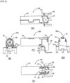
- Figure 4(A) is a side view of this connector, showing a state before the cover shell is assembled
- Figure 4(B) is a side view thereof, showing a state completed by assembling the cover shell
- Figure 4(C) is a partially cross-sectional side view thereof in an assembled state.
- Figure 4(B) is the same diagram as Figure 2(C) with vectorial representation of a force exerted on the extending portion 121 by the cover shell 50.
- the cover shell 50 is a component to be assembled last.
- the tongue 13 of the front shell 10 is received in the recess 511 of the contacting portion 51, and the catching portion 53 is caught on the extending portion 121.
- This vector X is decomposed into a horizontal component Y and a vertical component Z.
- the vertical component Z causes the tongue 13 of the front shell 10 to be pressed upward by the contacting portion 51, thereby ensuring electrical contact between the tongue 13 and the contacting portion 51, and simultaneously ensures that the catching portion 52 catches on the extending portion 121, thereby also ensuring electrical connection between the catching portion 52 and the extending portion 121.
- a reaction force of the horizontal component Y causes the back housing 40 to be pressed from behind by the cover shell 50, thereby preventing creation of a gap between the back housing 40 and the cover shell 50, as indicated by an arrow P in Figure 4(C) , regardless of a dimensional tolerance of a component.
- Figure 5 is an exploded isometric view of a connector as a comparative example.
- This connector 200 of the comparative example shown in Figure 5 is composed of a front shell 10, a front housing 20, a contact 30, a back housing 40, and a cover shell 60. All of these components except for the cover shell 60 are the same as the corresponding components of the connector 100 of the present embodiment shown in Figure 3 .
- the cover shell 60 is different from the cover shell 50 shown in Figure 3 in that it lacks the spring portion 53.
- this cover shell 60 of the comparative example has a structure where lanced tabs 61 are formed on right and left walls to hold the back housing 40 elastically therebetween from the right and left sides.
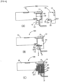
- Figures 6(A) and 6(B) are side views of the connector of the comparative example.
- Figure 6(A) shows the connector 200 with the cover shell 60 in contact with both the tongue 13 and the extending portion 121 of the front shell 10.
- Figure 6(B) because of the fact that the cover shell 60 is shorter in vertical dimension, or the like, a gap has occurred between the cover shell 60 and the extending portion 121, as indicated by an arrow Q.
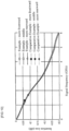
- Figure 7 is a diagram showing voltage standing wave ratio in the comparative example.
- the horizontal axis represents signal frequency (GHz), and the horizontal axis represents voltage standing wave ratio (VSWR).
- the "contact" graph shown in the solid line is a graph when the cover shell 60 is in contact with both the tongue 13 and the extending portion 121 of the front shell 10, as shown in Figure 6(A) .
- the "contactless” graph shown in the dashed line is a graph when the cover shell 60 is in contact with the tongue 13 of the front shell 10 but a gap lies between the cover shell 60 and the extending portion 121, as shown in Figure 6(B) .
- the voltage standing wave ratio (VSWR) keeps its lower values until higher frequencies in the solid line graph.
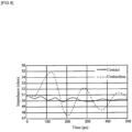
- Figure 8 is a diagram showing impedance in the comparative example.
- the impedance (ohm) is more stable at around 50 ohm in the solid line graph.
- the cover shell 50 is always kept in contact with both the tongue 13 and the extending portion 121 of the front shell 10.
- Figures 9(A) and 9(B) are partially cross-sectional side views of the connector of the comparative example.
- the cover shell 60 is in contact with the back housing 40.
- Figure 9(B) because of the fact that the cover shell 60 is longer in longitudinal dimension, or the like, a gap has occurred between the cover shell 60 and the back housing 40, as indicated by an arrow R.
- Figure 10 is a diagram showing insertion loss in "Example” and “Comparative Example”.
- the horizontal axis represents signal frequency (GHz), and the vertical axis represents insertion loss (dB).
- the "Example” refers to a connector having the structure shown in Figure 3
- the “Comparative Example” refers to a connector having the structure shown in Figure 5
- “more frontward”, “middle”, and “more rearward” mean longitudinal positions of a rear face of the cover shell 50 (or the cover shell 60) after assembly.
- “Comparative Example” when the cover shell 60 is more rearward, it means that a gap has occurred between the cover shell 60 and the back housing 40, as shown in Figure 9(B) .
- the insertion loss (dB) is almost the same between the “Example” and the “Comparative Example”, and also between the “more frontward”, the “middle”, and the “more rearward”.
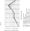
- FIG 11 is a diagram showing voltage standing wave ratio (VSWR) of "Example” and “Comparative Example”.
- the horizontal axis represents signal frequency (GHz), and the vertical axis represents voltage standing wave ratio (VSWR).
- GHz signal frequency
- VSWR voltage standing wave ratio
- Figure 12 is a diagram showing impedance (ohm) of "Example” and “Comparative Example”.
- the horizontal axis represents time (ps), and the vertical axis represents impedance (ohm).
- the connector 100 of the present embodiment can obtain more stable transmission characteristics than the connector of the comparative example.
- the present invention is also applicable as it is to a connector provided with a female contact.
- the present invention is also applicable to a connector of a type that is inserted into a through-hole of a circuit board and soldered thereto.
Landscapes
- Details Of Connecting Devices For Male And Female Coupling (AREA)
- Coupling Device And Connection With Printed Circuit (AREA)
- Connector Housings Or Holding Contact Members (AREA)
Abstract
Description
- The present invention relates to a connector suitable for transmission of a high frequency signal.
- A high frequency signal is susceptible to electromagnetic noises, and, in order to reduce the influence of electromagnetic noises, a connector having a structure covered with a shield is adopted. That is, a connector is employed that has a structure where a contact for directly transmitting a high frequency signal is supported by a housing, and the contact and the housing are enclosed with a shield.
- For example,
Patent Literature 1 discloses a connector having a structure where a contact is supported by a housing referred to as an insulator, which in turn is enclosed with shields referred to as an outer peripheral shell and a back shell. - PTL 1:
JP2016-018589A - Here, each of components constituting the connector has its tolerance, namely a dimensional tolerance. Therefore, this dimensional tolerance may cause the transmission characteristics of the connector completed by assembling such components together to vary among the connectors. If this variation is great, the connector has to be handled as having low transmission characteristics according to the great variation, and thus the variation hinders configuring a connector having high-performance transmission characteristics. In order to reduce the dimensional tolerance, each component has to be manufactured with high precision, but pursuing this causes the components to be costly, and is therefore limited.
- An object of the present invention is to provide a connector made less susceptible to a dimensional tolerance of a component by assembly.
- A connector of the present invention that achieves the above object includes:
- a contact composed of a first conductor and having a base portion, a contact portion extending from the base portion in a frontward direction in which the connector mates with a mating connector, for making contact with a mating contact, and a board connecting portion extending from the base portion in a downward direction in which a circuit board is positioned, and connected to the circuit board; a front housing composed of a first dielectric and supporting the base portion with the contact portion exposed frontward; a back housing composed of a second dielectric and supporting the base portion such that the base portion is held between the front housing and the back housing with the board connecting portion exposed downward; a front shell composed of a second conductor and having a barrel portion enclosing the contacting portion at a distance from the contacting portion, and a grounding portion continuous with a rear portion of the barrel portion, widening downward, and connected to the circuit board;
- and a cover shell composed of a third conductor, having a contacting portion contacting a rear end upper portion of the front shell from below, a catching portion catching on the grounding portion, and a spring portion elastically deformed by catching of the catching portion, the elastic deformation of the spring portion causing the cover shell to contact the back housing while pressing the back housing frontward, and to contact the front shell while pressing the rear end upper portion of the front shell upward at the contacting portion.
- The connector of the present invention has a structure where the cover shell includes the contacting portion, the catching portion, and the spring portion, and the catching portion is caught on the grounding portion of the front shell, which causes the spring portion to deform elastically. Therefore, in the connector of the present invention, the elastic deformation of the spring portion, on the one hand, causes the cover shell to contact the front shell while pressing the rear end upper portion of the front shell upward at the contacting portion. This ensures that the cover shell contacts the front shell both at the contacting portion and at the catching portion, thereby ensuring good shielding performance. In addition, on the other hand, the elastic deformation of the spring portion causes this cover shell to contact the back housing while pressing the back housing frontward. This prevents a gap from occurring between the back housing and the cover shell, regardless of a dimensional tolerance of the front housing or the back housing, so that the connector is achieved that is less susceptible to the dimensional tolerance and has high-performance transmission characteristics.
- Here, in the connector of the present invention, it is preferred that the front shell have a tongue projecting rearward at the rear end upper portion of the front shell, the contacting portion have a recess receiving the tongue, and the elastic deformation of the spring portion cause the cover shell to press the tongue received in the recess upward.
- Employing this structure ensures that the elastic deformation of the spring portion causes the cover shell and the front shell to contact each other.
- In addition, in the connector of the present invention, it is preferred that the grounding portion have an extending portion extending laterally, and the catching portion catch on the extending portion, thereby causing the spring portion to deform elastically.
- Since the grounding portion is provided with the extending portion extending laterally, and the catching portion is caught on this extending portion, the catching portion can reliably catch on the grounding portion.
- In addition, in this structure provided with the extending portion, it is preferred that the catching portion have a depression depressed upward, and catch on the extending portion at the depression.
- Since the catching portion has a depressed shape, the catching portion can more reliably catch on the grounding portion.
- In addition, in the connector of the present invention, it is preferred that the spring portion have a shape projecting more frontward than the catching portion.
- Since the spring portion is provided in such a position as to project more frontward than the catching portion, the cover shell can be assigned the action of contacting the back housing while pressing the back housing frontward, and simultaneously contacting the front shell while pressing the rear end upper portion of the front shell upward at the contacting portion.
- Here, when the spring portion is provided in such a position as to project more frontward than the catching portion, it is preferred that the spring portion have a hole, and catching of the catching portion cause the elastic deformation accompanied by deformation of the hole.
- Since the hole is formed in the spring portion, the spring force is adjusted, so that the spring portion that performs the above action reliably is formed.
- According to the present invention stated above, a connector made less susceptible to a tolerance of a component by assembly is achieved.
-
-
Figures 1(A) and 1(B) are isometric views of a connector as an embodiment of the present invention; -
Figures 2(A) to 2(E) are diagrams, as viewed in six directions, of the connector shown in isometric views inFigures 1(A) and 1(B) ; -
Figure 3 is an exploded isometric view of the connector shown inFigures 1(A) and 1(B) andFigures 2(A) to 2(E) ; -
Figure 4(A) is a side view of the connector, showing a state before a cover shell is assembled,Figure 4(B) is a side view thereof, showing a state completed by assembling the cover shell, andFigure 4(C) is a partially cross-sectional side view thereof in an assembled state; -
Figure 5 is an exploded isometric view of a connector as a comparative example; -
Figures 6(A) and 6(B) are side views of the connector of the comparative example; -
Figure 7 is a diagram showing voltage standing wave ratio in the comparative example; -
Figure 8 is a diagram showing impedance in the comparative example; -
Figures 9(A) and 9(B) are partially cross-sectional side views of the connector of the comparative example; -
Figure 10 is a diagram showing insertion loss in "Example" and "Comparative Example"; -
Figure 11 is a diagram showing voltage standing wave ratio (VSWR) in "Example" and "Comparative Example; and -
Figure 12 is a diagram showing impedance (ohm) in "Example" and "Comparative Example". - An embodiment of the present invention will be described below.
-
Figures 1(A) and 1(B) are isometric views of a connector as an embodiment of the present invention. Here,Figures 1(A) and 1(B) are isometric views as viewed from different directions. - In addition,
Figures 2(A) to 2(E) are diagrams, as viewed in six directions, of the connector shown in isometric views inFigures 1(A) and 1(B) . Here,Figures 2(A), 2(B), 2(C), 2(D), and 2(E) are a top view, a front view, a side view, a rear view, and a bottom view, respectively. - Furthermore,
Figure 3 is an exploded isometric view of the connector shown inFigures 1(A) and 1(B) andFigures 2(A) to 2(E) . - This
connector 100, as shown inFigure 3 , is composed of afront shell 10, afront housing 20, acontact 30, aback housing 40, and acover shell 50. - The
contact 30 is a component made of a conductor, for example, a copper alloy. The conductor constituting thiscontact 30 is equivalent to an example of a first conductor as referred to in the present invention. Thiscontact 30 has abase portion 31, acontact portion 32, and aboard connecting portion 33. - The
contact portion 32 extends from thebase portion 31 in a frontward direction in which theconnector 100 mates with a mating connector (not shown), and makes electrical contact with a mating contact (not shown) provided in the mating connector. Thecontact portion 32 of thecontact 30 of the present embodiment is a rod-like horizontally extending male contact portion. - In addition, the
board connecting portion 33 extends from thebase portion 31 in a downward direction in which a circuit board (not shown) is positioned, and makes connection to the circuit board. Here, theboard connecting portion 33 of thecontact 30 of the present embodiment is of a surface mounting type that is soldered to the surface of the circuit board. That is, thisboard connecting portion 33 extends downward, and thereafter bends rearward and extends horizontally. This horizontally extending portion is placed on the surface of the circuit board and soldered thereto. - In addition, the
front housing 20 is composed of a resin that is an example of a first dielectric as referred to in the present invention. A longitudinal through-hole 21 is formed in thefront housing 20 of the present embodiment. Thefront housing 20 supports thebase portion 31 with thecontact portion 32 of thecontact 30 inserted through thehole 21 and exposed frontward. - In addition, the
back housing 40 is composed of a resin that is an example of a second dielectric as referred to in the present invention. Thisback housing 40 supports thebase portion 31 such that thebase portion 31 is held between theback housing 40 and thefront housing 20, with theboard connecting portion 33 exposed downward. - Furthermore, the
front shell 10 is composed of a sheet material made of a conductor such as a copper alloy, and is stamped and formed. A conductor such as a copper alloy constituting thisfront shell 10 is equivalent to an example of a second conductor as referred to in the present invention. Thisfront shell 10 has abarrel portion 11 and a groundingportion 12. - The
barrel portion 11 has a longitudinally extending substantially cylindrical shape. Thecontact portion 32 of thecontact 30 is inserted into thisbarrel portion 11, and thebarrel portion 11 encloses thecontact portion 32 inserted thereinto at a distance from thecontact portion 32. - In addition, the grounding
portion 12 is continuous with a rear portion of thebarrel portion 11 and widens downward. This groundingportion 12 makes connection to the circuit board. This groundingportion 12, like theboard connecting portion 33 of the contact, also bends rearward halfway and extends horizontally. This horizontally extending portion is placed on the surface of the circuit board and soldered thereto. The groundingportion 12 of the present embodiment has such a shape as to be soldered at two right and left locations. - The
cover shell 50, like thefront shell 10, is also composed of a sheet material made of a conductor such as a copper alloy, and is stamped and formed into such a shape as to cover theback housing 40. The conductor, such as a copper alloy, constituting thiscover shell 50 is equivalent to an example of a third conductor as referred to in the present invention. Thiscover shell 50 is formed with a contactingportion 51, a catchingportion 52, and aspring portion 53. - The contacting
portion 51 contacts a rear end upper portion of thefront shell 10 from below. Here, the rear end upper portion of thefront shell 10 is provided with a rearward projectingtongue 13. On the other hand, the contactingportion 51 is provided with a recess 511 for receiving thetongue 13. The action of elastic deformation of thespring portion 53, which will be described later, causes thiscover shell 50 to press thetongue 13 received in the recess 511 upward, thereby ensuring reliable contact between thefront shell 10 and thecover shell 50. - In addition, the catching
portion 52 catches on the groundingportion 12 of thefront shell 11. Specifically, the groundingportion 12 is provided with an extendingportion 121 extending laterally. In addition, the catchingportion 52 has a depression 521 (seeFigure 3 andFigure 4(A) ) depressed upward. Thisdepression 521 of the catchingportion 52 catches on the extendingportion 121 such that it rests astride the extendingportion 121. The groundingportion 12 is provided with a pair of extendingportions 121 extending rightward and leftward, respectively. Correspondingly, a pair of right and left catchingportions 52 are formed, and thecover shell 50 catches on thefront shell 10 at the two right and left catchingportions 52. These catchingportions 52 catch on the extendingportions 121, thereby contacting thefront shell 10 reliably. That is, thecover shell 50 contacts thefront shell 10 at three locations in total: thecontact portion 51 formed at the top; and the pair of right and left catchingportions 52 at the bottom, and is kept at the same potential as thefront shell 10 to serve as a shield. - When this
connector 100 is assembled and thecover shell 50 catches on the extendingportion 121, thespring portion 53 elastically deforms. The elastic deformation of thisspring portion 53, on the one hand, as described above, causes thecover shell 50 to press thetongue 13 received in the recess 511 upward, thereby ensuring reliable contact between thefront shell 10 and thecover shell 50. In addition, on the other hand, the elastic deformation of thespring portion 53 causes thecover shell 50 to contact theback housing 40 while pressing theback housing 40 frontward. This prevents formation of a gap between theback housing 40 and thecover housing 50 regardless of a dimensional tolerance of a component such as theback housing 40 or thecover shell 50, thereby reducing variations in the transmission characteristics among theconnectors 100. - In addition, the
spring portion 53 has a shape projecting more frontward than the catchingportion 52. Thisspring portion 53 is also so formed as to be a pair of right and left spring portions. In the present embodiment, ahole 531 is formed in thespring portion 53. Therefore, when the catchingportion 52 catches on the extendingportion 121, thespring portion 53 undergoes elastic deformation accompanied by deformation of thehole 531. -
Figure 4(A) is a side view of this connector, showing a state before the cover shell is assembled,Figure 4(B) is a side view thereof, showing a state completed by assembling the cover shell, andFigure 4(C) is a partially cross-sectional side view thereof in an assembled state.Figure 4(B) is the same diagram asFigure 2(C) with vectorial representation of a force exerted on the extendingportion 121 by thecover shell 50. - When this
connector 100 is assembled, as shown inFigure 4(A) , thecover shell 50 is a component to be assembled last. When thiscover shell 50 is assembled, thetongue 13 of thefront shell 10 is received in the recess 511 of the contactingportion 51, and the catchingportion 53 is caught on the extendingportion 121. This causes elastic deformation of thespring portion 53, and a force in the direction of a vector X shown inFigure 4(B) is applied from the catchingportion 52 of thecover shell 50 to the extending portion 212 of thefront shell 10. This vector X is decomposed into a horizontal component Y and a vertical component Z. The vertical component Z causes thetongue 13 of thefront shell 10 to be pressed upward by the contactingportion 51, thereby ensuring electrical contact between thetongue 13 and the contactingportion 51, and simultaneously ensures that the catchingportion 52 catches on the extendingportion 121, thereby also ensuring electrical connection between the catchingportion 52 and the extendingportion 121. In addition, a reaction force of the horizontal component Y causes theback housing 40 to be pressed from behind by thecover shell 50, thereby preventing creation of a gap between theback housing 40 and thecover shell 50, as indicated by an arrow P inFigure 4(C) , regardless of a dimensional tolerance of a component. -
Figure 5 is an exploded isometric view of a connector as a comparative example. - This
connector 200 of the comparative example shown inFigure 5 is composed of afront shell 10, afront housing 20, acontact 30, aback housing 40, and acover shell 60. All of these components except for thecover shell 60 are the same as the corresponding components of theconnector 100 of the present embodiment shown inFigure 3 . On the other hand, thecover shell 60 is different from thecover shell 50 shown inFigure 3 in that it lacks thespring portion 53. In addition, thiscover shell 60 of the comparative example has a structure where lancedtabs 61 are formed on right and left walls to hold theback housing 40 elastically therebetween from the right and left sides. - Regarding the
connector 100 of the present embodiment and theconnector 200 as the comparative example shown inFigure 5 , variations in transmission characteristics due to a dimensional tolerance of a component will be discussed below. -
Figures 6(A) and 6(B) are side views of the connector of the comparative example. Here,Figure 6(A) shows theconnector 200 with thecover shell 60 in contact with both thetongue 13 and the extendingportion 121 of thefront shell 10. In addition, in the case of theconnector 200 shown inFigure 6(B) , because of the fact that thecover shell 60 is shorter in vertical dimension, or the like, a gap has occurred between thecover shell 60 and the extendingportion 121, as indicated by an arrow Q. -
Figure 7 is a diagram showing voltage standing wave ratio in the comparative example. - In
Figure 7 , the horizontal axis represents signal frequency (GHz), and the horizontal axis represents voltage standing wave ratio (VSWR). In addition, the "contact" graph shown in the solid line is a graph when thecover shell 60 is in contact with both thetongue 13 and the extendingportion 121 of thefront shell 10, as shown inFigure 6(A) . On the other hand, the "contactless" graph shown in the dashed line is a graph when thecover shell 60 is in contact with thetongue 13 of thefront shell 10 but a gap lies between thecover shell 60 and the extendingportion 121, as shown inFigure 6(B) . - The voltage standing wave ratio (VSWR) keeps its lower values until higher frequencies in the solid line graph.
-
Figure 8 is a diagram showing impedance in the comparative example. - In
Figure 8 , the horizontal axis represents time (ps), and the vertical axis represents impedance (ohm). The respective meanings of the solid line and the dashed line are the same as inFigure 7 . - It can be seen that the impedance (ohm) is more stable at around 50 ohm in the solid line graph.
- In the case of the
connector 100 of the present embodiment, regardless of variations among components, thecover shell 50 is always kept in contact with both thetongue 13 and the extendingportion 121 of thefront shell 10. -
Figures 9(A) and 9(B) are partially cross-sectional side views of the connector of the comparative example. Here, inFigure 9(A) , thecover shell 60 is in contact with theback housing 40. On the other hand, in the case ofFigure 9(B) , because of the fact that thecover shell 60 is longer in longitudinal dimension, or the like, a gap has occurred between thecover shell 60 and theback housing 40, as indicated by an arrow R. -
Figure 10 is a diagram showing insertion loss in "Example" and "Comparative Example". InFigure 10 , the horizontal axis represents signal frequency (GHz), and the vertical axis represents insertion loss (dB). - Here, the "Example" refers to a connector having the structure shown in
Figure 3 , and the "Comparative Example" refers to a connector having the structure shown inFigure 5 . In addition, "more frontward", "middle", and "more rearward" mean longitudinal positions of a rear face of the cover shell 50 (or the cover shell 60) after assembly. In the case of the "Comparative Example", when thecover shell 60 is more rearward, it means that a gap has occurred between thecover shell 60 and theback housing 40, as shown inFigure 9(B) . - The insertion loss (dB) is almost the same between the "Example" and the "Comparative Example", and also between the "more frontward", the "middle", and the "more rearward".
-
Figure 11 is a diagram showing voltage standing wave ratio (VSWR) of "Example" and "Comparative Example". - In
Figure 11 , the horizontal axis represents signal frequency (GHz), and the vertical axis represents voltage standing wave ratio (VSWR). The respective meanings of "Example" and "Comparative Example" and of "more frontward", "middle", and "more rearward" are the same as inFigure 10 . - The "more frontward", the "middle", and the "more rearward" draw curves more approximate to each other in the "Example" shown in the solid line than in the "Comparative Example" shown in the dashed line.
-
Figure 12 is a diagram showing impedance (ohm) of "Example" and "Comparative Example". - In
Figure 12 , the horizontal axis represents time (ps), and the vertical axis represents impedance (ohm). - The respective meanings of "Example" and "Comparative Example" and of "more frontward", "middle", and "more rearward" are the same as in
Figures 10 and11 . - As in the case of
Figure 11 , the "more frontward", "middle", and "more rearward" draw curves more approximate to each other in the "Example" shown in the solid line than the "Comparative Example" shown in the dashed line. - As can be seen in
Figures 10 to 12 , it can be seen that if there is the same dimensional tolerance, theconnector 100 of the present embodiment can obtain more stable transmission characteristics than the connector of the comparative example. - It should be noted that, though the connector provided with a male contact has been described here, the present invention is also applicable as it is to a connector provided with a female contact.
- It should also be noted that, though the surface mounting type connector has been described here, the present invention is also applicable to a connector of a type that is inserted into a through-hole of a circuit board and soldered thereto.
-
- 10
- front shell
- 11
- barrel portion
- 12
- grounding portion
- 121
- extending portion
- 121a
- upper end edge of extending portion
- 13
- tongue
- 20
- front housing
- 21
- hole
- 30
- contact
- 31
- base portion
- 32
- contact portion
- 33
- board connecting portion
- 40
- back housing
- 50
- back shell
- 51
- contacting portion
- 511
- recess
- 52
- catching portion
- 521
- depression
- 53
- spring portion
- 531
- hole
- 60
- back shell
- 61
- lanced tab
- 100, 200
- connector
Claims (6)
- A connector comprising:a contact composed of a first conductor and having a base portion, a contact portion extending from the base portion in a frontward direction in which the connector mates with a mating connector, for making contact with a mating contact, and a board connecting portion extending from the base portion in a downward direction in which a circuit board is positioned, and connected to the circuit board;a front housing composed of a first dielectric and supporting the base portion with the contact portion exposed frontward;a back housing composed of a second dielectric and supporting the base portion such that the base portion is held between the front housing and the back housing with the board connecting portion exposed downward;a front shell composed of a second conductor and having a barrel portion enclosing the contacting portion at a distance from the contacting portion, and a grounding portion continuous with a rear portion of the barrel portion, widening downward, and connected to the circuit board; anda cover shell composed of a third conductor, having a contacting portion contacting a rear end upper portion of the front shell from below, a catching portion catching on the grounding portion, and a spring portion elastically deformed by catching of the catching portion, the elastic deformation of the spring portion causing the cover shell to contact the back housing while pressing the back housing frontward, and to contact the front shell while pressing the rear end upper portion of the front shell upward at the contacting portion.
- The connector according to claim 1, whereinthe front shell has a tongue projecting rearward at the rear end upper portion of the front shell,the contacting portion has a recess receiving the tongue, andthe elastic deformation of the spring portion causes the cover shell to press the tongue received in the recess upward.
- The connector according to claim 1 or 2, whereinthe grounding portion has an extending portion extending laterally, andthe catching portion catches on the extending portion, thereby causing the spring portion to deform elastically.
- The connector according to claim 3, wherein the catching portion has a depression depressed upward, and catches on the extending portion at the depression.
- The connector according to any one of claims 1 to 4, wherein the spring portion has a shape projecting more frontward than the catching portion.
- The connector according to claim 5, wherein the spring portion has a hole, and catching of the catching portion causes the elastic deformation accompanied by deformation of the hole.
Applications Claiming Priority (2)
| Application Number | Priority Date | Filing Date | Title |
|---|---|---|---|
| JP2020213091A JP7547190B2 (en) | 2020-12-23 | 2020-12-23 | connector |
| PCT/JP2021/046942 WO2022138536A1 (en) | 2020-12-23 | 2021-12-20 | Connector |
Publications (2)
| Publication Number | Publication Date |
|---|---|
| EP4270668A1 true EP4270668A1 (en) | 2023-11-01 |
| EP4270668A4 EP4270668A4 (en) | 2024-11-20 |
Family
ID=82157898
Family Applications (1)
| Application Number | Title | Priority Date | Filing Date |
|---|---|---|---|
| EP21910681.2A Pending EP4270668A4 (en) | 2020-12-23 | 2021-12-20 | CONNECTORS |
Country Status (6)
| Country | Link |
|---|---|
| US (1) | US12451651B2 (en) |
| EP (1) | EP4270668A4 (en) |
| JP (1) | JP7547190B2 (en) |
| KR (1) | KR20230122138A (en) |
| CN (1) | CN116670940A (en) |
| WO (1) | WO2022138536A1 (en) |
Cited By (1)
| Publication number | Priority date | Publication date | Assignee | Title |
|---|---|---|---|---|
| EP4697517A1 (en) * | 2024-08-12 | 2026-02-18 | Aptiv Technologies AG | Electrical connector for automotive applications |
Family Cites Families (15)
| Publication number | Priority date | Publication date | Assignee | Title |
|---|---|---|---|---|
| JPH0711018A (en) | 1993-06-22 | 1995-01-13 | Nohmi Bosai Ltd | Film for pyroelectric element and manufacturing method thereof |
| JPH0711018U (en) * | 1993-07-05 | 1995-02-14 | エスエムケイ株式会社 | Antenna connection device |
| TW354200U (en) * | 1996-07-18 | 1999-03-01 | Hon Hai Prec Ind Co Ltd | Fastener for connector |
| TW364679U (en) * | 1996-12-26 | 1999-07-11 | Hon Hai Prec Ind Co Ltd | Plug slot connector terminal |
| US6165015A (en) * | 1997-07-17 | 2000-12-26 | Hon Hai Precision Ind. Co., Ltd. | Electrical connector |
| US7744426B2 (en) * | 2007-08-10 | 2010-06-29 | Hon Hai Precision Ind. Co., Ltd. | Electrical connector with improved contact arrangement |
| JP5221188B2 (en) * | 2008-04-07 | 2013-06-26 | 矢崎総業株式会社 | Shield connector |
| CN201285934Y (en) * | 2008-08-05 | 2009-08-05 | 富士康(昆山)电脑接插件有限公司 | Electric connector |
| CN201576114U (en) * | 2009-07-17 | 2010-09-08 | 富士康(昆山)电脑接插件有限公司 | Connector |
| TWM391782U (en) * | 2010-04-16 | 2010-11-01 | Hon Hai Prec Ind Co Ltd | Electrical connector |
| US8834206B2 (en) * | 2012-01-05 | 2014-09-16 | Hon Hai Precision Industry Co., Ltd. | Electrical connector with grounging plate |
| JP6293594B2 (en) * | 2014-07-04 | 2018-03-14 | 日本航空電子工業株式会社 | connector |
| JP6542921B2 (en) * | 2018-01-19 | 2019-07-10 | モレックス エルエルシー | connector |
| JP7183544B2 (en) * | 2018-02-26 | 2022-12-06 | I-Pex株式会社 | connector device |
| JP7051634B2 (en) * | 2018-07-30 | 2022-04-11 | ホシデン株式会社 | connector |
-
2020
- 2020-12-23 JP JP2020213091A patent/JP7547190B2/en active Active
-
2021
- 2021-12-20 EP EP21910681.2A patent/EP4270668A4/en active Pending
- 2021-12-20 WO PCT/JP2021/046942 patent/WO2022138536A1/en not_active Ceased
- 2021-12-20 CN CN202180087092.XA patent/CN116670940A/en active Pending
- 2021-12-20 KR KR1020237024964A patent/KR20230122138A/en active Pending
-
2023
- 2023-06-23 US US18/340,378 patent/US12451651B2/en active Active
Cited By (1)
| Publication number | Priority date | Publication date | Assignee | Title |
|---|---|---|---|---|
| EP4697517A1 (en) * | 2024-08-12 | 2026-02-18 | Aptiv Technologies AG | Electrical connector for automotive applications |
Also Published As
| Publication number | Publication date |
|---|---|
| JP2022099373A (en) | 2022-07-05 |
| KR20230122138A (en) | 2023-08-22 |
| US12451651B2 (en) | 2025-10-21 |
| CN116670940A (en) | 2023-08-29 |
| EP4270668A4 (en) | 2024-11-20 |
| WO2022138536A1 (en) | 2022-06-30 |
| JP7547190B2 (en) | 2024-09-09 |
| US20230335948A1 (en) | 2023-10-19 |
Similar Documents
| Publication | Publication Date | Title |
|---|---|---|
| US6234827B1 (en) | Electrical connector shield with dual function of mechanical locking and electrical shielding continuety | |
| US8007317B2 (en) | Cable connector assembly with an improved shell | |
| EP2922151B1 (en) | Connector | |
| US7207819B2 (en) | Electrical connector with a detective switch | |
| US8512073B2 (en) | Coaxial electric connector | |
| US10153596B2 (en) | Shielded electrical connector having two grounding members each with a plurality of contacting arms | |
| US6966797B2 (en) | High-speed cable assembly | |
| US6929512B2 (en) | Cable end connector assembly with a shield device | |
| US10741974B2 (en) | Electrical connector | |
| US7229298B2 (en) | Electrical connector having an improved grounding path | |
| US6165008A (en) | Electrical connector for flexible flat cable | |
| JP2011146210A (en) | Electric connector | |
| US7618268B2 (en) | Electrical connector with reliable mating frame mating with another connector | |
| US7229315B2 (en) | Electrical connector having a shielding shell | |
| US12136778B2 (en) | Connector, connector module, and electronic apparatus | |
| US20080032552A1 (en) | Electrical connector with improved contacts | |
| JP7176659B2 (en) | electrical connector | |
| US12451651B2 (en) | Connector | |
| US6482037B1 (en) | Receptacle connector with grounding tabs | |
| CN101071915B (en) | Shielded electrical connector | |
| JP5756698B2 (en) | Electrical connector | |
| US20050095902A1 (en) | Connector assembly | |
| US20070197096A1 (en) | Electrical connector having improved conductive shell | |
| EP4178044A1 (en) | Connector | |
| US20060258219A1 (en) | Electrical connector |
Legal Events
| Date | Code | Title | Description |
|---|---|---|---|
| STAA | Information on the status of an ep patent application or granted ep patent |
Free format text: STATUS: THE INTERNATIONAL PUBLICATION HAS BEEN MADE |
|
| PUAI | Public reference made under article 153(3) epc to a published international application that has entered the european phase |
Free format text: ORIGINAL CODE: 0009012 |
|
| STAA | Information on the status of an ep patent application or granted ep patent |
Free format text: STATUS: REQUEST FOR EXAMINATION WAS MADE |
|
| 17P | Request for examination filed |
Effective date: 20230719 |
|
| AK | Designated contracting states |
Kind code of ref document: A1 Designated state(s): AL AT BE BG CH CY CZ DE DK EE ES FI FR GB GR HR HU IE IS IT LI LT LU LV MC MK MT NL NO PL PT RO RS SE SI SK SM TR |
|
| DAV | Request for validation of the european patent (deleted) | ||
| DAX | Request for extension of the european patent (deleted) | ||
| A4 | Supplementary search report drawn up and despatched |
Effective date: 20241022 |
|
| RIC1 | Information provided on ipc code assigned before grant |
Ipc: H01R 43/16 20060101ALN20241016BHEP Ipc: H01R 12/72 20110101ALN20241016BHEP Ipc: H01R 13/6595 20110101ALI20241016BHEP Ipc: H01R 24/50 20110101ALI20241016BHEP Ipc: H01R 13/658 20110101ALI20241016BHEP Ipc: H01R 12/71 20110101AFI20241016BHEP |
|
| RAP3 | Party data changed (applicant data changed or rights of an application transferred) |
Owner name: TE CONNECTIVITY JAPAN G.K. |