EP4270646A1 - Antenna assembly and electronic device - Google Patents
Antenna assembly and electronic device Download PDFInfo
- Publication number
- EP4270646A1 EP4270646A1 EP21913544.9A EP21913544A EP4270646A1 EP 4270646 A1 EP4270646 A1 EP 4270646A1 EP 21913544 A EP21913544 A EP 21913544A EP 4270646 A1 EP4270646 A1 EP 4270646A1
- Authority
- EP
- European Patent Office
- Prior art keywords
- inductor
- radiator
- capacitor
- electrically connected
- antenna
- Prior art date
- Legal status (The legal status is an assumption and is not a legal conclusion. Google has not performed a legal analysis and makes no representation as to the accuracy of the status listed.)
- Granted
Links
Images





Classifications
-
- H—ELECTRICITY
- H01—ELECTRIC ELEMENTS
- H01Q—ANTENNAS, i.e. RADIO AERIALS
- H01Q5/00—Arrangements for simultaneous operation of antennas on two or more different wavebands, e.g. dual-band or multi-band arrangements
- H01Q5/30—Arrangements for providing operation on different wavebands
- H01Q5/307—Individual or coupled radiating elements, each element being fed in an unspecified way
- H01Q5/314—Individual or coupled radiating elements, each element being fed in an unspecified way using frequency dependent circuits or components, e.g. trap circuits or capacitors
- H01Q5/335—Individual or coupled radiating elements, each element being fed in an unspecified way using frequency dependent circuits or components, e.g. trap circuits or capacitors at the feed, e.g. for impedance matching
-
- H—ELECTRICITY
- H01—ELECTRIC ELEMENTS
- H01Q—ANTENNAS, i.e. RADIO AERIALS
- H01Q1/00—Details of, or arrangements associated with, antennas
- H01Q1/12—Supports; Mounting means
- H01Q1/22—Supports; Mounting means by structural association with other equipment or articles
- H01Q1/24—Supports; Mounting means by structural association with other equipment or articles with receiving set
- H01Q1/241—Supports; Mounting means by structural association with other equipment or articles with receiving set used in mobile communications, e.g. GSM
- H01Q1/242—Supports; Mounting means by structural association with other equipment or articles with receiving set used in mobile communications, e.g. GSM specially adapted for hand-held use
- H01Q1/243—Supports; Mounting means by structural association with other equipment or articles with receiving set used in mobile communications, e.g. GSM specially adapted for hand-held use with built-in antennas
-
- H—ELECTRICITY
- H01—ELECTRIC ELEMENTS
- H01Q—ANTENNAS, i.e. RADIO AERIALS
- H01Q1/00—Details of, or arrangements associated with, antennas
- H01Q1/36—Structural form of radiating elements, e.g. cone, spiral, umbrella; Particular materials used therewith
-
- H—ELECTRICITY
- H01—ELECTRIC ELEMENTS
- H01Q—ANTENNAS, i.e. RADIO AERIALS
- H01Q1/00—Details of, or arrangements associated with, antennas
- H01Q1/48—Earthing means; Earth screens; Counterpoises
-
- H—ELECTRICITY
- H01—ELECTRIC ELEMENTS
- H01Q—ANTENNAS, i.e. RADIO AERIALS
- H01Q1/00—Details of, or arrangements associated with, antennas
- H01Q1/50—Structural association of antennas with earthing switches, lead-in devices or lightning protectors
-
- H—ELECTRICITY
- H01—ELECTRIC ELEMENTS
- H01Q—ANTENNAS, i.e. RADIO AERIALS
- H01Q21/00—Antenna arrays or systems
- H01Q21/0006—Particular feeding systems
-
- H—ELECTRICITY
- H01—ELECTRIC ELEMENTS
- H01Q—ANTENNAS, i.e. RADIO AERIALS
- H01Q21/00—Antenna arrays or systems
- H01Q21/30—Combinations of separate antenna units operating in different wavebands and connected to a common feeder system
-
- H—ELECTRICITY
- H01—ELECTRIC ELEMENTS
- H01Q—ANTENNAS, i.e. RADIO AERIALS
- H01Q5/00—Arrangements for simultaneous operation of antennas on two or more different wavebands, e.g. dual-band or multi-band arrangements
- H01Q5/10—Resonant antennas
-
- H—ELECTRICITY
- H01—ELECTRIC ELEMENTS
- H01Q—ANTENNAS, i.e. RADIO AERIALS
- H01Q5/00—Arrangements for simultaneous operation of antennas on two or more different wavebands, e.g. dual-band or multi-band arrangements
- H01Q5/20—Arrangements for simultaneous operation of antennas on two or more different wavebands, e.g. dual-band or multi-band arrangements characterised by the operating wavebands
-
- H—ELECTRICITY
- H01—ELECTRIC ELEMENTS
- H01Q—ANTENNAS, i.e. RADIO AERIALS
- H01Q5/00—Arrangements for simultaneous operation of antennas on two or more different wavebands, e.g. dual-band or multi-band arrangements
- H01Q5/30—Arrangements for providing operation on different wavebands
- H01Q5/307—Individual or coupled radiating elements, each element being fed in an unspecified way
- H01Q5/314—Individual or coupled radiating elements, each element being fed in an unspecified way using frequency dependent circuits or components, e.g. trap circuits or capacitors
-
- H—ELECTRICITY
- H01—ELECTRIC ELEMENTS
- H01Q—ANTENNAS, i.e. RADIO AERIALS
- H01Q5/00—Arrangements for simultaneous operation of antennas on two or more different wavebands, e.g. dual-band or multi-band arrangements
- H01Q5/30—Arrangements for providing operation on different wavebands
- H01Q5/307—Individual or coupled radiating elements, each element being fed in an unspecified way
- H01Q5/314—Individual or coupled radiating elements, each element being fed in an unspecified way using frequency dependent circuits or components, e.g. trap circuits or capacitors
- H01Q5/321—Individual or coupled radiating elements, each element being fed in an unspecified way using frequency dependent circuits or components, e.g. trap circuits or capacitors within a radiating element or between connected radiating elements
-
- H—ELECTRICITY
- H01—ELECTRIC ELEMENTS
- H01Q—ANTENNAS, i.e. RADIO AERIALS
- H01Q5/00—Arrangements for simultaneous operation of antennas on two or more different wavebands, e.g. dual-band or multi-band arrangements
- H01Q5/30—Arrangements for providing operation on different wavebands
- H01Q5/307—Individual or coupled radiating elements, each element being fed in an unspecified way
- H01Q5/342—Individual or coupled radiating elements, each element being fed in an unspecified way for different propagation modes
- H01Q5/35—Individual or coupled radiating elements, each element being fed in an unspecified way for different propagation modes using two or more simultaneously fed points
-
- H—ELECTRICITY
- H01—ELECTRIC ELEMENTS
- H01Q—ANTENNAS, i.e. RADIO AERIALS
- H01Q5/00—Arrangements for simultaneous operation of antennas on two or more different wavebands, e.g. dual-band or multi-band arrangements
- H01Q5/30—Arrangements for providing operation on different wavebands
- H01Q5/378—Combination of fed elements with parasitic elements
-
- H—ELECTRICITY
- H01—ELECTRIC ELEMENTS
- H01Q—ANTENNAS, i.e. RADIO AERIALS
- H01Q5/00—Arrangements for simultaneous operation of antennas on two or more different wavebands, e.g. dual-band or multi-band arrangements
- H01Q5/50—Feeding or matching arrangements for broad-band or multi-band operation
-
- H—ELECTRICITY
- H01—ELECTRIC ELEMENTS
- H01Q—ANTENNAS, i.e. RADIO AERIALS
- H01Q9/00—Electrically-short antennas having dimensions not more than twice the operating wavelength and consisting of conductive active radiating elements
- H01Q9/04—Resonant antennas
- H01Q9/30—Resonant antennas with feed to end of elongated active element, e.g. unipole
- H01Q9/42—Resonant antennas with feed to end of elongated active element, e.g. unipole with folded element, the folded parts being spaced apart a small fraction of the operating wavelength
Definitions
- This disclosure relates to the field of communication technology, and in particular, to an antenna assembly and an electronic device.
- the electronic device generally includes an antenna assembly to implement a communication function of the electronic device.
- communication performance of the antenna assembly in the electronic device is not good enough, and needs to be improved.
- an antenna assembly is provided in implementations of the present disclosure.
- the antenna assembly includes a first antenna and a second antenna.
- the first antenna includes a first radiator, a first signal-source, a first matching circuit, and a first adjusting circuit.
- the first signal-source is electrically connected to the first radiator through the first matching circuit
- the first adjusting circuit is electrically connected to the first matching circuit or the first radiator, and configured to adjust a resonant frequency-point of the first antenna to make the first antenna support transmission/reception of an electromagnetic wave signal in a first frequency band.
- the second antenna includes a second radiator, a second signal-source, a second matching circuit, and a second adjusting circuit.
- the second signal-source is electrically connected to the second radiator through the second matching circuit
- the second adjusting circuit is electrically connected to the second matching circuit or the second radiator, and configured to adjust a resonant frequency-point of the second antenna to make the second antenna support transmission/reception of an electromagnetic wave signal in a second frequency band and a third frequency band, where the electromagnetic wave signal in the second frequency band and the third frequency band includes a frequency band covered by a first resonant mode corresponding to a higher-order mode of the second antenna.
- an electronic device in implementations of the present disclosure.
- the electronic device includes the antenna assembly according to the first aspect.
- an antenna assembly in the present disclosure.
- the antenna assembly includes a first antenna and a second antenna.
- the first antenna includes a first radiator, a first signal-source, a first matching circuit, and a first adjusting circuit, where the first signal-source is electrically connected to the first radiator through the first matching circuit, and the first adjusting circuit is electrically connected to the first matching circuit or the first radiator, and configured to adjust a resonant frequency-point of the first antenna to make the first antenna support transmission/reception of an electromagnetic wave signal in a first frequency band.
- the second antenna includes a second radiator, a second signal-source, a second matching circuit, and a second adjusting circuit, where the second signal-source is electrically connected to the second radiator through the second matching circuit, and the second adjusting circuit is electrically connected to the second matching circuit or the second radiator, and configured to adjust a resonant frequency-point of the second antenna to make the second antenna support transmission/reception of an electromagnetic wave signal in a second frequency band and a third frequency band.
- the electromagnetic wave signal in the second frequency band and the third frequency band includes a frequency band covered by a first resonant mode corresponding to a higher-order mode of the second antenna.
- the antenna assembly further has a second resonant mode, a third resonant mode, and a fourth resonant mode, where transmission/reception of the electromagnetic wave signal in the second frequency band and the third frequency band is supported by the first resonant mode, the second resonant mode, the third resonant mode, and the fourth resonant mode.
- the first resonant mode is a 1/8 wavelength mode of the second antenna
- the second resonant mode is a 1/4 wavelength mode from the first adjusting circuit to a gap between the first radiator and the second radiator
- the third resonant mode is a 1/4 wavelength mode of the second antenna
- the fourth resonant mode is a 1/4 wavelength mode from the second signal-source to the gap between the second radiator and the first radiator.
- the first frequency band includes a lower band (LB)
- the second frequency band includes a middle high band (MHB)
- the third frequency band includes an ultra-high band (UHB).
- the first adjusting circuit is further configured to switch among frequency bands supported by the first antenna in the first frequency band.
- the first adjusting circuit includes multiple adjusting sub-circuits and a switch unit, and the switch unit is configured to electrically connect, under control of a control signal, at least one adjusting sub-circuit in the multiple adjusting sub-circuits to the first matching circuit or the first radiator.
- an adjusting sub-circuit includes at least one or any combination of a capacitor, an inductor, or a resistor.
- the first adjusting circuit includes a first inductor, a second inductor, a third inductor, and a capacitor, where the first inductor, the second inductor, and the third inductor are different in inductance
- the switch unit includes a common terminal, a first switch sub-unit, a second switch sub-unit, a third switch sub-unit, and a fourth switch sub-unit, and the common terminal is electrically connected to the first matching circuit;
- the first switch sub-unit has one end electrically connected to the first inductor, and the other end electrically connected to the common terminal;
- the second switch sub-unit has one end electrically connected to the second inductor, and the other end electrically connected to the common terminal;
- the third switch sub-unit has one end electrically connected to the third inductor, and the other end electrically connected to the common terminal;
- the fourth switch sub-unit has one end electrically connected to the capacitor, and the other end electrically connected to the common terminal.
- the first matching circuit includes a first matching inductor, a first matching capacitor, a second matching inductor, a second matching capacitor, a third matching capacitor, and a third matching inductor
- the first matching inductor has one end electrically connected to the first signal-source, and the other end electrically connected to the first radiator through the first matching capacitor and the second matching inductor in sequence, and a connection point between the first matching capacitor and the second matching inductor is electrically connected to the common terminal
- the second matching capacitor has one end electrically connected to the connection point between the first matching inductor and the first matching capacitor, and the other end grounded
- the third matching capacitor has one end electrically connected to the first radiator, and the other end grounded
- the third matching inductor has one end electrically connected to the first radiator, and the other end grounded.
- the third matching capacitor includes a first matching sub-capacitor and a second matching sub-capacitor, the first matching sub-capacitor has one end electrically connected to the first radiator, and the other end grounded.
- the second radiator is spaced apart from and coupled with the first radiator.
- the first radiator has a first ground end, a first free end, a first feed point, and a first connection point, the first ground end is grounded, the first free end is spaced apart from and coupled with the second radiator, the first feed point and the first connection point are located between the first ground end and the first free end, the first signal-source is electrically connected to the first feed point of the first radiator through the first matching circuit, the first adjusting circuit is electrically connected to the first radiator, and the first adjusting circuit is electrically connected to the first connection point of the first radiator, The first connection point is located between the first ground end and the first feed point, or the first connection point is located between the first feed point and the first free end.
- the second radiator has a second ground end, a second free end, a second feed point, and a second connection point, the second ground end is grounded, the second free end is spaced apart from and coupled with the first radiator, the second feed point and the second connection point are located between the second ground end and the second free end, the second signal-source is electrically connected to the second feed point of the second radiator through the second matching circuit, the second adjusting circuit is electrically connected to the second radiator, and the second adjusting circuit is electrically connected to the second connection point of the second radiator.
- the second connection point is located between the second ground end and the second feed point, or the second connection point is located between the second feed point and the second free end.
- the first matching circuit includes one or more frequency-selective filter sub-circuits
- the second matching circuit includes one or more frequency-selective filter sub-circuits
- the frequency-selective filter sub-circuits are further configured to isolate the first antenna from the second antenna.
- the frequency-selective filter sub-circuit includes one or more of the following: a band-pass circuit formed by an inductor and a capacitor connected in series; a band-stop circuit formed by an inductor and a capacitor connected in parallel; an inductor, a first capacitor, and a second capacitor, where the inductor is connected in parallel with the first capacitor, and the second capacitor is electrically connected to a node where the inductor is electrically connected to the first capacitor; a capacitor, a first inductor, and a second inductor, where the capacitor is connected in parallel with the first inductor, and the second inductor is electrically connected to a node where the capacitor is electrically connected to the first inductor; an inductor, a first capacitor, and a second capacitor, where the inductor is connected in series with the first capacitor, the second capacitor has one end electrically connected to a first end of the inductor that is not connected to the first capacitor, and the other end electrically connected to one end of the first capacitor
- long term evolution (LTE) new radio (NR) double connect (ENDC) and carrier aggregation (CA) in a frequency-band range of 1000MHz ⁇ 6000MHz is implemented by the first antenna and the second antenna.
- a dimension d of a gap between the first radiator and the second radiator satisfies: 0.5mm ⁇ d ⁇ 1.5mm.
- an electronic device in the present disclosure.
- the electronic device includes the antenna assembly in the first aspect.
- the electronic device includes a middle frame, the middle frame includes a frame body and an edge frame, the edge frame is bendably connected with a periphery of the frame body; and one of the first radiator of the first antenna and the second radiator of the second antenna in the antenna assembly is formed on the edge frame.
- the electronic device includes a top portion and a bottom portion, and the first radiator and the second radiator are both disposed on the top portion.
- An antenna assembly 10 is provided in the present disclosure.
- the antenna assembly 10 can be applied to an electronic device 1, and the electronic device 1 includes, but is not limited to, an electronic device 1 having a communication function, such as a mobile phone, an Internet device (MID), an electronic book, a play station portable (PSP), or a personal digital assistant (PDA).
- a communication function such as a mobile phone, an Internet device (MID), an electronic book, a play station portable (PSP), or a personal digital assistant (PDA).
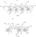
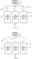
- FIG. 1 is a schematic diagram of an antenna assembly provided in an implementation of the present disclosure.
- the antenna assembly 10 includes a first antenna 110 and a second antenna 120.
- the first antenna 110 includes a first radiator 111, a first signal-source 112, a first matching circuit 113, and a first adjusting circuit 114.
- the first signal-source 112 is electrically connected to the first radiator 111 through the first matching circuit 113.
- the first adjusting circuit 114 is electrically connected to the first matching circuit 113 or the first radiator 111, and is configured to adjust a resonant frequency-point of the first antenna 110, so that transmission/reception of an electromagnetic wave signal in a first frequency band is supported by the first antenna 110.
- the second antenna 120 includes a second radiator 121, a second signal-source 122, a second matching circuit 123, and a second adjusting circuit 124.
- the second signal-source 122 is electrically connected to the second radiator 121 through the second matching circuit 123.
- the second adjusting circuit 124 is electrically connected to the second matching circuit 123 or the second radiator 121.
- the second adjusting circuit 124 is configured to adjust a resonant frequency-point of the second antenna 120, so that transmission/reception of an electromagnetic wave signal in a second frequency band and a third frequency band is supported by the second antenna 120.
- the electromagnetic wave signal in the second frequency band and the third frequency band include a frequency band covered by a first resonant mode corresponding to a higher-order mode of the second antenna 120.
- the first adjusting circuit 114 is electrically connected to the first matching circuit 113 or the first radiator 111
- the second adjusting circuit 124 is electrically connected to the second matching circuit 123 or the second radiator 121
- these cases may be randomly combined as follows.
- the second adjusting circuit 124 is electrically connected to the first matching circuit 113 and the second adjusting circuit 124 is electrically connected to the second matching circuit 123; or, the second adjusting circuit 124 is electrically connected to the first matching circuit 113 and the second adjusting circuit 124 is electrically connected to the second radiator 121; or, the second adjusting circuit 124 is electrically connected to the first matching circuit 113 and the second adjusting circuit 124 is electrically connected to the second radiator 121; or, the first adjusting circuit 114 is electrically connected to the first radiator 111 and the second adjusting circuit 124 is electrically connected to the second radiator 121.
- the first adjusting circuit 114 is electrically connected to the first matching circuit 113 and the second adjusting circuit 124 is electrically connected to the second radiator
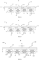
- FIG. 2 to FIG. 4 are schematic diagrams of antenna assemblies provided in other implementations of the present disclosure.
- the first adjusting circuit 114 is electrically connected to the first matching circuit 113, and the second adjusting circuit 124 is electrically connected to the second radiator 121.
- the first adjusting circuit 114 is electrically connected to the first radiator 111, and the second adjusting circuit 124 is electrically connected to the second matching circuit 123.
- the first adjusting circuit 114 is electrically connected to the first radiator 111, and the second adjusting circuit 124 is electrically connected to the second radiator 121.
- the antenna assembly 10 including the first antenna 110 and the second antenna 120 does not exclude that the antenna assembly 10 includes other antennas in addition to the first antenna 110 and the second antenna 120.
- a signal source refers to a component that generates an excitation signal.
- the first antenna 110 is configured to receive an electromagnetic wave signal
- the first signal-source 112 generates a first excitation signal
- the first excitation signal is loaded onto the first radiator 111 (in this implementation, a first feed point 1113) through the first matching circuit 113, so that the first radiator 111 radiates an electromagnetic wave signal.
- the second antenna 120 is configured to receive an electromagnetic wave signal
- the second signal-source 122 generates a second excitation signal
- the second excitation signal is loaded onto the second radiator 121 (in this implementation, a second feed point 1213) through the second matching circuit 123, so that the second radiator 121 receives and transmits an electromagnetic wave signal.
- the first radiator 111 may be a flexible printed circuit (FPC) antenna radiator, a laser direct structuring (LDS) antenna radiator, or a printed direct structuring (PDS) antenna radiator, or a metal bracket.
- the second radiator 121 may be an FPC antenna radiator, an LDS antenna radiator, a PDS antenna radiator, or a metal branch. It can be understood that types of the first radiator 111 and the second radiator 121 may be the same or different.
- the first resonant mode corresponding to the higher-order mode of the second antenna 120 will be described later with reference to a simulation diagram.
- the first resonant mode corresponding to the higher-order mode of the second antenna 120 covers part of in the second frequency band and the third frequency band, so that transmission/reception of an electromagnetic wave signal in the first frequency band, the second frequency band, and the third frequency band is supported by the antenna assembly 10.
- the antenna assembly 10 has a wide bandwidth and better communication performance
- the first frequency band includes a lower band (LB)
- the second frequency band includes a middle high band (MHB)
- the third frequency band includes an ultra-high band (UHB).
- the LB refers to a frequency band with a frequency lower than 1000 MHz, the MHB ranges from 1000 MHz to 3000 MHz, and the UHB ranges from 3000 MHz to 6000 MHz.
- the antenna assembly 10 further has a second resonant mode, a third resonant mode, and a fourth resonant mode.
- the antenna assembly 10 is operable in the first resonant mode, the second resonant mode, the third resonant mode, and the fourth resonant mode together to support transmission/reception of the electromagnetic wave signal in the second frequency band and the third frequency band.
- the second radiator 121 is spaced apart from and coupled with and the first radiator 111.
- the second radiator 121 is spaced apart from and coupled with the first radiator 111, that is, the first radiator 111 and the second radiator 121 are shared-aperture. Due to the coupling effect between the first radiator 111 and the second radiator 121, when the first antenna 110 operates, not only the first radiator 111 is configured to receive and transmit an electromagnetic wave signal, but also the second radiator 121 is configured to receive and transmit an electromagnetic wave signal, so that the first antenna 110 can operate in a relatively wide frequency-band.
- radiators in the antenna assembly 10 are multiplexed, and space is multiplexed, thereby facilitating the reduction of the size of the antenna assembly 10. It can be seen from the above analysis that the antenna assembly 10 has a small size, and when the antenna assembly 10 is applied to the electronic device 1, the antenna assembly 10 is easily stacked with other devices in the electronic device 1.
- FIG. 5 is an equivalent schematic diagram of the antenna assembly including the first adjusting circuit as illustrated in FIG. 3 implementing low-impedance to ground in the second frequency band and the third frequency band.
- the first adjusting circuit 114 implements low-impedance to ground of an electromagnetic wave signal in the second frequency band and in the third frequency band, and part of the first radiator 111 from a connection point where the first adjusting circuit 114 is connected to the first radiator 111 to a ground end (a first ground end 1111) of the first radiator 111 is equivalent to zero.
- An equivalent antenna assembly 10 is as illustrated in FIG. 5 , which will be described later in combination with the simulation diagram of S-parameters.
- the first radiator 111 has a first ground end 1111, a first free end 1112, a first feed point 1113, and a first connection point 1114.
- the first ground end 1111 is grounded, the first free end 1112 is spaced apart from and coupled with the second radiator 121, the first feed point 1113 is spaced apart from the first connection point 1114, and the first feed point 1113 and the first connection point 1114 are located between the first ground end 1111 and the first free end 1112.
- the first connection point 1114 is located between the first feed point 1113 and the first free end 1112.
- the first connection point 1114 may also be located between the first feed point 1113 and the first ground end 1111.
- the second radiator 121 further includes a second ground end 1211 and a second free end 1212, the second ground end 1211 is grounded, the second free end 1212 is spaced apart from the first free end 1112, and the second feed point 1213 is located between the second ground end 1211 and the second free end 1212.
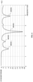
- FIG. 6 is a simulation diagram of part of S-parameters of the antenna assembly as illustrated in FIG. 3 .
- the abscissa represents frequency in unit of GHz
- the ordinate represents S-parameters in unit of dB.
- the antenna assembly 10 has a first resonant mode (marked as mode 1 in the figure), a second resonant mode (marked as mode 2 in the figure), a third resonant mode (marked as mode 3 in the figure), and a fourth resonant mode (marked as mode 4 in the figure).
- the first resonant mode is a 1/8 wavelength mode of the second antenna 120
- the second resonant mode is a 1/4 wavelength mode from the first adjustment circuit 114 to a gap between the first radiator 111 and the second radiator 121
- the third resonant mode is a 1/4 wavelength mode of the second antenna 120
- the fourth resonant mode is a 1/4 wavelength mode from the second signal-source 122 to the gap between the second radiator 121 and the first radiator 111.
- a sequence of appearance of each resonant mode changes according to a change of the length of the first radiator 111 and a change of the length of the second radiator 121.
- the second resonant mode, the third resonant mode, and the fourth resonant mode herein are 1/4 wavelength modes, that is, basic modes.
- the second resonant mode is a fundamental mode
- the first resonant mode has a higher transmit/receive power
- the third resonant mode is a fundamental mode
- the third resonant mode has a higher transmit/receive power
- the fourth resonant mode is a fundamental mode
- the fourth resonant mode has high transmit/receive power.
- the second resonant mode, the third resonant mode, and the fourth resonant mode may also be higher-order modes, and although the transmit/receive power of a higher-order mode is smaller than the transmit/receive power of the fundamental mode, as long as the first resonant mode, the second resonant mode, the third resonant mode, and the fourth resonant mode together implement transmission/reception of the electromagnetic wave signal in the second frequency band and the third frequency band.
- the first resonant mode, the second resonant mode, the third resonant mode, and the fourth resonant mode may cover transmission/reception of an electromagnetic wave signal in MHB and UHB. That is, transmission/reception of an electromagnetic wave signal in a frequency-band range of 1000 MHz ⁇ 6000 MHz are achieved.
- FIG. 7 is a schematic diagram of a first adjusting circuit provided in an implementation of the present disclosure.
- the first adjusting circuit 114 includes multiple adjusting sub-circuits and a switch unit. Under control of a control signal, the switch unit is configured to electrically connect at least one adjusting sub-circuit in the multiple adjusting sub-circuits to the first matching circuit 113 or the first radiator 111.
- the adjusting sub-circuits included in the first adjusting circuit 114 are named as first adjusting sub-circuits 1141, and the switch unit in the first adjusting circuit 114 is named as the first switch unit 1142.
- the first switch unit 1142 is electrically connected to the first connection point 1114, the first switch unit 1142 is further electrically connected to the multiple first sub-adjustment circuits 1141 to be grounded, and under the control of the control signal, the first switch unit 1142 is configured to electrically connect at least one first sub-adjustment circuit 1141 in the multiple first sub-adjustment circuits 1141 to the first connection point 1114.
- the first adjusting sub-circuit 1141 includes two first adjusting sub-circuits 1141, and accordingly, the first switch unit 1142 is a single-pole double-throw (SPDT) switch.
- a movable terminal of the first switch unit 1142 is electrically connected to the first connection point 1114, one fixed terminal of the first switch unit 1142 is electrically connected to one of the first adjusting sub-circuits 1141 to be grounded, and the other fixed terminal of the first switch unit 1142 is electrically connected to the other one of the first adjusting sub-circuits 1141 to be grounded.
- the first adjusting circuit 114 includes N first adjusting sub-circuits 1141. Accordingly, the first switch unit 1142 is a single-pole N-throw (SPNT) switch, or the first switch unit 1142 is an N-pole N-throw (NPNT) switch, where N ⁇ 2, and N is a positive integer.
- SPNT single-pole N-throw
- NPNT N-pole N-throw
- FIG. 8 is a schematic diagram of a first adjusting circuit provided another implementation of the present disclosure.
- the first adjusting circuit 114 includes M first adjusting sub-circuits 1141 and M first switch units 1142, and each of the first switch units 1142 is connected in series with one of the first adjusting sub-circuits 1141, where M ⁇ 2, and N is a positive integer.
- first adjusting sub-circuit 1141 and the first switch unit 1142 in the first adjusting circuit 114 are not limited to those described above, as long as the first switch unit 1142 is capable of electrically connect at least one first adjusting sub-circuit 1141 in the multiple first adjusting sub-circuits 1141 to the first connection point 1114 under the control of the control signal.
- the first adjusting sub-circuit 1141 includes at least one or any combination of a capacitor, an inductor, or a resistor. Therefore, the first adjusting sub-circuit 1141 is also referred to as a lumped circuit.
- FIG. 9 is a simulation diagram of a first adjusting circuit switching among frequency bands supported by the first antenna in the first frequency band.
- the abscissa represents frequency in units of GHz
- the ordinate represents S-parameters in units of dB.
- curve 1 is band 5 (B5)
- curve 2 is Band 8 (B8)
- curve 3 is Band 28 (B28).
- the first adjusting circuit 114 is further configured to switch among frequency bands supported by the first antenna 110 in the first frequency band.
- the frequency bands supported in the first frequency band include, but are not limited to, B28, B5, and B8.
- the first adjusting circuit 114 is configured to enable the first antenna 110 to work in any one of B28, band 20 (B20), B5, or B8 and to be switchable among B28, B5 and B8.
- frequency bands supported in the first frequency band include, but are not limited to, B28, B20, B5, and B8.
- the first adjusting circuit 114 includes four first adjusting sub-circuits. Specifically, the first adjusting circuit 114 includes a first inductor 114a, a second inductor 114b, a third inductor 114c, and a capacitor 114d. The first inductor 114a, the second inductor 114b, and the third inductor 114c have different inductance.
- the first switch unit 1142 includes a common terminal P, a first switch sub-unit 1143, a second switch sub-unit 1144, a third switch sub-unit 1145, and a fourth switch sub-unit 1146.
- the common terminal P is electrically connected to the first matching circuit 113, one end of the first switch sub-unit 1143 is electrically connected to the first inductor 114a, and the other end of the first switch sub-unit 1143 is electrically connected to the common terminal P.
- One end of the second switch sub-unit 1144 is electrically connected to the second inductor 114b, and the other end of the second switch sub-unit 1144 is electrically connected to the common terminal P.
- One end of the third switch sub-unit 1145 is electrically connected to the third inductor 114c, and the other end of the third switch sub-unit 1145 is electrically connected to the common terminal P.
- One end of the fourth switch sub-unit 1146 is electrically connected to the capacitor 114d, and the other end of the fourth switch sub-unit 1146 is electrically connected to the common terminal P.
- the first matching circuit 113 includes a first matching inductor L11, a first matching capacitor C11, a second matching inductor L12, a second matching capacitor C12, a third matching capacitor C13, and a third matching inductor L13.
- One end of the first matching inductor L11 is electrically connected to the first signal-source 112
- the other end of the first matching inductor L11 is electrically connected to the first radiator 111 through the first matching capacitor C11 and the second matching inductor L12 in sequence, and a connection point between the first matching capacitor C11 and the second matching inductor L12 is electrically connected to the common terminal P.
- One end of the second matching capacitor C12 is electrically connected to a connection point between the first matching inductor L11 and the first matching capacitor C11, and the other end of the second matching capacitor C12 is grounded.
- One end of the third matching capacitor C13 is electrically connected to the first radiator 111, and the other end the third matching capacitor C13 is grounded.
- One end of the third matching inductor L 13 is electrically connected to the first radiator 111, and the other end of the third matching inductor L13 is grounded.
- the third matching capacitor C13 includes a first matching sub-capacitor C01 and a second matching sub-capacitor C02, one end of the first matching sub-capacitor C01 is electrically connected to the first radiator 111, and the other end of the first matching sub-capacitor C01 is electrically connected to second matching sub-capacitor C02 to be grounded.
- a matching capacitor is also a capacitor, and a matching inductor is also an inductor.
- the third matching capacitor C13 includes two capacitors (the first matching sub-capacitor C01 and the second matching sub-capacitor C02) connected in series.
- the third matching capacitor C13 includes two capacitors connected in series, which can facilitate selecting an appropriate capacitor to achieve a capacitance.
- the first matching circuit 113 includes one or more frequency-selective filter sub-circuits 113a
- the second matching circuit 123 includes one or more frequency-selective filter sub-circuits 113a.
- the frequency-selective filter sub-circuits 113a are further configured to isolate the first antenna 110 from the second antenna 120.
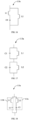
- FIGS. 11 to 18 together where FIGS. 11 to 18 are schematic diagrams of frequency-selective filter sub-circuits provided in various implementations, respectively.
- the frequency-selective filter sub-circuit 113a includes one or more of the following circuits.
- the frequency-selective filter sub-circuit 113a includes a band-pass circuit formed by an inductor L0 and a capacitor C0 connected in series.
- the frequency-selective filter sub-circuit 113a includes a band-stop circuit formed by an inductor L0 and a capacitor C0 connected in parallel.
- the frequency-selective filter sub-circuit 113a includes an inductor L0, a first capacitor C1, and a second capacitor C2.
- the inductor L0 is connected in parallel with the first capacitor C1, and the second capacitor C2 is electrically connected to a node where the inductor L0 is electrically connected to the first capacitor C1.
- the frequency-selective filter sub-circuit 113a includes a capacitor C0, a first inductor L1, and a second inductor L2.
- the capacitor C0 is connected in parallel with the first inductor L1, and the second inductor L2 is electrically connected to a node where the capacitor C0 is electrically connected to the first inductor L1.
- the frequency-selective filter sub-circuit 113a includes an inductor L0, a first capacitor C1, and a second capacitor C2.
- the inductor L0 is connected in series with the first capacitor C1, one end of the second capacitor C2 is electrically connected to a first end of the inductor L0 that is not connected to the first capacitor C1, and the other end of the second capacitor C2 is electrically connected to one end of the first capacitor C1 that is not connected to the inductor L0.
- the frequency-selective filter sub-circuit 113a includes a capacitor C0, a first inductor L1, and a second inductor L2.
- the capacitor C0 is connected in series with the first inductor L1, one end of the second inductor L2 is electrically connected to one end of the capacitor C0 that is not connected to the first inductor L1, and the other end of the second inductor L2 is electrically connected to one end of the first inductor L1 that is not connected to the capacitor C0.
- the frequency-selective filter circuit 113a includes a first capacitor C1, a second capacitor C2, a first inductor L1, and a second inductor L2.
- the first capacitor C1 is connected in parallel with the first inductor L1
- the second capacitor C2 is connected in parallel with the second inductor L2, and one end of an entirety formed by the second capacitor C2 and the second inductor L2 connected in parallel is electrically connected to one end of an entirety formed by the first capacitor C1 and the first inductor L1 connected in parallel.
- the frequency-selective filter sub-circuit 113a includes a first capacitor C1, a second capacitor C2, a first inductor L1, and a second inductor L2.
- the first capacitor C1 is connected in series with the first inductor L1 to form a first unit 113b
- the second capacitor C2 is connected in series with the second inductor L2 to form a second unit 113c
- the first unit 113b is connected in parallel with the second unit 113c.
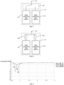
- FIG. 19 is a schematic diagram of a second adjusting circuit provided in an implementation of the present disclosure.
- the second adjusting circuit 124 includes multiple adjusting sub-circuits and multiple switch units.
- each adjusting sub-circuit included in the second adjusting circuit 124 is named as a second adjusting sub-circuit 1241
- each switch unit included in the second adjusting circuit 124 is named as a second switch unit 1242.
- the second switch units 1242 are configured to electrically connect at least one of the multiple second adjusting sub-circuits 1241 in the second adjusting circuit 124 to the second matching circuit 123 or the second radiator 121, under control of a control signal.
- the second matching circuit 123 is connected.
- the second adjusting circuit 124 includes three switch units and three second adjusting sub-circuits 1241. Each switch unit 1242 is electrically connected to a second adjusting sub-circuit 1241.
- the second adjusting circuit 124 includes a single-pole three-throw (SP3T) switch and three second adjusting sub-circuits 1241.
- SP3T single-pole three-throw
- a movable terminal of the SP3T switch is electrically connected to the second matching circuit 123, and three fixed terminals of the SP3T switch are electrically connected to the three second adjusting sub-circuits 1241, respectively.
- the second adjusting circuit 124 includes K second adjusting sub-circuits 1241.
- the second switch unit 1242 is a single-pole K-throw (SPKT) switch, or the second switch unit 1242 is a K-pole K-throw (KPKT) switch, where K is a positive integer greater than or equal to 2.
- the second adjusting sub-circuit 1241 includes at least one of a capacitor, an inductor, or a resistor, or any combination thereof. Therefore, the second adjusting sub-circuit 1241 is also referred to as a lumped circuit. It can be understood that the second adjusting sub-circuit 1241 of the first adjusting circuit 114 and the second adjusting sub-circuit 1241 of the second adjusting circuit 124 may be the same or different.
- the first adjusting circuit 114 and the second adjusting circuit 124 modulate together, so that the antenna assembly 10 can implement transmission/reception of an electromagnetic wave signal in the first frequency band, the second frequency band, and the third frequency band, thereby implementing carrier aggregation (CA) and EADC in LB+ MHB+UHB.
- CA carrier aggregation
- EADC EADC in LB+ MHB+UHB.
- the abscissa represents frequency in units of GHz
- the ordinate represents S-parameters in units of dB.
- curve 5 represents S1,1 parameter
- curve 6 represents S2,2 parameter
- curve 7 represents S2,1 parameter. It can be seen from the simulation diagram that a resonant frequency-band corresponding to curve 5 is LB, and a resonant frequency-band corresponding to curve 6 is MHB and UHB. It can be seen from curve 7 that LB has a higher isolation from MHB and UHB, respectively.
- the first antenna 110 and the second antenna 120 are together configured to realize long term evolution (LTE) new radio (NR) double connect (ENDC) and CA in a LB+MHB+UHB (a frequency-band range of 0 MHz -6000 MHz).
- LTE long term evolution
- NR new radio
- ECC double connect
- CA CA in a LB+MHB+UHB (a frequency-band range of 0 MHz -6000 MHz).
- the first antenna 110 and the second antenna 120 in the antenna assembly 10 are configured to implement ENDC in a range of 0MHz ⁇ 6000MHz. It can be seen that the antenna assembly 10 of the present disclosure can realize ENDC and can support both a fourth generation mobile communications technology (4G) wireless access network and fifth generation mobile communications technology (5G)-NR. Therefore, the antenna assembly 10 provided in implementations of the present disclosure can improve a transmission bandwidth of 4G and 5G, improve uplink and downlink rates, and have a better communication effect.
- 4G fourth generation mobile communications technology
- 5G-NR fifth generation mobile communications technology
- the first antenna 110 and the second antenna 120 are cooperatively configured to implement ENDC and CA in LB+MHB+UHB (a frequency-band range of 0MHz ⁇ 6000MHz). Therefore, the first antenna 110 and the second antenna 120 may be cooperatively configured to implement ENDC and CA in a frequency-band range of 1000MHz ⁇ 6000MHz. In other words, the first antenna 110 and the second antenna 120 together implement ENDC and CA in MHB+UHB.
- the first radiator 111 has a first ground end 1111, a first free end 1112, a first feed point 1113, and a first connection point 1114.
- the first ground end 1111 is grounded, and the first free end 1112 is spaced apart from and coupled with the second radiator 121.
- the first feed point 1113 and the first connection point 1114 are located between the first ground end 1111 and the first free end 1112.
- the first signal-source 112 is electrically connected to the first feed point 1113 of the first radiator 111 through the first matching circuit 113.
- the first adjusting circuit 114 When the first adjusting circuit 114 is electrically connected to the first radiator 111, the first adjusting circuit 114 is electrically connected to the first connection point 1114 of the first radiator 111, where the first connection point 1114 is located between the first ground end 1111 and the first feed point 1113, or the first connection point 1114 is located between the first feed point 1113 and the first free end 1112.
- the second radiator 121 has a second ground end 1211, a second free end 1212, a second feed point 1213, and a second connection point 1214.
- the second ground end 1211 is grounded, and the second free end 1212 is spaced apart from and coupled with the first radiator 111.
- the first free end 1112 of the first radiator 111 is spaced apart from and coupled with the second free end 1212 of the second radiator 121.
- the second feed point 1213 and the second connection point 1214 are located between the second ground end 1211 and the second free end 1212.
- the second signal-source 122 is electrically connected to the second feed point 1213 of the second radiator 121 through the second matching circuit 123.
- the second adjusting circuit 124 When the second adjusting circuit 124 is electrically connected to the second radiator 121, the second adjusting circuit 124 is electrically connected to the second connection point 1214 of the second radiator 121, where the second connection point 1214 is located between the second ground end 1211 and the second feed point 1213, or the second connection point 1214 is located between the second feed point 1213 and the second free end 1212.
- the first connection point 1114 is located between the first ground end 1111 and the first feed point 1113, or the first connection point 1114 is located between the first feed point 1113 and the first free end 1112.
- the second adjusting circuit 124 is electrically connected to the second connection point 1214 of the second radiator 121, where the second connection point 1214 is located between the second ground end 1211 and the second feed point 1213, or the second connection point 1214 is located between the second feed point 1213 and the second free end 1212. Therefore, positions of the first connection point 1114 and the second connection point 1214 in the antenna assembly 10 may include any combination of the following.
- the first connection point 1114 is located between the first ground end 1111 and the first feed point 1113, and the second connection point 1214 is located between the second ground end 1211 and the second feed point 1213 (see FIG. 23 ); or the first connection point 1114 is located between the first ground end 1111 and the first feed point 1113, and the second connection point 1214 is located between the second feed point 1213 and the second free end 1212 (see FIG. 24 ); or the first connection point 1114 is located between the first feed point 1113 and the first free end 1112, and the second connection point 1214 is located between the second ground end 1211 and the second feed point 1213 (see FIG. 25 ); or, the first connection point 1114 is located between the first feed point 1113 and the first free end 1112, and the second connection point 1214 is located between the second feed point 1213 and the second free end 1212 (see FIG. 4 ).
- the first connection point 1114 When the first connection point 1114 is located between the first feed point 1113 and the first free end 1112, an influence of an electromagnetic wave signal (an electromagnetic wave signal in the first frequency band and an electromagnetic wave signal supported by the first resonant mode) generated by the first radiator 111 on electromagnetic wave signals in other frequency bands supported by the antenna assembly 10 for receiving and transmitting can be reduced. It can be understood that, the first connection point 1114 may also be located between the first feed point 1113 and the first ground end 1111, as long as the first adjusting circuit 114 can be electrically connected to the first radiator 111.
- the second connection point 1214 When the second connection point 1214 is located between the second feed point 1213 and the second free end 1212, an influence of an electromagnetic wave signal generated by the second radiator 121 on electromagnetic wave signals in other frequency bands supported by the antenna assembly 10 for receiving and transmitting can be reduced. It can be understood that, the second connection point 1214 may also be located between the second feed point 1213 and the second ground end 1211, as long as the second adjusting circuit 124 can be electrically connected to the second radiator 121.
- FIG. 26 is a schematic diagram illustrating a dimension of a gap between the first radiator and the second radiator in the antenna assembly provided in an implementation of the present disclosure.
- the dimension d of the gap between the first radiator 111 and the second radiator 121 satisfies: 0.5mm ⁇ d ⁇ 1.5mm.
- the gap between the first antenna 110 radiator and the second antenna 120 radiator in the antenna assembly 10 always meet: 0.5 mm ⁇ d ⁇ 1.5 mm.
- a better coupling effect between the first radiator 111 and the second radiator 121 may be ensured.
- the sizes of the first radiator 111 and the second radiator 121 in the antenna assembly 10 are illustrated in the antenna assembly 10 as illustrated in FIG. 1 , however, it should not be understood as a limitation to the present disclosure, and the gap between the first radiator 111 and the second radiator 121 is also applicable to the antenna assembly 10 provided in other implementations.
- FIG. 27 is a three-dimensional structural diagram of an electronic device provided in an implementation of the present disclosure.
- the electronic device 1 includes the antenna assembly 10 according to any foregoing implementation.
- the electronic device 1 further includes a middle frame 30, a screen 40, a circuit board 50, and a battery cover 60.
- the middle frame 30 is made of metal, such as aluminum magnesium alloy.
- the middle frame 30 generally serves as the ground of the electronic device 1.
- a ground system in the electronic device 1 not only includes the middle frame 30, but also includes a ground on the circuit board 50 and a ground in the screen 40.
- the screen 40 may be a display screen with a display function, and may also be a screen 40 integrated with a display function and a touch control function.
- the screen 40 is configured to display information such as a text, an image, and a video.
- the screen 40 is carried on the middle frame 30 and disposed on one side of the middle frame 30.
- the circuit board 50 is also generally carried on the middle frame 30, and the circuit board 50 and the screen 40 are carried on two opposite sides of the middle frame 30. At least one or more of the first signal-source 112, the second signal-source 122, the first matching circuit 113, the second matching circuit 123, the first adjusting circuit 114, and the second adjusting circuit 124 in the antenna assembly 10 described above may be disposed on the circuit board 50.
- the battery cover 60 is disposed on one side of the circuit board 50 away from the middle frame 30.
- the battery cover 60, the middle frame 30, the circuit board 50, and the screen 40 cooperate with each other to form a complete electronic device 1. It should be understood that, the structural description of the electronic device 1 is only a description of one form of the structure of the electronic device 1, should not be understood as a limitation to the electronic device 1, and should not be understood as a limitation to the antenna assembly 10.
- the first radiator 111 When the first radiator 111 is electrically connected to the ground of the middle frame 30, the first radiator 111 may be connected to the ground of the middle frame 30 through a connecting bar, or the first radiator 111 may also be electrically connected to the ground of the middle frame 30 through a conductive elastic sheet.
- the second radiator 121 when the second radiator 121 is electrically connected to the ground of the middle frame 30, the second radiator 121 may also be connected to the ground of the middle frame 30 through a connecting rib, or the second radiator 121 may also be electrically connected to the ground of the middle frame 30 through a conductive elastic sheet.
- the middle frame 30 includes a frame body 310 and an edge frame 320.
- the edge frame 320 is bendably connected to a periphery of the frame body 310. Any of the first radiator 111, the second radiator 121, the third radiator 131, or the fourth radiator 141 in the foregoing implementations may be formed on the edge frame 320.
- the first radiator 111 and the second radiator 121 may also be formed on the edge frame 320, or the first radiator 111 and the second radiator 121 each may be a FPC antenna radiator, a LDS antenna radiator, a PDS antenna radiator, or a metal branch.
- FIG. 29 is a schematic diagram illustrating positions in an electronic device provided in an implementation.
- the electronic device 1 includes a top portion 1a and a bottom portion 1b, and the first radiator 111 and the second radiator 121 are both disposed on the top portion 1a.
- the top portion 1a refers to an upper part of the electronic device 1 when the electronic device 1 is in use, and the bottom portion 1b is opposite to the top portion 1a and refers to a lower part of the electronic device 1.
- the electronic device 1 in this implementation includes a first side 11, a second side 12, a third side 13, and a fourth side 14 that are sequentially connected to one another end to end.
- the first side 11 and the third side 13 are short sides of the electronic device 1, and the second side 12 and the fourth side 14 are long sides of the electronic device 1.
- the first side 11 and the third side 13 are opposite to each other and spaced apart from each other, the second side 12 and the fourth side 14 are opposite to each other and spaced apart from each other.
- the second side 12 is connected to the first side 11 and the third side 13 in a bending manner, and the fourth side 14 is connected to the first side 11 and the third side 13 in a bending manner.
- a connection between the first side 11 and the second side 12, a connection between the second side 12 and the third side 13, a connection between the third side 13 and the fourth side 14, and a connection between the fourth side 14 and the first side 11 all form corners of the electronic device 1.
- the first side 11 is a top side
- the second side 12 is a right side
- the third side 13 is a lower side
- the fourth side 14 is a left side.
- the first side 11 and the second side 12 define an upper right corner
- the first side 11 and the fourth side 14 define an upper left corner.
- the top portion 1a includes three cases: the first radiator 111 and the second radiator 121 are disposed at the upper left corner of the electronic device 1; or, the first radiator 111 and the second radiator 121 are disposed at the top side of the electronic device 1; or the first radiator 111 and the second radiator 121 are disposed at the upper right corner of the electronic device 1.
- the first radiator 111 and the second radiator 121 being disposed at the upper left corner of the electronic device 1 includes following cases: part of the first radiator 111 is disposed at the left side, the other part of the first radiator 111 is disposed at the top side, and the second radiator 121 is disposed at the top side; or, part of the second radiator 121 is disposed at the top side, the other part of the second radiator 121 is disposed at the left side, and the first radiator 111 is disposed at the left side.
- the first radiator 111 and the second radiator 121 being disposed at the upper right corner of the electronic device 1 includes following cases: part of the first radiator 111 is disposed at the top side, the other part of the first radiator 111 is disposed at the right side, and the second radiator 121 is disposed at the right side; or, part of the second radiator 121 is disposed at the right side, the other part of the second radiator 121 is disposed at the top side, and part of the first radiator 111 is disposed at the top side
- the top portion 1a of the electronic device 1 When the electronic device 1 is placed upright, the top portion 1a of the electronic device 1 is usually away from the ground, and the bottom portion 1b of the electronic device 1 is usually close to the ground.
- the first radiator 111 and the second radiator 121 are disposed on the top portion 1a, upper hemisphere radiation efficiency of the first antenna 110 and the second antenna 120 is better, so that the first antenna 110 and the second antenna 120 have better communication efficiency.
- the first radiator 111 and the second radiator 121 may also be disposed on the bottom portion 1b of the electronic device 1,
- the first antenna 110 and the second antenna 120 do not have good upper hemisphere radiation efficiency, but the first antenna 110 and the second antenna 120 may also have good communication effect as long as the upper hemisphere radiation efficiency is greater than or equal to the preset efficiency.
Landscapes
- Engineering & Computer Science (AREA)
- Computer Networks & Wireless Communication (AREA)
- Details Of Aerials (AREA)
Abstract
Description
- This disclosure relates to the field of communication technology, and in particular, to an antenna assembly and an electronic device.
- With the development of technologies, electronic devices with communication functions, such as mobile phones, are becoming increasingly popular and increasingly powerful. The electronic device generally includes an antenna assembly to implement a communication function of the electronic device. However, in the related art, communication performance of the antenna assembly in the electronic device is not good enough, and needs to be improved.
- According to a first aspect, an antenna assembly is provided in implementations of the present disclosure. The antenna assembly includes a first antenna and a second antenna.
- The first antenna includes a first radiator, a first signal-source, a first matching circuit, and a first adjusting circuit. The first signal-source is electrically connected to the first radiator through the first matching circuit, and the first adjusting circuit is electrically connected to the first matching circuit or the first radiator, and configured to adjust a resonant frequency-point of the first antenna to make the first antenna support transmission/reception of an electromagnetic wave signal in a first frequency band.
- The second antenna includes a second radiator, a second signal-source, a second matching circuit, and a second adjusting circuit. The second signal-source is electrically connected to the second radiator through the second matching circuit, and the second adjusting circuit is electrically connected to the second matching circuit or the second radiator, and configured to adjust a resonant frequency-point of the second antenna to make the second antenna support transmission/reception of an electromagnetic wave signal in a second frequency band and a third frequency band, where the electromagnetic wave signal in the second frequency band and the third frequency band includes a frequency band covered by a first resonant mode corresponding to a higher-order mode of the second antenna.
- According to a second aspect, an electronic device is provided in implementations of the present disclosure. The electronic device includes the antenna assembly according to the first aspect.
- To describe technical solutions in implementations of the present disclosure more clearly, the following will give a brief introduction to accompanying drawings required for describing implementations or the related art. Apparently, the accompanying drawings described hereinafter are merely some implementations of the disclosure. Based on these drawings, those of ordinary skill in the art can also obtain other drawings without creative effort.
-
FIG. 1 is a schematic diagram of an antenna assembly provided in an implementation of the present disclosure. -
FIG. 2 to FIG. 4 are schematic diagrams of antenna assemblies provided in other implementations of the present disclosure. -
FIG. 5 is an equivalent schematic diagram of the antenna assembly including the first adjusting circuit as illustrated inFIG. 3 implementing low-impedance to ground in a second frequency band and a third frequency band. -
FIG. 6 is simulation diagram of part of S-parameters of the antenna assembly as illustrated inFIG. 3 . -
FIG. 7 is a schematic diagram of a first adjusting circuit provided in an implementation of the present disclosure. -
FIG. 8 is a schematic diagram of a first adjusting circuit provided in another implementation of the present disclosure. -
FIG. 9 is a simulation diagram of a first adjusting circuit switching among frequency bands supported by a first antenna in a first frequency band. -
FIG. 10 is an equivalent circuit diagram of a first antenna in the antenna assembly inFIG. 1 . -
FIGS. 11 to 18 are schematic diagrams of frequency-selective filter sub-circuits provided in various implementations. -
FIG. 19 is a schematic diagram of a second adjusting circuit provided in an implementation of the present disclosure. -
FIG. 20 is a schematic diagram of a second adjusting circuit provided in an implementation of the present disclosure. -
FIG. 21 is a simulation diagram of S-parameters of the antenna assembly as illustrated inFIG. 1 . -
FIG. 22 is a simulation diagram of isolation of the antenna assembly as illustrated inFIG. 1 . -
FIG. 23 is a schematic diagram of an antenna assembly provided in another implementation of the present disclosure. -
FIG. 24 is a schematic diagram of an antenna assembly provided in another implementation of the present disclosure. -
FIG. 25 is a schematic diagram of an antenna assembly provided in another implementation of the present disclosure. -
FIG. 26 is a schematic diagram illustrating a dimension of a gap between a first radiator and a second radiator in an antenna assembly provided in an implementation of the present disclosure. -
FIG. 27 is a three-dimensional structural diagram of an electronic device provided in an implementation of the present disclosure. -
FIG. 28 is a cross-sectional view taken along line I-I inFIG. 27 provided in an implementation. -
FIG. 29 is a schematic diagram illustrating positions in an electronic device provided in an implementation. - In a first aspect, an antenna assembly is provided in the present disclosure. The antenna assembly includes a first antenna and a second antenna.
- The first antenna includes a first radiator, a first signal-source, a first matching circuit, and a first adjusting circuit, where the first signal-source is electrically connected to the first radiator through the first matching circuit, and the first adjusting circuit is electrically connected to the first matching circuit or the first radiator, and configured to adjust a resonant frequency-point of the first antenna to make the first antenna support transmission/reception of an electromagnetic wave signal in a first frequency band. The second antenna includes a second radiator, a second signal-source, a second matching circuit, and a second adjusting circuit, where the second signal-source is electrically connected to the second radiator through the second matching circuit, and the second adjusting circuit is electrically connected to the second matching circuit or the second radiator, and configured to adjust a resonant frequency-point of the second antenna to make the second antenna support transmission/reception of an electromagnetic wave signal in a second frequency band and a third frequency band. The electromagnetic wave signal in the second frequency band and the third frequency band includes a frequency band covered by a first resonant mode corresponding to a higher-order mode of the second antenna.
- In an implementation, the antenna assembly further has a second resonant mode, a third resonant mode, and a fourth resonant mode, where transmission/reception of the electromagnetic wave signal in the second frequency band and the third frequency band is supported by the first resonant mode, the second resonant mode, the third resonant mode, and the fourth resonant mode.
- In an implementation, the first resonant mode is a 1/8 wavelength mode of the second antenna, and the second resonant mode is a 1/4 wavelength mode from the first adjusting circuit to a gap between the first radiator and the second radiator; and the third resonant mode is a 1/4 wavelength mode of the second antenna, and the fourth resonant mode is a 1/4 wavelength mode from the second signal-source to the gap between the second radiator and the first radiator.
- In an implementation, the first frequency band includes a lower band (LB), the second frequency band includes a middle high band (MHB), and the third frequency band includes an ultra-high band (UHB).
- In an implementation, the first adjusting circuit is further configured to switch among frequency bands supported by the first antenna in the first frequency band.
- In an implementation, the first adjusting circuit includes multiple adjusting sub-circuits and a switch unit, and the switch unit is configured to electrically connect, under control of a control signal, at least one adjusting sub-circuit in the multiple adjusting sub-circuits to the first matching circuit or the first radiator.
- In an implementation, an adjusting sub-circuit includes at least one or any combination of a capacitor, an inductor, or a resistor.
- In an implementation, the first adjusting circuit includes a first inductor, a second inductor, a third inductor, and a capacitor, where the first inductor, the second inductor, and the third inductor are different in inductance, the switch unit includes a common terminal, a first switch sub-unit, a second switch sub-unit, a third switch sub-unit, and a fourth switch sub-unit, and the common terminal is electrically connected to the first matching circuit; the first switch sub-unit has one end electrically connected to the first inductor, and the other end electrically connected to the common terminal; the second switch sub-unit has one end electrically connected to the second inductor, and the other end electrically connected to the common terminal; the third switch sub-unit has one end electrically connected to the third inductor, and the other end electrically connected to the common terminal; and the fourth switch sub-unit has one end electrically connected to the capacitor, and the other end electrically connected to the common terminal.
- In an implementation, the first matching circuit includes a first matching inductor, a first matching capacitor, a second matching inductor, a second matching capacitor, a third matching capacitor, and a third matching inductor, the first matching inductor has one end electrically connected to the first signal-source, and the other end electrically connected to the first radiator through the first matching capacitor and the second matching inductor in sequence, and a connection point between the first matching capacitor and the second matching inductor is electrically connected to the common terminal; the second matching capacitor has one end electrically connected to the connection point between the first matching inductor and the first matching capacitor, and the other end grounded; the third matching capacitor has one end electrically connected to the first radiator, and the other end grounded; and the third matching inductor has one end electrically connected to the first radiator, and the other end grounded.
- In an implementation, the third matching capacitor includes a first matching sub-capacitor and a second matching sub-capacitor, the first matching sub-capacitor has one end electrically connected to the first radiator, and the other end grounded.
- In an implementation, the second radiator is spaced apart from and coupled with the first radiator.
- In an implementation, the first radiator has a first ground end, a first free end, a first feed point, and a first connection point, the first ground end is grounded, the first free end is spaced apart from and coupled with the second radiator, the first feed point and the first connection point are located between the first ground end and the first free end, the first signal-source is electrically connected to the first feed point of the first radiator through the first matching circuit, the first adjusting circuit is electrically connected to the first radiator, and the first adjusting circuit is electrically connected to the first connection point of the first radiator, The first connection point is located between the first ground end and the first feed point, or the first connection point is located between the first feed point and the first free end.
- In an implementation, the second radiator has a second ground end, a second free end, a second feed point, and a second connection point, the second ground end is grounded, the second free end is spaced apart from and coupled with the first radiator, the second feed point and the second connection point are located between the second ground end and the second free end, the second signal-source is electrically connected to the second feed point of the second radiator through the second matching circuit, the second adjusting circuit is electrically connected to the second radiator, and the second adjusting circuit is electrically connected to the second connection point of the second radiator. The second connection point is located between the second ground end and the second feed point, or the second connection point is located between the second feed point and the second free end.
- In an implementation, the first matching circuit includes one or more frequency-selective filter sub-circuits, the second matching circuit includes one or more frequency-selective filter sub-circuits, and the frequency-selective filter sub-circuits are further configured to isolate the first antenna from the second antenna.
- In an implementation, the frequency-selective filter sub-circuit includes one or more of the following: a band-pass circuit formed by an inductor and a capacitor connected in series; a band-stop circuit formed by an inductor and a capacitor connected in parallel; an inductor, a first capacitor, and a second capacitor, where the inductor is connected in parallel with the first capacitor, and the second capacitor is electrically connected to a node where the inductor is electrically connected to the first capacitor; a capacitor, a first inductor, and a second inductor, where the capacitor is connected in parallel with the first inductor, and the second inductor is electrically connected to a node where the capacitor is electrically connected to the first inductor; an inductor, a first capacitor, and a second capacitor, where the inductor is connected in series with the first capacitor, the second capacitor has one end electrically connected to a first end of the inductor that is not connected to the first capacitor, and the other end electrically connected to one end of the first capacitor that is not connected to the inductor; a capacitor, a first inductor, and a second inductor, where the capacitor is connected in series with the first inductor, the second inductor has one end electrically connected to one end of the capacitor that is not connected to the first inductor, and the other end electrically connected to one end of the first inductor that is not connected to the capacitor; a first capacitor, a second capacitor, a first inductor, and a second inductor, where the first capacitor is connected in parallel with the first inductor, the second capacitor is connected in parallel with the second inductor, and one end of an entirety formed by the second capacitor and the second inductor connected in parallel is electrically connected to one end of an entirety formed by the first capacitor and the first inductor connected in parallel; or a first capacitor, a second capacitor, a first inductor, and a second inductor, where the first capacitor and the first inductor are connected in series to form a first unit, the second capacitor and the second inductor are connected in series to form a second unit, and the first unit and the second unit are connected in parallel.
- In an implementation, long term evolution (LTE) new radio (NR) double connect (ENDC) and carrier aggregation (CA) in a frequency-band range of 1000MHz ~ 6000MHz is implemented by the first antenna and the second antenna.
- In an implementation, a dimension d of a gap between the first radiator and the second radiator satisfies: 0.5mm≤d≤1.5mm.
- In a second aspect, an electronic device is provided in the present disclosure. The electronic device includes the antenna assembly in the first aspect.
- In an implementation, the electronic device includes a middle frame, the middle frame includes a frame body and an edge frame, the edge frame is bendably connected with a periphery of the frame body; and one of the first radiator of the first antenna and the second radiator of the second antenna in the antenna assembly is formed on the edge frame.
- In an implementation, the electronic device includes a top portion and a bottom portion, and the first radiator and the second radiator are both disposed on the top portion.
- The following clearly and completely describes technical solutions in implementations of the present disclosure with reference to the accompanying drawings in the implementations of the present disclosure. Apparently, described implementations are merely some rather than all of implementations of the present disclosure. All other implementations obtained by those of ordinary skill in the art based on the implementations of the present disclosure without creative efforts shall belong to the scope of protection of the present disclosure.
- Reference herein to "an implementation" or "implementations" means that a particular feature, structure, or characteristic described in conjunction with an implementation or implementations can be included in at least one implementation of the present disclosure. The appearances of this term in various places in the description are not necessarily all referring to the same implementation, nor are separate or alternative implementations mutually exclusive of other implementations. It is apparent and implicitly understood by those of ordinary skill in the art that implementations described herein can be combined with other implementations.
- An
antenna assembly 10 is provided in the present disclosure. Theantenna assembly 10 can be applied to anelectronic device 1, and theelectronic device 1 includes, but is not limited to, anelectronic device 1 having a communication function, such as a mobile phone, an Internet device (MID), an electronic book, a play station portable (PSP), or a personal digital assistant (PDA). - Reference is made to
FIG. 1 , which is a schematic diagram of an antenna assembly provided in an implementation of the present disclosure. Theantenna assembly 10 includes afirst antenna 110 and asecond antenna 120. Thefirst antenna 110 includes afirst radiator 111, a first signal-source 112, afirst matching circuit 113, and afirst adjusting circuit 114. The first signal-source 112 is electrically connected to thefirst radiator 111 through thefirst matching circuit 113. Thefirst adjusting circuit 114 is electrically connected to thefirst matching circuit 113 or thefirst radiator 111, and is configured to adjust a resonant frequency-point of thefirst antenna 110, so that transmission/reception of an electromagnetic wave signal in a first frequency band is supported by thefirst antenna 110. Thesecond antenna 120 includes asecond radiator 121, a second signal-source 122, asecond matching circuit 123, and asecond adjusting circuit 124. The second signal-source 122 is electrically connected to thesecond radiator 121 through thesecond matching circuit 123. Thesecond adjusting circuit 124 is electrically connected to thesecond matching circuit 123 or thesecond radiator 121. Thesecond adjusting circuit 124 is configured to adjust a resonant frequency-point of thesecond antenna 120, so that transmission/reception of an electromagnetic wave signal in a second frequency band and a third frequency band is supported by thesecond antenna 120. The electromagnetic wave signal in the second frequency band and the third frequency band include a frequency band covered by a first resonant mode corresponding to a higher-order mode of thesecond antenna 120. - The
first adjusting circuit 114 is electrically connected to thefirst matching circuit 113 or thefirst radiator 111, thesecond adjusting circuit 124 is electrically connected to thesecond matching circuit 123 or thesecond radiator 121, and these cases may be randomly combined as follows. Specifically, thesecond adjusting circuit 124 is electrically connected to thefirst matching circuit 113 and thesecond adjusting circuit 124 is electrically connected to thesecond matching circuit 123; or, thesecond adjusting circuit 124 is electrically connected to thefirst matching circuit 113 and thesecond adjusting circuit 124 is electrically connected to thesecond radiator 121; or, thesecond adjusting circuit 124 is electrically connected to thefirst matching circuit 113 and thesecond adjusting circuit 124 is electrically connected to thesecond radiator 121; or, thefirst adjusting circuit 114 is electrically connected to thefirst radiator 111 and thesecond adjusting circuit 124 is electrically connected to thesecond radiator 121. In an implementation as illustrated inFIG. 1 , for example, thefirst adjusting circuit 114 is electrically connected to thefirst matching circuit 113 and thesecond adjusting circuit 124 is electrically connected to thesecond matching circuit 123. - Reference of other forms of the antenna assembly is made to
FIG. 2 to FIG. 4. FIG. 2 to FIG. 4 are schematic diagrams of antenna assemblies provided in other implementations of the present disclosure. InFIG. 2 , thefirst adjusting circuit 114 is electrically connected to thefirst matching circuit 113, and thesecond adjusting circuit 124 is electrically connected to thesecond radiator 121. InFIG. 3 , thefirst adjusting circuit 114 is electrically connected to thefirst radiator 111, and thesecond adjusting circuit 124 is electrically connected to thesecond matching circuit 123. InFIG. 4 , thefirst adjusting circuit 114 is electrically connected to thefirst radiator 111, and thesecond adjusting circuit 124 is electrically connected to thesecond radiator 121. - It should be noted that terms such as "first" and "second" in the specification, claims, and accompany drawings of the present disclosure are used for distinguishing different objects, rather than for describing a specific sequence. In addition, terms "include" and "have", and any variations thereof, are intended to cover a non-exclusive inclusion. The
antenna assembly 10 including thefirst antenna 110 and thesecond antenna 120 does not exclude that theantenna assembly 10 includes other antennas in addition to thefirst antenna 110 and thesecond antenna 120. - A signal source refers to a component that generates an excitation signal. When the
first antenna 110 is configured to receive an electromagnetic wave signal, the first signal-source 112 generates a first excitation signal, and the first excitation signal is loaded onto the first radiator 111 (in this implementation, a first feed point 1113) through thefirst matching circuit 113, so that thefirst radiator 111 radiates an electromagnetic wave signal. Correspondingly, when thesecond antenna 120 is configured to receive an electromagnetic wave signal, the second signal-source 122 generates a second excitation signal, and the second excitation signal is loaded onto the second radiator 121 (in this implementation, a second feed point 1213) through thesecond matching circuit 123, so that thesecond radiator 121 receives and transmits an electromagnetic wave signal. - The
first radiator 111 may be a flexible printed circuit (FPC) antenna radiator, a laser direct structuring (LDS) antenna radiator, or a printed direct structuring (PDS) antenna radiator, or a metal bracket. Correspondingly, thesecond radiator 121 may be an FPC antenna radiator, an LDS antenna radiator, a PDS antenna radiator, or a metal branch. It can be understood that types of thefirst radiator 111 and thesecond radiator 121 may be the same or different. - The first resonant mode corresponding to the higher-order mode of the
second antenna 120 will be described later with reference to a simulation diagram. - In the
antenna assembly 10 provided in the present disclosure, the first resonant mode corresponding to the higher-order mode of thesecond antenna 120 covers part of in the second frequency band and the third frequency band, so that transmission/reception of an electromagnetic wave signal in the first frequency band, the second frequency band, and the third frequency band is supported by theantenna assembly 10. Thus, theantenna assembly 10 has a wide bandwidth and better communication performance - In this implementation, the first frequency band includes a lower band (LB), the second frequency band includes a middle high band (MHB), and the third frequency band includes an ultra-high band (UHB).
- The LB refers to a frequency band with a frequency lower than 1000 MHz, the MHB ranges from 1000 MHz to 3000 MHz, and the UHB ranges from 3000 MHz to 6000 MHz.
- In this implementation, the
antenna assembly 10 further has a second resonant mode, a third resonant mode, and a fourth resonant mode. In other words, in this implementation, theantenna assembly 10 is operable in the first resonant mode, the second resonant mode, the third resonant mode, and the fourth resonant mode together to support transmission/reception of the electromagnetic wave signal in the second frequency band and the third frequency band. - In an implementation, the
second radiator 121 is spaced apart from and coupled with and thefirst radiator 111. In theantenna assembly 10 provided in this implementation, thesecond radiator 121 is spaced apart from and coupled with thefirst radiator 111, that is, thefirst radiator 111 and thesecond radiator 121 are shared-aperture. Due to the coupling effect between thefirst radiator 111 and thesecond radiator 121, when thefirst antenna 110 operates, not only thefirst radiator 111 is configured to receive and transmit an electromagnetic wave signal, but also thesecond radiator 121 is configured to receive and transmit an electromagnetic wave signal, so that thefirst antenna 110 can operate in a relatively wide frequency-band. Likewise, when thesecond antenna 120 operates, not only thesecond radiator 121 is configured to receive and transmit an electromagnetic wave signal, but also thefirst radiator 111 is configured to receive and transmit an electromagnetic wave signal, so that thesecond antenna 120 can operate in a relatively wide frequency-band. In addition, when thefirst antenna 110 operates, not only thefirst radiator 111 but also thesecond radiator 121 can be configured to receive and transmit an electromagnetic wave signal, when thesecond antenna 120 operates, not only thesecond radiator 121 but also thefirst radiator 111 can be configured to receive and transmit an electromagnetic wave signal, therefore, radiators in theantenna assembly 10 are multiplexed, and space is multiplexed, thereby facilitating the reduction of the size of theantenna assembly 10. It can be seen from the above analysis that theantenna assembly 10 has a small size, and when theantenna assembly 10 is applied to theelectronic device 1, theantenna assembly 10 is easily stacked with other devices in theelectronic device 1. - Reference is made to
FIGS. 3 and5 together, whereFIG. 5 is an equivalent schematic diagram of the antenna assembly including the first adjusting circuit as illustrated inFIG. 3 implementing low-impedance to ground in the second frequency band and the third frequency band. Thefirst adjusting circuit 114 implements low-impedance to ground of an electromagnetic wave signal in the second frequency band and in the third frequency band, and part of thefirst radiator 111 from a connection point where thefirst adjusting circuit 114 is connected to thefirst radiator 111 to a ground end (a first ground end 1111) of thefirst radiator 111 is equivalent to zero. Anequivalent antenna assembly 10 is as illustrated inFIG. 5 , which will be described later in combination with the simulation diagram of S-parameters. - Reference is made to
FIG. 3 again, in this implementation, thefirst radiator 111 has afirst ground end 1111, a firstfree end 1112, afirst feed point 1113, and afirst connection point 1114. Thefirst ground end 1111 is grounded, the firstfree end 1112 is spaced apart from and coupled with thesecond radiator 121, thefirst feed point 1113 is spaced apart from thefirst connection point 1114, and thefirst feed point 1113 and thefirst connection point 1114 are located between thefirst ground end 1111 and the firstfree end 1112. In a schematic diagram of this implementation, for example, thefirst connection point 1114 is located between thefirst feed point 1113 and the firstfree end 1112. In other implementations, thefirst connection point 1114 may also be located between thefirst feed point 1113 and thefirst ground end 1111. One end of thefirst adjusting circuit 114 is grounded, and the other end of thefirst adjusting circuit 114 is electrically connected to thefirst connection point 1114. Thesecond radiator 121 further includes a second ground end 1211 and a second free end 1212, the second ground end 1211 is grounded, the second free end 1212 is spaced apart from the firstfree end 1112, and thesecond feed point 1213 is located between the second ground end 1211 and the second free end 1212. - The four resonant modes of the
antenna module 10 will be described below with reference to a simulation diagram. The so-called resonant modes are also called resonant patterns. Reference is made toFIG. 6 , which is a simulation diagram of part of S-parameters of the antenna assembly as illustrated inFIG. 3 . In the schematic diagram of this implementation, the abscissa represents frequency in unit of GHz, the ordinate represents S-parameters in unit of dB. It can be seen from the simulation diagram that theantenna assembly 10 has a first resonant mode (marked asmode 1 in the figure), a second resonant mode (marked asmode 2 in the figure), a third resonant mode (marked asmode 3 in the figure), and a fourth resonant mode (marked asmode 4 in the figure). The first resonant mode is a 1/8 wavelength mode of thesecond antenna 120, the second resonant mode is a 1/4 wavelength mode from thefirst adjustment circuit 114 to a gap between thefirst radiator 111 and thesecond radiator 121, the third resonant mode is a 1/4 wavelength mode of thesecond antenna 120, and the fourth resonant mode is a 1/4 wavelength mode from the second signal-source 122 to the gap between thesecond radiator 121 and thefirst radiator 111. - A sequence of appearance of each resonant mode changes according to a change of the length of the
first radiator 111 and a change of the length of thesecond radiator 121. The second resonant mode, the third resonant mode, and the fourth resonant mode herein are 1/4 wavelength modes, that is, basic modes. When the second resonant mode is a fundamental mode, the first resonant mode has a higher transmit/receive power; likewise, when the third resonant mode is a fundamental mode, the third resonant mode has a higher transmit/receive power; and likewise, when the fourth resonant mode is a fundamental mode, the fourth resonant mode has high transmit/receive power. It should be noted that, the second resonant mode, the third resonant mode, and the fourth resonant mode may also be higher-order modes, and although the transmit/receive power of a higher-order mode is smaller than the transmit/receive power of the fundamental mode, as long as the first resonant mode, the second resonant mode, the third resonant mode, and the fourth resonant mode together implement transmission/reception of the electromagnetic wave signal in the second frequency band and the third frequency band. - It can be seen from the simulation diagram of this implementation that, in the
antenna assembly 10, the first resonant mode, the second resonant mode, the third resonant mode, and the fourth resonant mode may cover transmission/reception of an electromagnetic wave signal in MHB and UHB. That is, transmission/reception of an electromagnetic wave signal in a frequency-band range of 1000 MHz ~ 6000 MHz are achieved. - Reference is made to
FIG. 7 , which is a schematic diagram of a first adjusting circuit provided in an implementation of the present disclosure. In the schematic diagram of this implementation, thefirst adjusting circuit 114 includes multiple adjusting sub-circuits and a switch unit. Under control of a control signal, the switch unit is configured to electrically connect at least one adjusting sub-circuit in the multiple adjusting sub-circuits to thefirst matching circuit 113 or thefirst radiator 111. For convenience of description, the adjusting sub-circuits included in thefirst adjusting circuit 114 are named as first adjusting sub-circuits 1141, and the switch unit in thefirst adjusting circuit 114 is named as thefirst switch unit 1142. For example, thefirst switch unit 1142 is electrically connected to thefirst connection point 1114, thefirst switch unit 1142 is further electrically connected to the multiple firstsub-adjustment circuits 1141 to be grounded, and under the control of the control signal, thefirst switch unit 1142 is configured to electrically connect at least one firstsub-adjustment circuit 1141 in the multiple firstsub-adjustment circuits 1141 to thefirst connection point 1114. - In the schematic diagram of this implementation, for example, the
first adjusting sub-circuit 1141 includes twofirst adjusting sub-circuits 1141, and accordingly, thefirst switch unit 1142 is a single-pole double-throw (SPDT) switch. A movable terminal of thefirst switch unit 1142 is electrically connected to thefirst connection point 1114, one fixed terminal of thefirst switch unit 1142 is electrically connected to one of the first adjusting sub-circuits 1141 to be grounded, and the other fixed terminal of thefirst switch unit 1142 is electrically connected to the other one of the first adjusting sub-circuits 1141 to be grounded. It can be understood that, in other implementations, thefirst adjusting circuit 114 includes N first adjustingsub-circuits 1141. Accordingly, thefirst switch unit 1142 is a single-pole N-throw (SPNT) switch, or thefirst switch unit 1142 is an N-pole N-throw (NPNT) switch, where N ≥ 2, and N is a positive integer. - Reference is made to
FIG. 8 , which is a schematic diagram of a first adjusting circuit provided another implementation of the present disclosure. In the implementation, thefirst adjusting circuit 114 includes M first adjusting sub-circuits 1141 and Mfirst switch units 1142, and each of thefirst switch units 1142 is connected in series with one of thefirst adjusting sub-circuits 1141, where M ≥ 2, and N is a positive integer. In the schematic diagram of this implementation, for illustrative purpose, M=2. - It can be understood that, forms of the
first adjusting sub-circuit 1141 and thefirst switch unit 1142 in thefirst adjusting circuit 114 are not limited to those described above, as long as thefirst switch unit 1142 is capable of electrically connect at least onefirst adjusting sub-circuit 1141 in the multiple first adjusting sub-circuits 1141 to thefirst connection point 1114 under the control of the control signal. - The
first adjusting sub-circuit 1141 includes at least one or any combination of a capacitor, an inductor, or a resistor. Therefore, thefirst adjusting sub-circuit 1141 is also referred to as a lumped circuit. - Reference is made to
FIG. 9 , which is a simulation diagram of a first adjusting circuit switching among frequency bands supported by the first antenna in the first frequency band. In the simulation diagram, the abscissa represents frequency in units of GHz, and the ordinate represents S-parameters in units of dB. In this simulation diagram,curve 1 is band 5 (B5),curve 2 is Band 8 (B8), andcurve 3 is Band 28 (B28). Thefirst adjusting circuit 114 is further configured to switch among frequency bands supported by thefirst antenna 110 in the first frequency band. The frequency bands supported in the first frequency band include, but are not limited to, B28, B5, and B8. Thefirst adjusting circuit 114 is configured to enable thefirst antenna 110 to work in any one of B28, band 20 (B20), B5, or B8 and to be switchable among B28, B5 and B8. In other implementations, frequency bands supported in the first frequency band include, but are not limited to, B28, B20, B5, and B8. - Reference is made to
FIG. 10 , which is an equivalent circuit diagram of the first antenna in the antenna assembly inFIG. 1 . In this implementation, thefirst adjusting circuit 114 includes four first adjusting sub-circuits. Specifically, thefirst adjusting circuit 114 includes afirst inductor 114a, asecond inductor 114b, athird inductor 114c, and acapacitor 114d. Thefirst inductor 114a, thesecond inductor 114b, and thethird inductor 114c have different inductance. Thefirst switch unit 1142 includes a common terminal P, afirst switch sub-unit 1143, asecond switch sub-unit 1144, athird switch sub-unit 1145, and afourth switch sub-unit 1146. The common terminal P is electrically connected to thefirst matching circuit 113, one end of thefirst switch sub-unit 1143 is electrically connected to thefirst inductor 114a, and the other end of thefirst switch sub-unit 1143 is electrically connected to the common terminal P. One end of thesecond switch sub-unit 1144 is electrically connected to thesecond inductor 114b, and the other end of thesecond switch sub-unit 1144 is electrically connected to the common terminal P. One end of thethird switch sub-unit 1145 is electrically connected to thethird inductor 114c, and the other end of thethird switch sub-unit 1145 is electrically connected to the common terminal P. One end of thefourth switch sub-unit 1146 is electrically connected to thecapacitor 114d, and the other end of thefourth switch sub-unit 1146 is electrically connected to the common terminal P. - Correspondingly, the
first matching circuit 113 includes a first matching inductor L11, a first matching capacitor C11, a second matching inductor L12, a second matching capacitor C12, a third matching capacitor C13, and a third matching inductor L13. One end of the first matching inductor L11 is electrically connected to the first signal-source 112, the other end of the first matching inductor L11 is electrically connected to thefirst radiator 111 through the first matching capacitor C11 and the second matching inductor L12 in sequence, and a connection point between the first matching capacitor C11 and the second matching inductor L12 is electrically connected to the common terminal P. One end of the second matching capacitor C12 is electrically connected to a connection point between the first matching inductor L11 and the first matching capacitor C11, and the other end of the second matching capacitor C12 is grounded. One end of the third matching capacitor C13 is electrically connected to thefirst radiator 111, and the other end the third matching capacitor C13 is grounded. One end of the thirdmatching inductor L 13 is electrically connected to thefirst radiator 111, and the other end of the third matching inductor L13 is grounded. - In this implementation, the third matching capacitor C13 includes a first matching sub-capacitor C01 and a second matching sub-capacitor C02, one end of the first matching sub-capacitor C01 is electrically connected to the
first radiator 111, and the other end of the first matching sub-capacitor C01 is electrically connected to second matching sub-capacitor C02 to be grounded. - It should be noted that a matching capacitor is also a capacitor, and a matching inductor is also an inductor. In other words, the third matching capacitor C13 includes two capacitors (the first matching sub-capacitor C01 and the second matching sub-capacitor C02) connected in series. The third matching capacitor C13 includes two capacitors connected in series, which can facilitate selecting an appropriate capacitor to achieve a capacitance.
- The
first matching circuit 113 includes one or more frequency-selective filter sub-circuits 113a, and thesecond matching circuit 123 includes one or more frequency-selective filter sub-circuits 113a. The frequency-selective filter sub-circuits 113a are further configured to isolate thefirst antenna 110 from thesecond antenna 120. Reference is made toFIGS. 11 to 18 together, whereFIGS. 11 to 18 are schematic diagrams of frequency-selective filter sub-circuits provided in various implementations, respectively. The frequency-selective filter sub-circuit 113a includes one or more of the following circuits. - Reference is made to
FIG. 11 , and inFIG. 11 , the frequency-selective filter sub-circuit 113a includes a band-pass circuit formed by an inductor L0 and a capacitor C0 connected in series. - Reference is made to
FIG. 12 , and inFIG. 12 , the frequency-selective filter sub-circuit 113a includes a band-stop circuit formed by an inductor L0 and a capacitor C0 connected in parallel. - Reference is made to
FIG. 13 , and inFIG. 13 , the frequency-selective filter sub-circuit 113a includes an inductor L0, a first capacitor C1, and a second capacitor C2. The inductor L0 is connected in parallel with the first capacitor C1, and the second capacitor C2 is electrically connected to a node where the inductor L0 is electrically connected to the first capacitor C1. - Reference is made to
FIG. 14 , and inFIG. 14 , the frequency-selective filter sub-circuit 113a includes a capacitor C0, a first inductor L1, and a second inductor L2. The capacitor C0 is connected in parallel with the first inductor L1, and the second inductor L2 is electrically connected to a node where the capacitor C0 is electrically connected to the first inductor L1. - Reference is made to
FIG. 15 , and inFIG. 15 , the frequency-selective filter sub-circuit 113a includes an inductor L0, a first capacitor C1, and a second capacitor C2. The inductor L0 is connected in series with the first capacitor C1, one end of the second capacitor C2 is electrically connected to a first end of the inductor L0 that is not connected to the first capacitor C1, and the other end of the second capacitor C2 is electrically connected to one end of the first capacitor C1 that is not connected to the inductor L0. - Reference is made to
FIG. 16 , and inFIG. 16 , the frequency-selective filter sub-circuit 113a includes a capacitor C0, a first inductor L1, and a second inductor L2. The capacitor C0 is connected in series with the first inductor L1, one end of the second inductor L2 is electrically connected to one end of the capacitor C0 that is not connected to the first inductor L1, and the other end of the second inductor L2 is electrically connected to one end of the first inductor L1 that is not connected to the capacitor C0. - Reference is made to
FIG. 17 , and inFIG. 17 , the frequency-selective filter circuit 113a includes a first capacitor C1, a second capacitor C2, a first inductor L1, and a second inductor L2. The first capacitor C1 is connected in parallel with the first inductor L1, the second capacitor C2 is connected in parallel with the second inductor L2, and one end of an entirety formed by the second capacitor C2 and the second inductor L2 connected in parallel is electrically connected to one end of an entirety formed by the first capacitor C1 and the first inductor L1 connected in parallel. - Reference is made to
FIG. 18 , and inFIG. 18 , the frequency-selective filter sub-circuit 113a includes a first capacitor C1, a second capacitor C2, a first inductor L1, and a second inductor L2. The first capacitor C1 is connected in series with the first inductor L1 to form afirst unit 113b, the second capacitor C2 is connected in series with the second inductor L2 to form asecond unit 113c, and thefirst unit 113b is connected in parallel with thesecond unit 113c. - Reference is made to
FIG. 19 , which is a schematic diagram of a second adjusting circuit provided in an implementation of the present disclosure. In this implementation, thesecond adjusting circuit 124 includes multiple adjusting sub-circuits and multiple switch units. For convenience of description, each adjusting sub-circuit included in thesecond adjusting circuit 124 is named as asecond adjusting sub-circuit 1241, and each switch unit included in thesecond adjusting circuit 124 is named as asecond switch unit 1242. Thesecond switch units 1242 are configured to electrically connect at least one of the multiple second adjusting sub-circuits 1241 in thesecond adjusting circuit 124 to thesecond matching circuit 123 or thesecond radiator 121, under control of a control signal. In the schematic diagram of this implementation, for example, thesecond matching circuit 123 is connected. In the schematic diagram of this implementation, for example, thesecond adjusting circuit 124 includes three switch units and threesecond adjusting sub-circuits 1241. Eachswitch unit 1242 is electrically connected to asecond adjusting sub-circuit 1241. - Reference is made to
FIG. 20 , which is a schematic diagram of a second adjusting circuit provided in an implementation of the present disclosure. In this implementation, thesecond adjusting circuit 124 includes a single-pole three-throw (SP3T) switch and threesecond adjusting sub-circuits 1241. A movable terminal of the SP3T switch is electrically connected to thesecond matching circuit 123, and three fixed terminals of the SP3T switch are electrically connected to the three second adjusting sub-circuits 1241, respectively. It can be understood that, in other implementations, thesecond adjusting circuit 124 includes K second adjustingsub-circuits 1241. Accordingly, thesecond switch unit 1242 is a single-pole K-throw (SPKT) switch, or thesecond switch unit 1242 is a K-pole K-throw (KPKT) switch, where K is a positive integer greater than or equal to 2. - The
second adjusting sub-circuit 1241 includes at least one of a capacitor, an inductor, or a resistor, or any combination thereof. Therefore, thesecond adjusting sub-circuit 1241 is also referred to as a lumped circuit. It can be understood that thesecond adjusting sub-circuit 1241 of thefirst adjusting circuit 114 and thesecond adjusting sub-circuit 1241 of thesecond adjusting circuit 124 may be the same or different. - In this implementation, the
first adjusting circuit 114 and thesecond adjusting circuit 124 modulate together, so that theantenna assembly 10 can implement transmission/reception of an electromagnetic wave signal in the first frequency band, the second frequency band, and the third frequency band, thereby implementing carrier aggregation (CA) and EADC in LB+ MHB+UHB. Description is made below with reference to simulation diagrams. Reference is made toFIGS. 21 and 22 , whereFIG. 21 is a simulation diagram of S-parameters of the antenna assembly as illustrated inFIG. 1 , andFIG. 22 is a simulation diagram of isolation of the antenna assembly as illustrated inFIG. 1 . InFIG. 21 and FIG. 22 , the abscissa represents frequency in units of GHz, the ordinate represents S-parameters in units of dB. In this simulation diagram,curve 5 represents S1,1 parameter,curve 6 represents S2,2 parameter, and curve 7 represents S2,1 parameter. It can be seen from the simulation diagram that a resonant frequency-band corresponding tocurve 5 is LB, and a resonant frequency-band corresponding tocurve 6 is MHB and UHB. It can be seen from curve 7 that LB has a higher isolation from MHB and UHB, respectively. In theantenna assembly 10 of the present disclosure, thefirst antenna 110 and thesecond antenna 120 are together configured to realize long term evolution (LTE) new radio (NR) double connect (ENDC) and CA in a LB+MHB+UHB (a frequency-band range of 0 MHz -6000 MHz). - In other words, the
first antenna 110 and thesecond antenna 120 in theantenna assembly 10 are configured to implement ENDC in a range of 0MHz ~ 6000MHz. It can be seen that theantenna assembly 10 of the present disclosure can realize ENDC and can support both a fourth generation mobile communications technology (4G) wireless access network and fifth generation mobile communications technology (5G)-NR. Therefore, theantenna assembly 10 provided in implementations of the present disclosure can improve a transmission bandwidth of 4G and 5G, improve uplink and downlink rates, and have a better communication effect. - In the
antenna assembly 10 of the present disclosure, thefirst antenna 110 and thesecond antenna 120 are cooperatively configured to implement ENDC and CA in LB+MHB+UHB (a frequency-band range of 0MHz~6000MHz). Therefore, thefirst antenna 110 and thesecond antenna 120 may be cooperatively configured to implement ENDC and CA in a frequency-band range of 1000MHz~6000MHz. In other words, thefirst antenna 110 and thesecond antenna 120 together implement ENDC and CA in MHB+UHB. - The
first radiator 111 has afirst ground end 1111, a firstfree end 1112, afirst feed point 1113, and afirst connection point 1114. Thefirst ground end 1111 is grounded, and the firstfree end 1112 is spaced apart from and coupled with thesecond radiator 121. Thefirst feed point 1113 and thefirst connection point 1114 are located between thefirst ground end 1111 and the firstfree end 1112. The first signal-source 112 is electrically connected to thefirst feed point 1113 of thefirst radiator 111 through thefirst matching circuit 113. When thefirst adjusting circuit 114 is electrically connected to thefirst radiator 111, thefirst adjusting circuit 114 is electrically connected to thefirst connection point 1114 of thefirst radiator 111, where thefirst connection point 1114 is located between thefirst ground end 1111 and thefirst feed point 1113, or thefirst connection point 1114 is located between thefirst feed point 1113 and the firstfree end 1112. - Correspondingly, the
second radiator 121 has a second ground end 1211, a second free end 1212, asecond feed point 1213, and asecond connection point 1214. The second ground end 1211 is grounded, and the second free end 1212 is spaced apart from and coupled with thefirst radiator 111. Specifically, the firstfree end 1112 of thefirst radiator 111 is spaced apart from and coupled with the second free end 1212 of thesecond radiator 121. Thesecond feed point 1213 and thesecond connection point 1214 are located between the second ground end 1211 and the second free end 1212. The second signal-source 122 is electrically connected to thesecond feed point 1213 of thesecond radiator 121 through thesecond matching circuit 123. When thesecond adjusting circuit 124 is electrically connected to thesecond radiator 121, thesecond adjusting circuit 124 is electrically connected to thesecond connection point 1214 of thesecond radiator 121, where thesecond connection point 1214 is located between the second ground end 1211 and thesecond feed point 1213, or thesecond connection point 1214 is located between thesecond feed point 1213 and the second free end 1212. - The
first connection point 1114 is located between thefirst ground end 1111 and thefirst feed point 1113, or thefirst connection point 1114 is located between thefirst feed point 1113 and the firstfree end 1112. Thesecond adjusting circuit 124 is electrically connected to thesecond connection point 1214 of thesecond radiator 121, where thesecond connection point 1214 is located between the second ground end 1211 and thesecond feed point 1213, or thesecond connection point 1214 is located between thesecond feed point 1213 and the second free end 1212. Therefore, positions of thefirst connection point 1114 and thesecond connection point 1214 in theantenna assembly 10 may include any combination of the following. Thefirst connection point 1114 is located between thefirst ground end 1111 and thefirst feed point 1113, and thesecond connection point 1214 is located between the second ground end 1211 and the second feed point 1213 (seeFIG. 23 ); or thefirst connection point 1114 is located between thefirst ground end 1111 and thefirst feed point 1113, and thesecond connection point 1214 is located between thesecond feed point 1213 and the second free end 1212 (seeFIG. 24 ); or thefirst connection point 1114 is located between thefirst feed point 1113 and the firstfree end 1112, and thesecond connection point 1214 is located between the second ground end 1211 and the second feed point 1213 (seeFIG. 25 ); or, thefirst connection point 1114 is located between thefirst feed point 1113 and the firstfree end 1112, and thesecond connection point 1214 is located between thesecond feed point 1213 and the second free end 1212 (seeFIG. 4 ). - When the
first connection point 1114 is located between thefirst feed point 1113 and the firstfree end 1112, an influence of an electromagnetic wave signal (an electromagnetic wave signal in the first frequency band and an electromagnetic wave signal supported by the first resonant mode) generated by thefirst radiator 111 on electromagnetic wave signals in other frequency bands supported by theantenna assembly 10 for receiving and transmitting can be reduced. It can be understood that, thefirst connection point 1114 may also be located between thefirst feed point 1113 and thefirst ground end 1111, as long as thefirst adjusting circuit 114 can be electrically connected to thefirst radiator 111. - When the
second connection point 1214 is located between thesecond feed point 1213 and the second free end 1212, an influence of an electromagnetic wave signal generated by thesecond radiator 121 on electromagnetic wave signals in other frequency bands supported by theantenna assembly 10 for receiving and transmitting can be reduced. It can be understood that, thesecond connection point 1214 may also be located between thesecond feed point 1213 and the second ground end 1211, as long as thesecond adjusting circuit 124 can be electrically connected to thesecond radiator 121. - Reference is made to
FIG. 26, FIG. 26 is a schematic diagram illustrating a dimension of a gap between the first radiator and the second radiator in the antenna assembly provided in an implementation of the present disclosure. The dimension d of the gap between thefirst radiator 111 and thesecond radiator 121 satisfies: 0.5mm≤d≤1.5mm. - It can be understood that, for the
antenna assembly 10, the gap between thefirst antenna 110 radiator and thesecond antenna 120 radiator in theantenna assembly 10 always meet: 0.5 mm ≤ d ≤ 1.5 mm. Thus, a better coupling effect between thefirst radiator 111 and thesecond radiator 121 may be ensured. In this implementation, for illustrative purpose, the sizes of thefirst radiator 111 and thesecond radiator 121 in theantenna assembly 10 are illustrated in theantenna assembly 10 as illustrated inFIG. 1 , however, it should not be understood as a limitation to the present disclosure, and the gap between thefirst radiator 111 and thesecond radiator 121 is also applicable to theantenna assembly 10 provided in other implementations. - Reference is made to
FIG. 27 , which is a three-dimensional structural diagram of an electronic device provided in an implementation of the present disclosure. Theelectronic device 1 includes theantenna assembly 10 according to any foregoing implementation. - Reference is made to
FIG. 28 , which is a cross-sectional view taken along line I-I inFIG. 27 provided in an implementation. In this implementation, theelectronic device 1 further includes amiddle frame 30, ascreen 40, acircuit board 50, and abattery cover 60. Themiddle frame 30 is made of metal, such as aluminum magnesium alloy. Themiddle frame 30 generally serves as the ground of theelectronic device 1. When electronic components in theelectronic device 1 need to be grounded, the electronic components may be connected to themiddle frame 30 to be grounded. In addition, a ground system in theelectronic device 1 not only includes themiddle frame 30, but also includes a ground on thecircuit board 50 and a ground in thescreen 40. Thescreen 40 may be a display screen with a display function, and may also be ascreen 40 integrated with a display function and a touch control function. Thescreen 40 is configured to display information such as a text, an image, and a video. Thescreen 40 is carried on themiddle frame 30 and disposed on one side of themiddle frame 30. Thecircuit board 50 is also generally carried on themiddle frame 30, and thecircuit board 50 and thescreen 40 are carried on two opposite sides of themiddle frame 30. At least one or more of the first signal-source 112, the second signal-source 122, thefirst matching circuit 113, thesecond matching circuit 123, thefirst adjusting circuit 114, and thesecond adjusting circuit 124 in theantenna assembly 10 described above may be disposed on thecircuit board 50. Thebattery cover 60 is disposed on one side of thecircuit board 50 away from themiddle frame 30. Thebattery cover 60, themiddle frame 30, thecircuit board 50, and thescreen 40 cooperate with each other to form a completeelectronic device 1. It should be understood that, the structural description of theelectronic device 1 is only a description of one form of the structure of theelectronic device 1, should not be understood as a limitation to theelectronic device 1, and should not be understood as a limitation to theantenna assembly 10. - When the
first radiator 111 is electrically connected to the ground of themiddle frame 30, thefirst radiator 111 may be connected to the ground of themiddle frame 30 through a connecting bar, or thefirst radiator 111 may also be electrically connected to the ground of themiddle frame 30 through a conductive elastic sheet. Likewise, when thesecond radiator 121 is electrically connected to the ground of themiddle frame 30, thesecond radiator 121 may also be connected to the ground of themiddle frame 30 through a connecting rib, or thesecond radiator 121 may also be electrically connected to the ground of themiddle frame 30 through a conductive elastic sheet. - The
middle frame 30 includes aframe body 310 and anedge frame 320. Theedge frame 320 is bendably connected to a periphery of theframe body 310. Any of thefirst radiator 111, thesecond radiator 121, the third radiator 131, or the fourth radiator 141 in the foregoing implementations may be formed on theedge frame 320. - It should be understood that, in other implementations, the
first radiator 111 and thesecond radiator 121 may also be formed on theedge frame 320, or thefirst radiator 111 and thesecond radiator 121 each may be a FPC antenna radiator, a LDS antenna radiator, a PDS antenna radiator, or a metal branch. - Reference is made to
FIG. 29 , which is a schematic diagram illustrating positions in an electronic device provided in an implementation. In this implementation, theelectronic device 1 includes a top portion 1a and abottom portion 1b, and thefirst radiator 111 and thesecond radiator 121 are both disposed on the top portion 1a. - The top portion 1a refers to an upper part of the
electronic device 1 when theelectronic device 1 is in use, and thebottom portion 1b is opposite to the top portion 1a and refers to a lower part of theelectronic device 1. - The
electronic device 1 in this implementation includes afirst side 11, asecond side 12, athird side 13, and afourth side 14 that are sequentially connected to one another end to end. Thefirst side 11 and thethird side 13 are short sides of theelectronic device 1, and thesecond side 12 and thefourth side 14 are long sides of theelectronic device 1. Thefirst side 11 and thethird side 13 are opposite to each other and spaced apart from each other, thesecond side 12 and thefourth side 14 are opposite to each other and spaced apart from each other. Thesecond side 12 is connected to thefirst side 11 and thethird side 13 in a bending manner, and thefourth side 14 is connected to thefirst side 11 and thethird side 13 in a bending manner. A connection between thefirst side 11 and thesecond side 12, a connection between thesecond side 12 and thethird side 13, a connection between thethird side 13 and thefourth side 14, and a connection between thefourth side 14 and thefirst side 11 all form corners of theelectronic device 1. Thefirst side 11 is a top side, thesecond side 12 is a right side, thethird side 13 is a lower side, and thefourth side 14 is a left side. Thefirst side 11 and thesecond side 12 define an upper right corner, and thefirst side 11 and thefourth side 14 define an upper left corner. - The top portion 1a includes three cases: the
first radiator 111 and thesecond radiator 121 are disposed at the upper left corner of theelectronic device 1; or, thefirst radiator 111 and thesecond radiator 121 are disposed at the top side of theelectronic device 1; or thefirst radiator 111 and thesecond radiator 121 are disposed at the upper right corner of theelectronic device 1. - The
first radiator 111 and thesecond radiator 121 being disposed at the upper left corner of theelectronic device 1 includes following cases: part of thefirst radiator 111 is disposed at the left side, the other part of thefirst radiator 111 is disposed at the top side, and thesecond radiator 121 is disposed at the top side; or, part of thesecond radiator 121 is disposed at the top side, the other part of thesecond radiator 121 is disposed at the left side, and thefirst radiator 111 is disposed at the left side. - The
first radiator 111 and thesecond radiator 121 being disposed at the upper right corner of theelectronic device 1 includes following cases: part of thefirst radiator 111 is disposed at the top side, the other part of thefirst radiator 111 is disposed at the right side, and thesecond radiator 121 is disposed at the right side; or, part of thesecond radiator 121 is disposed at the right side, the other part of thesecond radiator 121 is disposed at the top side, and part of thefirst radiator 111 is disposed at the top side - When the
electronic device 1 is placed upright, the top portion 1a of theelectronic device 1 is usually away from the ground, and thebottom portion 1b of theelectronic device 1 is usually close to the ground. When thefirst radiator 111 and thesecond radiator 121 are disposed on the top portion 1a, upper hemisphere radiation efficiency of thefirst antenna 110 and thesecond antenna 120 is better, so that thefirst antenna 110 and thesecond antenna 120 have better communication efficiency. Certainly, in other implementations, thefirst radiator 111 and thesecond radiator 121 may also be disposed on thebottom portion 1b of theelectronic device 1, When thefirst radiator 111 and thesecond radiator 121 are disposed on thebottom portion 1b of theelectronic device 1, thefirst antenna 110 and thesecond antenna 120 do not have good upper hemisphere radiation efficiency, but thefirst antenna 110 and thesecond antenna 120 may also have good communication effect as long as the upper hemisphere radiation efficiency is greater than or equal to the preset efficiency. - Although implementations of the present disclosure have been illustrated and described above, it should be understood that the above implementations are illustrative and cannot be construed as limitations to the present disclosure. Those skilled in the art can make changes, modifications, replacements, and variations to the above implementations within the scope of the present disclosure, and these changes and modifications shall also belong to the scope of protection of the present disclosure.
Claims (20)
- An antenna assembly comprising:a first antenna comprising a first radiator, a first signal-source, a first matching circuit, and a first adjusting circuit, wherein the first signal-source is electrically connected to the first radiator through the first matching circuit, and the first adjusting circuit is electrically connected to the first matching circuit or the first radiator, and configured to adjust a resonant frequency-point of the first antenna to make the first antenna support transmission/reception of an electromagnetic wave signal in a first frequency band; anda second antenna comprising a second radiator, a second signal-source, a second matching circuit, and a second adjusting circuit, wherein the second signal-source is electrically connected to the second radiator through the second matching circuit, and the second adjusting circuit is electrically connected to the second matching circuit or the second radiator, and configured to adjust a resonant frequency-point of the second antenna to make the second antenna support transmission/reception of an electromagnetic wave signal in a second frequency band and a third frequency band, wherein the electromagnetic wave signal in the second frequency band and the third frequency band comprises a frequency band covered by a first resonant mode corresponding to a higher-order mode of the second antenna.
- The antenna assembly of claim 1, wherein the antenna assembly further has a second resonant mode, a third resonant mode, and a fourth resonant mode, wherein transmission/reception of the electromagnetic wave signal in the second frequency band and the third frequency band is supported by the first resonant mode, the second resonant mode, the third resonant mode, and the fourth resonant mode.
- The antenna assembly of claim 2, wherein the first resonant mode is a 1/8 wavelength mode of the second antenna, and the second resonant mode is a 1/4 wavelength mode from the first adjusting circuit to a gap between the first radiator and the second radiator; and the third resonant mode is a 1/4 wavelength mode of the second antenna, and the fourth resonant mode is a 1/4 wavelength mode from the second signal-source to the gap between the second radiator and the first radiator.
- The antenna assembly of claim 1, wherein the first frequency band comprises a lower band (LB), the second frequency band comprises a middle high band (MHB), and the third frequency band comprises an ultra-high band (UHB).
- The antenna assembly of claim 1, wherein the first adjusting circuit is further configured to switch among frequency bands supported by the first antenna in the first frequency band.
- The antenna assembly of claim 5, wherein the first adjusting circuit comprises a plurality of adjusting sub-circuits and a switch unit, and the switch unit is configured to electrically connect, under control of a control signal, at least one adjusting sub-circuit in the plurality of adjusting sub-circuits to the first matching circuit or the first radiator.
- The antenna assembly of claim 6, wherein an adjusting sub-circuit comprises at least one or any combination of a capacitor, an inductor, or a resistor.
- The antenna assembly of claim 7, wherein the first adjusting circuit comprises a first inductor, a second inductor, a third inductor, and a capacitor, wherein the first inductor, the second inductor, and the third inductor are different in inductance, the switch unit comprises a common terminal, a first switch sub-unit, a second switch sub-unit, a third switch sub-unit, and a fourth switch sub-unit, and the common terminal is electrically connected to the first matching circuit; the first switch sub-unit has one end electrically connected to the first inductor, and the other end electrically connected to the common terminal; the second switch sub-unit has one end electrically connected to the second inductor, and the other end electrically connected to the common terminal; the third switch sub-unit has one end electrically connected to the third inductor, and the other end electrically connected to the common terminal; and the fourth switch sub-unit has one end electrically connected to the capacitor, and the other end electrically connected to the common terminal.
- The antenna assembly of claim 8, wherein the first matching circuit comprises a first matching inductor, a first matching capacitor, a second matching inductor, a second matching capacitor, a third matching capacitor, and a third matching inductor, the first matching inductor has one end electrically connected to the first signal-source, and the other end electrically connected to the first radiator through the first matching capacitor and the second matching inductor in sequence, and a connection point between the first matching capacitor and the second matching inductor is electrically connected to the common terminal; the second matching capacitor has one end electrically connected to the connection point between the first matching inductor and the first matching capacitor, and the other end grounded; the third matching capacitor has one end electrically connected to the first radiator, and the other end grounded; and the third matching inductor has one end electrically connected to the first radiator, and the other end grounded.
- The antenna assembly of claim 9, wherein the third matching capacitor comprises a first matching sub-capacitor and a second matching sub-capacitor, the first matching sub-capacitor has one end electrically connected to the first radiator, and the other end grounded.
- The antenna assembly of claim 1, wherein the second radiator is spaced apart from and coupled with the first radiator.
- The antenna assembly of claim 11, wherein the first radiator has a first ground end, a first free end, a first feed point, and a first connection point, the first ground end is grounded, the first free end is spaced apart from and coupled with the second radiator, the first feed point and the first connection point are located between the first ground end and the first free end, the first signal-source is electrically connected to the first feed point of the first radiator through the first matching circuit, the first adjusting circuit is electrically connected to the first radiator, and the first adjusting circuit is electrically connected to the first connection point of the first radiator; and wherein the first connection point is located between the first ground end and the first feed point, or the first connection point is located between the first feed point and the first free end.
- The antenna assembly of any one of claims 1 to 12, wherein the second radiator has a second ground end, a second free end, a second feed point, and a second connection point, the second ground end is grounded, the second free end is spaced apart from and coupled with the first radiator, the second feed point and the second connection point are located between the second ground end and the second free end, the second signal-source is electrically connected to the second feed point of the second radiator through the second matching circuit, the second adjusting circuit is electrically connected to the second radiator, and the second adjusting circuit is electrically connected to the second connection point of the second radiator; and wherein the second connection point is located between the second ground end and the second feed point, or the second connection point is located between the second feed point and the second free end.
- The antenna assembly of claim 1, wherein the first matching circuit comprises one or more frequency-selective filter sub-circuits, the second matching circuit comprises one or more frequency-selective filter sub-circuits, and the frequency-selective filter sub-circuits are further configured to isolate the first antenna from the second antenna.
- The antenna assembly of claim 14, wherein the frequency-selective filter sub-circuit comprises one or more of the following:a band-pass circuit formed by an inductor and a capacitor connected in series;a band-stop circuit formed by an inductor and a capacitor connected in parallel;an inductor, a first capacitor, and a second capacitor, wherein the inductor is connected in parallel with the first capacitor, and the second capacitor is electrically connected to a node where the inductor is electrically connected to the first capacitor;a capacitor, a first inductor, and a second inductor, wherein the capacitor is connected in parallel with the first inductor, and the second inductor is electrically connected to a node where the capacitor is electrically connected to the first inductor;an inductor, a first capacitor, and a second capacitor, wherein the inductor is connected in series with the first capacitor, the second capacitor has one end electrically connected to a first end of the inductor that is not connected to the first capacitor, and the other end electrically connected to one end of the first capacitor that is not connected to the inductor;a capacitor, a first inductor, and a second inductor, wherein the capacitor is connected in series with the first inductor, the second inductor has one end electrically connected to one end of the capacitor that is not connected to the first inductor, and the other end electrically connected to one end of the first inductor that is not connected to the capacitor;a first capacitor, a second capacitor, a first inductor, and a second inductor, wherein the first capacitor is connected in parallel with the first inductor, the second capacitor is connected in parallel with the second inductor, and one end of an entirety formed by the second capacitor and the second inductor connected in parallel is electrically connected to one end of an entirety formed by the first capacitor and the first inductor connected in parallel; ora first capacitor, a second capacitor, a first inductor, and a second inductor, wherein the first capacitor and the first inductor are connected in series to form a first unit, the second capacitor and the second inductor are connected in series to form a second unit, and the first unit and the second unit are connected in parallel.
- The antenna assembly of claim 1, wherein long term evolution (LTE) new radio (NR) double connect (ENDC) and carrier aggregation (CA) in a frequency-band range of 1000MHz ~ 6000MHz is implemented by the first antenna and the second antenna.
- The antenna assembly of claim 1, wherein a dimension d of a gap between the first radiator and the second radiator satisfies: 0.5mm≤d≤1.5mm.
- An electronic device comprising the antenna assembly of any one of claims 1 to 16.
- The electronic device of claim 18, wherein the electronic device comprises a middle frame, the middle frame comprises a frame body and an edge frame, the edge frame is bendably connected with a periphery of the frame body; and one of the first radiator of the first antenna and the second radiator of the second antenna in the antenna assembly is formed on the edge frame.
- The electronic device of claim 18, wherein the electronic device comprises a top portion and a bottom portion, and the first radiator and the second radiator are both disposed on the top portion.
Applications Claiming Priority (2)
| Application Number | Priority Date | Filing Date | Title |
|---|---|---|---|
| CN202011607906.1A CN112751203B (en) | 2020-12-29 | 2020-12-29 | Antenna assembly and electronic equipment |
| PCT/CN2021/130957 WO2022142801A1 (en) | 2020-12-29 | 2021-11-16 | Antenna assembly and electronic device |
Publications (3)
| Publication Number | Publication Date |
|---|---|
| EP4270646A1 true EP4270646A1 (en) | 2023-11-01 |
| EP4270646A4 EP4270646A4 (en) | 2024-06-19 |
| EP4270646B1 EP4270646B1 (en) | 2025-04-02 |
Family
ID=75649492
Family Applications (1)
| Application Number | Title | Priority Date | Filing Date |
|---|---|---|---|
| EP21913544.9A Active EP4270646B1 (en) | 2020-12-29 | 2021-11-16 | Antenna assembly and electronic device |
Country Status (4)
| Country | Link |
|---|---|
| US (1) | US12537302B2 (en) |
| EP (1) | EP4270646B1 (en) |
| CN (2) | CN112751203B (en) |
| WO (1) | WO2022142801A1 (en) |
Cited By (2)
| Publication number | Priority date | Publication date | Assignee | Title |
|---|---|---|---|---|
| EP4293825A4 (en) * | 2021-04-13 | 2024-09-11 | Guangdong Oppo Mobile Telecommunications Corp., Ltd. | ANTENNA AND ELECTRONIC DEVICE |
| US12374793B2 (en) * | 2020-12-29 | 2025-07-29 | Guangdong Oppo Mobile Telecommunications Corp., Ltd. | Antenna assembly and electronic device |
Families Citing this family (9)
| Publication number | Priority date | Publication date | Assignee | Title |
|---|---|---|---|---|
| CN112751203B (en) * | 2020-12-29 | 2023-02-28 | Oppo广东移动通信有限公司 | Antenna assembly and electronic equipment |
| CN113241517A (en) * | 2021-05-10 | 2021-08-10 | 南昌黑鲨科技有限公司 | Split-feed type mobile phone antenna |
| CN115332792B (en) * | 2021-05-11 | 2025-05-13 | Oppo广东移动通信有限公司 | Antenna structure and electronic equipment |
| CN115411501B (en) * | 2021-05-26 | 2024-12-31 | Oppo广东移动通信有限公司 | Antenna assembly and electronic equipment |
| CN115548638B (en) * | 2021-06-30 | 2026-03-20 | Oppo广东移动通信有限公司 | Antenna modules and electronic equipment |
| CN115548649B (en) * | 2021-06-30 | 2025-02-14 | Oppo广东移动通信有限公司 | Antenna modules and electronic equipment |
| CN116191004A (en) * | 2021-11-26 | 2023-05-30 | 华为终端有限公司 | Distributed antenna and terminal |
| CN114336010A (en) * | 2021-12-27 | 2022-04-12 | Oppo广东移动通信有限公司 | Antenna assembly and electronic equipment |
| CN118232002A (en) * | 2022-12-19 | 2024-06-21 | Oppo广东移动通信有限公司 | Antenna components and electronic devices |
Family Cites Families (23)
| Publication number | Priority date | Publication date | Assignee | Title |
|---|---|---|---|---|
| JP4432254B2 (en) * | 2000-11-20 | 2010-03-17 | 株式会社村田製作所 | Surface mount antenna structure and communication device including the same |
| US7990319B2 (en) * | 2005-04-27 | 2011-08-02 | Epcos Ag | Radio device having antenna arrangement suited for operating over a plurality of bands |
| US9035830B2 (en) * | 2012-09-28 | 2015-05-19 | Nokia Technologies Oy | Antenna arrangement |
| CN110676574B (en) * | 2014-02-12 | 2021-01-29 | 华为终端有限公司 | Antenna and mobile terminal |
| US9750020B2 (en) * | 2014-03-27 | 2017-08-29 | Intel Corporation | Carrier aggregation with tunable antennas |
| CN204720561U (en) * | 2015-05-29 | 2015-10-21 | 瑞声精密制造科技(常州)有限公司 | Antenna system of mobile phone |
| CN205509017U (en) * | 2016-02-22 | 2016-08-24 | 深圳市金立通信设备有限公司 | Multi -frequency antenna and communication terminal |
| CN109390693B (en) * | 2017-08-05 | 2021-12-07 | 深圳富泰宏精密工业有限公司 | Antenna structure and wireless communication device with same |
| CN109728437B (en) * | 2017-10-30 | 2022-05-06 | 深圳富泰宏精密工业有限公司 | Antenna structure and wireless communication device with same |
| CN108321495B (en) * | 2018-01-22 | 2020-05-19 | Oppo广东移动通信有限公司 | Antenna assembly, antenna device and electronic equipment |
| CN108346863B (en) * | 2018-01-29 | 2021-02-09 | 维沃移动通信有限公司 | Antenna and mobile terminal |
| CN108631041B (en) * | 2018-04-25 | 2020-04-03 | Oppo广东移动通信有限公司 | Antenna assembly and electronic device |
| US10972055B2 (en) * | 2018-06-15 | 2021-04-06 | Skyworks Solutions, Inc. | Integrated doherty power amplifier |
| CN108767450B (en) * | 2018-06-25 | 2021-06-22 | 维沃移动通信有限公司 | Antenna system and terminal |
| CN108736130B (en) * | 2018-07-11 | 2020-01-14 | Oppo广东移动通信有限公司 | Antenna assembly and electronic equipment |
| CN109546311A (en) * | 2018-12-12 | 2019-03-29 | 维沃移动通信有限公司 | A kind of antenna structure and communication terminal |
| CN109687111B (en) * | 2018-12-29 | 2021-03-12 | 维沃移动通信有限公司 | Antenna structure and communication terminal |
| CN109586036B (en) * | 2018-12-29 | 2021-04-06 | 维沃移动通信有限公司 | Antenna structure and wireless communication terminal |
| CN111628298B (en) * | 2019-02-27 | 2022-03-11 | 华为技术有限公司 | Common Antenna and Electronic Equipment |
| CN110247160B (en) | 2019-04-30 | 2021-10-29 | 荣耀终端有限公司 | An antenna assembly and mobile terminal |
| CN111509368A (en) * | 2020-04-28 | 2020-08-07 | 维沃移动通信有限公司 | Antenna structure and electronic equipment |
| CN112086753B (en) * | 2020-09-30 | 2025-03-04 | Oppo广东移动通信有限公司 | Antenna Assemblies and Electronic Devices |
| CN112751203B (en) * | 2020-12-29 | 2023-02-28 | Oppo广东移动通信有限公司 | Antenna assembly and electronic equipment |
-
2020
- 2020-12-29 CN CN202011607906.1A patent/CN112751203B/en active Active
- 2020-12-29 CN CN202310082033.4A patent/CN116073130A/en active Pending
-
2021
- 2021-11-16 WO PCT/CN2021/130957 patent/WO2022142801A1/en not_active Ceased
- 2021-11-16 EP EP21913544.9A patent/EP4270646B1/en active Active
-
2023
- 2023-06-28 US US18/343,489 patent/US12537302B2/en active Active
Cited By (3)
| Publication number | Priority date | Publication date | Assignee | Title |
|---|---|---|---|---|
| US12374793B2 (en) * | 2020-12-29 | 2025-07-29 | Guangdong Oppo Mobile Telecommunications Corp., Ltd. | Antenna assembly and electronic device |
| EP4293825A4 (en) * | 2021-04-13 | 2024-09-11 | Guangdong Oppo Mobile Telecommunications Corp., Ltd. | ANTENNA AND ELECTRONIC DEVICE |
| US12388182B2 (en) | 2021-04-13 | 2025-08-12 | Guangdong Oppo Mobile Telecommunications Corp., Ltd. | Antenna and electronic device |
Also Published As
| Publication number | Publication date |
|---|---|
| US12537302B2 (en) | 2026-01-27 |
| EP4270646B1 (en) | 2025-04-02 |
| US20230344128A1 (en) | 2023-10-26 |
| EP4270646A4 (en) | 2024-06-19 |
| CN112751203B (en) | 2023-02-28 |
| WO2022142801A1 (en) | 2022-07-07 |
| CN112751203A (en) | 2021-05-04 |
| CN116073130A (en) | 2023-05-05 |
Similar Documents
| Publication | Publication Date | Title |
|---|---|---|
| EP4270646B1 (en) | Antenna assembly and electronic device | |
| CN112751204B (en) | Antenna assembly and electronic equipment | |
| US12407113B2 (en) | Antenna assembly and electronic device | |
| CN112086753B (en) | Antenna Assemblies and Electronic Devices | |
| CN112768900B (en) | Antenna systems and electronic equipment | |
| CN214099892U (en) | Antenna system and electronic device | |
| CN212277399U (en) | Antenna Components and Electronics | |
| EP4293825A1 (en) | Antenna and electronic device | |
| CN103178358A (en) | Switchable diversity antenna apparatus and methods | |
| CN112216965B (en) | Antenna assembly and electronic equipment | |
| WO2023124646A1 (en) | Antenna assembly and electronic device | |
| CN107394404A (en) | A kind of antenna structure and mobile terminal | |
| US20230344129A1 (en) | Antenna system and electronic device | |
| CN110459860B (en) | Rear shell assembly and electronic equipment | |
| EP3787113A1 (en) | Antenna module and terminal | |
| CN110797661B (en) | Terminal antenna and terminal | |
| CN223638618U (en) | Antenna assembly and electronic equipment | |
| EP4224631B1 (en) | Antenna assembly and electronic device | |
| CN218648131U (en) | A multi-antenna integrated structure and electronic equipment | |
| CN219040730U (en) | Electronic equipment | |
| CN219226631U (en) | Antenna components and electronics | |
| CN224021047U (en) | Antenna assemblies and electronic devices | |
| CN119695456A (en) | Antenna components and electronic devices | |
| CN118645792A (en) | Antenna device and electronic equipment | |
| CN118073839A (en) | Antenna device and electronic equipment |
Legal Events
| Date | Code | Title | Description |
|---|---|---|---|
| STAA | Information on the status of an ep patent application or granted ep patent |
Free format text: STATUS: THE INTERNATIONAL PUBLICATION HAS BEEN MADE |
|
| PUAI | Public reference made under article 153(3) epc to a published international application that has entered the european phase |
Free format text: ORIGINAL CODE: 0009012 |
|
| STAA | Information on the status of an ep patent application or granted ep patent |
Free format text: STATUS: REQUEST FOR EXAMINATION WAS MADE |
|
| 17P | Request for examination filed |
Effective date: 20230724 |
|
| AK | Designated contracting states |
Kind code of ref document: A1 Designated state(s): AL AT BE BG CH CY CZ DE DK EE ES FI FR GB GR HR HU IE IS IT LI LT LU LV MC MK MT NL NO PL PT RO RS SE SI SK SM TR |
|
| DAV | Request for validation of the european patent (deleted) | ||
| DAX | Request for extension of the european patent (deleted) | ||
| REG | Reference to a national code |
Ref country code: DE Ref legal event code: R079 Free format text: PREVIOUS MAIN CLASS: H01Q0005100000 Ipc: H01Q0001240000 Ref document number: 602021028701 Country of ref document: DE |
|
| A4 | Supplementary search report drawn up and despatched |
Effective date: 20240523 |
|
| RIC1 | Information provided on ipc code assigned before grant |
Ipc: H01Q 9/42 20060101ALI20240516BHEP Ipc: H01Q 5/378 20150101ALI20240516BHEP Ipc: H01Q 5/35 20150101ALI20240516BHEP Ipc: H01Q 5/335 20150101ALI20240516BHEP Ipc: H01Q 1/24 20060101AFI20240516BHEP |
|
| GRAP | Despatch of communication of intention to grant a patent |
Free format text: ORIGINAL CODE: EPIDOSNIGR1 |
|
| STAA | Information on the status of an ep patent application or granted ep patent |
Free format text: STATUS: GRANT OF PATENT IS INTENDED |
|
| INTG | Intention to grant announced |
Effective date: 20241202 |
|
| GRAS | Grant fee paid |
Free format text: ORIGINAL CODE: EPIDOSNIGR3 |
|
| GRAA | (expected) grant |
Free format text: ORIGINAL CODE: 0009210 |
|
| STAA | Information on the status of an ep patent application or granted ep patent |
Free format text: STATUS: THE PATENT HAS BEEN GRANTED |
|
| AK | Designated contracting states |
Kind code of ref document: B1 Designated state(s): AL AT BE BG CH CY CZ DE DK EE ES FI FR GB GR HR HU IE IS IT LI LT LU LV MC MK MT NL NO PL PT RO RS SE SI SK SM TR |
|
| REG | Reference to a national code |
Ref country code: GB Ref legal event code: FG4D |
|
| REG | Reference to a national code |
Ref country code: CH Ref legal event code: EP |
|
| REG | Reference to a national code |
Ref country code: IE Ref legal event code: FG4D |
|
| REG | Reference to a national code |
Ref country code: DE Ref legal event code: R096 Ref document number: 602021028701 Country of ref document: DE |
|
| REG | Reference to a national code |
Ref country code: NL Ref legal event code: MP Effective date: 20250402 |
|
| PG25 | Lapsed in a contracting state [announced via postgrant information from national office to epo] |
Ref country code: NL Free format text: LAPSE BECAUSE OF FAILURE TO SUBMIT A TRANSLATION OF THE DESCRIPTION OR TO PAY THE FEE WITHIN THE PRESCRIBED TIME-LIMIT Effective date: 20250402 |
|
| REG | Reference to a national code |
Ref country code: AT Ref legal event code: MK05 Ref document number: 1782251 Country of ref document: AT Kind code of ref document: T Effective date: 20250402 |
|
| PG25 | Lapsed in a contracting state [announced via postgrant information from national office to epo] |
Ref country code: FI Free format text: LAPSE BECAUSE OF FAILURE TO SUBMIT A TRANSLATION OF THE DESCRIPTION OR TO PAY THE FEE WITHIN THE PRESCRIBED TIME-LIMIT Effective date: 20250402 Ref country code: ES Free format text: LAPSE BECAUSE OF FAILURE TO SUBMIT A TRANSLATION OF THE DESCRIPTION OR TO PAY THE FEE WITHIN THE PRESCRIBED TIME-LIMIT Effective date: 20250402 Ref country code: PT Free format text: LAPSE BECAUSE OF FAILURE TO SUBMIT A TRANSLATION OF THE DESCRIPTION OR TO PAY THE FEE WITHIN THE PRESCRIBED TIME-LIMIT Effective date: 20250804 |
|
| REG | Reference to a national code |
Ref country code: LT Ref legal event code: MG9D |
|
| PG25 | Lapsed in a contracting state [announced via postgrant information from national office to epo] |
Ref country code: GR Free format text: LAPSE BECAUSE OF FAILURE TO SUBMIT A TRANSLATION OF THE DESCRIPTION OR TO PAY THE FEE WITHIN THE PRESCRIBED TIME-LIMIT Effective date: 20250703 Ref country code: NO Free format text: LAPSE BECAUSE OF FAILURE TO SUBMIT A TRANSLATION OF THE DESCRIPTION OR TO PAY THE FEE WITHIN THE PRESCRIBED TIME-LIMIT Effective date: 20250702 |
|
| PG25 | Lapsed in a contracting state [announced via postgrant information from national office to epo] |
Ref country code: PL Free format text: LAPSE BECAUSE OF FAILURE TO SUBMIT A TRANSLATION OF THE DESCRIPTION OR TO PAY THE FEE WITHIN THE PRESCRIBED TIME-LIMIT Effective date: 20250402 |
|
| PG25 | Lapsed in a contracting state [announced via postgrant information from national office to epo] |
Ref country code: BG Free format text: LAPSE BECAUSE OF FAILURE TO SUBMIT A TRANSLATION OF THE DESCRIPTION OR TO PAY THE FEE WITHIN THE PRESCRIBED TIME-LIMIT Effective date: 20250402 |
|
| PG25 | Lapsed in a contracting state [announced via postgrant information from national office to epo] |
Ref country code: HR Free format text: LAPSE BECAUSE OF FAILURE TO SUBMIT A TRANSLATION OF THE DESCRIPTION OR TO PAY THE FEE WITHIN THE PRESCRIBED TIME-LIMIT Effective date: 20250402 |
|
| PG25 | Lapsed in a contracting state [announced via postgrant information from national office to epo] |
Ref country code: AT Free format text: LAPSE BECAUSE OF FAILURE TO SUBMIT A TRANSLATION OF THE DESCRIPTION OR TO PAY THE FEE WITHIN THE PRESCRIBED TIME-LIMIT Effective date: 20250402 |
|
| PG25 | Lapsed in a contracting state [announced via postgrant information from national office to epo] |
Ref country code: RS Free format text: LAPSE BECAUSE OF FAILURE TO SUBMIT A TRANSLATION OF THE DESCRIPTION OR TO PAY THE FEE WITHIN THE PRESCRIBED TIME-LIMIT Effective date: 20250702 |
|
| PG25 | Lapsed in a contracting state [announced via postgrant information from national office to epo] |
Ref country code: IS Free format text: LAPSE BECAUSE OF FAILURE TO SUBMIT A TRANSLATION OF THE DESCRIPTION OR TO PAY THE FEE WITHIN THE PRESCRIBED TIME-LIMIT Effective date: 20250802 |
|
| PG25 | Lapsed in a contracting state [announced via postgrant information from national office to epo] |
Ref country code: LV Free format text: LAPSE BECAUSE OF FAILURE TO SUBMIT A TRANSLATION OF THE DESCRIPTION OR TO PAY THE FEE WITHIN THE PRESCRIBED TIME-LIMIT Effective date: 20250402 |
|
| REG | Reference to a national code |
Ref country code: DE Ref legal event code: R097 Ref document number: 602021028701 Country of ref document: DE |
|
| PGFP | Annual fee paid to national office [announced via postgrant information from national office to epo] |
Ref country code: DE Payment date: 20251124 Year of fee payment: 5 |
|
| PG25 | Lapsed in a contracting state [announced via postgrant information from national office to epo] |
Ref country code: DK Free format text: LAPSE BECAUSE OF FAILURE TO SUBMIT A TRANSLATION OF THE DESCRIPTION OR TO PAY THE FEE WITHIN THE PRESCRIBED TIME-LIMIT Effective date: 20250402 Ref country code: SM Free format text: LAPSE BECAUSE OF FAILURE TO SUBMIT A TRANSLATION OF THE DESCRIPTION OR TO PAY THE FEE WITHIN THE PRESCRIBED TIME-LIMIT Effective date: 20250402 |
|
| PG25 | Lapsed in a contracting state [announced via postgrant information from national office to epo] |
Ref country code: CZ Free format text: LAPSE BECAUSE OF FAILURE TO SUBMIT A TRANSLATION OF THE DESCRIPTION OR TO PAY THE FEE WITHIN THE PRESCRIBED TIME-LIMIT Effective date: 20250402 |
|
| PG25 | Lapsed in a contracting state [announced via postgrant information from national office to epo] |
Ref country code: EE Free format text: LAPSE BECAUSE OF FAILURE TO SUBMIT A TRANSLATION OF THE DESCRIPTION OR TO PAY THE FEE WITHIN THE PRESCRIBED TIME-LIMIT Effective date: 20250402 |
|
| PG25 | Lapsed in a contracting state [announced via postgrant information from national office to epo] |
Ref country code: SK Free format text: LAPSE BECAUSE OF FAILURE TO SUBMIT A TRANSLATION OF THE DESCRIPTION OR TO PAY THE FEE WITHIN THE PRESCRIBED TIME-LIMIT Effective date: 20250402 |
|
| PG25 | Lapsed in a contracting state [announced via postgrant information from national office to epo] |
Ref country code: IT Free format text: LAPSE BECAUSE OF FAILURE TO SUBMIT A TRANSLATION OF THE DESCRIPTION OR TO PAY THE FEE WITHIN THE PRESCRIBED TIME-LIMIT Effective date: 20250402 |
|
| PLBE | No opposition filed within time limit |
Free format text: ORIGINAL CODE: 0009261 |
|
| STAA | Information on the status of an ep patent application or granted ep patent |
Free format text: STATUS: NO OPPOSITION FILED WITHIN TIME LIMIT |
|
| REG | Reference to a national code |
Ref country code: CH Ref legal event code: L10 Free format text: ST27 STATUS EVENT CODE: U-0-0-L10-L00 (AS PROVIDED BY THE NATIONAL OFFICE) Effective date: 20260211 |
|
| PG25 | Lapsed in a contracting state [announced via postgrant information from national office to epo] |
Ref country code: RO Free format text: LAPSE BECAUSE OF FAILURE TO SUBMIT A TRANSLATION OF THE DESCRIPTION OR TO PAY THE FEE WITHIN THE PRESCRIBED TIME-LIMIT Effective date: 20250402 |
|
| 26N | No opposition filed |
Effective date: 20260105 |