EP4270485A2 - Semiconductor switching device - Google Patents
Semiconductor switching device Download PDFInfo
- Publication number
- EP4270485A2 EP4270485A2 EP23160842.3A EP23160842A EP4270485A2 EP 4270485 A2 EP4270485 A2 EP 4270485A2 EP 23160842 A EP23160842 A EP 23160842A EP 4270485 A2 EP4270485 A2 EP 4270485A2
- Authority
- EP
- European Patent Office
- Prior art keywords
- region
- well region
- axial length
- channel region
- channel
- Prior art date
- Legal status (The legal status is an assumption and is not a legal conclusion. Google has not performed a legal analysis and makes no representation as to the accuracy of the status listed.)
- Pending
Links
Images




Classifications
-
- H—ELECTRICITY
- H10—SEMICONDUCTOR DEVICES; ELECTRIC SOLID-STATE DEVICES NOT OTHERWISE PROVIDED FOR
- H10D—INORGANIC ELECTRIC SEMICONDUCTOR DEVICES
- H10D62/00—Semiconductor bodies, or regions thereof, of devices having potential barriers
- H10D62/80—Semiconductor bodies, or regions thereof, of devices having potential barriers characterised by the materials
- H10D62/83—Semiconductor bodies, or regions thereof, of devices having potential barriers characterised by the materials being Group IV materials, e.g. B-doped Si or undoped Ge
- H10D62/832—Semiconductor bodies, or regions thereof, of devices having potential barriers characterised by the materials being Group IV materials, e.g. B-doped Si or undoped Ge being Group IV materials comprising two or more elements, e.g. SiGe
- H10D62/8325—Silicon carbide
-
- H—ELECTRICITY
- H10—SEMICONDUCTOR DEVICES; ELECTRIC SOLID-STATE DEVICES NOT OTHERWISE PROVIDED FOR
- H10D—INORGANIC ELECTRIC SEMICONDUCTOR DEVICES
- H10D12/00—Bipolar devices controlled by the field effect, e.g. insulated-gate bipolar transistors [IGBT]
- H10D12/01—Manufacture or treatment
- H10D12/031—Manufacture or treatment of IGBTs
-
- H—ELECTRICITY
- H10—SEMICONDUCTOR DEVICES; ELECTRIC SOLID-STATE DEVICES NOT OTHERWISE PROVIDED FOR
- H10D—INORGANIC ELECTRIC SEMICONDUCTOR DEVICES
- H10D30/00—Field-effect transistors [FET]
- H10D30/60—Insulated-gate field-effect transistors [IGFET]
- H10D30/64—Double-diffused metal-oxide semiconductor [DMOS] FETs
- H10D30/65—Lateral DMOS [LDMOS] FETs
-
- H—ELECTRICITY
- H10—SEMICONDUCTOR DEVICES; ELECTRIC SOLID-STATE DEVICES NOT OTHERWISE PROVIDED FOR
- H10D—INORGANIC ELECTRIC SEMICONDUCTOR DEVICES
- H10D30/00—Field-effect transistors [FET]
- H10D30/60—Insulated-gate field-effect transistors [IGFET]
- H10D30/64—Double-diffused metal-oxide semiconductor [DMOS] FETs
- H10D30/66—Vertical DMOS [VDMOS] FETs
-
- H—ELECTRICITY
- H10—SEMICONDUCTOR DEVICES; ELECTRIC SOLID-STATE DEVICES NOT OTHERWISE PROVIDED FOR
- H10D—INORGANIC ELECTRIC SEMICONDUCTOR DEVICES
- H10D62/00—Semiconductor bodies, or regions thereof, of devices having potential barriers
- H10D62/10—Shapes, relative sizes or dispositions of the regions of the semiconductor bodies; Shapes of the semiconductor bodies
- H10D62/124—Shapes, relative sizes or dispositions of the regions of semiconductor bodies or of junctions between the regions
- H10D62/126—Top-view geometrical layouts of the regions or the junctions
- H10D62/127—Top-view geometrical layouts of the regions or the junctions of cellular field-effect devices, e.g. multicellular DMOS transistors or IGBTs
-
- H—ELECTRICITY
- H10—SEMICONDUCTOR DEVICES; ELECTRIC SOLID-STATE DEVICES NOT OTHERWISE PROVIDED FOR
- H10D—INORGANIC ELECTRIC SEMICONDUCTOR DEVICES
- H10D62/00—Semiconductor bodies, or regions thereof, of devices having potential barriers
- H10D62/10—Shapes, relative sizes or dispositions of the regions of the semiconductor bodies; Shapes of the semiconductor bodies
- H10D62/13—Semiconductor regions connected to electrodes carrying current to be rectified, amplified or switched, e.g. source or drain regions
- H10D62/149—Source or drain regions of field-effect devices
- H10D62/151—Source or drain regions of field-effect devices of IGFETs
- H10D62/152—Source regions of DMOS transistors
-
- H—ELECTRICITY
- H10—SEMICONDUCTOR DEVICES; ELECTRIC SOLID-STATE DEVICES NOT OTHERWISE PROVIDED FOR
- H10D—INORGANIC ELECTRIC SEMICONDUCTOR DEVICES
- H10D62/00—Semiconductor bodies, or regions thereof, of devices having potential barriers
- H10D62/10—Shapes, relative sizes or dispositions of the regions of the semiconductor bodies; Shapes of the semiconductor bodies
- H10D62/17—Semiconductor regions connected to electrodes not carrying current to be rectified, amplified or switched, e.g. channel regions
- H10D62/351—Substrate regions of field-effect devices
- H10D62/357—Substrate regions of field-effect devices of FETs
- H10D62/364—Substrate regions of field-effect devices of FETs of IGFETs
-
- H—ELECTRICITY
- H10—SEMICONDUCTOR DEVICES; ELECTRIC SOLID-STATE DEVICES NOT OTHERWISE PROVIDED FOR
- H10D—INORGANIC ELECTRIC SEMICONDUCTOR DEVICES
- H10D62/00—Semiconductor bodies, or regions thereof, of devices having potential barriers
- H10D62/10—Shapes, relative sizes or dispositions of the regions of the semiconductor bodies; Shapes of the semiconductor bodies
- H10D62/17—Semiconductor regions connected to electrodes not carrying current to be rectified, amplified or switched, e.g. channel regions
- H10D62/393—Body regions of DMOS transistors or IGBTs
-
- H—ELECTRICITY
- H10—SEMICONDUCTOR DEVICES; ELECTRIC SOLID-STATE DEVICES NOT OTHERWISE PROVIDED FOR
- H10D—INORGANIC ELECTRIC SEMICONDUCTOR DEVICES
- H10D84/00—Integrated devices formed in or on semiconductor substrates that comprise only semiconducting layers, e.g. on Si wafers or on GaAs-on-Si wafers
- H10D84/80—Integrated devices formed in or on semiconductor substrates that comprise only semiconducting layers, e.g. on Si wafers or on GaAs-on-Si wafers characterised by the integration of at least one component covered by groups H10D12/00 or H10D30/00, e.g. integration of IGFETs
- H10D84/82—Integrated devices formed in or on semiconductor substrates that comprise only semiconducting layers, e.g. on Si wafers or on GaAs-on-Si wafers characterised by the integration of at least one component covered by groups H10D12/00 or H10D30/00, e.g. integration of IGFETs of only field-effect components
- H10D84/83—Integrated devices formed in or on semiconductor substrates that comprise only semiconducting layers, e.g. on Si wafers or on GaAs-on-Si wafers characterised by the integration of at least one component covered by groups H10D12/00 or H10D30/00, e.g. integration of IGFETs of only field-effect components of only insulated-gate FETs [IGFET]
-
- H—ELECTRICITY
- H10—SEMICONDUCTOR DEVICES; ELECTRIC SOLID-STATE DEVICES NOT OTHERWISE PROVIDED FOR
- H10D—INORGANIC ELECTRIC SEMICONDUCTOR DEVICES
- H10D12/00—Bipolar devices controlled by the field effect, e.g. insulated-gate bipolar transistors [IGBT]
- H10D12/411—Insulated-gate bipolar transistors [IGBT]
- H10D12/441—Vertical IGBTs
-
- H—ELECTRICITY
- H10—SEMICONDUCTOR DEVICES; ELECTRIC SOLID-STATE DEVICES NOT OTHERWISE PROVIDED FOR
- H10D—INORGANIC ELECTRIC SEMICONDUCTOR DEVICES
- H10D62/00—Semiconductor bodies, or regions thereof, of devices having potential barriers
- H10D62/10—Shapes, relative sizes or dispositions of the regions of the semiconductor bodies; Shapes of the semiconductor bodies
- H10D62/13—Semiconductor regions connected to electrodes carrying current to be rectified, amplified or switched, e.g. source or drain regions
- H10D62/149—Source or drain regions of field-effect devices
- H10D62/151—Source or drain regions of field-effect devices of IGFETs
- H10D62/156—Drain regions of DMOS transistors
- H10D62/157—Impurity concentrations or distributions
-
- H—ELECTRICITY
- H10—SEMICONDUCTOR DEVICES; ELECTRIC SOLID-STATE DEVICES NOT OTHERWISE PROVIDED FOR
- H10D—INORGANIC ELECTRIC SEMICONDUCTOR DEVICES
- H10D62/00—Semiconductor bodies, or regions thereof, of devices having potential barriers
- H10D62/10—Shapes, relative sizes or dispositions of the regions of the semiconductor bodies; Shapes of the semiconductor bodies
- H10D62/17—Semiconductor regions connected to electrodes not carrying current to be rectified, amplified or switched, e.g. channel regions
- H10D62/213—Channel regions of field-effect devices
- H10D62/221—Channel regions of field-effect devices of FETs
- H10D62/235—Channel regions of field-effect devices of FETs of IGFETs
Definitions
- MOSFETs metal-oxide-semiconductor field-effect transistor
- IGBTs insulated gate bipolar transistors
- MOSFETs can be fabricated as discrete transistor packages for high power applications, or as chips with millions of transistors. Many thousands of these transistor "cells" can be combined into one device in order to handle relatively high currents and voltages.
- MOSFETs use a vertical structure with source and drain terminals at opposite sides of a chip.
- the vertical orientation eliminates crowding at the gate and offers larger channel widths.
- the on-state resistance of the device represents its conduction loss, which impacts the efficiency of the device and its cost. That is, conventional semiconductor device cells include a number of internal components that can create resistance to the current flowing through the device.
- aspects of the disclosure can be implemented in any environment, apparatus, or method for cooling a heat-generating module regardless of the function performed by the heat-generating module.
- the term “set” or a “set” of elements can be any number of elements, including only one.
- the articles “a,” “an,” and “the” are intended to mean that there are one or more of the elements.
- the terms “comprising,” “including,” and “having” are intended to be inclusive and mean that there may be additional elements other than the listed elements. Additionally, it should be understood that references to “one aspect” or “an aspect” of the present disclosure are not intended to be interpreted as excluding the existence of additional aspects that also incorporate the recited features.
- the shapes, positions, and alignments of features presently disclosed are, for the sake of simplicity, illustrated and described as being relatively ideal (e.g., square, rectangular, and hexagonal cells and shielding regions with perfectly straight and aligned features).
- process variations and technical limitations may result in cellular designs with less than ideal shapes or irregular features may still be in accordance with the present disclosure.
- the term "substantially" as used herein to describe a shape, a position, or an alignment of a feature is meant to encompass ideal or target shapes, positions, and alignments as well as imperfectly implemented shapes, positions, and alignments resulting from variability in the semiconductor fabrication process, as may be appreciated by one skilled in the art.
- semiconductor device cells are described herein as being disposed or fabricated “at the surface,” “in the surface,” “on the surface,” or “along the surface” of a semiconductor layer, which is intended to include semiconductor device cells having portions disposed within the bulk of the semiconductor layer, portions disposed proximate to the surface of the semiconducting layer, portions disposed even with the surface of the semiconductor layer, and/or portions disposed above or on top of the surface of the semiconductor layer.
- connections or disconnections can be selectively configured to provide, enable, disable, or the like, an electrical connection between respective elements.
- the exemplary drawings are for purposes of illustration only and the dimensions, positions, order and relative sizes reflected in the drawings attached hereto can vary.
- a controllable switching element or a "switch” is an electrical device that can be controllable to toggle between a first mode of operation, wherein the switch is very low resistance state or in an "ON" state, or otherwise in a conducting mode, intending to transmit current from a switch input to a switch output, and a second mode of operation, wherein the switch is very high resistance state or in an OFF state, or otherwise in a non-conducting mode, intending to prevent current from transmitting between the switch input and switch output.
- connections or disconnections such as connections enabled or disabled by the controllable switching element, can be selectively configured to provide, enable, disable, or the like, an electrical connection between respective elements.
- SiC MOSFETs complementary metal-oxide-semiconductor
- UMOSFETs UMOSFETs
- VMOSFETs VMOSFETs
- various material systems e.g., silicon (Si), germanium (Ge), aluminum nitride (AlN), gallium nitride (GaN), gallium arsenide (GaAs), diamond (C), or any other suitable wide band-gap semiconductor
- Si silicon
- Ge germanium
- AlN aluminum nitride
- GaN gallium nitride
- GaAs gallium arsenide
- C diamond
- MOSFET One of the most common solid-state semiconductor switching devices used in modern power electronics is the MOSFET device. While an ideal switch would conduct electrical current with zero electrical resistance when in a low resistance "ON" or conducting state, a MOSFET will always exhibit a finite electrical resistance. Thus, it is generally desirable to reduce the total resistance (e.g., an on-state resistance) to the minimum possible value. It is also desirable to minimize the ON-state resistance of the MOSFET, without reducing the OFF-state resistance, the switching speed of the device, or both.
- the total resistance e.g., an on-state resistance
- MOSFETs typically consist of arrays of periodic unit cells.
- Each unit cell can have a respective electrical resistance, and the MOSFET on-state electrical resistance can be defined by the sum of the respective cell resistances in a parallel electrical circuit. Additionally, each unit cell resistance can be defined by a set of respective resistance values of the structural components of the cell coupled in series. The on-state resistance of a particular MOSFET can thus be defined based at least in part on the relative geometric structures of the various functional components within the respective cells.
- Each respective MOSFET unit cell surface can include four mutually exclusive, non-overlapping regions referred to herein as the source contact region, the n+/p-well region, and the channel /accumulation region (CHAN) and the JFET region.
- the four regions can be coupled electrically in series, and can occupy substantially the entire area of the respective cell.
- the resistive contributions of the source contact and the CHAN regions to the on-state electrical resistance of the MOSFET are inversely proportional to their respective areas.
- the resistive contribution of the n+/p-well region to the on-state electrical resistance of the MOSFET is roughly directly proportional to its area. Since the resistive contribution of the CHAN region is relatively greater than that of the n+/p-well, or the source contact region, the on-state electrical resistance of the MOSFET can be reduced by maximizing the relative area of the CHAN region in the unit cell with respect to the n+/p-well, or the source contact region.
- conventional techniques typically employ MOSFET structures with a maximized relative proportion of the CHAN region area by arranging the cell geometries to minimize the relative proportion of the n+/p-well region area, or the source contact region area, or both, with respect to the CHAN region.
- the cells can be arranged to minimize the relative proportion of the n+/p-well region area, while minimally increasing the source contact region area and the CHAN region area.
- aspects as described herein can thereby arrange a greater net relative proportion of the CHAN region area with respect to the source contact region or size n+ region, or both, compared to conventional techniques, and thereby achieve an improved (i.e., lower) on-state resistance for the respective cell than conventional devices.
- non-limiting aspects can employ a cellular structure comprising an array of cells spaced further apart than conventional devices.
- the resultant increased space or area between adjacent cells can comprise alternating bands or segments of n+/p-well and CHAN regions.
- the relative proportion of the CHAN region with respect to the n+/p-well, or the source contact region, or both can advantageously be increased beyond the level achievable using conventional techniques that increase the relative proportion of the CHAN area by minimizing the n+/p-well, or the source contact region, or combinations thereof.
- an undesirable increase in on-state resistance resulting from the increased area of the n+/p-well region can be negated or overcome within a predetermined dimensional range, due to the decrease in on-state resistance achieved by the corresponding increased area of the CHAN region, thereby resulting in a net decrease in the on-state resistance of the respective cell compared to conventional designs.
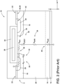
- FIG. 1 illustrates an active cell of a conventional planar n-channel field-effect transistor, such as a DMOSFET, hereinafter MOSFET device 10.
- MOSFET device 10 a conventional planar n-channel field-effect transistor, such as a DMOSFET, hereinafter MOSFET device 10. It may be appreciated that, in order to more clearly illustrate and describe certain components of the MOSFET device 10, as well as other devices discussed hereinbelow, certain commonly understood design elements (e.g., top metallization, passivation, edge termination, and so forth) may be omitted.
- the illustrated conventional MOSFET device 10 of FIG. 1 includes a semiconductor layer 2 (e.g., an epitaxial SiC semiconductor layer) having a first surface 4 and a second surface 6.
- the semiconductor layer 2 includes a drift region 16 having a first conductivity type (e.g., an n-type drift region 16), a well region 18 having a second conductivity type (e.g., a p-well region 18) disposed adjacent to the drift region 16 and proximal to the first surface 4.
- the semiconductor layer 2 also includes a source region 20 having the first conductivity type (e.g., an n-type source region 20) adjacent to the well region 18 and proximal to the first surface 4.
- a dielectric layer 24 (also referred to as a gate insulating layer or gate dielectric layer) is disposed on a portion of the first surface 4 of the semiconductor layer 2, and a gate electrode 26 is disposed on the dielectric layer 24.
- the second surface 6 of the semiconductor layer 2 is a substrate layer 14 (e.g., a SiC substrate layer), and the drain contact 12 is disposed on the bottom of the MOSFET device 10 along the substrate layer 14.
- a source contact 22 is disposed on top of the semiconductor layer 2, partially covering source region 20 and well region 18.
- an appropriate gate voltage e.g., at or beyond a threshold voltage (V TH ) of the MOSFET device 10) can cause an inversion layer to be formed in a channel region 28, as well as a conductive path to be enhanced in a junction field-effect transistor (JFET) region 29 due to accumulation of carriers, allowing current to flow from the drain contact 12 (i.e., the drain electrode) to the source contact 22 (i.e., the source electrode).
- the channel region 28 may be generally defined as an upper portion of the well region 18 disposed below the gate electrode 26 and the dielectric layer 24.
- FIG. 2 is a schematic cross-sectional view of the conventional MOSFET device 10 of FIG. 1 .
- the source contacts 22 of the MOSFET device 10 illustrated in FIG. 2 generally provide an ohmic connection to the source electrode, and are disposed over both a portion of the source regions 20 and a portion of the well regions 18.
- the source contact 22 is generally a metallic interface comprising one or more metal layers situated between these semiconductor portions of the MOSFET device 10 and the metallic source electrode.
- the portion of the source region 20 (e.g., an n+ source region 20) of the MOSFET device 10 disposed below the source contact 22 may be more specifically referred to herein as a source contact region 42 of the MOSFET device 10.
- a portion of the well region 18 (e.g., a p-well region 18) of the MOSFET device 10, which may be p+ doped at a higher level than the remainder of the well region 18, may be more specifically referred to herein as a body region 44 (e.g., p+ body region 44) of the MOSFET device 10.
- a body contact region 44 e.g., p+ body contact region 44
- portions of the source contact 22 may be designated herein based on the portion of the semiconductor device that is disposed below the source contact 22.
- the portion of the source contact 22 disposed above a body contact region 44 may be referred to herein as the body contact portion of the source contact 22.
- the portion of the source contact 22 disposed above a source contact region 42 of the MOSFET device 10 may be referred to herein as a source contact portion of the source contact 22.
- the various regions of the MOSFET device 10 may each have an associated resistance, and a total resistance (e.g., an on-state resistance, Rds(on)) of the MOSFET device 10, which may be represented as a sum of each of these resistances.
- on-state resistance, Rds(on) of the MOSFET device 10 may be approximated as a sum of: a resistance Rs 30 (e.g., a resistance of source region 20 and a resistance of the source contact 22); a resistance Rch 32 (e.g., an inversion channel resistance of the channel region 28 illustrated in FIG.
- a resistance Race 34 e.g., a resistance of an accumulation layer between the dielectric layer 24 and portion of drift region 16 located between well regions 18
- a resistance RJFET 36 e.g., resistance of undepleted neck region between well regions 18
- a resistance Rdrift 38 e.g., the resistance about the drift region 16
- a resistance Rsub 40 e.g., the resistance about the substrate layer 14
- one or two resistance components illustrated in FIG. 2 may dominate conduction losses of the MOSFET device 10, and addressing these factors can significantly impact Rds(on).
- the channel resistance (Rch 32) may account for a significant portion of device conduction losses.
- JFET region resistance may account for a significant portion of total conduction losses.
- the MOSFET channel and JFET can comprise approximately 55% of a typical semiconductor device on-state resistance.
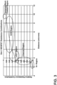
- FIG. 3 a chart depicting an example of the relative resistance contributions of the various regions of the MOSFET device structure of FIG. 2 is illustrated.
- the relative resistance for each region is depicted as a function of the respective region distance (e.g., path length).
- the inversion channel resistance Rch 32 of the channel region 28 can be the largest contributor to the on-state resistance Rds(on) of the MOSFET device 10, while the resistance Rs 30 (e.g., a resistance of source region 20 and a resistance of the source contact 22), and substrate or back contact region resistance Rsub 40 (e.g., the resistance about the substrate layer 14), contribute the least resistance to the on-state resistance Rds(on) of the MOSFET device 10.
- FIG. 4 illustrates a top-down view of a conventional semiconductor layer 2 including a MOSFET device structure 41 having a conventional stripe cell layout. (i.e., a non-cellular layout).
- the illustrated stripe layout of FIG. 4 includes: the channel regions 28, source regions 20, source contact regions 42, body contact regions 44, and JFET region 29. It may be appreciated that a set of source contact regions 42 and a set of body contact regions 44 can be formed as continuous stripes along the surface of the semiconductor for the illustrated stripe layout of FIG. 4 .
- the conventional MOSFET device structure 41 may be described as having a particular channel length (Lch) 43, a distance from channel region 28 to ohmic region (Lch-to-ohm) 45, a width of the ohmic region (Wohm 47), and a width of the JFET region (WJFET) 49. While the conventional stripe cell layout illustrated in FIG. 4 offers good reliability (e.g., long term and high temperature performance), the relatively high channel resistance (Rch) 32 and JFET resistance (RJFET) 36 of the MOSFET device structure 41 results in a relatively high Rds(on), which diminishes the electrical performance of the device.
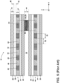
- FIG. 5 is a top-down or plan view of a stripe ladder device layout 50 (i.e., a non-cellular layout) with segmented source/body contacts.
- the illustrated stripe ladder device layout 50 includes: channel regions 28, source regions 20, a set of segmented source/body contacts 46 (including a body contact region 44 and the source contact region 42) and JFET region 29.
- FIG. 5 is a top-down or plan view of a stripe ladder device layout 50 (i.e., a non-cellular layout) with segmented source/body contacts.
- the illustrated stripe ladder device layout 50 includes: channel regions 28, source regions 20, a set of segmented source/body contacts 46 (including a body contact region 44 and the source contact region 42) and JFET region 29.
- FIG. 5 is a top-down or plan view of a stripe ladder device layout 50 (i.e., a non-cellular layout) with segmented source/body contacts.
- the illustrated stripe ladder device layout 50 includes: channel regions 28, source regions
- FIG. 5 further illustrates dimensions of the stripe ladder device layout 50, including: channel length (Lch) 43, distance from the channel to the ohmic region (Lch-to-ohm) 45, width of the ohmic region (Wohm) 47, width of the JFET region (WJFET) 49, length of the source contact region segment (Ln) 51, length of the body contact region segment (Lp) 52, subset of device area (Acell 53 represented by the dashed rectangle 53), JFET area within Acell 53 (ANET 54 represented by the cross-hatched area 54), and width of the channel (Wch) 55 within Acell 54 for the illustrated stripe ladder device layout 50.
- channel length (Lch) 43 distance from the channel to the ohmic region (Lch-to-ohm) 45
- width of the ohmic region (Wohm) 47 width of the JFET region (WJFET) 49
- length of the source contact region segment (Ln) 51 length of the body contact region segment (
- FIG. 6 is a top-down or plan view of a square cellular device layout 60 that does not include segmented source/body contacts.
- the square cellular device layout 60 includes: channel regions 28, source regions 20, body contact region 44, source contact 22, and JFET regions 29.
- FIG. 6 is a top-down or plan view of a square cellular device layout 60 that does not include segmented source/body contacts.
- the square cellular device layout 60 includes: channel regions 28, source regions 20, body contact region 44, source contact 22, and JFET regions 29.
- FIG. 6 further illustrates dimensions of the square cellular device layout 60, including: channel length (Lch 62), distance from the channel to the ohmic region (Lch-to-ohm) 63, width of the ohmic region (Wohm) 64, width of the JFET region (WJFET) 65, width of the body contact region (Wp) 67, device cell area (Acell represented by the dashed rectangle 68), JFET area per cell (AJFET) represented by the cross-hatched area 69, for the illustrated cell of the square cellular device layout 60.
- the device layouts illustrated in FIG. 6 may enable lower Rds(on) relative to a stripe cell layout, as illustrated in FIG. 3 , it is recognized that such designs can have a substantially higher electric field in portions of the JFET region 29 between the corners of the well regions 18 of neighboring device cells under blocking conditions.
- the electric field in the dielectric layer 24 e.g., SiO2
- the dielectric layer 24 can be around ten times higher compared to that in Si devices when the device cells operate under reverse bias.
- SiC is generally robust toward higher electric fields, the dielectric layer 24 may experience breakdown during long term operation, resulting in reliability issues with the SiC device cells.
- present embodiments are directed toward semiconductor device designs and layouts that enable improved semiconductor device performance.
- aspects as described herein can advantageously reduce the resistance of the components of the MOSFET device.
- non-limiting aspects can include cellular device designs and layouts that provide increased channel width or increased channel density over conventional designs to reduce the channel resistance (Rch 32) and, thereby, reduce on-state conduction losses.
- channel density can refer to the ratio of the length of a channel periphery of a particular device cell to the total area of the device cell.
- the channel density may be equal to the total channel perimeter of one device cell divided by the area of the device cell.
- the non-limiting aspect as described herein enable the reduction of device pitch, and thus, increases channel periphery per unit area or increases density of the channel region 28 for the MOSFET device.
- FIG. 7 depicts a top-down or plan view illustrating a system 70 (e.g., a cellular semiconductor device such as a MOSFET) comprising an array of semiconductor device cells 72 in accordance with a non-limiting aspect.
- the semiconductor device cells 72 can be configured to enable a reduced on-state resistance Rds(on) of the MOSFET device 10.
- Each semiconductor device cell 72 can be disposed at the first surface 4 of a semiconductor layer 2 (e.g., a silicon carbide (SiC) semiconductor layer).
- the semiconductor device cell 72 can define a vertical pitch or first axial length D 1 extending across the extent of the first surface 4 of the semiconductor device cell 72, for example along the x-axis.
- the semiconductor device cell 72 can also define a horizontal pitch or second axial length D2 extending across the extent of the first surface 4 of the semiconductor device cell 72 orthogonal to the first axial length D1, for example along the y-axis. It will be appreciated that an area of the semiconductor device cell 72 can be determined based on the product of first axial length D 1 and the second axial length D2.
- the body contact region 44 of the semiconductor device cell 72 can be surrounded by a source region 20 of the first conductivity type (e.g. an n-type. or a p-type. A periphery of the source region 20 can be surrounded by a well region 18 of the second conductivity type. It may be appreciated that, portions of the source region 20 disposed below the source contact 22 serve as portions of the source contact region 42 of the semiconductor device cell 72.
- the semiconductor device cell 72 can include a drift region 16 having the first conductivity type.
- a well region 18 having a second conductivity type can be disposed adjacent to the drift region 16.
- the well region 18 can comprise a set of elongate well region segments 17 spaced from each other.
- Each well region segment 17 can define a respective well region segment longitudinal axis 17a.
- the respective well region segment longitudinal axes 17a can extend across the first surface 4, for example along the x-axis.
- two or more well region segment longitudinal axes 17a can be generally parallel with each other.
- the well region segment longitudinal axes 17a can be generally parallel with the first axial length D1.
- the source region 20 can be disposed immediately adjacent to the well region 18 and surrounded by the well region 18.
- a channel region 28 having the second conductivity type can be disposed proximal to the first surface 4.
- the channel region 28 can comprise a set of elongate channel region segments 28a spaced from each other.
- the channel region segments 28a can define a periphery of the channel region 28.
- Each channel region segment 28a can define a respective channel region segment longitudinal axis 31.
- the respective channel region segment longitudinal axes 31 can extend across the first surface 4, for example along the x-axis. In this sense, the respective channel region segment longitudinal axes 31 can be parallel to the first axial length D1.
- two or more channel region segment longitudinal axes 31 can be generally parallel with each other.
- two or more channel region segment longitudinal axes 31 can be generally parallel with two or more well region segment longitudinal axes 17a.
- a pair of immediately adjacent channel region segments 28a can be spaced apart from one another along their respective longitudinal axes 31, to define a gap 33 therebetween.
- Each gap 33 can define a respective third axial length D3 orthogonal to the respective channel region segment longitudinal axes 31.
- the third axial length D3 can be substantially orthogonal to the first axial length D1.
- a respective well region segment 17 can be disposed within the gap 33, and the well respective well region segment longitudinal axis 17a can be parallel to the respective channel region segment longitudinal axes 31.
- the channel region segments 28a can be at least partially surrounded by the well region 18.
- a periphery of the channel region segments 28a can be cooperatively surrounded by a respective well region segment 17 and the drift region 16.
- a periphery of the set of channel region segments 28a, the set of well region segments 17, and portions of the field-effect transistor (JFET) region 29 can be arranged to define a series of alternating substantially parallel elongate bands or stripes.
- JFET field-effect transistor
- the body contact region 44 having the second conductivity type can be disposed over a portion of the well region 18. In non-limiting aspects, the body contact region 44 can be disposed substantially in the center of a plane of the source region 20 defined by the first surface 4.
- the well region 18, source region 20, and channel region 28 can cooperatively or cumulatively define the first axial length D1 or pitch extending across the first surface 4 of the semiconductor device cell 72.
- the first axial length D1 can be substantially parallel with the channel region segment longitudinal axes 31 or the well region segment longitudinal axes 17a, or both.
- the first axial length D1 can span substantially an entire length of the first surface 4 of the semiconductor device cell 72.
- each well region segment 17 can define the respective third axial length D3 or pitch extending across the surface 4, for example along the y-axis.
- the third axial length D3 can be arranged orthogonal to the first axial length D 1.
- the first axial length D1 can be within the range of 6 microns and 18 microns.
- the third axial length D3 can be within the range of 0.3 microns to 1.6 microns.
- the relative dimensions of the first and third axial lengths D1, D3, the third axial length D3 can be within the range of between 5% - 20% of the first axial length D1.
- Other aspects are not so limited, and the dimensions of the first axial length D 1, or the third axial length D3, or both, can vary as desired for various applications without departing from the scope of the disclosure herein.
- the specific dimensions the first and third axial lengths D1, D3 are arranged or defined with the particular purpose of decreasing the resistance contribution of the channel region 28 (i.e. the relatively higher resistance contribution of the inversion channel resistance), even at the expense of a relatively smaller consequent increase in the resistance contribution of the well region 18.
- FIG. 8 depicts a top-down or plan view illustrating an array of a system 80 including semiconductor device cells 72 in accordance with another non-limiting aspect.
- the non-limiting aspect of FIG. 8 is similar to the aspect depicted in FIG. 7 , with one difference being that semiconductor device cells 72 are arranged in a cellular type layout.
- FIG. 9 depicts a cross-sectional view of the semiconductor device cells 72 of FIG. 8 taken along the line IX-IX.
- the semiconductor device cells 72 are configured to enable a reduced on-state resistance Rds(on) of the system 80.
- Each semiconductor device cell 72 is disposed at the first surface 4 of a semiconductor layer 2 (e.g., a SiC semiconductor layer 2).
- the semiconductor device cell 72 can define the vertical pitch or first axial length D1 extending across the extent of the first surface 4 of the semiconductor device cell 72, for example along the x-axis.
- the dielectric layer 24 (e.g., the gate insulating layer) is disposed on a portion of the first surface 4 of the semiconductor layer 2, and the gate electrode 26 is disposed on the dielectric layer 24.
- the body contact region 44 of the semiconductor device cell 72 is surrounded by the source region 20 of the first conductivity type (e.g. an n-type. or a p-type).
- a periphery of the source region 20 of the first conductivity type can be surrounded by a well region 18 of the second conductivity type. Portions of the source region 20 disposed below the source contact 22 can serve as portions of the source contact region 42 of the semiconductor device cell 72.
- the semiconductor device cell 72 can include the drift region 16 having the first conductivity type.
- the well region 18 having a second conductivity can be disposed adjacent to the drift region 16.
- the well region 18 can comprise the set of elongate well region segments 17 spaced from each other and defining the respective well region segment longitudinal axes 17a.
- each well region segment longitudinal axis 17a can be generally parallel with each other.
- the well region segment longitudinal axes 17a can be generally parallel with the first axial length D1.
- the source region 20 is disposed immediately adjacent to the well region 18 and surrounded by the well region 18.
- the channel region 28 having the second conductivity type can be disposed proximal to the first surface 4.
- the channel region 28 comprises a set of elongate channel region segments 28a spaced from each other and defining a respective channel region segment longitudinal axis 31.
- each channel region segment longitudinal axis 31 can be generally parallel with each other.
- the respective channel region segment longitudinal axes 31 can extend across the first surface 4, for example along the x-axis. In this sense, the respective channel region segment longitudinal axes 31 can be parallel to the first axial length D1. Additionally, in some aspects, each channel region segment longitudinal axis 31 can be generally parallel with the well region segment longitudinal axes 17a.
- one or more respective channel region segments 28a can be spaced apart from another immediately adjacent channel region segment 28a to define a gap 33 therebetween.
- Each gap 33 can define a respective third axial length D3 orthogonal to the respective channel region segment longitudinal axes 31.
- the third axial length D3 can be substantially orthogonal to the first axial length D 1.
- a respective well region segment 17 can be disposed within the gap 33, such that the respective well region segment longitudinal axis 17a can be parallel to the respective channel region segment longitudinal axes 31.
- a periphery of the channel region segments 28a can be at least partially surrounded by the well region 18.
- the channel region segments 28a can be cooperatively surrounded by a respective well region segment 17 and the drift region 16.
- the set of channel region segments 28a, the set of well region segments 17, and portions of the drift region 16 can be arranged to define a series of alternating substantially parallel bands or stripes.
- the semiconductor device cell 72 may be described as having the well region segments 17 disposed on opposite sides of the channel region segments 28a.
- the body contact region 44 having the second conductivity type can be disposed over a portion of the well region 18.
- the body contact region 44 can be disposed substantially in the center of a plane of the source region 20 defined by the first surface 4.
- the well region 18, source region 20, and channel region 28 can cooperatively or cumulatively define the first axial length D1 or pitch extending across the first surface 4 of the semiconductor device cell 72.
- the first axial length D1 can be substantially parallel with the channel region segment longitudinal axes 31 or the well region segment longitudinal axes 17a, or both.
- the first axial length D1 can span substantially an entire length of the first surface 4 of the semiconductor device cell 72.
- each well region segment 17 can define the respective third axial length D3 or pitch extending across the surface 4, for example along the y-axis.
- the third axial length D3 can be arranged orthogonal to the first axial length D 1.
- the first axial length D1 can be within the range of 6 microns and 18 microns.
- the third axial length D3 can be within the range of 0.3 microns to 1.6 microns.
- the relative dimensions of the first and third axial lengths D1, D3, the third axial length D3 can be within the range of 5% - 20% of the first axial length D1.
- Other aspects are not so limited, and the dimensions of the first axial length D 1, or the third axial length D3, or both, can vary as desired for various applications without departing from the scope of the disclosure herein.
- the specific dimensions the first and third axial lengths D1, D3 are arranged or defined with the particular purpose of decreasing the resistance contribution of the channel region 28 (i.e. the relatively higher resistance contribution of the inversion channel resistance), even at the expense of a relatively smaller consequent increase in the resistance contribution of the well region 18.
- the illustrated semiconductor device cell 72 may be described as having portions of the well region 18 disposed on opposite sides of the channel region segments 28a. Thus, non-limiting aspects can minimize cell size and increase the density of the conducting channel region 28 per unit cell.
- the presently disclosed semiconductor device cell 72 minimizes cell size and increases density of conducting regions (e.g., channel) per unit cell.
- present aspects reduce device conduction losses (e.g., minimize Rds(on)) by providing increased channel width and/or increased channel density to reduce the channel resistance.
Landscapes
- Electrodes Of Semiconductors (AREA)
- Insulated Gate Type Field-Effect Transistor (AREA)
- Bipolar Transistors (AREA)
- Semiconductor Memories (AREA)
Abstract
Description
- Semiconductor devices, such as silicon carbide (SiC) power devices, are widely used in conventional electrical systems to switch or convert electrical power for consumption by a load. Many electronics systems utilize various semiconductor devices and components, such as thyristors, diodes, and various types of transistors (e.g., metal-oxide-semiconductor field-effect transistor (MOSFETs), insulated gate bipolar transistors (IGBTs), and other suitable transistors). For example, MOSFETs can be fabricated as discrete transistor packages for high power applications, or as chips with millions of transistors. Many thousands of these transistor "cells" can be combined into one device in order to handle relatively high currents and voltages.
- Many conventional MOSFETs use a vertical structure with source and drain terminals at opposite sides of a chip. The vertical orientation eliminates crowding at the gate and offers larger channel widths. Generally, when a semiconductor device is conducting current, the on-state resistance of the device represents its conduction loss, which impacts the efficiency of the device and its cost. That is, conventional semiconductor device cells include a number of internal components that can create resistance to the current flowing through the device.
- In the drawings:
-
FIG. 1 is a schematic of a typical planar MOSFET device. -
FIG. 2 is a schematic illustrating resistance for various regions of a typical MOSFET device. -
FIG. 3 is a chart depicting the relative resistance contributions of the regions of the MOSFET device structure ofFIG. 2 . -
FIG. 4 is a top-down view of a surface of a SiC layer that includes a typical MOSFET device structure having a stripe cell layout. -
FIG. 5 is a top-down view of a surface of a SiC layer that includes a typical MOSFET device structure having a stripe cell layout. -
FIG. 6 is a top-down view of a surface of a SiC layer that includes a typical MOSFET device structure having a cellular layout. -
FIG. 7 is a top-down view of a system comprising an array of semiconductor device cells in in accordance with various aspects described herein. -
FIG. 8 is a top-down view of a system comprising an alternative array of semiconductor device cells in accordance with various aspects described herein. -
FIG. 9 is a cross-sectional view of the semiconductor device cells ofFIG. 8 . - Aspects of the disclosure can be implemented in any environment, apparatus, or method for cooling a heat-generating module regardless of the function performed by the heat-generating module.
- As used herein, the term "set" or a "set" of elements can be any number of elements, including only one. When introducing elements of various embodiments of the present disclosure, the articles "a," "an," and "the" are intended to mean that there are one or more of the elements. The terms "comprising," "including," and "having" are intended to be inclusive and mean that there may be additional elements other than the listed elements. Additionally, it should be understood that references to "one aspect" or "an aspect" of the present disclosure are not intended to be interpreted as excluding the existence of additional aspects that also incorporate the recited features. It may be appreciated that the shapes, positions, and alignments of features presently disclosed are, for the sake of simplicity, illustrated and described as being relatively ideal (e.g., square, rectangular, and hexagonal cells and shielding regions with perfectly straight and aligned features). However, as may be appreciated by one of skill in the art, process variations and technical limitations may result in cellular designs with less than ideal shapes or irregular features may still be in accordance with the present disclosure. As such, the term "substantially" as used herein to describe a shape, a position, or an alignment of a feature is meant to encompass ideal or target shapes, positions, and alignments as well as imperfectly implemented shapes, positions, and alignments resulting from variability in the semiconductor fabrication process, as may be appreciated by one skilled in the art.
- Additionally, semiconductor device cells are described herein as being disposed or fabricated "at the surface," "in the surface," "on the surface," or "along the surface" of a semiconductor layer, which is intended to include semiconductor device cells having portions disposed within the bulk of the semiconductor layer, portions disposed proximate to the surface of the semiconducting layer, portions disposed even with the surface of the semiconductor layer, and/or portions disposed above or on top of the surface of the semiconductor layer.
- While terms such as "voltage", "current", and "power" can be used herein, it will be evident to one skilled in the art that these terms can be interrelated when describing aspects of the electrical circuit, or circuit operations.
- All directional references (e.g., radial, axial, upper, lower, upward, downward, left, right, lateral, front, back, top, bottom, above, below, vertical, horizontal, clockwise, counterclockwise) are only used for identification purposes to aid the reader's understanding of the disclosure, and do not create limitations, particularly as to the position, orientation, or use thereof. Connection references (e.g., attached, coupled, connected, and joined) are to be construed broadly and can include intermediate members between a collection of elements and relative movement between elements unless otherwise indicated. As such, connection references do not necessarily infer that two elements are directly connected and in fixed relation to each other. In non-limiting examples, connections or disconnections can be selectively configured to provide, enable, disable, or the like, an electrical connection between respective elements. The exemplary drawings are for purposes of illustration only and the dimensions, positions, order and relative sizes reflected in the drawings attached hereto can vary.
- As used herein, a controllable switching element, or a "switch" is an electrical device that can be controllable to toggle between a first mode of operation, wherein the switch is very low resistance state or in an "ON" state, or otherwise in a conducting mode, intending to transmit current from a switch input to a switch output, and a second mode of operation, wherein the switch is very high resistance state or in an OFF state, or otherwise in a non-conducting mode, intending to prevent current from transmitting between the switch input and switch output. In non-limiting examples, connections or disconnections, such as connections enabled or disabled by the controllable switching element, can be selectively configured to provide, enable, disable, or the like, an electrical connection between respective elements.
- Furthermore, for ease of description and understanding, while various aspects may be discussed below in the context of SiC MOSFET devices, it should be appreciated the present approach may be applicable to other types of MOSFETS, such as, but not limited to SiC DMOSFETs, UMOSFETs, and VMOSFETs. It is contemplated that various material systems (e.g., silicon (Si), germanium (Ge), aluminum nitride (AlN), gallium nitride (GaN), gallium arsenide (GaAs), diamond (C), or any other suitable wide band-gap semiconductor) can be used. It is further contemplated that other types of device structures (e.g., UMOSFET, VMOSFETs, insulated gate bipolar transistors (IGBT), insulated base MOS-controlled thyristors (IBMCT), or any other suitable FET and/or MOS device)) utilizing n-channel or p-channel designs can be used in various non-limiting aspects.
- One of the most common solid-state semiconductor switching devices used in modern power electronics is the MOSFET device. While an ideal switch would conduct electrical current with zero electrical resistance when in a low resistance "ON" or conducting state, a MOSFET will always exhibit a finite electrical resistance. Thus, it is generally desirable to reduce the total resistance (e.g., an on-state resistance) to the minimum possible value. It is also desirable to minimize the ON-state resistance of the MOSFET, without reducing the OFF-state resistance, the switching speed of the device, or both.
- Conventional MOSFETs typically consist of arrays of periodic unit cells. Each unit cell can have a respective electrical resistance, and the MOSFET on-state electrical resistance can be defined by the sum of the respective cell resistances in a parallel electrical circuit. Additionally, each unit cell resistance can be defined by a set of respective resistance values of the structural components of the cell coupled in series. The on-state resistance of a particular MOSFET can thus be defined based at least in part on the relative geometric structures of the various functional components within the respective cells.
- When a MOSFET is in an ON or conducting state, electrons flow through each individual cell from a "source metal" on the top surface of a SiC semiconductor body, through various structures defined within the SiC semiconductor body, and into a "drain metal" on the back surface of the body. Each respective MOSFET unit cell surface can include four mutually exclusive, non-overlapping regions referred to herein as the source contact region, the n+/p-well region, and the channel /accumulation region (CHAN) and the JFET region. The four regions can be coupled electrically in series, and can occupy substantially the entire area of the respective cell.
- The resistive contributions of the source contact and the CHAN regions to the on-state electrical resistance of the MOSFET are inversely proportional to their respective areas. The resistive contribution of the n+/p-well region to the on-state electrical resistance of the MOSFET is roughly directly proportional to its area. Since the resistive contribution of the CHAN region is relatively greater than that of the n+/p-well, or the source contact region, the on-state electrical resistance of the MOSFET can be reduced by maximizing the relative area of the CHAN region in the unit cell with respect to the n+/p-well, or the source contact region. Thus, conventional techniques typically employ MOSFET structures with a maximized relative proportion of the CHAN region area by arranging the cell geometries to minimize the relative proportion of the n+/p-well region area, or the source contact region area, or both, with respect to the CHAN region.
- However, for SiC MOSFETs, current fabrication technology can limit such optimization. For example, conventional techniques have focused on reducing MOSFET on-state resistance using periodic cells produced by surrounding a minimum size source contact region with a minimum size n+ region, relative to the CHAN region. However, the minimum fabricable source contact region dimensions (using conventional fabrication techniques) can be larger than a calculated or determined optimized area. Furthermore, the CHAN region must be separated from the source contact region by a minimum width of the n+/p-well region to avoid fabrication-related device failure. Notably, however, the geometry of the n+/p- well region is relatively unconstrained by such fabrication concerns.
- Accordingly, as described in more detail herein, in non-limiting aspects, the cells can be arranged to minimize the relative proportion of the n+/p-well region area, while minimally increasing the source contact region area and the CHAN region area. In this way, aspects as described herein can thereby arrange a greater net relative proportion of the CHAN region area with respect to the source contact region or size n+ region, or both, compared to conventional techniques, and thereby achieve an improved (i.e., lower) on-state resistance for the respective cell than conventional devices.
- For example, non-limiting aspects can employ a cellular structure comprising an array of cells spaced further apart than conventional devices. The resultant increased space or area between adjacent cells can comprise alternating bands or segments of n+/p-well and CHAN regions. With this novel arrangement, the relative proportion of the CHAN region with respect to the n+/p-well, or the source contact region, or both, can advantageously be increased beyond the level achievable using conventional techniques that increase the relative proportion of the CHAN area by minimizing the n+/p-well, or the source contact region, or combinations thereof. As will be described in more detail herein, an undesirable increase in on-state resistance resulting from the increased area of the n+/p-well region (e.g., in the alternating bands), can be negated or overcome within a predetermined dimensional range, due to the decrease in on-state resistance achieved by the corresponding increased area of the CHAN region, thereby resulting in a net decrease in the on-state resistance of the respective cell compared to conventional designs.
-
FIG. 1 illustrates an active cell of a conventional planar n-channel field-effect transistor, such as a DMOSFET, hereinafterMOSFET device 10. It may be appreciated that, in order to more clearly illustrate and describe certain components of theMOSFET device 10, as well as other devices discussed hereinbelow, certain commonly understood design elements (e.g., top metallization, passivation, edge termination, and so forth) may be omitted. - The illustrated
conventional MOSFET device 10 ofFIG. 1 includes a semiconductor layer 2 (e.g., an epitaxial SiC semiconductor layer) having afirst surface 4 and asecond surface 6. Thesemiconductor layer 2 includes adrift region 16 having a first conductivity type (e.g., an n-type drift region 16), awell region 18 having a second conductivity type (e.g., a p-well region 18) disposed adjacent to thedrift region 16 and proximal to thefirst surface 4. Thesemiconductor layer 2 also includes asource region 20 having the first conductivity type (e.g., an n-type source region 20) adjacent to thewell region 18 and proximal to thefirst surface 4. A dielectric layer 24 (also referred to as a gate insulating layer or gate dielectric layer) is disposed on a portion of thefirst surface 4 of thesemiconductor layer 2, and agate electrode 26 is disposed on thedielectric layer 24. Thesecond surface 6 of thesemiconductor layer 2 is a substrate layer 14 (e.g., a SiC substrate layer), and thedrain contact 12 is disposed on the bottom of theMOSFET device 10 along thesubstrate layer 14. Asource contact 22 is disposed on top of thesemiconductor layer 2, partially coveringsource region 20 andwell region 18. - During on-state operation, an appropriate gate voltage (e.g., at or beyond a threshold voltage (VTH) of the MOSFET device 10) can cause an inversion layer to be formed in a
channel region 28, as well as a conductive path to be enhanced in a junction field-effect transistor (JFET)region 29 due to accumulation of carriers, allowing current to flow from the drain contact 12 (i.e., the drain electrode) to the source contact 22 (i.e., the source electrode). It should be appreciated that, for the MOSFET devices discussed herein, thechannel region 28 may be generally defined as an upper portion of thewell region 18 disposed below thegate electrode 26 and thedielectric layer 24. -
FIG. 2 is a schematic cross-sectional view of theconventional MOSFET device 10 ofFIG. 1 . Thesource contacts 22 of theMOSFET device 10 illustrated inFIG. 2 generally provide an ohmic connection to the source electrode, and are disposed over both a portion of thesource regions 20 and a portion of thewell regions 18. Thesource contact 22 is generally a metallic interface comprising one or more metal layers situated between these semiconductor portions of theMOSFET device 10 and the metallic source electrode. For clarity, the portion of the source region 20 (e.g., an n+ source region 20) of theMOSFET device 10 disposed below thesource contact 22 may be more specifically referred to herein as asource contact region 42 of theMOSFET device 10. Similarly, a portion of the well region 18 (e.g., a p-well region 18) of theMOSFET device 10, which may be p+ doped at a higher level than the remainder of thewell region 18, may be more specifically referred to herein as a body region 44 (e.g., p+ body region 44) of theMOSFET device 10. For clarity, the portion of thebody region 44 that is disposed below (e.g., covered by, directly electrically connected to) thesource contact 22, may be more specifically referred to herein as a body contact region 44 (e.g., p+ body contact region 44) of theMOSFET device 10. For consistency, portions of thesource contact 22 may be designated herein based on the portion of the semiconductor device that is disposed below thesource contact 22. For example, the portion of thesource contact 22 disposed above abody contact region 44 may be referred to herein as the body contact portion of thesource contact 22. Similarly, the portion of thesource contact 22 disposed above asource contact region 42 of theMOSFET device 10 may be referred to herein as a source contact portion of thesource contact 22. - As illustrated schematically in
FIG. 2 , the various regions of theMOSFET device 10 may each have an associated resistance, and a total resistance (e.g., an on-state resistance, Rds(on)) of theMOSFET device 10, which may be represented as a sum of each of these resistances. For example, as illustrated inFIG. 2 , on-state resistance, Rds(on), of theMOSFET device 10 may be approximated as a sum of: a resistance Rs 30 (e.g., a resistance ofsource region 20 and a resistance of the source contact 22); a resistance Rch 32 (e.g., an inversion channel resistance of thechannel region 28 illustrated inFIG. 2 ); a resistance Race 34 (e.g., a resistance of an accumulation layer between thedielectric layer 24 and portion ofdrift region 16 located between well regions 18); a resistance RJFET 36 (e.g., resistance of undepleted neck region between well regions 18); a resistance Rdrift 38 (e.g., the resistance about the drift region 16); and a resistance Rsub 40 (e.g., the resistance about the substrate layer 14). Note that the resistances illustrated inFIG. 2 are not intended to be exhaustive, and that other resistances (e.g., drain contact resistance, spreading resistance, etc.) could potentially be present within theMOSFET device 10. - In certain cases, one or two resistance components illustrated in
FIG. 2 may dominate conduction losses of theMOSFET device 10, and addressing these factors can significantly impact Rds(on). For example, for devices in which thedrift resistance 38, thesubstrate resistance 40 and the contact resistance are negligible, such as low-voltage devices or devices suffering from low inversion layer mobility (e.g. SiC devices), the channel resistance (Rch 32) may account for a significant portion of device conduction losses. - By further example, in medium-voltage and high-voltage devices, JFET region resistance (RJFET 36) may account for a significant portion of total conduction losses. In some cases, the MOSFET channel and JFET can comprise approximately 55% of a typical semiconductor device on-state resistance.
- With reference to
FIG. 3 , a chart depicting an example of the relative resistance contributions of the various regions of the MOSFET device structure ofFIG. 2 is illustrated. The relative resistance for each region is depicted as a function of the respective region distance (e.g., path length). It can be seen that the inversionchannel resistance Rch 32 of thechannel region 28 can be the largest contributor to the on-state resistance Rds(on) of theMOSFET device 10, while the resistance Rs 30 (e.g., a resistance ofsource region 20 and a resistance of the source contact 22), and substrate or back contact region resistance Rsub 40 (e.g., the resistance about the substrate layer 14), contribute the least resistance to the on-state resistance Rds(on) of theMOSFET device 10. -
FIG. 4 illustrates a top-down view of aconventional semiconductor layer 2 including a MOSFET device structure 41 having a conventional stripe cell layout. (i.e., a non-cellular layout). The illustrated stripe layout ofFIG. 4 includes: thechannel regions 28,source regions 20,source contact regions 42,body contact regions 44, andJFET region 29. It may be appreciated that a set ofsource contact regions 42 and a set ofbody contact regions 44 can be formed as continuous stripes along the surface of the semiconductor for the illustrated stripe layout ofFIG. 4 . In terms of dimensions, the conventional MOSFET device structure 41 may be described as having a particular channel length (Lch) 43, a distance fromchannel region 28 to ohmic region (Lch-to-ohm) 45, a width of the ohmic region (Wohm 47), and a width of the JFET region (WJFET) 49. While the conventional stripe cell layout illustrated inFIG. 4 offers good reliability (e.g., long term and high temperature performance), the relatively high channel resistance (Rch) 32 and JFET resistance (RJFET) 36 of the MOSFET device structure 41 results in a relatively high Rds(on), which diminishes the electrical performance of the device. - An example of another conventional device layout is illustrated in
FIG. 5 , which is a top-down or plan view of a stripe ladder device layout 50 (i.e., a non-cellular layout) with segmented source/body contacts. The illustrated stripeladder device layout 50 includes:channel regions 28,source regions 20, a set of segmented source/body contacts 46 (including abody contact region 44 and the source contact region 42) andJFET region 29.FIG. 5 further illustrates dimensions of the stripeladder device layout 50, including: channel length (Lch) 43, distance from the channel to the ohmic region (Lch-to-ohm) 45, width of the ohmic region (Wohm) 47, width of the JFET region (WJFET) 49, length of the source contact region segment (Ln) 51, length of the body contact region segment (Lp) 52, subset of device area (Acell 53 represented by the dashed rectangle 53), JFET area within Acell 53 (ANET 54 represented by the cross-hatched area 54), and width of the channel (Wch) 55 within Acell 54 for the illustrated stripeladder device layout 50. - For further comparison, another example of a conventional device layout is illustrated in
FIG. 6 , which is a top-down or plan view of a squarecellular device layout 60 that does not include segmented source/body contacts. The squarecellular device layout 60 includes:channel regions 28,source regions 20,body contact region 44,source contact 22, andJFET regions 29.FIG. 6 further illustrates dimensions of the squarecellular device layout 60, including: channel length (Lch 62), distance from the channel to the ohmic region (Lch-to-ohm) 63, width of the ohmic region (Wohm) 64, width of the JFET region (WJFET) 65, width of the body contact region (Wp) 67, device cell area (Acell represented by the dashed rectangle 68), JFET area per cell (AJFET) represented by the cross-hatched area 69, for the illustrated cell of the squarecellular device layout 60. - While the device layouts illustrated in
FIG. 6 may enable lower Rds(on) relative to a stripe cell layout, as illustrated inFIG. 3 , it is recognized that such designs can have a substantially higher electric field in portions of theJFET region 29 between the corners of thewell regions 18 of neighboring device cells under blocking conditions. For SiC MOS devices, the electric field in the dielectric layer 24 (e.g., SiO2) disposed over the JFET region 29 (illustrated inFIGS. 1 and2 ) can be around ten times higher compared to that in Si devices when the device cells operate under reverse bias. While SiC is generally robust toward higher electric fields, thedielectric layer 24 may experience breakdown during long term operation, resulting in reliability issues with the SiC device cells. - With the foregoing in mind, present embodiments are directed toward semiconductor device designs and layouts that enable improved semiconductor device performance. In particular, to reduce or minimize device on-state conduction losses (e. g., minimize Rds(on)) aspects as described herein can advantageously reduce the resistance of the components of the MOSFET device. For example, non-limiting aspects can include cellular device designs and layouts that provide increased channel width or increased channel density over conventional designs to reduce the channel resistance (Rch 32) and, thereby, reduce on-state conduction losses. It may be appreciated that, as used herein, the term, "channel density" can refer to the ratio of the length of a channel periphery of a particular device cell to the total area of the device cell. As such, for the aspects described and illustrated herein, the channel density may be equal to the total channel perimeter of one device cell divided by the area of the device cell. As described in more detail below, the non-limiting aspect as described herein enable the reduction of device pitch, and thus, increases channel periphery per unit area or increases density of the
channel region 28 for the MOSFET device. -
FIG. 7 depicts a top-down or plan view illustrating a system 70 (e.g., a cellular semiconductor device such as a MOSFET) comprising an array ofsemiconductor device cells 72 in accordance with a non-limiting aspect. As described in more detail herein, thesemiconductor device cells 72 can be configured to enable a reduced on-state resistance Rds(on) of theMOSFET device 10. Eachsemiconductor device cell 72 can be disposed at thefirst surface 4 of a semiconductor layer 2 (e.g., a silicon carbide (SiC) semiconductor layer). Thesemiconductor device cell 72 can define a vertical pitch or first axial length D 1 extending across the extent of thefirst surface 4 of thesemiconductor device cell 72, for example along the x-axis. Thesemiconductor device cell 72 can also define a horizontal pitch or second axial length D2 extending across the extent of thefirst surface 4 of thesemiconductor device cell 72 orthogonal to the first axial length D1, for example along the y-axis. It will be appreciated that an area of thesemiconductor device cell 72 can be determined based on the product of first axial length D 1 and the second axial length D2. - In non-limiting aspects, the
body contact region 44 of thesemiconductor device cell 72 can be surrounded by asource region 20 of the first conductivity type (e.g. an n-type. or a p-type. A periphery of thesource region 20 can be surrounded by awell region 18 of the second conductivity type. It may be appreciated that, portions of thesource region 20 disposed below thesource contact 22 serve as portions of thesource contact region 42 of thesemiconductor device cell 72. Thesemiconductor device cell 72 can include adrift region 16 having the first conductivity type. - A
well region 18 having a second conductivity type (e.g. an p-type. or an n-type) can be disposed adjacent to thedrift region 16. In aspects, thewell region 18 can comprise a set of elongatewell region segments 17 spaced from each other. Eachwell region segment 17 can define a respective well region segmentlongitudinal axis 17a. For example, as illustrated, in some aspects the respective well region segmentlongitudinal axes 17a can extend across thefirst surface 4, for example along the x-axis. In non-limiting aspects, two or more well region segmentlongitudinal axes 17a can be generally parallel with each other. In non-limiting aspects, the well region segmentlongitudinal axes 17a can be generally parallel with the first axial length D1. Thesource region 20 can be disposed immediately adjacent to thewell region 18 and surrounded by thewell region 18. - A
channel region 28 having the second conductivity type can be disposed proximal to thefirst surface 4. Thechannel region 28 can comprise a set of elongatechannel region segments 28a spaced from each other. In non-limiting aspects, thechannel region segments 28a can define a periphery of thechannel region 28. Eachchannel region segment 28a can define a respective channel region segmentlongitudinal axis 31. As illustrated, in some aspects the respective channel region segmentlongitudinal axes 31 can extend across thefirst surface 4, for example along the x-axis. In this sense, the respective channel region segmentlongitudinal axes 31 can be parallel to the first axial length D1. In non-limiting aspects, two or more channel region segmentlongitudinal axes 31 can be generally parallel with each other. Additionally, in some aspects, two or more channel region segmentlongitudinal axes 31 can be generally parallel with two or more well region segmentlongitudinal axes 17a. In non-limiting aspects, a pair of immediately adjacentchannel region segments 28a can be spaced apart from one another along their respectivelongitudinal axes 31, to define agap 33 therebetween. Eachgap 33 can define a respective third axial length D3 orthogonal to the respective channel region segmentlongitudinal axes 31. In aspects, the third axial length D3 can be substantially orthogonal to the first axial length D1. In non-limiting aspects, a respectivewell region segment 17 can be disposed within thegap 33, and the well respective well region segmentlongitudinal axis 17a can be parallel to the respective channel region segmentlongitudinal axes 31. - Additionally, the
channel region segments 28a can be at least partially surrounded by thewell region 18. For example, in non-limiting aspects, a periphery of thechannel region segments 28a can be cooperatively surrounded by a respectivewell region segment 17 and thedrift region 16. As illustrated inFIG. 7 , a periphery of the set ofchannel region segments 28a, the set ofwell region segments 17, and portions of the field-effect transistor (JFET)region 29 can be arranged to define a series of alternating substantially parallel elongate bands or stripes. Thus, non-limiting aspects can increase the density of the conductingchannel region 28 per unit cell area over conventional techniques. - In non-limiting aspects, the
body contact region 44 having the second conductivity type can be disposed over a portion of thewell region 18. In non-limiting aspects, thebody contact region 44 can be disposed substantially in the center of a plane of thesource region 20 defined by thefirst surface 4. - In non-limiting aspects, the
well region 18,source region 20, andchannel region 28 can cooperatively or cumulatively define the first axial length D1 or pitch extending across thefirst surface 4 of thesemiconductor device cell 72. In non-limiting aspects, the first axial length D1 can be substantially parallel with the channel region segmentlongitudinal axes 31 or the well region segmentlongitudinal axes 17a, or both. In aspects, the first axial length D1 can span substantially an entire length of thefirst surface 4 of thesemiconductor device cell 72. In non-limiting aspects, eachwell region segment 17 can define the respective third axial length D3 or pitch extending across thesurface 4, for example along the y-axis. In non-limiting aspects, the third axial length D3 can be arranged orthogonal to the first axial length D 1. - In non-limiting aspects, the first axial length D1 can be within the range of 6 microns and 18 microns. In some non-limiting aspects, the third axial length D3 can be within the range of 0.3 microns to 1.6 microns. In still other non-limiting aspects, the relative dimensions of the first and third axial lengths D1, D3, the third axial length D3 can be within the range of between 5% - 20% of the first axial length D1. Other aspects are not so limited, and the dimensions of the first axial length D 1, or the third axial length D3, or both, can vary as desired for various applications without departing from the scope of the disclosure herein.
- Regardless of the dimensions, or relative dimensions with respect to each other, or both, of the first and third axial lengths D1, D3, the specific dimensions the first and third axial lengths D1, D3 are arranged or defined with the particular purpose of decreasing the resistance contribution of the channel region 28 (i.e. the relatively higher resistance contribution of the inversion channel resistance), even at the expense of a relatively smaller consequent increase in the resistance contribution of the
well region 18. -
FIG. 8 depicts a top-down or plan view illustrating an array of asystem 80 includingsemiconductor device cells 72 in accordance with another non-limiting aspect. The non-limiting aspect ofFIG. 8 is similar to the aspect depicted inFIG. 7 , with one difference being thatsemiconductor device cells 72 are arranged in a cellular type layout. Simultaneous reference will also be made toFIG. 9 which depicts a cross-sectional view of thesemiconductor device cells 72 ofFIG. 8 taken along the line IX-IX. - In the non-limiting aspect illustrated in
FIGS. 8 and9 , thesemiconductor device cells 72 are configured to enable a reduced on-state resistance Rds(on) of thesystem 80. Eachsemiconductor device cell 72 is disposed at thefirst surface 4 of a semiconductor layer 2 (e.g., a SiC semiconductor layer 2). Thesemiconductor device cell 72 can define the vertical pitch or first axial length D1 extending across the extent of thefirst surface 4 of thesemiconductor device cell 72, for example along the x-axis. - The dielectric layer 24 (e.g., the gate insulating layer) is disposed on a portion of the
first surface 4 of thesemiconductor layer 2, and thegate electrode 26 is disposed on thedielectric layer 24. Thebody contact region 44 of thesemiconductor device cell 72 is surrounded by thesource region 20 of the first conductivity type (e.g. an n-type. or a p-type). A periphery of thesource region 20 of the first conductivity type can be surrounded by awell region 18 of the second conductivity type. Portions of thesource region 20 disposed below thesource contact 22 can serve as portions of thesource contact region 42 of thesemiconductor device cell 72. Thesemiconductor device cell 72 can include thedrift region 16 having the first conductivity type. - The
well region 18 having a second conductivity can be disposed adjacent to thedrift region 16. In aspects, thewell region 18 can comprise the set of elongatewell region segments 17 spaced from each other and defining the respective well region segmentlongitudinal axes 17a. In non -limiting aspects, each well region segmentlongitudinal axis 17a can be generally parallel with each other. In non-limiting aspects, the well region segmentlongitudinal axes 17a can be generally parallel with the first axial length D1. Thesource region 20 is disposed immediately adjacent to thewell region 18 and surrounded by thewell region 18. - The
channel region 28 having the second conductivity type can be disposed proximal to thefirst surface 4. Thechannel region 28 comprises a set of elongatechannel region segments 28a spaced from each other and defining a respective channel region segmentlongitudinal axis 31. In non-limiting aspects, each channel region segmentlongitudinal axis 31 can be generally parallel with each other. In some aspects, the respective channel region segmentlongitudinal axes 31 can extend across thefirst surface 4, for example along the x-axis. In this sense, the respective channel region segmentlongitudinal axes 31 can be parallel to the first axial length D1. Additionally, in some aspects, each channel region segmentlongitudinal axis 31 can be generally parallel with the well region segmentlongitudinal axes 17a. - In non-limiting aspects, one or more respective
channel region segments 28a can be spaced apart from another immediately adjacentchannel region segment 28a to define agap 33 therebetween. Eachgap 33 can define a respective third axial length D3 orthogonal to the respective channel region segmentlongitudinal axes 31. In aspects, the third axial length D3 can be substantially orthogonal to the first axial length D 1. In non-limiting aspects, a respectivewell region segment 17 can be disposed within thegap 33, such that the respective well region segmentlongitudinal axis 17a can be parallel to the respective channel region segmentlongitudinal axes 31. A periphery of thechannel region segments 28a can be at least partially surrounded by thewell region 18. For example, in non-limiting aspects, thechannel region segments 28a can be cooperatively surrounded by a respectivewell region segment 17 and thedrift region 16. As illustrated inFIG. 8 , the set ofchannel region segments 28a, the set ofwell region segments 17, and portions of thedrift region 16 can be arranged to define a series of alternating substantially parallel bands or stripes. In this sense, as illustrated inFIG. 8 , thesemiconductor device cell 72 may be described as having thewell region segments 17 disposed on opposite sides of thechannel region segments 28a. Thus, non-limiting aspects can minimize cell size and increase the density of the conductingchannel region 28 per unit cell. - In some non-limiting aspects, the
body contact region 44 having the second conductivity type can be disposed over a portion of thewell region 18. Thebody contact region 44 can be disposed substantially in the center of a plane of thesource region 20 defined by thefirst surface 4. - In non-limiting aspects, the
well region 18,source region 20, andchannel region 28 can cooperatively or cumulatively define the first axial length D1 or pitch extending across thefirst surface 4 of thesemiconductor device cell 72. In non-limiting aspects, the first axial length D1 can be substantially parallel with the channel region segmentlongitudinal axes 31 or the well region segmentlongitudinal axes 17a, or both. In aspects, the first axial length D1 can span substantially an entire length of thefirst surface 4 of thesemiconductor device cell 72. In non-limiting aspects, eachwell region segment 17 can define the respective third axial length D3 or pitch extending across thesurface 4, for example along the y-axis. In non-limiting aspects, the third axial length D3 can be arranged orthogonal to the first axial length D 1. - In non-limiting aspects, the first axial length D1 can be within the range of 6 microns and 18 microns. In some non-limiting aspects, the third axial length D3 can be within the range of 0.3 microns to 1.6 microns. In still other non-limiting aspects, the relative dimensions of the first and third axial lengths D1, D3, the third axial length D3 can be within the range of 5% - 20% of the first axial length D1. Other aspects are not so limited, and the dimensions of the first axial length D 1, or the third axial length D3, or both, can vary as desired for various applications without departing from the scope of the disclosure herein.
- Regardless of the dimensions, or relative dimensions with respect to each other, or both, of the first and third axial lengths D1, D3, the specific dimensions the first and third axial lengths D1, D3 are arranged or defined with the particular purpose of decreasing the resistance contribution of the channel region 28 (i.e. the relatively higher resistance contribution of the inversion channel resistance), even at the expense of a relatively smaller consequent increase in the resistance contribution of the
well region 18. Additionally, the illustratedsemiconductor device cell 72 may be described as having portions of thewell region 18 disposed on opposite sides of thechannel region segments 28a. Thus, non-limiting aspects can minimize cell size and increase the density of the conductingchannel region 28 per unit cell. - Thus, the presently disclosed
semiconductor device cell 72 minimizes cell size and increases density of conducting regions (e.g., channel) per unit cell. In particular, present aspects reduce device conduction losses (e.g., minimize Rds(on)) by providing increased channel width and/or increased channel density to reduce the channel resistance. - To the extent not already described, the different features and structures of the various aspects can be used in combination with each other as desired. That one feature cannot be illustrated in all of the aspects is not meant to be construed that it cannot be, but is done for brevity of description. Thus, the various features of the different aspects can be mixed and matched as desired to form new aspects, whether or not the new aspects are expressly described. Combinations or permutations of features described herein are covered by this disclosure.
- This written description uses examples to disclose aspects of the disclosure, including the best mode, and also to enable any person skilled in the art to practice aspects of the disclosure, including making and using any devices or systems and performing any incorporated methods. The patentable scope of the disclosure is defined by the claims, and can include other examples that occur to those skilled in the art. Such other examples are intended to be within the scope of the claims if they have structural elements that do not differ from the literal language of the claims, or if they include equivalent structural elements with insubstantial differences from the literal languages of the claims.
- The features disclosed in the foregoing description, in the following claims and/or in the accompanying drawings may, both separately and in any combination thereof, be material for realizing embodiments in diverse forms thereof.
- Various characteristics, aspects and advantages of the present disclosure may also be embodied in any permutation of aspects of the disclosure, including but not limited to the following technical solutions as defined in the enumerated aspects:
- 1. A semiconductor device cell (72) having comprising:
a semiconductor layer (2) including a drift region (16) having a first conductivity type; a well region (18) having a second conductivity type disposed proximal to a surface (4) of the semiconductor layer (2) the well region (18) defining a set of well region segments (17); a source region (20) having the first conductivity type disposed adjacent to the well region (18), a periphery of the source region (20) surrounded by the well region (18); a channel region (28) having the second conductivity type, and proximal to the surface (4) of the semiconductor layer (2), the channel region (28) defining a set of channel region segments (28a) a periphery of the set of channel region segments (28a) being surrounded by the well region (18); and wherein the well region (18), source region (20), and channel region (28) cooperatively define a first axial length (D1) extending across the surface (4). - 2. The semiconductor device cell (72) of any preceding clause, further comprising a JFET region, wherein a portion of the JFET region is surrounded by the channel region.
- 3. The semiconductor device cell (72) of any preceding clause, wherein a pair of immediately adjacent channel region segment (28a) are spaced apart from each other to define a gap (33) therebetween, the gap (33) defining a respective third axial length (D3), orthogonal to the first axial length (D1), wherein a respective well region segment (17) is disposed within the gap (33).
- 4. The semiconductor device cell (72) of any preceding clause, wherein the first axial length (D1) is within a range of 6 microns and 18 microns.
- 5. The semiconductor device cell (72) of any preceding clause, wherein the third axial length (D3) is within a range 0.3 microns to 1.6 microns.
- 6. The semiconductor device cell (72) of any preceding clause, wherein the third axial length (D3) is within the range of 8% - 15% of the first axial length (D1).
- 7. The semiconductor device cell (72) of any preceding clause, wherein each respective channel region segment (28a) defines a respective first longitudinal axis (31), and each well region segment (17) defines a respective second longitudinal axis (17a), wherein the first and second longitudinal axes (31), (17a) are parallel with each other.
- 8. The semiconductor device cell (72) of any preceding clause further comprising a body contact region (44) having the second conductivity type disposed over a portion of the well region (18), wherein the body contact region (44) is disposed substantially in the center of a plane of the source region (20) defined by the surface (4).
- 9. The semiconductor device cell (72) of any preceding clause, wherein the set of channel region segments (28a), the set of well region segments (17), and portions of the drift region (16) are arranged to define a series of alternating substantially parallel bands.
- 10. The semiconductor device cell (72) of any preceding clause, wherein the semiconductor device cell (72) is a MOSFET (70).
- 11. A system (70), (80) comprising: a set of semiconductor device cells (72) disposed at a surface (4) of a silicon carbide (SiC) semiconductor layer (2);
wherein the set of semiconductor device cells (72) each comprise: a semiconductor layer (2) including a drift region (16) having a first conductivity type; a well region (18) having a second conductivity type disposed proximal to a surface (4) of the semiconductor layer (2), the well region defining a set of well region segments (17); a source region (20) having the first conductivity type disposed adjacent to the well region (18), a periphery of the source region (20) surrounded by the well region (18); a channel region (28) having the second conductivity type, and proximal to the surface (4), the channel region (28) defining a set of channel region segments (28a), a periphery of the set of channel region segment (28a) being surrounded by the well region (18); and wherein the well region (18), source region (20), and channel region (28) cooperatively define a first axial length extending across the surface (4). - 12. The system (70), (80) of any preceding clause, further comprising a JFET region, wherein a portion of the JFET region is surrounded by the channel region.
- 13. The system (70), (80) of any preceding clause, wherein each respective channel region segment (28a) is spaced apart from another immediately adjacent channel region segment (28a) to define a gap (33) therebetween, the gap (33) defining a respective third axial length (D3), orthogonal to the first axial length (D1), wherein a respective well region segment (16) is disposed within the gap (33).
- 14. The system (70), (80) of any preceding clause, wherein the first axial length (D1) is within a range of 6 microns and 18 microns.
- 15. The system (70), (80) of any preceding clause, wherein the third axial length (D3) is within a range 0.3 microns to 1.6 microns.
- 16. The system (70), (80) of, wherein the third axial length (D3) is within the range of 5% - 20% of the first axial length (D1).
- 17. The system (70), (80) of any preceding clause, wherein each respective channel region segment (28a) defines a respective first longitudinal axis (31), and each well region segment (17) defines a respective second longitudinal axis (17a), wherein the first and second longitudinal axes (31), (17a) are parallel with each other.
- 18. The system (70), (80) of any preceding clause, further comprising a body contact region (44) having the second conductivity type disposed over a portion of the well region (18), wherein the body contact region (44) is disposed substantially in the center of a plane of the source region (20) defined by the surface (4).
- 19. The system (70), (80) of any preceding clause, wherein the set of channel region segments (28a), the set of well region segments (17), and portions of the drift region (16) are arranged to define a series of alternating substantially parallel bands.
- 20. The system (70), (80) of any preceding clause, wherein the set of semiconductor device cells (72) define a MOSFET.
Claims (15)
- A semiconductor device cell (72) having comprising:a semiconductor layer (2) including a drift region (16) having a first conductivity type;a well region (18) having a second conductivity type disposed proximal to a surface (4) of the semiconductor layer (2) the well region (18) defining a set of well region segments (17);a source region (20) having the first conductivity type disposed adjacent to the well region (18), a periphery of the source region (20) surrounded by the well region (18);a channel region (28) having the second conductivity type, and proximal to the surface (4) of the semiconductor layer (2), the channel region (28) defining a set of channel region segments (28a), a periphery of the set of channel region segments (28a) being surrounded by the well region (18); andwherein the well region (18), source region (20), and channel region (28) cooperatively define a first axial length (D1) extending across the surface (4).
- The semiconductor device cell (72) of claim 1, further comprising a JFET region, wherein a portion of the JFET region is surrounded by the channel region.
- The semiconductor device cell (72) of claim 1 or 2, wherein a pair of immediately adjacent channel region segment (28a) are spaced apart from each other to define a gap (33) therebetween, the gap (33) defining a respective third axial length (D3), orthogonal to the first axial length (D1), wherein a respective well region segment (17) is disposed within the gap (33).
- The semiconductor device cell (72) of claim 3, wherein the first axial length (D1) is within a range of 6 microns and 18 microns.
- The semiconductor device cell (72) of claim 3 or 4, wherein the third axial length (D3) is within a range 0.3 microns to 1.6 microns.
- The semiconductor device cell (72) of any of claims 3 to 5, wherein the third axial length (D3) is within the range of 8% - 15% of the first axial length (D 1).
- The semiconductor device cell (72) of any preceding claim, wherein each respective channel region segment (28a) defines a respective first longitudinal axis (31), and each well region segment (17) defines a respective second longitudinal axis (17a), wherein the first and second longitudinal axes (31), (17a) are parallel with each other.
- The semiconductor device cell (72) of any preceding claim, wherein the set of channel region segments (28a), the set of well region segments (17), and portions of the drift region (16) are arranged to define a series of alternating substantially parallel bands.
- A system (70), (80) comprising:a set of semiconductor device cells (72) disposed at a surface (4) of a silicon carbide (SiC) semiconductor layer (2);wherein the set of semiconductor device cells (72) each comprise:a semiconductor layer (2) including a drift region (16) having a first conductivity type;a well region (18) having a second conductivity type disposed proximal to a surface (4) of the semiconductor layer (2), the well region defining a set of well region segments (17);a source region (20) having the first conductivity type disposed adjacent to the well region (18), a periphery of the source region (20) surrounded by the well region (18); anda channel region (28) having the second conductivity type, and proximal to the surface (4), the channel region (28) defining a set of channel region segments (28a), a periphery of the set of channel region segment (28a) being surrounded by the well region (18);wherein the well region (18), source region (20), and channel region (28) cooperatively define a first axial length extending across the surface (4).
- The system (70), (80) of claim 9, further comprising a JFET region,
wherein a portion of the JFET region is surrounded by the channel region. - The system (70), (80) of claim 9 or 10, wherein each respective channel region segment (28a) is spaced apart from another immediately adjacent channel region segment (28a) to define a gap (33) therebetween, the gap (33) defining a respective third axial length (D3), orthogonal to the first axial length (D1), wherein a respective well region segment (16) is disposed within the gap (33).
- The system (70), (80) of any of claims 9 to 11, wherein the first axial length (D1) is within a range of 6 microns and 18 microns.
- The system (70), (80) of claim 11 or claim 12 when dependent on claim 11, wherein the third axial length (D3) is within a range 0.3 microns to 1.6 microns.
- The system (70), (80) of claim 11, claim 12 when dependent on claim 11, or claim 13, wherein the third axial length (D3) is within the range of 5% - 20% of the first axial length (D1).
- The system (70), (80) of any of claims 9 to 14, wherein each respective channel region segment (28a) defines a respective first longitudinal axis (31), and each well region segment (17) defines a respective second longitudinal axis (17a), wherein the first and second longitudinal axes (31), (17a) are parallel with each other.
Applications Claiming Priority (1)
| Application Number | Priority Date | Filing Date | Title |
|---|---|---|---|
| US17/692,489 US12317558B2 (en) | 2022-03-11 | 2022-03-11 | Semiconductor switching device |
Publications (2)
| Publication Number | Publication Date |
|---|---|
| EP4270485A2 true EP4270485A2 (en) | 2023-11-01 |
| EP4270485A3 EP4270485A3 (en) | 2024-01-31 |
Family
ID=85569585
Family Applications (1)
| Application Number | Title | Priority Date | Filing Date |
|---|---|---|---|
| EP23160842.3A Pending EP4270485A3 (en) | 2022-03-11 | 2023-03-08 | Semiconductor switching device |
Country Status (7)
| Country | Link |
|---|---|
| US (1) | US12317558B2 (en) |
| EP (1) | EP4270485A3 (en) |
| JP (2) | JP7743458B2 (en) |
| KR (1) | KR102769496B1 (en) |
| CN (1) | CN116741829A (en) |
| CA (1) | CA3191581A1 (en) |
| TW (1) | TWI868609B (en) |
Cited By (1)
| Publication number | Priority date | Publication date | Assignee | Title |
|---|---|---|---|---|
| WO2025147344A1 (en) * | 2024-01-03 | 2025-07-10 | Wolfspeed, Inc. | Silicon carbide based semiconductor devices with ring-shaped channel regions and/or channel regions that extend in multiple directions in plan view |
Families Citing this family (1)
| Publication number | Priority date | Publication date | Assignee | Title |
|---|---|---|---|---|
| US12432965B2 (en) | 2023-02-10 | 2025-09-30 | Ge Aviation Systems Llc | Semiconductor switching device |
Family Cites Families (19)
| Publication number | Priority date | Publication date | Assignee | Title |
|---|---|---|---|---|
| US5306831A (en) | 1992-10-15 | 1994-04-26 | Shell Oil Company | Sorbitan ester purification process |
| US6084266A (en) | 1998-03-02 | 2000-07-04 | Vanguard International Semiconductor Corporation | Layout of semiconductor devices to increase the packing density of a wafer |
| US6339241B1 (en) | 2000-06-23 | 2002-01-15 | International Business Machines Corporation | Structure and process for 6F2 trench capacitor DRAM cell with vertical MOSFET and 3F bitline pitch |
| US7956384B2 (en) | 2006-06-23 | 2011-06-07 | Alpha & Omega Semiconductor Ltd. | Closed cell configuration to increase channel density for sub-micron planar semiconductor power device |
| JPWO2013161420A1 (en) | 2012-04-24 | 2015-12-24 | 富士電機株式会社 | Vertical high voltage semiconductor device and manufacturing method thereof |
| US9991376B2 (en) | 2013-09-20 | 2018-06-05 | Monolith Semiconductor Inc. | High voltage MOSFET devices and methods of making the devices |
| US9214572B2 (en) * | 2013-09-20 | 2015-12-15 | Monolith Semiconductor Inc. | High voltage MOSFET devices and methods of making the devices |
| US10192958B2 (en) | 2014-06-24 | 2019-01-29 | General Electric Company | Cellular layout for semiconductor devices |
| US9460926B2 (en) | 2014-06-30 | 2016-10-04 | Alpha And Omega Semiconductor Incorporated | Forming JFET and LDMOS transistor in monolithic power integrated circuit using deep diffusion regions |
| JP6318973B2 (en) * | 2014-08-20 | 2018-05-09 | 住友電気工業株式会社 | Silicon carbide semiconductor device |
| US9716144B2 (en) | 2014-12-19 | 2017-07-25 | General Electric Company | Semiconductor devices having channel regions with non-uniform edge |
| WO2017064887A1 (en) | 2015-10-16 | 2017-04-20 | 三菱電機株式会社 | Semiconductor device |
| US10529810B1 (en) | 2015-12-11 | 2020-01-07 | Maxpower Semiconductor, Inc. | Lateral semiconductor power devices |
| US10056457B2 (en) | 2016-05-23 | 2018-08-21 | General Electric Company | Electric field shielding in silicon carbide metal-oxide-semiconductor (MOS) device cells using channel region extensions |
| WO2018003064A1 (en) * | 2016-06-30 | 2018-01-04 | 株式会社日立製作所 | Semiconductor device |
| JP6687476B2 (en) * | 2016-07-25 | 2020-04-22 | 株式会社日立製作所 | Semiconductor device and manufacturing method thereof |
| JP7101593B2 (en) | 2018-10-30 | 2022-07-15 | 三菱電機株式会社 | Semiconductor equipment |
| JP7100769B2 (en) | 2018-12-07 | 2022-07-13 | ヒタチ・エナジー・スウィツァーランド・アクチェンゲゼルシャフト | Vertical Silicon Carbide Power MOSFETs and IGBTs and Their Manufacturing Methods |
| JP7735083B2 (en) * | 2020-05-22 | 2025-09-08 | ヒュンダイ・モービス・カンパニー・リミテッド | Power semiconductor element and its manufacturing method |
-
2022
- 2022-03-11 US US17/692,489 patent/US12317558B2/en active Active
-
2023
- 2023-02-28 CA CA3191581A patent/CA3191581A1/en active Pending
- 2023-03-08 TW TW112108467A patent/TWI868609B/en active
- 2023-03-08 KR KR1020230030552A patent/KR102769496B1/en active Active
- 2023-03-08 EP EP23160842.3A patent/EP4270485A3/en active Pending
- 2023-03-10 JP JP2023037659A patent/JP7743458B2/en active Active
- 2023-03-10 CN CN202310225339.0A patent/CN116741829A/en active Pending
-
2025
- 2025-06-12 JP JP2025098594A patent/JP2025120428A/en active Pending
Cited By (1)
| Publication number | Priority date | Publication date | Assignee | Title |
|---|---|---|---|---|
| WO2025147344A1 (en) * | 2024-01-03 | 2025-07-10 | Wolfspeed, Inc. | Silicon carbide based semiconductor devices with ring-shaped channel regions and/or channel regions that extend in multiple directions in plan view |
Also Published As
| Publication number | Publication date |
|---|---|
| EP4270485A3 (en) | 2024-01-31 |
| JP2023133263A (en) | 2023-09-22 |
| US12317558B2 (en) | 2025-05-27 |
| TW202343975A (en) | 2023-11-01 |
| KR20230133790A (en) | 2023-09-19 |
| TWI868609B (en) | 2025-01-01 |
| CA3191581A1 (en) | 2023-09-11 |
| JP2025120428A (en) | 2025-08-15 |
| CN116741829A (en) | 2023-09-12 |
| JP7743458B2 (en) | 2025-09-24 |
| US20230290826A1 (en) | 2023-09-14 |
| KR102769496B1 (en) | 2025-02-17 |
Similar Documents
| Publication | Publication Date | Title |
|---|---|---|
| US10937870B2 (en) | Electric field shielding in silicon carbide metal-oxide-semiconductor (MOS) device cells using body region extensions | |
| US10438946B2 (en) | Semiconductor device and electrical apparatus | |
| JP2025120428A (en) | semiconductor switching devices | |
| EP3625830A1 (en) | Semiconductor device layout and method for forming same | |
| CA2894143A1 (en) | Cellular layout for semiconductor devices | |
| US12598781B2 (en) | Semiconductor switching device | |
| US12432965B2 (en) | Semiconductor switching device | |
| US20250294865A1 (en) | Semiconductor devices having intrinsic gate-to-drain capacitances that are only partly in series with a gate resistor | |
| US12074198B2 (en) | Semiconductor device with improved temperature uniformity |
Legal Events
| Date | Code | Title | Description |
|---|---|---|---|
| PUAI | Public reference made under article 153(3) epc to a published international application that has entered the european phase |
Free format text: ORIGINAL CODE: 0009012 |
|
| STAA | Information on the status of an ep patent application or granted ep patent |
Free format text: STATUS: THE APPLICATION HAS BEEN PUBLISHED |
|
| AK | Designated contracting states |
Kind code of ref document: A2 Designated state(s): AL AT BE BG CH CY CZ DE DK EE ES FI FR GB GR HR HU IE IS IT LI LT LU LV MC ME MK MT NL NO PL PT RO RS SE SI SK SM TR |
|
| PUAL | Search report despatched |
Free format text: ORIGINAL CODE: 0009013 |
|
| AK | Designated contracting states |
Kind code of ref document: A3 Designated state(s): AL AT BE BG CH CY CZ DE DK EE ES FI FR GB GR HR HU IE IS IT LI LT LU LV MC ME MK MT NL NO PL PT RO RS SE SI SK SM TR |
|
| RIC1 | Information provided on ipc code assigned before grant |
Ipc: H01L 21/336 20060101ALI20231222BHEP Ipc: H01L 29/78 20060101ALI20231222BHEP Ipc: H01L 29/12 20060101ALI20231222BHEP Ipc: H01L 29/10 20060101ALI20231222BHEP Ipc: H01L 29/08 20060101ALI20231222BHEP Ipc: H01L 29/06 20060101AFI20231222BHEP |
|
| STAA | Information on the status of an ep patent application or granted ep patent |
Free format text: STATUS: REQUEST FOR EXAMINATION WAS MADE |
|
| 17P | Request for examination filed |
Effective date: 20240723 |
|
| RBV | Designated contracting states (corrected) |
Designated state(s): AL AT BE BG CH CY CZ DE DK EE ES FI FR GB GR HR HU IE IS IT LI LT LU LV MC ME MK MT NL NO PL PT RO RS SE SI SK SM TR |