EP4270287A1 - Payment method and apparatus, electronic device and computer-readable storage medium - Google Patents
Payment method and apparatus, electronic device and computer-readable storage medium Download PDFInfo
- Publication number
- EP4270287A1 EP4270287A1 EP21913443.4A EP21913443A EP4270287A1 EP 4270287 A1 EP4270287 A1 EP 4270287A1 EP 21913443 A EP21913443 A EP 21913443A EP 4270287 A1 EP4270287 A1 EP 4270287A1
- Authority
- EP
- European Patent Office
- Prior art keywords
- payment
- processor
- graphic code
- instruction
- wearable device
- Prior art date
- Legal status (The legal status is an assumption and is not a legal conclusion. Google has not performed a legal analysis and makes no representation as to the accuracy of the status listed.)
- Granted
Links
Images


Classifications
-
- G—PHYSICS
- G06—COMPUTING OR CALCULATING; COUNTING
- G06Q—INFORMATION AND COMMUNICATION TECHNOLOGY [ICT] SPECIALLY ADAPTED FOR ADMINISTRATIVE, COMMERCIAL, FINANCIAL, MANAGERIAL OR SUPERVISORY PURPOSES; SYSTEMS OR METHODS SPECIALLY ADAPTED FOR ADMINISTRATIVE, COMMERCIAL, FINANCIAL, MANAGERIAL OR SUPERVISORY PURPOSES, NOT OTHERWISE PROVIDED FOR
- G06Q20/00—Payment architectures, schemes or protocols
- G06Q20/30—Payment architectures, schemes or protocols characterised by the use of specific devices or networks
- G06Q20/32—Payment architectures, schemes or protocols characterised by the use of specific devices or networks using wireless devices
- G06Q20/321—Payment architectures, schemes or protocols characterised by the use of specific devices or networks using wireless devices using wearable devices
-
- G—PHYSICS
- G06—COMPUTING OR CALCULATING; COUNTING
- G06Q—INFORMATION AND COMMUNICATION TECHNOLOGY [ICT] SPECIALLY ADAPTED FOR ADMINISTRATIVE, COMMERCIAL, FINANCIAL, MANAGERIAL OR SUPERVISORY PURPOSES; SYSTEMS OR METHODS SPECIALLY ADAPTED FOR ADMINISTRATIVE, COMMERCIAL, FINANCIAL, MANAGERIAL OR SUPERVISORY PURPOSES, NOT OTHERWISE PROVIDED FOR
- G06Q20/00—Payment architectures, schemes or protocols
- G06Q20/30—Payment architectures, schemes or protocols characterised by the use of specific devices or networks
- G06Q20/32—Payment architectures, schemes or protocols characterised by the use of specific devices or networks using wireless devices
- G06Q20/327—Short range or proximity payments by means of M-devices
- G06Q20/3274—Short range or proximity payments by means of M-devices using a pictured code, e.g. barcode or QR-code, being displayed on the M-device
-
- G—PHYSICS
- G06—COMPUTING OR CALCULATING; COUNTING
- G06Q—INFORMATION AND COMMUNICATION TECHNOLOGY [ICT] SPECIALLY ADAPTED FOR ADMINISTRATIVE, COMMERCIAL, FINANCIAL, MANAGERIAL OR SUPERVISORY PURPOSES; SYSTEMS OR METHODS SPECIALLY ADAPTED FOR ADMINISTRATIVE, COMMERCIAL, FINANCIAL, MANAGERIAL OR SUPERVISORY PURPOSES, NOT OTHERWISE PROVIDED FOR
- G06Q20/00—Payment architectures, schemes or protocols
- G06Q20/38—Payment protocols; Details thereof
- G06Q20/382—Payment protocols; Details thereof insuring higher security of transaction
- G06Q20/3821—Electronic credentials
- G06Q20/38215—Use of certificates or encrypted proofs of transaction rights
-
- G—PHYSICS
- G06—COMPUTING OR CALCULATING; COUNTING
- G06Q—INFORMATION AND COMMUNICATION TECHNOLOGY [ICT] SPECIALLY ADAPTED FOR ADMINISTRATIVE, COMMERCIAL, FINANCIAL, MANAGERIAL OR SUPERVISORY PURPOSES; SYSTEMS OR METHODS SPECIALLY ADAPTED FOR ADMINISTRATIVE, COMMERCIAL, FINANCIAL, MANAGERIAL OR SUPERVISORY PURPOSES, NOT OTHERWISE PROVIDED FOR
- G06Q20/00—Payment architectures, schemes or protocols
- G06Q20/38—Payment protocols; Details thereof
- G06Q20/382—Payment protocols; Details thereof insuring higher security of transaction
- G06Q20/3829—Payment protocols; Details thereof insuring higher security of transaction involving key management
-
- G—PHYSICS
- G06—COMPUTING OR CALCULATING; COUNTING
- G06Q—INFORMATION AND COMMUNICATION TECHNOLOGY [ICT] SPECIALLY ADAPTED FOR ADMINISTRATIVE, COMMERCIAL, FINANCIAL, MANAGERIAL OR SUPERVISORY PURPOSES; SYSTEMS OR METHODS SPECIALLY ADAPTED FOR ADMINISTRATIVE, COMMERCIAL, FINANCIAL, MANAGERIAL OR SUPERVISORY PURPOSES, NOT OTHERWISE PROVIDED FOR
- G06Q2220/00—Business processing using cryptography
Definitions
- the present disclosure relates to the field of communications technologies, and in particular to a payment method and apparatus, an electronic device, and a computer-readable storage medium.
- Smart wearable devices are becoming more and more popular, especially smart watches and bracelets have been favored by more and more young people.
- the smart wearable device has not only functions of a traditional watch such as a clock function, but also some functions of other electronic devices, such as a payment function.
- the payment can be made only through a high-performance system, and is unable to be made under a low-performance system.
- Embodiments of the present disclosure provide a payment method and apparatus, an electronic device and a computer-readable storage medium.
- a payment method is provided, which is applied to a wearable device.
- the wearable device includes a first processor and a second processor.
- the first processor is configured to run a first system
- the second processor is configured to run a second system.
- the wearable device is in a second system state, and power consumption of the second processor is lower than power consumption of the first processor.
- the method includes:
- a payment apparatus is provided, which is applied to a wearable device.
- the wearable device includes a first processor and a second processor.
- the first processor is configured to run a first system
- the second processor is configured to run a second system.
- the wearable device is in a second system state, and power consumption of the second processor is lower than power consumption of the first processor.
- the apparatus includes:
- An electronic device which includes a memory and a processor.
- the memory stores therein a computer program which, when being executed by the processor, causes the processor to perform operations of the method mentioned above.
- a computer-readable storage medium which has a computer program stored thereon.
- the computer program when being executed by a processor, causes operations of the method mentioned above to be implemented.
- the electronic device and the computer-readable storage medium mentioned above are applied to wearable device, and the wearable device includes a first processor and a second processor.
- the first processor is configured to run a first system
- the second processor is configured to run a second system.
- the wearable device is in a second system state, and the power consumption of the second processor is lower than power consumption of the first processor.
- a payment instruction is acquired, and the payment instruction is sent to the first system.
- a payment graphic code returned, according to the payment instruction, from the first system is received.
- a payment is made through the payment graphic code.
- the whole payment process is done in the second system state, and it is controlled by a low power consumption processor.
- the payment graphic code is received through dual-core communication and is displayed, and the payment is done through the low-performance system. In this way, the payment function, which otherwise cannot be realized on the low-performance system, is enabled by means of the high-performance of the second system.
- a payment method is provided, which is applied to a wearable device.
- the wearable device includes a first processor and a second processor, the first processor is configured to run a first system, and the second processor is configured to run a second system.
- the wearable device is in a second system state, and power consumption of the second processor is lower than power consumption of the first processor.
- the method includes:
- a payment apparatus is provided, which is applied to a wearable device.
- the wearable device includes a first processor and a second processor, the first processor is configured to run a first system, and the second processor is configured to run a second system.
- the wearable device is in a second system state, and power consumption of the second processor is lower than power consumption of the first processor.
- the apparatus includes:
- An electronic device which includes a memory and a processor.
- the memory stores a computer program which, when being executed by the processor, causes the processor to perform operations of the method mentioned above.
- a computer-readable storage medium which has a computer program stored thereon.
- the computer program when being executed by a processor, causes operations of the method mentioned above to be implemented.
- the electronic device and the computer-readable storage medium they are applied to a wearable device, and the wearable device includes a first processor and a second processor.
- the first processor is configured to run a first system
- the second processor is configured to run a second system.
- the wearable device is in a second system state, and the power consumption of the second processor is lower than the power consumption of the first processor.
- the payment instruction sent from the second system is received, and a corresponding payment graphic code is generated according to the payment instruction.
- the payment graphic code is sent to the second system, for the second system to make a payment.
- the whole payment process is done in the second system state, and it is controlled by a low power consumption processor.
- the payment graphic code is received through dual-core communication and is displayed, and the payment is made through the low-performance system. In this way, the payment function, which otherwise cannot be realized on the low-performance system, is enabled by means of the high-performance of the second system.
- first may be referred to as a second processor, and the first processor is referred to as a second processor, which are both processors but are not the same processor.
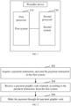
- FIG. 1 is a diagram illustrating an application environment to which a payment method according to an embodiment is applied.
- the application environment includes a wearable device, and the wearable device includes a first processor 110 and a second processor 120.
- the first processor 110 and the second processor 120 are both microprocessors.
- the first processor 110 may be used as a main processor, and the second processor 120 may be used as a coprocessor.
- Each of the first processor 110 and the second processor 120 may be configured as a corresponding microprocessor according to actual applications; for example, the first processor 110 is configured as a Qualcomm processor, and the second processor 120 is configured as an MCU processor, which is not limited herein.
- the first processor 110 is integrated with an operating system different from the second processor 120.
- the first processor is configured to run a first system
- the second processor is configured to run a second system
- power consumption of the first system integrated into the first processor 110 is higher than power consumption of the second system integrated into the second processor 120.
- the first processor 110 may be a Central Processing Unit (CPU) processor
- the corresponding first system may be an Android (Android) system.
- the second processor 120 may be a Microcontroller Unit (MCU) processor
- the corresponding second system may be a Real Time Operating System (RTOS). That is, the wearable device is a dual-core and dual-system electronic device.
- MCU Microcontroller Unit
- RTOS Real Time Operating System
- the wearable device may be, but is not limited to, a smart watch, a smart bracelet, or the like.
- the wearable device may include multiple operating states.
- a first system state means that the first processor controls running of the wearable device and is responsible for logical operations of data, whereas the second processor plays an auxiliary role, and is configured to collect data, such as state data of the user, for provision to the first processor.
- the first system state it may mainly make the first system operate, and the second system is in a sleep state for most of the time; alternatively, the first system and the second system may operate at the same time, for example, the Android system and the RTOS system operate at the same time, which ensures not only basic functions of the wearable device, but also extended functions of the wearable device, being fully functional.
- a second system state means that the wearable device mainly or only runs the second system, and the running of the wearable device is controlled by the second processor; for example, the Android system is closed, and only the RTOS system is run, which may enable low power consumption and an ultra-long standby time.
- the main frequency of the CPU may be up to 1.2 GHz (gigahertz), and the main frequency of the MCU is about 320MHz (megahertz).
- the power consumption of the first processor is higher than the power consumption of the second processor, and the power consumption of the first system is higher than the power consumption of the second system.
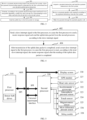
- FIG. 2 is a flowchart of a payment method according to an embodiment.
- the payment method in the embodiment is executed in the second system state, and it is controlled by the second processor.
- the method includes operations as follows.
- Operation 202 a payment instruction is acquired, and the payment instruction sent to the first system.
- the wearable device is currently in the second system state, in which state the second processor controls data processing of the wearable device.
- the wearable device may automatically switch, according to a current operating state, from the first system state to the second system state. For example, upon detecting that the current power of the wearable device is lower than a preset threshold, it automatically switches to the second system state.
- a user's operation may also be received, and the wearable device is controlled, according to the user's operation, to operate in the second system state.
- the wearable device implements various functions through a low-performance system, and the power of the wearable device can be saved, which prolongs the standby time.
- the payment instruction is used to instruct the first system to generate a corresponding payment graphic code.
- the payment instruction may carry a timestamp, and according to the timestamp, the first system generates the payment graphic code that dynamically changes over time.
- Algorithms and forms of generating the payment graphic code are not limited, including but not limited to stacked two-dimensional bar code, or row type two-dimensional bar code, or two-dimensional matrix bar code, or the like.
- the user's operation is monitored by the second system, and the payment instruction is generated according to a payment operation when the payment operation is monitored, where the payment instruction is an instruction generated when there is a need to make the payment with the graphic code.
- the wearable device is an electronic watch, and the payment instruction is generated through an operation performed by the user on a payment interface currently displayed by the electronic watch.
- the payment operation includes, but is not limited to, a touch operation, a gesture operation, a voice operation, and the like.
- Operation 204 a payment graphic code returned, according to the payment instruction, from the first system is received.
- the payment graphic code is a graphic code carrying payment information, and it may be in the form of a two-dimensional code or in other forms, where the payment information includes, but is not limited to, a payment account identifier, payment user's identity information, timestamp information, payment running number, and the like.
- the second system needs to send the payment instruction to the first system, so that the payment graphic code is generated by the first system.
- Communication between the first system and the second system may perform data exchange through communication between the first processor and the second processor.
- the first processor and the second processor may communicate with each other through a predefined protocol.
- dual-core communication channels perform reliable data transmission between the Qualcomm chip and the MCU chip through a Serial Peripheral Interface (SPI) protocol.
- SPI Serial Peripheral Interface
- the payment graphic code returned, according to the payment instruction, from the first system may be an unencrypted payment graphic code, or may be an encrypted payment graphic code generated after encryption.
- the first system and the second system may predetermine an encryption algorithm, so that the second system, upon receiving the encrypted payment graphic code, performs correct decryption to obtain the decrypted payment graphic code.
- the encryption algorithm includes, but is not limited to, a symmetric encryption algorithm, an asymmetric encryption algorithm, and the like.
- an RSA encryption algorithm is used to ensure that the encrypted two-dimensional code data is not stolen, and ensure the security use of the two-dimensional code in the second system state.
- the RSA encryption algorithm is an asymmetric encryption algorithm through which decryption may be performed without directly transferring the key, this ensures the security of the information and avoids the risk of cracking that would be caused when the key is directly transferred.
- a pair of keys referred to as a public key and a private key respectively, are used to perform the encryption and decryption processes, where the private key is stored by one party for decryption, and the public key is sent to another party for encrypting the information.
- the second system parses the payment graphic code, renders and displays the graphic code on the corresponding payment interface, and information in the payment graphic code is acquired through scanning of a code scanning device, thereby making the payment.
- the payment graphic code is transmitted to a payment application, and the payment application renders the payment graphic code with a parsing and rendering module, and displays the payment graphic code on a graphic code presentation interface of the payment application.
- the subsequent display and payment process may be done by the second system, and the payment function can also be enabled under the low-performance system.
- the payment method is applied to a wearable device, where the wearable device includes a first processor and a second processor.
- the first processor is configured to run a first system
- the second processor is configured to run a second system.
- the wearable device is in a second system state, and the power consumption of the second processor is lower than the power consumption of the first processor.
- a payment instruction is acquired, and the payment instruction is sent to the first system.
- a payment graphic code returned, according to the payment instruction, from the first system is received, and the payment is made through the payment graphic code.
- the whole payment process is done in the second system state, and it is controlled by a low power consumption processor.
- the payment graphic code is received through dual-core communication and is displayed, the payment is done through the low-performance system. In this way, the payment function, which otherwise cannot be realized on the low-performance system, is enabled by means of the high-performance of the second system.
- the payment instruction is configured to wake up the first system, and instruct the first system to generate the payment graphic code according to the payment instruction. And after operation 204, the method further includes: returning response information to the first system, where the response information is used to instruct the first system to enter a sleep state.
- the first system is woken up through the payment instruction. After the payment graphic code returned from the first system is received, the first system is instructed to enter the sleep state by returning the response information to the first system.
- the subsequent display and payment process may be done through the second system, and the first system is in the sleep state; as such, the power consumption of the wearable device is reduced, the payment function can be enabled in a low power state, since the first system is controlled to be in the sleep state for most of the time in the whole payment process.
- the first system is woken up only when the payment graphic code needs to be generated, and the first system enters the sleep state after the payment graphic code is received, thereby further reducing the power consumption of the first system, enabling the payment under a low power consumption condition, and improving resource utilization.
- the returning the response information to the first system includes: performing verification on the payment graphic code, and generating the response information upon determining that the verification is passed.
- the payment graphic code may include current verification information, and standard verification information is prestored in the second system.
- the first system extracts the current verification information from the received payment graphic code, and if no current verification information is extracted, or the extracted current verification information does not match the standard verification information, it indicates that the verification on the payment graphic code fails, or that the payment graphic code may be damaged and a new payment graphic code needs to be requested again from the first system. If the verification is passed, the response information is generated, where the response information is used to notify the first system that a valid payment graphic code has been received, so as to switch the first system to the sleep state, thereby reducing the power consumption.
- a re-transmission notification may be returned to the first system, to cause the first system to regenerate a payment graphic code and return it to the second system. If the payment graphic code is damaged during transmission or the generated payment graphic code is incorrect, the invalid payment graphic code may be detected in the verification, so that the re-transmission notification is returned to the first system device.
- the re-transmission notification may carry a current time, so that the first system regenerates an updated payment graphic code according to the current time.
- the validity of the payment graphic code is improved, and payment failure is avoided. Only when the verification is passed, the response information is generated, which further ensures the reliability of the payment graphic code.
- the method further includes operations as follows.
- a payment preprocessing request is sent from the first system, where the payment preprocessing request is generated by the first system based on a user payment authorization instruction.
- the user payment authorization instruction is generated when the user allows a graphic code to be used to make a payment on the wearable device, and it may be generated in the first system state through an operation performed on an authorization setting interface of the wearable device. In the first system state, it may mainly make the first system operate, an authorization setting operation is received through the first system, and the user payment authorization instruction is generated. In an embodiment, the user payment authorization instruction is generated through an operation performed on a user payment authorization key in a pop-up box displayed on an interface of the wearable device.
- the first processor After the first system acquires the user payment authorization instruction, it indicates that the user allows to pay through the graphic code, the first processor generates the payment preprocessing request and sends it to the second processor.
- the payment preprocessing request is used to instruct the second processor to generate, based on an encryption algorithm, a public key and a private key corresponding to each other, to ensure secure transmission of the payment graphic code, and ensure payment validity.
- Operation 304 a public key and a private key corresponding to each other are generated based on an encryption algorithm according to the payment preprocessing request, and the private key is stored in the second system.
- the second system needs to generate the public key and private key corresponding to each other in advance based on an encryption algorithm.
- the public key is stored in the first system, for the first system to encrypt the generated payment graphic code with the public key.
- the private key is stored in the second system, for the second system to decrypt the encrypted payment graphic code received.
- the algorithm for generating the public key and private key corresponding to each other may be customized.
- the public key and the private key are generated through the RSA asymmetric encryption algorithm, where the RSA asymmetric encryption algorithm adopts coprime numbers as large as possible to ensure the high reliability of encryption.
- the second system sends, through a dual-core communication protocol, the public key to the first system for storage.
- Channel security is enabled for the delivery of the generated public key by means of the reliable dual-core communication, so that the overall reliability of the payment graphic code can be achieved.
- the first system instructs the second system to generate a public key and a private key based on an encryption algorithm, and send the public key to the first system through dual-core communication.
- the first system stores the public key after receiving it, and waits for a graphic code payment instruction sent from the first system.
- the security of subsequent transmission of the payment graphic code is ensured by generating the public key and the private key in advance, which improves the reliability of payment.
- operation 204 includes: receiving an encrypted payment graphic code that is encrypted by the first system with the public key; and decrypting the encrypted payment graphic code with the private key, to obtain the payment graphic code.
- the second system decrypts the encrypted payment graphic code by using the private key, to obtain the decrypted payment graphic code. Only the private key can enable the decryption to be successful, so that the payment graphic code can be used, thereby improving the transmission security of the payment graphic code.
- the public key is transmitted to the first system from the second system, and the encrypted payment graphic code is transmitted to the second system from the first system.
- the encrypted payment graphic code and the public key are intercepted by a hacker, there is no danger, because only the private key of the second system can decrypt the message, thereby preventing leakage of contents of the message.
- operation 206 includes: transferring the payment graphic code to a user interface, and displaying the payment graphic code on the user interface.
- the second system sends the payment graphic code to a UI user interface for parsing and display, so that the payment may be done through graphic code in a low power consumption mode.
- a display screen of the wearable device is connected to the first processor and the second processor through a Mobile Industry Processor Interface (MIPI), and may display the data output by the first processor or the second processor.
- MIPI Mobile Industry Processor Interface
- the data analysis and display of the graphic code are performed by the low-power processor, i.e., the second processor, which reduces the power consumption of the wearable device.
- the payment graphic code in the second system state, may be displayed through the low-performance system, which ensures the use of the payment function of the wearable device under the low-performance system, and reduces the power consumption of the wearable device.
- the method further includes: detecting an operating state of the wearable device; and upon determining that the operating state meets a low power consumption condition, switching the wearable device to operate in the second system state, and controlling the first system to enter the sleep state.
- the operating state of the wearable device includes a device state of the wearable device itself, and may further include a user state collected by the wearable device.
- the device state includes a state of charge, a device temperature state, a device motion state, and the like.
- the state of charge includes a low power state and a high power state.
- the device temperature state includes a normal temperature state and an abnormal temperature state.
- the device motion state includes a device motion speed, a device rotation angle, and the like.
- the user state includes at least one of a heart rate, attention information (such as eyeball position information), and cardiopulmonary data of the user, but is not limited thereto.
- the low power consumption condition may be customized; for example, the low power state, the abnormal temperature state, a state where the motion speed of the device is greater than a preset threshold, a state where the heart rate is lower than a preset threshold, and the like, may all be considered as meeting the low power consumption condition.
- a state vector is defined by various states in the device state and the user state, and it is determined, based on the state vector, whether the low power consumption condition is met. For example, a standard state vector corresponding to the low power consumption condition is preset, and matching is performed between the current state vector defined by various states of the wearable device and the standard state vector; and if the matching is successful, it is considered that the low power consumption condition is met. It may be flexibly determined, according to settings for various states of the wearable device, whether the wearable device meets the low power consumption condition or not, so that the wearable device is accordingly switched to operate in the second system state, and the first system is controlled to enter the sleep state, which reduces the power consumption.
- the operating state of the wearable device is automatically detected; and upon determining that the operating state meets the low power consumption condition, the wearable device is automatically switched to operate in the second system state, and the first system is controlled to enter the sleep state, thereby reducing the power consumption.
- an uplink data packet is transmitted from the second processor to the first processor.
- the second processor transmitting the uplink data packet to the first processor includes operations as follows.
- a slave interrupt signal is sent to the first processor, to cause the first processor to send a master response signal and read the uplink data packet from the second processor, according to the slave interrupt signal.
- the uplink data packet may include at least one of an operation instruction and service data that are received or generated by the second processor.
- the uplink data packet may be the payment instruction acquired by the second system, the response information generated after receipt of the payment graphic code, the public key generated based on the encryption algorithm, and the like.
- the slave interrupt signal is used to force an interruption and indicate that there are some uplink data needed to be transmitted from the first processor to the first processor. Specifically, upon detecting that there is an uplink data packet, the second processor of the electronic device may generate a corresponding slave interrupt signal according to the uplink data packet, and send the generated slave interrupt signal to the first processor through a slave interrupt interface after locking a data transmission interface.
- the first processor may read the uplink data packet from the second processor, and send the master response signal to the second processor.
- the master response signal is used to indicate that the first processor is in a data transmission state.
- a reset slave interrupt signal is sent to the first processor, to cause the first processor to reset, according to the reset slave interrupt signal, the master response signal after the reading of the uplink data packet is completed.
- the second processor may reset the slave interrupt signal, after the transmission of the uplink data packet is completed.
- the first processor may receive the reset slave interrupt signal.
- the reset slave interrupt signal may indicate that the second processor has completed the transmission of data.
- the first processor may reset the master response signal when obtaining the reset slave interrupt signal.
- the first processor may read the data packet upon receiving the slave interrupt signal; and after the reading of data is completed, the first processor may reset the master response signal according to the reset slave interrupt signal that is reset by the second processor, where the reset master response signal indicates that single data transmission has been completed. This reduces the delay of communication between the processors, and improves the communication efficiency of the processors.
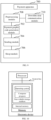
- the wearable device includes a first processor 310 corresponding to the first system and a second processor 320 corresponding to the second system.
- the wearable device may include one or more of a heart rate sensor 321, an accelerometer + gyroscope 322, an atmospheric pressure sensor 323, a touch sensor 324, a magnetometer sensor 325, and a micro differential pressure sensor 326.
- the second processor 320 may be connected to the sensor(s) included in the wearable device, and configured to acquire data collected by the sensor(s).
- the second processor 320 may be further connected to a Global Positioning System (GPS) module 327, and be configured to acquire positioning data received by a GPS antenna.
- the second processor 320 may be further connected to a debug (DEBUG) module 328, and be configured to output debugging data of the wearable device.
- the first processor 310 and the second processor 320 are connected through a Serial Peripheral Interface (SPI), so that the first system and the second system may transmit communication data through the SPI bus.
- the display screen 330 is connected to the first processor 310 and the second processor 320 through a Mobile Industry Processor Interface (MIPI), and may display data output by the first processor 310 or the second processor 320.
- the first processor 310 further includes a sensor hub driver which may be configured to drive data collection and processing of various sensors.
- the first processor 310 is a Qualcomm chip on which the Android system is run
- the second processor 320 is an MCU chip on which the RTOS system is run
- the payment method includes operations as follow.
- the Android system receives a two-dimensional code payment authorization operation performed on an interface, determines that the user has a payment requirement, and generates a payment preprocessing request.
- the Android system sends the payment preprocessing request to the MCU.
- the MCU generates a public key and a private key by using the RSA encryption algorithm, sends the public key to the Android system through a dual-core communication SPI protocol, and stores the private key locally for decrypting the two-dimensional code and displaying it.
- the Android system stores the public key after receiving it, and waits for the MCU to send a two-dimensional code payment instruction.
- the MCU monitors a payment action of the user in a low power consumption state, and sends the payment instruction to the Android system to wake up the Android system, upon monitoring a two-dimensional code payment request.
- the Android system Upon receiving the payment instruction, the Android system is waked up to generate a two-dimensional code, and encrypt the generated two-dimensional code with the prestored public key.
- the Android system transmits the encrypted two-dimensional code to the MCU through the dual-core communication SPI protocol.
- the MCU After receiving data responsive to the payment instruction, the MCU obtains two-dimensional code data through decryption with the private key of the MCU itself, and returns, to the Android system, response information to instruct the Android system to enter the sleep state.
- the MCU sends the two-dimensional code data to the UI for parsing and display, and two-dimensional code payment is made in the low-performance system.
- dual-core communication channels perform reliable data transmission between the Qualcomm chip and the MCU chip through the SPI protocol, and the RSA encryption algorithm is used to protect the encrypted two-dimensional code data from been stolen. This ensures the security use of the two-dimensional code in the low power consumption mode under the low-performance system.
- the MCU receives the two-dimensional code data sent by the Android system, and makes the two-dimensional code payment safely and reliably in the low power consumption condition.
- a payment method is provided.
- the payment method is applied to a wearable device, where the wearable device includes a first processor and a second processor.
- the first processor is configured to run a first system
- the second processor is configured to run a second system.
- the wearable device is in a second system state, and power consumption of the second processor is lower than power consumption of the first processor.
- the method includes operations as follows.
- Operation 502 a payment instruction sent from the second system is received, and a corresponding payment graphic code is generated according to the payment instruction.
- the payment graphic code is sent to the second system, where the payment graphic code is used for the second system to make a payment.
- the wearable device includes a first processor and a second processor, where the first processor is configured to run a first system, and the second processor is configured to run a second system.
- the wearable device is in a second system state, and the power consumption of the second processor is lower than the power consumption of the first processor.
- a payment instruction sent from the second system is received, and a corresponding payment graphic code is generated according to the payment instruction.
- the payment graphic code is sent to the second system, where the payment graphic code is used for the second system to make a payment.
- the whole payment process is done in the second system state, and it is controlled by the low power consumption processor.
- the payment graphic code is received through the dual-core communication and is displayed, and the payment is made through the low-performance system. In this way, the payment function, which otherwise cannot be realized on the low-performance system, is enabled by means of the high-performance of the second system.
- operation 502 includes: entering a working state according to the payment instruction. And after operation 504, the method further includes: receiving response information returned by the second system, and entering the sleep state according to the response information.
- the method further includes: acquiring a user payment authorization instruction, when being in the working state; sending a payment preprocessing request to the second system according to the user payment authorization instruction, where the payment preprocessing request is used to instruct the second system to generate, based on an encryption algorithm, a public key and a private key corresponding to each other, and store the private key in the second system; and receiving the public key returned from the second system, and storing the public key.
- operation 502 includes: generating an encrypted payment graphic code which is encrypted with public key.
- Operation 504 includes: sending the encrypted payment graphic code to the second system.
- a downlink data packet is transmitted from the first processor to the second processor.
- the first processor transmitting the downlink data packet to the second processor includes: in response to detecting a downlink data packet, sending, by the first processor, a master interrupt signal to the second processor; receiving, by the first processor, a slave response signal returned, according to the master interrupt signal, from the second processor; sending, by the first processor, the downlink data packet to the second processor according to the slave response signal, and resetting the master interrupt signal after the sending is completed.
- the reset master interrupt signal is used to instruct the second processor to reset the slave response signal after processing of the downlink data packet is completed.
- the downlink data packet may include at least one of an operation instruction and service data that are received or generated by the first processor; for example, it may be a payment graphic code.
- the operation instruction may be used to instruct, after being transmitted to the second processor, the second processor to perform a corresponding service operation.
- the service data is used to provide, after being transmitted to the second processor, data support for the second processor to perform a service operation corresponding to the service data.
- the master interrupt signal is used to force an interruption and indicate that there is a downlink data packet needed to be transmitted from the second processor to the second processor. Specifically, upon detecting that there is a downlink data packet, the first processor of the electronic device may generate a corresponding master interrupt signal according to the downlink data packet, and send the generated master interrupt signal to the second processor through a master interrupt interface.
- the slave response signal is used to indicate that the second processor is ready to receive the downlink data packet. Data transmission between the first processor and the second processor needs to be implemented through a data transmission interface.
- the reset master interrupt signal may indicate that the first processor has completed the transmission of data.
- the first processor may reset the master interrupt signal to notify the second processor that the transmission of the downlink data packet has been completed.
- the second processor receives the downlink data packet, and may process the downlink data packet.
- the second processor may reset the slave response signal, after the reset master interrupt signal is received and the processing of the downlink data packet is completed.
- the second processor may set a slave response interface to be a low level state.
- the reset slave response signal is used to notify the first processor that the second processor has completed the processing of the downlink data packet.
- the first processor may send the master interrupt signal again to the second processor to perform data transmission.
- the first processor may send a master interrupt signal to the second processor, and receive a slave response signal returned, according to the master interrupt signal, from the second processor.
- the first processor may send the downlink data packet to the second processor according to the slave response signal, and reset the master interrupt signal after the sending is completed.
- the reset master interrupt signal may instruct the second processor to reset the slave response signal after completing the processing of the downlink data packet. That is, the data packet may be transmitted upon receipt of the slave response signal, and the master interrupt signal is reset after the transmission is completed, where the reset master interrupt signal indicates that single data transmission has been completed. In this way, there is no need to introduce the slave interrupt signal and the master response signal for secondary confirmation, the delay of communication between the processors can be reduced, and the communication efficiency of the processors is improved.
- 7 may include multiple sub-operations or multiple phases, and these sub-operations or phases are not necessarily performed at the same moment, instead they may be performed at different moments; and these sub-operations or phases are not necessarily performed sequentially, instead they may be performed in turn or alternately with other operations or with at least part of the sub-operations or phases of other operations.
- FIG. 8 is a structural block diagram illustrating a payment apparatus according to an embodiment.
- a payment apparatus 600 is provided, which is applied to a wearable device.
- the wearable device includes a first processor and a second processor, the first processor is configured to run a first system, and the second processor is configured to run a second system.
- the wearable device is in a second system state, and power consumption of the second processor is lower than power consumption of the first processor.
- the apparatus includes a payment instruction sending module 602, a payment graphic code receiving module 604, a response module 606, and a payment module 608.
- the payment instruction sending module 602 is configured to acquire a payment instruction, and send the payment instruction to the first system.
- the payment graphic code receiving module 604 is configured to receive a payment graphic code returned, according to the payment instruction, from the first system.
- the payment module 606 is configured to make a payment through the payment graphic code.
- the foregoing payment apparatus makes the payment through the payment graphic code.
- the whole payment process is done in the second system state, and it is controlled by a low power consumption processor.
- the payment graphic code is received through dual-core communication and is displayed, and the payment is done through the low-performance system. In this way, the payment function, which otherwise cannot be realized on the low-performance system, is enabled by means of the high-performance of the second system.
- the payment instruction is configured to wake up the first system, to instruct the first system to generate, according to the payment instruction, a payment graphic code.
- the apparatus further includes the response module 608.
- the response module 608 is configured to return response information to the first system, where the response information is used to instruct the first system to enter a sleep state.
- the first system is woken up only when the payment graphic code needs to be generated, and the first system enters the sleep state after the payment graphic code is received.
- the power consumption of the first system is further reduced, and the payment is made under a lower power consumption condition, which improves the resource utilization.
- the response module 608 is further configured to perform verification on the payment graphic code, and generate the response information when the verification is passed.
- the validity of the payment graphic code is improved, and payment failure is avoided. Only when the verification is passed, the response information is generated, which further ensures the reliability of the payment graphic code.
- the apparatus further includes: a preprocessing module 610, configured to: receive a payment preprocessing request sent from the first system, where the payment preprocessing request is generated by the first system based on a user payment authorization instruction; according to the payment preprocessing request, generate, based on an encryption algorithm, a public key and a private key corresponding to each other; and store the private key in the second system, and send the public key to the first system for storage.
- a preprocessing module 610 configured to: receive a payment preprocessing request sent from the first system, where the payment preprocessing request is generated by the first system based on a user payment authorization instruction; according to the payment preprocessing request, generate, based on an encryption algorithm, a public key and a private key corresponding to each other; and store the private key in the second system, and send the public key to the first system for storage.
- the first system instructs the second system to generate a public key and a private key based on an encryption algorithm, and send the public key to the first system through dual-core communication.
- the first system stores the public key after receiving it, and waits for a graphic code payment instruction sent from the first system.
- the security of subsequent transmission of the payment graphic code is ensured by generating the public key and the private key in advance, which improves the reliability of payment.
- the payment graphic code receiving module 604 is further configured to receive an encrypted payment graphic code that is encrypted by the first system - with the public key; and decrypt the encrypted payment graphic code with the private key, to obtain the payment graphic code.
- the public key is transmitted to the first system from the second system, and the encrypted payment graphic code is transmitted to the second system from the first system.
- the encrypted payment graphic code and the public key are intercepted by a hacker, there is no danger, because only the private key of the second system can decrypt the message, thereby preventing leakage of contents of the message.
- the payment module 606 is further configured to transfer the payment graphic code to a user interface, and display the payment graphic code on the user interface.
- the payment graphic code in the second system state, may be displayed through the low-performance system, which ensures the use of the payment function of the wearable device under the low-performance system, and reduces the power consumption of the wearable device.
- the apparatus further includes: a mode switching module 612, configured to detect an operating state of the wearable device; and when the operating state meets a low power consumption condition, switch the wearable device to operate in the second system state, and control the first system to enter the sleep state.
- a mode switching module 612 configured to detect an operating state of the wearable device; and when the operating state meets a low power consumption condition, switch the wearable device to operate in the second system state, and control the first system to enter the sleep state.
- the operating state of the wearable device is automatically detected; and upon determining that the operating state meets the low power consumption condition, the wearable device is automatically switched to operate in the second system state, and the first system is controlled to enter the sleep state, thereby reducing the power consumption.
- an uplink data packet is transmitted from the second processor to the first processor
- the apparatus further includes: an uplink data communication module 614, configured to: send a slave interrupt signal to the first processor, to cause the first processor to send a master response signal and read the uplink data packet from the second processor, according to the slave interrupt signal; and after transmission of the uplink data packet is completed, send a reset slave interrupt signal to the first processor, to cause the first processor to reset, according to the reset slave interrupt signal, the master response signal after the reading of the uplink data packet is completed.
- the first processor may read the data packet upon receiving the slave interrupt signal; and after the reading of data is completed, the first processor may reset the master response signal according to the reset slave interrupt signal that is reset by the second processor, where the reset master response signal indicates that single data transmission has been completed. This reduces the delay of communication between the processors, and improves the communication efficiency of the processors.
- FIG. 9 is a structural block diagram of a payment apparatus of an embodiment.
- a payment apparatus 700 is provided, which is applied to a wearable device.
- the wearable device includes a first processor and a second processor, the first processor is configured to run a first system, and the second processor is configured to run a second system.
- the wearable device is in a second system state, and power consumption of the second processor is lower than power consumption of the first processor.
- the apparatus includes a payment graphic code generation module 702 and a sending module 704.
- the payment graphic code generation module 702 is configured to receive a payment instruction sent from the second system, and generate a corresponding payment graphic code according to the payment instruction.
- the sending module 704 is configured to send the payment graphic code to the second system, where the payment graphic code is used for the second system to make a payment.
- the whole payment process is done in the second system state, and it is controlled by the low power consumption processor.
- the payment graphic code is received through the dual-core communication and is displayed, and the payment is made through the low-performance system. In this way, the payment function, which otherwise cannot be realized on the low-performance system, is enabled by means of the high-performance of the second system.
- the payment graphic code generation module 702 is further configured to make a working state entered according to the payment instruction.
- the apparatus further includes a sleep module 706, configured to receive response information returned from the second system, and make the sleep state entered according to the response information.
- the first system is woken up only when the payment graphic code needs to be generated, and the first system enters the sleep state after the payment graphic code is received.
- the power consumption of the first system is further reduced, and the payment is made under a lower power consumption condition, which improves the resource utilization.
- the apparatus further includes: a preprocessing module 708, configured to: acquire a user payment authorization instruction when being in the working state; send a payment preprocessing request to the second system according to the user payment authorization instruction, where the payment preprocessing request is used to instruct the second system to generate, based on an encryption algorithm, a public key and a private key corresponding to each other and store the private key in the second system; and receive the public key returned from the second system, and store the public key.
- a preprocessing module 708 configured to: acquire a user payment authorization instruction when being in the working state; send a payment preprocessing request to the second system according to the user payment authorization instruction, where the payment preprocessing request is used to instruct the second system to generate, based on an encryption algorithm, a public key and a private key corresponding to each other and store the private key in the second system; and receive the public key returned from the second system, and store the public key.
- the first system instructs the second system to generate a public key and a private key based on an encryption algorithm, and send the public key to the first system through dual-core communication.
- the first system stores the public key after receiving it, and waits for a graphic code payment instruction sent from the first system.
- the security of subsequent transmission of the payment graphic code is ensured by generating the public key and the private key in advance, which improves the reliability of payment.
- the payment graphic code generation module 702 is further configured to generate an encrypted payment graphic code which is encrypted based on the public key.
- the sending module 704 is further configured to send the encrypted payment graphic code to the second system.
- the public key is transmitted to the first system from the second system, and the encrypted payment graphic code is transmitted to the second system from the first system.
- the encrypted payment graphic code and the public key are intercepted by a hacker, there is no danger, because only the private key of the second system can decrypt the message, thereby preventing leakage of contents of the message.
- a downlink data packet is transmitted from the first processor to the second processor
- the apparatus further includes: a downlink data communication module 710, configured to: send, by the first processor, a master interrupt signal to the second processor when a downlink data packet is detected; receive, by the first processor, a slave response signal that is returned from the second processor according to the master interrupt signal; send, by the first processor, the downlink data packet to the second processor according to the slave response signal; and reset the master interrupt signal after the sending is completed.
- the reset master interrupt signal is used to instruct the second processor to reset the slave response signal after processing of the downlink data packet is completed.
- the first processor may send a master interrupt signal to the second processor, and receive a slave response signal returned, according to the master interrupt signal, from the second processor.
- the first processor may send the downlink data packet to the second processor according to the slave response signal, and reset the master interrupt signal after the sending is completed.
- the reset master interrupt signal may instruct the second processor to reset the slave response signal after completing the processing of the downlink data packet. That is, the data packet may be transmitted upon receipt of the slave response signal, and the master interrupt signal is reset after the transmission is completed, where the reset master interrupt signal indicates that single data transmission has been completed. In this way, there is no need to introduce the slave interrupt signal and the master response signal for secondary confirmation, the delay of communication between the processors can be reduced, and the communication efficiency of the processors is improved.
- the payment apparatus may be divided into different modules as required, to implement all or part of the functions of the payment apparatus mentioned above.
- the various modules in the payment apparatus mentioned above may be implemented completely or partly in software, hardware, and a combination thereof.
- the foregoing modules may be in a hardware form, and embedded in or independent of a processor in a computer device; or they may be in a form of software and stored in a memory in the computer device, so that the processor invokes and executes the operations corresponding to the foregoing modules.
- FIG. 10 is a schematic diagram illustrating an internal structure of an electronic device according to an embodiment.
- the electronic device includes a processor and a memory connected by a system bus.
- the processor is configured to provide calculation and control capabilities to support operations of the entire electronic device.
- the memory may include a non-volatile storage medium and an internal memory.
- the non-volatile storage medium stores an operating system and a computer program.
- the computer program may be executed by the processor to implement the payment method provided in the following embodiments.
- the internal memory provides a cached operating environment for the operating system and the computer program in the non-volatile storage medium.
- the electronic device may be various wearable devices.
- the various modules in the payment apparatuses provided in the embodiments of the present disclosure may be implemented in the form of a computer program.
- the computer program may run on a terminal or a server.
- Program modules defined by the computer program may be stored in a memory of the electronic device.
- the computer program is executed by a processor, operations of the method described in the embodiments of the present disclosure are implemented.
- the embodiments of the present disclosure further provide a computer-readable storage medium.
- One or more non-transitory computer-readable storage media contain computer-executable instructions, and when being executed by one or more processors, the computer-executable instructions cause the processor(s) to perform operations of the payment methods.
- a computer program product including instructions which, when being executed on a computer, cause the computer to perform the payment methods.
- the memory, storage, database, or any other referred media as used herein may include a non-volatile and/or volatile memory.
- the non-volatile memory may include a read-only memory (ROM), a programmable ROM (PROM), an electrically programmable ROM (EPROM), an electrically erasable programmable ROM (EEPROM), or a flash memory.
- the volatile memory may include a random access memory (RAM), which functions as an external cache memory.
- the RAM is available in many forms, such as static RAM (SRAM), dynamic RAM (DRAM), synchronous DRAM (SDRAM), double data rate SDRAM (DDR SDRAM), enhanced SDRAM (ESDRAM), Synch link (Synch link) DRAM (SLDRAM), Rambus direct RAM (RDRAM), direct Rambus dynamic RAM (DRDRAM), and Rambus dynamic RAM (RDRAM).
- SRAM static RAM
- DRAM dynamic RAM
- SDRAM synchronous DRAM
- DDR SDRAM double data rate SDRAM
- ESDRAM enhanced SDRAM
- SLDRAM Synch link (Synch link) DRAM
- RDRAM Rambus direct RAM
- DRAM direct Rambus dynamic RAM
- RDRAM Rambus dynamic RAM
Landscapes
- Business, Economics & Management (AREA)
- Engineering & Computer Science (AREA)
- Accounting & Taxation (AREA)
- Strategic Management (AREA)
- Physics & Mathematics (AREA)
- General Business, Economics & Management (AREA)
- General Physics & Mathematics (AREA)
- Theoretical Computer Science (AREA)
- Computer Networks & Wireless Communication (AREA)
- Computer Security & Cryptography (AREA)
- Finance (AREA)
- Power Sources (AREA)
Abstract
Description
- This application claims priority to
Chinese Patent Application No. 202011630586.1 entitled "Payment Method and Apparatus, Electronic Device and Computer-Readable Medium" and filed before China National Intellectual Property Administration on December 30, 2020 - The present disclosure relates to the field of communications technologies, and in particular to a payment method and apparatus, an electronic device, and a computer-readable storage medium.
- Smart wearable devices are becoming more and more popular, especially smart watches and bracelets have been favored by more and more young people. The smart wearable device has not only functions of a traditional watch such as a clock function, but also some functions of other electronic devices, such as a payment function.
- However, in a traditional method for payment with a smart wearable device, the payment can be made only through a high-performance system, and is unable to be made under a low-performance system.
- Embodiments of the present disclosure provide a payment method and apparatus, an electronic device and a computer-readable storage medium.
- A payment method is provided, which is applied to a wearable device. The wearable device includes a first processor and a second processor. The first processor is configured to run a first system, and the second processor is configured to run a second system. The wearable device is in a second system state, and power consumption of the second processor is lower than power consumption of the first processor. The method includes:
- acquiring a payment instruction, and sending the payment instruction to the first system;
- receiving a payment graphic code returned, according to the payment instruction, from the first system; and
- making a payment through the payment graphic code.
- A payment apparatus is provided, which is applied to a wearable device. The wearable device includes a first processor and a second processor. The first processor is configured to run a first system, and the second processor is configured to run a second system. The wearable device is in a second system state, and power consumption of the second processor is lower than power consumption of the first processor. The apparatus includes:
- a payment instruction sending module, configured to acquire a payment instruction, and send the payment instruction to the first system;
- a payment graphic code receiving module, configured to receive a payment graphic code returned, according to the payment instruction, from the first system; and
- a payment module, configured to make a payment through the payment graphic code.
- An electronic device is provided, which includes a memory and a processor. The memory stores therein a computer program which, when being executed by the processor, causes the processor to perform operations of the method mentioned above.
- A computer-readable storage medium is provided, which has a computer program stored thereon. The computer program, when being executed by a processor, causes operations of the method mentioned above to be implemented.
- In the payment method and apparatus, the electronic device and the computer-readable storage medium mentioned above, they are applied to wearable device, and the wearable device includes a first processor and a second processor. The first processor is configured to run a first system, and the second processor is configured to run a second system. The wearable device is in a second system state, and the power consumption of the second processor is lower than power consumption of the first processor. A payment instruction is acquired, and the payment instruction is sent to the first system. A payment graphic code returned, according to the payment instruction, from the first system is received. A payment is made through the payment graphic code. The whole payment process is done in the second system state, and it is controlled by a low power consumption processor. The payment graphic code is received through dual-core communication and is displayed, and the payment is done through the low-performance system. In this way, the payment function, which otherwise cannot be realized on the low-performance system, is enabled by means of the high-performance of the second system.
- A payment method is provided, which is applied to a wearable device. The wearable device includes a first processor and a second processor, the first processor is configured to run a first system, and the second processor is configured to run a second system. The wearable device is in a second system state, and power consumption of the second processor is lower than power consumption of the first processor. The method includes:
- receiving a payment instruction sent from the second system, and generating a corresponding payment graphic code according to the payment instruction; and
- sending the payment graphic code to the second system, where the payment graphic code is configured to make a payment through the second system.
- A payment apparatus is provided, which is applied to a wearable device. The wearable device includes a first processor and a second processor, the first processor is configured to run a first system, and the second processor is configured to run a second system. The wearable device is in a second system state, and power consumption of the second processor is lower than power consumption of the first processor. The apparatus includes:
- a payment graphic code generation module, configured to receive a payment instruction sent from the second system, and generate a corresponding payment graphic code according to the payment instruction; and
- a sending module, configured to send the payment graphic code to the second system, where the payment graphic code is configured to make a payment through the second system.
- An electronic device is provided, which includes a memory and a processor. The memory stores a computer program which, when being executed by the processor, causes the processor to perform operations of the method mentioned above.
- A computer-readable storage medium is provided, which has a computer program stored thereon. The computer program, when being executed by a processor, causes operations of the method mentioned above to be implemented.
- In the above payment method and apparatus, the electronic device and the computer-readable storage medium, they are applied to a wearable device, and the wearable device includes a first processor and a second processor. The first processor is configured to run a first system, and the second processor is configured to run a second system. The wearable device is in a second system state, and the power consumption of the second processor is lower than the power consumption of the first processor. The payment instruction sent from the second system is received, and a corresponding payment graphic code is generated according to the payment instruction. The payment graphic code is sent to the second system, for the second system to make a payment. The whole payment process is done in the second system state, and it is controlled by a low power consumption processor. The payment graphic code is received through dual-core communication and is displayed, and the payment is made through the low-performance system. In this way, the payment function, which otherwise cannot be realized on the low-performance system, is enabled by means of the high-performance of the second system.
- In order to more clearly explain technical solutions of embodiments of the present disclosure or the related art, drawings used in the embodiments or related art will be briefly introduced below. Obviously, the drawings as described below are merely some embodiments of the present disclosure. Based on these drawings, other drawings can be obtained by those skilled in the art without inventive effort.
-
FIG. 1 is a diagram illustrating an application environment to which a payment method according to an embodiment is applied. -
FIG. 2 is a flowchart of a payment method according to an embodiment. -
FIG. 3 is a flowchart of a payment method according to another embodiment. -
FIG. 4 is a flowchart of uplink data packet transmission according to an embodiment. -
FIG. 5 is a schematic diagram illustrating an internal structure of a wearable device according to an embodiment. -
FIG. 6 is a schematic diagram illustrating interaction of a payment method according to a specific embodiment. -
FIG. 7 is a flowchart of a payment method according to an embodiment. -
FIG. 8 is a structural block diagram of a payment apparatus according to an embodiment. -
FIG. 9 is a structural block diagram of a payment apparatus according to another embodiment. -
FIG. 10 is a schematic diagram illustrating an internal structure of an electronic device according to an embodiment. - In order to make the objectives, technical solutions and advantages of the present disclosure clearer, the present disclosure will be described in detail below with reference to the accompanying drawings and embodiments. It is understandable that the specific embodiments described herein are merely used to explain the present disclosure and are not intended to limit the present disclosure.
- It will be understood that the terms "first," "second," and the like, as used in the specification, may be used herein to describe various elements, but these elements are not limited by these terms. These terms are only used to distinguish a first element from another element. For example, without departing from the scope of the disclosure, the first processor may be referred to as a second processor, and the first processor is referred to as a second processor, which are both processors but are not the same processor.
-
FIG. 1 is a diagram illustrating an application environment to which a payment method according to an embodiment is applied. As illustrated inFIG. 1 , the application environment includes a wearable device, and the wearable device includes afirst processor 110 and asecond processor 120. Thefirst processor 110 and thesecond processor 120 are both microprocessors. Thefirst processor 110 may be used as a main processor, and thesecond processor 120 may be used as a coprocessor. Each of thefirst processor 110 and thesecond processor 120 may be configured as a corresponding microprocessor according to actual applications; for example, thefirst processor 110 is configured as a Qualcomm processor, and thesecond processor 120 is configured as an MCU processor, which is not limited herein. Thefirst processor 110 is integrated with an operating system different from thesecond processor 120. The first processor is configured to run a first system, the second processor is configured to run a second system, and power consumption of the first system integrated into thefirst processor 110 is higher than power consumption of the second system integrated into thesecond processor 120. For example, thefirst processor 110 may be a Central Processing Unit (CPU) processor, and the corresponding first system may be an Android (Android) system. Thesecond processor 120 may be a Microcontroller Unit (MCU) processor, and the corresponding second system may be a Real Time Operating System (RTOS). That is, the wearable device is a dual-core and dual-system electronic device. - The wearable device may be, but is not limited to, a smart watch, a smart bracelet, or the like. The wearable device may include multiple operating states. A first system state means that the first processor controls running of the wearable device and is responsible for logical operations of data, whereas the second processor plays an auxiliary role, and is configured to collect data, such as state data of the user, for provision to the first processor. In the first system state, it may mainly make the first system operate, and the second system is in a sleep state for most of the time; alternatively, the first system and the second system may operate at the same time, for example, the Android system and the RTOS system operate at the same time, which ensures not only basic functions of the wearable device, but also extended functions of the wearable device, being fully functional. A second system state means that the wearable device mainly or only runs the second system, and the running of the wearable device is controlled by the second processor; for example, the Android system is closed, and only the RTOS system is run, which may enable low power consumption and an ultra-long standby time. The main frequency of the CPU may be up to 1.2 GHz (gigahertz), and the main frequency of the MCU is about 320MHz (megahertz). As such, the power consumption of the first processor is higher than the power consumption of the second processor, and the power consumption of the first system is higher than the power consumption of the second system.
-
FIG. 2 is a flowchart of a payment method according to an embodiment. The payment method in the embodiment is executed in the second system state, and it is controlled by the second processor. The method includes operations as follows. -
Operation 202, a payment instruction is acquired, and the payment instruction sent to the first system. - The wearable device is currently in the second system state, in which state the second processor controls data processing of the wearable device. The wearable device may automatically switch, according to a current operating state, from the first system state to the second system state. For example, upon detecting that the current power of the wearable device is lower than a preset threshold, it automatically switches to the second system state. Alternatively, a user's operation may also be received, and the wearable device is controlled, according to the user's operation, to operate in the second system state. When operating in the second system state, the wearable device implements various functions through a low-performance system, and the power of the wearable device can be saved, which prolongs the standby time. The payment instruction is used to instruct the first system to generate a corresponding payment graphic code. In an embodiment, the payment instruction may carry a timestamp, and according to the timestamp, the first system generates the payment graphic code that dynamically changes over time. Algorithms and forms of generating the payment graphic code are not limited, including but not limited to stacked two-dimensional bar code, or row type two-dimensional bar code, or two-dimensional matrix bar code, or the like.
- Specifically, the user's operation is monitored by the second system, and the payment instruction is generated according to a payment operation when the payment operation is monitored, where the payment instruction is an instruction generated when there is a need to make the payment with the graphic code. In an embodiment, the wearable device is an electronic watch, and the payment instruction is generated through an operation performed by the user on a payment interface currently displayed by the electronic watch. The payment operation includes, but is not limited to, a touch operation, a gesture operation, a voice operation, and the like.
-
Operation 204, a payment graphic code returned, according to the payment instruction, from the first system is received. - The payment graphic code is a graphic code carrying payment information, and it may be in the form of a two-dimensional code or in other forms, where the payment information includes, but is not limited to, a payment account identifier, payment user's identity information, timestamp information, payment running number, and the like.
- Making a payment requires generation of the payment graphic code, but the algorithm for generating the payment graphic code is complex, and the second system has limited processing capability Thus, the second system needs to send the payment instruction to the first system, so that the payment graphic code is generated by the first system. Communication between the first system and the second system may perform data exchange through communication between the first processor and the second processor. The first processor and the second processor may communicate with each other through a predefined protocol. In an embodiment, dual-core communication channels perform reliable data transmission between the Qualcomm chip and the MCU chip through a Serial Peripheral Interface (SPI) protocol.
- Specifically, the payment graphic code returned, according to the payment instruction, from the first system may be an unencrypted payment graphic code, or may be an encrypted payment graphic code generated after encryption. The first system and the second system may predetermine an encryption algorithm, so that the second system, upon receiving the encrypted payment graphic code, performs correct decryption to obtain the decrypted payment graphic code. The encryption algorithm includes, but is not limited to, a symmetric encryption algorithm, an asymmetric encryption algorithm, and the like.
- In an embodiment, an RSA encryption algorithm is used to ensure that the encrypted two-dimensional code data is not stolen, and ensure the security use of the two-dimensional code in the second system state. The RSA encryption algorithm is an asymmetric encryption algorithm through which decryption may be performed without directly transferring the key, this ensures the security of the information and avoids the risk of cracking that would be caused when the key is directly transferred. A pair of keys, referred to as a public key and a private key respectively, are used to perform the encryption and decryption processes, where the private key is stored by one party for decryption, and the public key is sent to another party for encrypting the information.
-
Operation 206, the payment is made through the payment graphic code. - Specifically, the second system parses the payment graphic code, renders and displays the graphic code on the corresponding payment interface, and information in the payment graphic code is acquired through scanning of a code scanning device, thereby making the payment. In an embodiment, the payment graphic code is transmitted to a payment application, and the payment application renders the payment graphic code with a parsing and rendering module, and displays the payment graphic code on a graphic code presentation interface of the payment application. The subsequent display and payment process may be done by the second system, and the payment function can also be enabled under the low-performance system.
- In the embodiment, the payment method is applied to a wearable device, where the wearable device includes a first processor and a second processor. The first processor is configured to run a first system, and the second processor is configured to run a second system. The wearable device is in a second system state, and the power consumption of the second processor is lower than the power consumption of the first processor. A payment instruction is acquired, and the payment instruction is sent to the first system. A payment graphic code returned, according to the payment instruction, from the first system is received, and the payment is made through the payment graphic code. The whole payment process is done in the second system state, and it is controlled by a low power consumption processor. The payment graphic code is received through dual-core communication and is displayed, the payment is done through the low-performance system. In this way, the payment function, which otherwise cannot be realized on the low-performance system, is enabled by means of the high-performance of the second system.
- In an embodiment, the payment instruction is configured to wake up the first system, and instruct the first system to generate the payment graphic code according to the payment instruction. And after
operation 204, the method further includes: returning response information to the first system, where the response information is used to instruct the first system to enter a sleep state. - Specifically, only when the payment graphic code needs to be generated, the first system is woken up through the payment instruction. After the payment graphic code returned from the first system is received, the first system is instructed to enter the sleep state by returning the response information to the first system. The subsequent display and payment process may be done through the second system, and the first system is in the sleep state; as such, the power consumption of the wearable device is reduced, the payment function can be enabled in a low power state, since the first system is controlled to be in the sleep state for most of the time in the whole payment process.
- In the embodiment, the first system is woken up only when the payment graphic code needs to be generated, and the first system enters the sleep state after the payment graphic code is received, thereby further reducing the power consumption of the first system, enabling the payment under a low power consumption condition, and improving resource utilization.
- In an embodiment, the returning the response information to the first system includes: performing verification on the payment graphic code, and generating the response information upon determining that the verification is passed.
- Specifically, verification is performed on the payment graphic code, and when the verification is passed, the response information is returned to the first system. The payment graphic code may include current verification information, and standard verification information is prestored in the second system. The first system extracts the current verification information from the received payment graphic code, and if no current verification information is extracted, or the extracted current verification information does not match the standard verification information, it indicates that the verification on the payment graphic code fails, or that the payment graphic code may be damaged and a new payment graphic code needs to be requested again from the first system. If the verification is passed, the response information is generated, where the response information is used to notify the first system that a valid payment graphic code has been received, so as to switch the first system to the sleep state, thereby reducing the power consumption.
- When the verification fails, a re-transmission notification may be returned to the first system, to cause the first system to regenerate a payment graphic code and return it to the second system. If the payment graphic code is damaged during transmission or the generated payment graphic code is incorrect, the invalid payment graphic code may be detected in the verification, so that the re-transmission notification is returned to the first system device. The re-transmission notification may carry a current time, so that the first system regenerates an updated payment graphic code according to the current time.
- In the embodiment, through the verification operation, the validity of the payment graphic code is improved, and payment failure is avoided. Only when the verification is passed, the response information is generated, which further ensures the reliability of the payment graphic code.
- In an embodiment, as illustrated in
FIG. 3 , beforeoperation 202, the method further includes operations as follows. -
Operation 302, a payment preprocessing request is sent from the first system, where the payment preprocessing request is generated by the first system based on a user payment authorization instruction. - The user payment authorization instruction is generated when the user allows a graphic code to be used to make a payment on the wearable device, and it may be generated in the first system state through an operation performed on an authorization setting interface of the wearable device. In the first system state, it may mainly make the first system operate, an authorization setting operation is received through the first system, and the user payment authorization instruction is generated. In an embodiment, the user payment authorization instruction is generated through an operation performed on a user payment authorization key in a pop-up box displayed on an interface of the wearable device.
- After the first system acquires the user payment authorization instruction, it indicates that the user allows to pay through the graphic code, the first processor generates the payment preprocessing request and sends it to the second processor. The payment preprocessing request is used to instruct the second processor to generate, based on an encryption algorithm, a public key and a private key corresponding to each other, to ensure secure transmission of the payment graphic code, and ensure payment validity.
-
Operation 304, a public key and a private key corresponding to each other are generated based on an encryption algorithm according to the payment preprocessing request, and the private key is stored in the second system. - Specifically, in order to ensure secure transmission of the payment graphic code, the second system needs to generate the public key and private key corresponding to each other in advance based on an encryption algorithm. The public key is stored in the first system, for the first system to encrypt the generated payment graphic code with the public key. The private key is stored in the second system, for the second system to decrypt the encrypted payment graphic code received. The algorithm for generating the public key and private key corresponding to each other may be customized. In an embodiment, the public key and the private key are generated through the RSA asymmetric encryption algorithm, where the RSA asymmetric encryption algorithm adopts coprime numbers as large as possible to ensure the high reliability of encryption.
-
Operation 306, the public key is sent to the first system for storage. - Specifically, the second system sends, through a dual-core communication protocol, the public key to the first system for storage. Channel security is enabled for the delivery of the generated public key by means of the reliable dual-core communication, so that the overall reliability of the payment graphic code can be achieved.
- In the embodiment, after it is confirmed that the user allows to use the wearable device to pay through a graphic code, the first system instructs the second system to generate a public key and a private key based on an encryption algorithm, and send the public key to the first system through dual-core communication. The first system stores the public key after receiving it, and waits for a graphic code payment instruction sent from the first system. The security of subsequent transmission of the payment graphic code is ensured by generating the public key and the private key in advance, which improves the reliability of payment.
- In an embodiment,
operation 204 includes: receiving an encrypted payment graphic code that is encrypted by the first system with the public key; and decrypting the encrypted payment graphic code with the private key, to obtain the payment graphic code. - Specifically, the second system decrypts the encrypted payment graphic code by using the private key, to obtain the decrypted payment graphic code. Only the private key can enable the decryption to be successful, so that the payment graphic code can be used, thereby improving the transmission security of the payment graphic code.
- In the embodiment, the public key is transmitted to the first system from the second system, and the encrypted payment graphic code is transmitted to the second system from the first system. In this case, even if both of the encrypted payment graphic code and the public key are intercepted by a hacker, there is no danger, because only the private key of the second system can decrypt the message, thereby preventing leakage of contents of the message.
- In an embodiment,
operation 206 includes: transferring the payment graphic code to a user interface, and displaying the payment graphic code on the user interface. - Specifically, the second system sends the payment graphic code to a UI user interface for parsing and display, so that the payment may be done through graphic code in a low power consumption mode. In an embodiment, a display screen of the wearable device is connected to the first processor and the second processor through a Mobile Industry Processor Interface (MIPI), and may display the data output by the first processor or the second processor. The data analysis and display of the graphic code are performed by the low-power processor, i.e., the second processor, which reduces the power consumption of the wearable device.
- In the embodiment, in the second system state, the payment graphic code may be displayed through the low-performance system, which ensures the use of the payment function of the wearable device under the low-performance system, and reduces the power consumption of the wearable device.
- In an embodiment, the method further includes: detecting an operating state of the wearable device; and upon determining that the operating state meets a low power consumption condition, switching the wearable device to operate in the second system state, and controlling the first system to enter the sleep state.
- Specifically, the operating state of the wearable device includes a device state of the wearable device itself, and may further include a user state collected by the wearable device. The device state includes a state of charge, a device temperature state, a device motion state, and the like. The state of charge includes a low power state and a high power state. The device temperature state includes a normal temperature state and an abnormal temperature state. The device motion state includes a device motion speed, a device rotation angle, and the like. The user state includes at least one of a heart rate, attention information (such as eyeball position information), and cardiopulmonary data of the user, but is not limited thereto. The low power consumption condition may be customized; for example, the low power state, the abnormal temperature state, a state where the motion speed of the device is greater than a preset threshold, a state where the heart rate is lower than a preset threshold, and the like, may all be considered as meeting the low power consumption condition.
- In an embodiment, a state vector is defined by various states in the device state and the user state, and it is determined, based on the state vector, whether the low power consumption condition is met. For example, a standard state vector corresponding to the low power consumption condition is preset, and matching is performed between the current state vector defined by various states of the wearable device and the standard state vector; and if the matching is successful, it is considered that the low power consumption condition is met. It may be flexibly determined, according to settings for various states of the wearable device, whether the wearable device meets the low power consumption condition or not, so that the wearable device is accordingly switched to operate in the second system state, and the first system is controlled to enter the sleep state, which reduces the power consumption.
- In the embodiment, the operating state of the wearable device is automatically detected; and upon determining that the operating state meets the low power consumption condition, the wearable device is automatically switched to operate in the second system state, and the first system is controlled to enter the sleep state, thereby reducing the power consumption.
- In an embodiment, an uplink data packet is transmitted from the second processor to the first processor. As illustrated in
FIG. 4 , the second processor transmitting the uplink data packet to the first processor includes operations as follows. -
Operation 402, a slave interrupt signal is sent to the first processor, to cause the first processor to send a master response signal and read the uplink data packet from the second processor, according to the slave interrupt signal. - The uplink data packet may include at least one of an operation instruction and service data that are received or generated by the second processor. For example, the uplink data packet may be the payment instruction acquired by the second system, the response information generated after receipt of the payment graphic code, the public key generated based on the encryption algorithm, and the like.
- The slave interrupt signal is used to force an interruption and indicate that there are some uplink data needed to be transmitted from the first processor to the first processor. Specifically, upon detecting that there is an uplink data packet, the second processor of the electronic device may generate a corresponding slave interrupt signal according to the uplink data packet, and send the generated slave interrupt signal to the first processor through a slave interrupt interface after locking a data transmission interface.
- According to the slave interrupt signal, the first processor may read the uplink data packet from the second processor, and send the master response signal to the second processor. The master response signal is used to indicate that the first processor is in a data transmission state.
-
Operation 404, after transmission of the uplink data packet is completed, a reset slave interrupt signal is sent to the first processor, to cause the first processor to reset, according to the reset slave interrupt signal, the master response signal after the reading of the uplink data packet is completed. - Specifically, the second processor may reset the slave interrupt signal, after the transmission of the uplink data packet is completed. The first processor may receive the reset slave interrupt signal. The reset slave interrupt signal may indicate that the second processor has completed the transmission of data. The first processor may reset the master response signal when obtaining the reset slave interrupt signal.
- In the foregoing embodiment, the first processor may read the data packet upon receiving the slave interrupt signal; and after the reading of data is completed, the first processor may reset the master response signal according to the reset slave interrupt signal that is reset by the second processor, where the reset master response signal indicates that single data transmission has been completed. This reduces the delay of communication between the processors, and improves the communication efficiency of the processors.
- Specifically, as illustrated in
FIG. 5 , it is a schematic diagram illustrating an internal structure of the wearable device according to an embodiment. The wearable device includes afirst processor 310 corresponding to the first system and asecond processor 320 corresponding to the second system. The wearable device may include one or more of aheart rate sensor 321, an accelerometer +gyroscope 322, anatmospheric pressure sensor 323, atouch sensor 324, amagnetometer sensor 325, and a microdifferential pressure sensor 326. Thesecond processor 320 may be connected to the sensor(s) included in the wearable device, and configured to acquire data collected by the sensor(s). Thesecond processor 320 may be further connected to a Global Positioning System (GPS)module 327, and be configured to acquire positioning data received by a GPS antenna. Thesecond processor 320 may be further connected to a debug (DEBUG)module 328, and be configured to output debugging data of the wearable device. Thefirst processor 310 and thesecond processor 320 are connected through a Serial Peripheral Interface (SPI), so that the first system and the second system may transmit communication data through the SPI bus. Thedisplay screen 330 is connected to thefirst processor 310 and thesecond processor 320 through a Mobile Industry Processor Interface (MIPI), and may display data output by thefirst processor 310 or thesecond processor 320. Thefirst processor 310 further includes a sensor hub driver which may be configured to drive data collection and processing of various sensors. - In a specific embodiment, as illustrated in
FIG. 6 , thefirst processor 310 is a Qualcomm chip on which the Android system is run, thesecond processor 320 is an MCU chip on which the RTOS system is run, and the payment method includes operations as follow. - 1. The Android system receives a two-dimensional code payment authorization operation performed on an interface, determines that the user has a payment requirement, and generates a payment preprocessing request.
- 2. The Android system sends the payment preprocessing request to the MCU. The MCU generates a public key and a private key by using the RSA encryption algorithm, sends the public key to the Android system through a dual-core communication SPI protocol, and stores the private key locally for decrypting the two-dimensional code and displaying it.
- 3. The Android system stores the public key after receiving it, and waits for the MCU to send a two-dimensional code payment instruction.
- 4. The MCU monitors a payment action of the user in a low power consumption state, and sends the payment instruction to the Android system to wake up the Android system, upon monitoring a two-dimensional code payment request.
- 5. Upon receiving the payment instruction, the Android system is waked up to generate a two-dimensional code, and encrypt the generated two-dimensional code with the prestored public key.
- 6. The Android system transmits the encrypted two-dimensional code to the MCU through the dual-core communication SPI protocol.
- 7. After receiving data responsive to the payment instruction, the MCU obtains two-dimensional code data through decryption with the private key of the MCU itself, and returns, to the Android system, response information to instruct the Android system to enter the sleep state.
- 8. The MCU sends the two-dimensional code data to the UI for parsing and display, and two-dimensional code payment is made in the low-performance system.
- In the embodiment, dual-core communication channels perform reliable data transmission between the Qualcomm chip and the MCU chip through the SPI protocol, and the RSA encryption algorithm is used to protect the encrypted two-dimensional code data from been stolen. This ensures the security use of the two-dimensional code in the low power consumption mode under the low-performance system. In addition, by using the high performance and multiple functions supported by the Android system, the MCU receives the two-dimensional code data sent by the Android system, and makes the two-dimensional code payment safely and reliably in the low power consumption condition.
- In an embodiment, as illustrated in
FIG. 7 , a payment method is provided. The payment method is applied to a wearable device, where the wearable device includes a first processor and a second processor. The first processor is configured to run a first system, and the second processor is configured to run a second system. The wearable device is in a second system state, and power consumption of the second processor is lower than power consumption of the first processor. The method includes operations as follows. -
Operation 502, a payment instruction sent from the second system is received, and a corresponding payment graphic code is generated according to the payment instruction. -
Operation 504, the payment graphic code is sent to the second system, where the payment graphic code is used for the second system to make a payment. - In the embodiment, the wearable device includes a first processor and a second processor, where the first processor is configured to run a first system, and the second processor is configured to run a second system. The wearable device is in a second system state, and the power consumption of the second processor is lower than the power consumption of the first processor. A payment instruction sent from the second system is received, and a corresponding payment graphic code is generated according to the payment instruction. The payment graphic code is sent to the second system, where the payment graphic code is used for the second system to make a payment. The whole payment process is done in the second system state, and it is controlled by the low power consumption processor. The payment graphic code is received through the dual-core communication and is displayed, and the payment is made through the low-performance system. In this way, the payment function, which otherwise cannot be realized on the low-performance system, is enabled by means of the high-performance of the second system.
- In an embodiment,
operation 502 includes: entering a working state according to the payment instruction. And afteroperation 504, the method further includes: receiving response information returned by the second system, and entering the sleep state according to the response information. - In an embodiment, the method further includes: acquiring a user payment authorization instruction, when being in the working state; sending a payment preprocessing request to the second system according to the user payment authorization instruction, where the payment preprocessing request is used to instruct the second system to generate, based on an encryption algorithm, a public key and a private key corresponding to each other, and store the private key in the second system; and receiving the public key returned from the second system, and storing the public key.
- In an embodiment,
operation 502 includes: generating an encrypted payment graphic code which is encrypted with public key.Operation 504 includes: sending the encrypted payment graphic code to the second system. - In an embodiment, a downlink data packet is transmitted from the first processor to the second processor. The first processor transmitting the downlink data packet to the second processor includes: in response to detecting a downlink data packet, sending, by the first processor, a master interrupt signal to the second processor; receiving, by the first processor, a slave response signal returned, according to the master interrupt signal, from the second processor; sending, by the first processor, the downlink data packet to the second processor according to the slave response signal, and resetting the master interrupt signal after the sending is completed. The reset master interrupt signal is used to instruct the second processor to reset the slave response signal after processing of the downlink data packet is completed.
- Specifically, the downlink data packet may include at least one of an operation instruction and service data that are received or generated by the first processor; for example, it may be a payment graphic code. The operation instruction may be used to instruct, after being transmitted to the second processor, the second processor to perform a corresponding service operation. The service data is used to provide, after being transmitted to the second processor, data support for the second processor to perform a service operation corresponding to the service data.
- The master interrupt signal is used to force an interruption and indicate that there is a downlink data packet needed to be transmitted from the second processor to the second processor. Specifically, upon detecting that there is a downlink data packet, the first processor of the electronic device may generate a corresponding master interrupt signal according to the downlink data packet, and send the generated master interrupt signal to the second processor through a master interrupt interface. The slave response signal is used to indicate that the second processor is ready to receive the downlink data packet. Data transmission between the first processor and the second processor needs to be implemented through a data transmission interface.
- The reset master interrupt signal may indicate that the first processor has completed the transmission of data. After the transmission of the downlink data packet is completed, the first processor may reset the master interrupt signal to notify the second processor that the transmission of the downlink data packet has been completed. The second processor receives the downlink data packet, and may process the downlink data packet. The second processor may reset the slave response signal, after the reset master interrupt signal is received and the processing of the downlink data packet is completed. The second processor may set a slave response interface to be a low level state. The reset slave response signal is used to notify the first processor that the second processor has completed the processing of the downlink data packet. According to the reset slave response signal, the first processor may send the master interrupt signal again to the second processor to perform data transmission.
- In the embodiment, when a downlink data packet is detected, the first processor may send a master interrupt signal to the second processor, and receive a slave response signal returned, according to the master interrupt signal, from the second processor. The first processor may send the downlink data packet to the second processor according to the slave response signal, and reset the master interrupt signal after the sending is completed. The reset master interrupt signal may instruct the second processor to reset the slave response signal after completing the processing of the downlink data packet. That is, the data packet may be transmitted upon receipt of the slave response signal, and the master interrupt signal is reset after the transmission is completed, where the reset master interrupt signal indicates that single data transmission has been completed. In this way, there is no need to introduce the slave interrupt signal and the master response signal for secondary confirmation, the delay of communication between the processors can be reduced, and the communication efficiency of the processors is improved.
- It is understandable that, although the operations in the flowcharts of
FIG. 2 to FIG.4 andFIG. 6 to FIG. 7 are sequentially displayed according to indications of the arrows, these operations are not necessarily performed sequentially in the order indicated by the arrows. Unless specifically stated herein, the performance of these operations is not limited strictly by an order, and these operations may be performed in other orders. In addition, at least some of the operations inFIG. 2 to FIG.4 andFIG. 6 to FIG. 7 may include multiple sub-operations or multiple phases, and these sub-operations or phases are not necessarily performed at the same moment, instead they may be performed at different moments; and these sub-operations or phases are not necessarily performed sequentially, instead they may be performed in turn or alternately with other operations or with at least part of the sub-operations or phases of other operations. -
FIG. 8 is a structural block diagram illustrating a payment apparatus according to an embodiment. As illustrated inFIG. 8 , apayment apparatus 600 is provided, which is applied to a wearable device. The wearable device includes a first processor and a second processor, the first processor is configured to run a first system, and the second processor is configured to run a second system. The wearable device is in a second system state, and power consumption of the second processor is lower than power consumption of the first processor. The apparatus includes a paymentinstruction sending module 602, a payment graphiccode receiving module 604, aresponse module 606, and apayment module 608. - The payment
instruction sending module 602 is configured to acquire a payment instruction, and send the payment instruction to the first system. - The payment graphic
code receiving module 604 is configured to receive a payment graphic code returned, according to the payment instruction, from the first system. - The
payment module 606 is configured to make a payment through the payment graphic code. - The foregoing payment apparatus makes the payment through the payment graphic code. The whole payment process is done in the second system state, and it is controlled by a low power consumption processor. The payment graphic code is received through dual-core communication and is displayed, and the payment is done through the low-performance system. In this way, the payment function, which otherwise cannot be realized on the low-performance system, is enabled by means of the high-performance of the second system.
- In an embodiment, the payment instruction is configured to wake up the first system, to instruct the first system to generate, according to the payment instruction, a payment graphic code. And the apparatus further includes the
response module 608. - The
response module 608 is configured to return response information to the first system, where the response information is used to instruct the first system to enter a sleep state. - In the embodiment, the first system is woken up only when the payment graphic code needs to be generated, and the first system enters the sleep state after the payment graphic code is received. Thus, the power consumption of the first system is further reduced, and the payment is made under a lower power consumption condition, which improves the resource utilization.
- In an embodiment, the
response module 608 is further configured to perform verification on the payment graphic code, and generate the response information when the verification is passed. - In the embodiment, through the verification operation, the validity of the payment graphic code is improved, and payment failure is avoided. Only when the verification is passed, the response information is generated, which further ensures the reliability of the payment graphic code.
- In an embodiment, the apparatus further includes:
apreprocessing module 610, configured to: receive a payment preprocessing request sent from the first system, where the payment preprocessing request is generated by the first system based on a user payment authorization instruction; according to the payment preprocessing request, generate, based on an encryption algorithm, a public key and a private key corresponding to each other; and store the private key in the second system, and send the public key to the first system for storage. - In the embodiment, after it is confirmed that the user allows to use the wearable device to pay through a graphic code, the first system instructs the second system to generate a public key and a private key based on an encryption algorithm, and send the public key to the first system through dual-core communication. The first system stores the public key after receiving it, and waits for a graphic code payment instruction sent from the first system. The security of subsequent transmission of the payment graphic code is ensured by generating the public key and the private key in advance, which improves the reliability of payment.
- In an embodiment, the payment graphic
code receiving module 604 is further configured to receive an encrypted payment graphic code that is encrypted by the first system -with the public key; and decrypt the encrypted payment graphic code with the private key, to obtain the payment graphic code. - In the embodiment, the public key is transmitted to the first system from the second system, and the encrypted payment graphic code is transmitted to the second system from the first system. In this case, even if both of the encrypted payment graphic code and the public key are intercepted by a hacker, there is no danger, because only the private key of the second system can decrypt the message, thereby preventing leakage of contents of the message.
- In an embodiment, the
payment module 606 is further configured to transfer the payment graphic code to a user interface, and display the payment graphic code on the user interface. - In the embodiment, in the second system state, the payment graphic code may be displayed through the low-performance system, which ensures the use of the payment function of the wearable device under the low-performance system, and reduces the power consumption of the wearable device.
- In an embodiment, the apparatus further includes:
amode switching module 612, configured to detect an operating state of the wearable device; and when the operating state meets a low power consumption condition, switch the wearable device to operate in the second system state, and control the first system to enter the sleep state. - In the embodiment, the operating state of the wearable device is automatically detected; and upon determining that the operating state meets the low power consumption condition, the wearable device is automatically switched to operate in the second system state, and the first system is controlled to enter the sleep state, thereby reducing the power consumption.
- In an embodiment, an uplink data packet is transmitted from the second processor to the first processor, and the apparatus further includes:
an uplinkdata communication module 614, configured to: send a slave interrupt signal to the first processor, to cause the first processor to send a master response signal and read the uplink data packet from the second processor, according to the slave interrupt signal; and after transmission of the uplink data packet is completed, send a reset slave interrupt signal to the first processor, to cause the first processor to reset, according to the reset slave interrupt signal, the master response signal after the reading of the uplink data packet is completed. - In the embodiment, the first processor may read the data packet upon receiving the slave interrupt signal; and after the reading of data is completed, the first processor may reset the master response signal according to the reset slave interrupt signal that is reset by the second processor, where the reset master response signal indicates that single data transmission has been completed. This reduces the delay of communication between the processors, and improves the communication efficiency of the processors.
-
FIG. 9 is a structural block diagram of a payment apparatus of an embodiment. As illustrated inFIG. 9 , apayment apparatus 700 is provided, which is applied to a wearable device. The wearable device includes a first processor and a second processor, the first processor is configured to run a first system, and the second processor is configured to run a second system. The wearable device is in a second system state, and power consumption of the second processor is lower than power consumption of the first processor. The apparatus includes a payment graphiccode generation module 702 and a sendingmodule 704. - The payment graphic
code generation module 702 is configured to receive a payment instruction sent from the second system, and generate a corresponding payment graphic code according to the payment instruction. - The sending
module 704 is configured to send the payment graphic code to the second system, where the payment graphic code is used for the second system to make a payment. - In the embodiment, the whole payment process is done in the second system state, and it is controlled by the low power consumption processor. The payment graphic code is received through the dual-core communication and is displayed, and the payment is made through the low-performance system. In this way, the payment function, which otherwise cannot be realized on the low-performance system, is enabled by means of the high-performance of the second system.
- In an embodiment, the payment graphic
code generation module 702 is further configured to make a working state entered according to the payment instruction. The apparatus further includes asleep module 706, configured to receive response information returned from the second system, and make the sleep state entered according to the response information. - In the embodiment, the first system is woken up only when the payment graphic code needs to be generated, and the first system enters the sleep state after the payment graphic code is received. Thus, the power consumption of the first system is further reduced, and the payment is made under a lower power consumption condition, which improves the resource utilization.
- In an embodiment, the apparatus further includes:
apreprocessing module 708, configured to: acquire a user payment authorization instruction when being in the working state; send a payment preprocessing request to the second system according to the user payment authorization instruction, where the payment preprocessing request is used to instruct the second system to generate, based on an encryption algorithm, a public key and a private key corresponding to each other and store the private key in the second system; and receive the public key returned from the second system, and store the public key. - In the embodiment, after it is confirmed that the user allows to use the wearable device to pay through a graphic code, the first system instructs the second system to generate a public key and a private key based on an encryption algorithm, and send the public key to the first system through dual-core communication. The first system stores the public key after receiving it, and waits for a graphic code payment instruction sent from the first system. The security of subsequent transmission of the payment graphic code is ensured by generating the public key and the private key in advance, which improves the reliability of payment.
- In an embodiment, the payment graphic
code generation module 702 is further configured to generate an encrypted payment graphic code which is encrypted based on the public key. The sendingmodule 704 is further configured to send the encrypted payment graphic code to the second system. - In the embodiment, the public key is transmitted to the first system from the second system, and the encrypted payment graphic code is transmitted to the second system from the first system. In this case, even if both of the encrypted payment graphic code and the public key are intercepted by a hacker, there is no danger, because only the private key of the second system can decrypt the message, thereby preventing leakage of contents of the message.
- In an embodiment, a downlink data packet is transmitted from the first processor to the second processor, and the apparatus further includes:
a downlinkdata communication module 710, configured to: send, by the first processor, a master interrupt signal to the second processor when a downlink data packet is detected; receive, by the first processor, a slave response signal that is returned from the second processor according to the master interrupt signal; send, by the first processor, the downlink data packet to the second processor according to the slave response signal; and reset the master interrupt signal after the sending is completed. The reset master interrupt signal is used to instruct the second processor to reset the slave response signal after processing of the downlink data packet is completed. - In the embodiment, when a downlink data packet is detected, the first processor may send a master interrupt signal to the second processor, and receive a slave response signal returned, according to the master interrupt signal, from the second processor. The first processor may send the downlink data packet to the second processor according to the slave response signal, and reset the master interrupt signal after the sending is completed. The reset master interrupt signal may instruct the second processor to reset the slave response signal after completing the processing of the downlink data packet. That is, the data packet may be transmitted upon receipt of the slave response signal, and the master interrupt signal is reset after the transmission is completed, where the reset master interrupt signal indicates that single data transmission has been completed. In this way, there is no need to introduce the slave interrupt signal and the master response signal for secondary confirmation, the delay of communication between the processors can be reduced, and the communication efficiency of the processors is improved.
- The division of various modules in the payment apparatus mentioned above is only illustrative. In other embodiments, the payment apparatus may be divided into different modules as required, to implement all or part of the functions of the payment apparatus mentioned above.
- For the specific definitions of the payment apparatus, reference may be made to the definitions of the payment method in the foregoing, and details thereof are not repeated herein. The various modules in the payment apparatus mentioned above may be implemented completely or partly in software, hardware, and a combination thereof. The foregoing modules may be in a hardware form, and embedded in or independent of a processor in a computer device; or they may be in a form of software and stored in a memory in the computer device, so that the processor invokes and executes the operations corresponding to the foregoing modules.
-
FIG. 10 is a schematic diagram illustrating an internal structure of an electronic device according to an embodiment. As illustrated inFIG. 10 , the electronic device includes a processor and a memory connected by a system bus. The processor is configured to provide calculation and control capabilities to support operations of the entire electronic device. The memory may include a non-volatile storage medium and an internal memory. The non-volatile storage medium stores an operating system and a computer program. The computer program may be executed by the processor to implement the payment method provided in the following embodiments. The internal memory provides a cached operating environment for the operating system and the computer program in the non-volatile storage medium. The electronic device may be various wearable devices. - The various modules in the payment apparatuses provided in the embodiments of the present disclosure may be implemented in the form of a computer program. The computer program may run on a terminal or a server. Program modules defined by the computer program may be stored in a memory of the electronic device. When the computer program is executed by a processor, operations of the method described in the embodiments of the present disclosure are implemented.
- The embodiments of the present disclosure further provide a computer-readable storage medium. One or more non-transitory computer-readable storage media contain computer-executable instructions, and when being executed by one or more processors, the computer-executable instructions cause the processor(s) to perform operations of the payment methods.
- A computer program product including instructions which, when being executed on a computer, cause the computer to perform the payment methods.
- The memory, storage, database, or any other referred media as used herein may include a non-volatile and/or volatile memory. The non-volatile memory may include a read-only memory (ROM), a programmable ROM (PROM), an electrically programmable ROM (EPROM), an electrically erasable programmable ROM (EEPROM), or a flash memory. The volatile memory may include a random access memory (RAM), which functions as an external cache memory. By way of illustration and not limitation, the RAM is available in many forms, such as static RAM (SRAM), dynamic RAM (DRAM), synchronous DRAM (SDRAM), double data rate SDRAM (DDR SDRAM), enhanced SDRAM (ESDRAM), Synch link (Synch link) DRAM (SLDRAM), Rambus direct RAM (RDRAM), direct Rambus dynamic RAM (DRDRAM), and Rambus dynamic RAM (RDRAM).
- The foregoing embodiments only illustrate several implementations of the present disclosure, and their descriptions are relatively specific and detailed, but they should not be construed as limiting the scope of the present disclosure. It is notable for those skilled in the art that, several variations and improvements may be made without departing from the concept of the present disclosure, which all fall within the protection scope of the present disclosure. Accordingly, the protection scope of the present disclosure are defined by the appended claims.
Claims (20)
- A payment method, for a wearable device, wherein the wearable device comprises a first processor and a second processor, the first processor is configured to run a first system, the second processor is configured to run a second system, the wearable device is in a second system state, power consumption of the second processor is lower than power consumption of the first processor, and the method comprises:acquiring a payment instruction, and sending the payment instruction to the first system;receiving a payment graphic code returned, according to the payment instruction, from the first system; andmaking a payment through the payment graphic code.
- The method of claim 1, wherein the payment instruction is configured to wake up the first system and instruct the first system to generate, according to the payment instruction, the payment graphic code, and after the receiving the payment graphic code returned, according to the payment instruction, from the first system, the method further comprises:
returning response information to the first system, wherein the response information is configured to instruct the first system to enter a sleep state. - The method of claim 2, wherein the returning the response information to the first system comprises:
performing verification on the payment graphic code, and generating the response information in response to determining that the verification is passed. - The method of claim 1, wherein before the acquiring the payment instruction, the method further comprises:receiving a payment preprocessing request sent from the first system, wherein the payment preprocessing request is generated by the first system according to a user payment authorization instruction;generating, according to the payment preprocessing request and based on an encryption algorithm, a public key and a private key corresponding to each other, and storing the private key in the second system; andsending the public key to the first system for storage.
- The method of claim 4, wherein the receiving the payment graphic code returned, according to the payment instruction, from the first system comprises:receiving an encrypted payment graphic code that is encrypted by the first system according to the public key; anddecrypting the encrypted payment graphic code according to the private key, to obtain the payment graphic code.
- The method of claim 1, wherein the making the payment through the payment graphic code comprises:transferring the payment graphic code to a user interface; anddisplaying the payment graphic code on the user interface.
- The method of claim 1, wherein the method further comprises:detecting an operating state of the wearable device; andin response to determining that the operating state meets a low power consumption condition, switching the wearable device to operate in the second system state, and controlling the first system to enter a sleep state.
- The method of claim 1, wherein an uplink data packet is transmitted from the second processor to the first processor, and the second processor transmitting the uplink data packet to the first processor comprises:sending a slave interrupt signal to the first processor, to cause the first processor to send a master response signal and read the uplink data packet from the second processor, according to the slave interrupt signal; andafter transmission of the uplink data packet is completed, sending a reset slave interrupt signal to the first processor, to cause the first processor to reset, according to the reset slave interrupt signal, the master response signal after reading of the uplink data packet is completed.
- A payment method, for a wearable device, wherein the wearable device comprises a first processor and a second processor, the first processor is configured to run a first system, the second processor is configured to run a second system, the wearable device is in a second system state, power consumption of the second processor is lower than power consumption of the first processor, and the method comprises:receiving a payment instruction sent from the second system, and generating a corresponding payment graphic code according to the payment instruction; andsending the payment graphic code to the second system, wherein the payment graphic code is configured to make a payment through the second system.
- The method of claim 9, wherein the receiving the payment instruction sent from the second system and generating the corresponding payment graphic code according to the payment instruction, comprise:
entering a working state according to the payment instruction; and
after sending the payment graphic code to the second system, the method further comprises:receiving response information returned from the second system; andentering a sleep state according to the response information. - The method of claim 9, further comprising:acquiring a user payment authorization instruction, when being in a working state;sending a payment preprocessing request to the second system according to the user payment authorization instruction, wherein the payment preprocessing request is configured to instruct the second system to generate, based on an encryption algorithm, a public key and a private key corresponding to each other, and store the private key in the second system; andreceiving the public key returned from the second system, and storing the public key.
- The method of claim 11, wherein the generating the corresponding payment graphic code according to the payment instruction comprises:
generating an encrypted payment graphic code that is encrypted according to the public key; and
the sending the payment graphic code to the second system comprises:
sending the encrypted payment graphic code to the second system. - A payment apparatus, implemented in a wearable device, wherein the wearable device comprises a first processor and a second processor, the first processor is configured to run a first system, the second processor is configured to run a second system, the wearable device is in a second system state, power consumption of the second processor is lower than power consumption of the first processor, and the apparatus comprises:a payment instruction sending module, configured to acquire a payment instruction, and send the payment instruction to the first system;a payment graphic code receiving module, configured to receive a payment graphic code returned, according to the payment instruction, from the first system; anda payment module, configured to make a payment through the payment graphic code.
- The apparatus of claim 13, wherein the payment instruction is configured to wake up the first system and instruct the first system to generate, according to the payment instruction, the payment graphic code, and the apparatus further comprises a response module configured to return response information to the first system, wherein the response information is configured to instruct the first system to enter a sleep state.
- The apparatus of claim 13, wherein the apparatus further comprises a payment preprocessing module configured to: receive a payment preprocessing request sent from the first system, wherein the payment preprocessing request is generated by the first system according to a user payment authorization instruction; generate, according to the payment preprocessing request and based on an encryption algorithm, a public key and a private key corresponding to each other, and store the private key in the second system; and send the public key to the first system for storage.
- A payment apparatus, implemented in a wearable device, wherein the wearable device comprises a first processor and a second processor, the first processor is configured to run a first system, the second processor is configured to run a second system, the wearable device is in a second system state, power consumption of the second processor is lower than power consumption of the first processor, and the apparatus comprises:a payment graphic code generation module, configured to receive a payment instruction sent from the second system, and generate a corresponding payment graphic code according to the payment instruction; anda sending module, configured to send the payment graphic code to the second system, wherein the payment graphic code is configured to make a payment through the second system.
- The apparatus of claim 16, wherein the payment graphic code generation module is further configured to make a working state entered according to the payment instruction, and the apparatus further comprises a sleep module configured to receive response information returned from the second system, and make a sleep state entered according to the response information.
- The apparatus of claim 16, wherein the apparatus further comprises a preprocessing module configured to: acquire a user payment authorization instruction when being in an operating state; send a payment preprocessing request to the second system according to the user payment authorization instruction, wherein the payment preprocessing request is used to instruct the second system to generate, based on an encryption algorithm, a public key and a private key corresponding to each other, and store the private key in the second system; and receive the public key returned from the second system, and store the public key.
- An electronic device, comprising a memory and a processor, wherein the memory stores therein a computer program which, when being executed by the processor, causes the processor to perform operations of the method according to any one of claims 1 to 8 or claims 9 to 12.
- A computer-readable storage medium storing a computer program thereon, wherein the computer program, when being executed by a processor, causes operations of the method according to any one of claims 1 to 8 or claims 9 to 12 to be implemented.
Applications Claiming Priority (2)
| Application Number | Priority Date | Filing Date | Title |
|---|---|---|---|
| CN202011630586.1A CN114693292B (en) | 2020-12-30 | 2020-12-30 | Payment method, device, electronic equipment and computer readable storage medium |
| PCT/CN2021/127877 WO2022142699A1 (en) | 2020-12-30 | 2021-11-01 | Payment method and apparatus, electronic device and computer-readable storage medium |
Publications (3)
| Publication Number | Publication Date |
|---|---|
| EP4270287A1 true EP4270287A1 (en) | 2023-11-01 |
| EP4270287A4 EP4270287A4 (en) | 2024-06-26 |
| EP4270287B1 EP4270287B1 (en) | 2025-09-10 |
Family
ID=82134536
Family Applications (1)
| Application Number | Title | Priority Date | Filing Date |
|---|---|---|---|
| EP21913443.4A Active EP4270287B1 (en) | 2020-12-30 | 2021-11-01 | Payment method and apparatus, electronic device and computer-readable storage medium |
Country Status (4)
| Country | Link |
|---|---|
| US (1) | US20230342749A1 (en) |
| EP (1) | EP4270287B1 (en) |
| CN (1) | CN114693292B (en) |
| WO (1) | WO2022142699A1 (en) |
Family Cites Families (24)
| Publication number | Priority date | Publication date | Assignee | Title |
|---|---|---|---|---|
| US9342829B2 (en) * | 2002-10-01 | 2016-05-17 | Andrew H B Zhou | Systems and methods for mobile application, wearable application, transactional messaging, calling, digital multimedia capture and payment transactions |
| US10521776B2 (en) * | 2002-10-01 | 2019-12-31 | Andrew H B Zhou | UN currency (virtual payment cards) issued by central bank or other issuer for mobile and wearable devices |
| US9852417B2 (en) * | 2012-11-05 | 2017-12-26 | Mfoundry, Inc. | QR code-enabled P2P payment systems and methods |
| US10074080B2 (en) * | 2013-11-06 | 2018-09-11 | Capital One Services, Llc | Wearable transaction devices |
| US10861009B2 (en) * | 2014-04-23 | 2020-12-08 | Minkasu, Inc. | Secure payments using a mobile wallet application |
| KR20160054850A (en) * | 2014-11-07 | 2016-05-17 | 삼성전자주식회사 | Apparatus and method for operating processors |
| CN104468611B (en) * | 2014-12-24 | 2017-09-08 | 宇龙计算机通信科技(深圳)有限公司 | The data safety processing method and device switched based on dual system |
| CN104778794B (en) * | 2015-04-24 | 2017-06-20 | 华为技术有限公司 | mobile payment device and method |
| CN110502887B (en) * | 2015-09-11 | 2023-07-18 | 创新先进技术有限公司 | Electronic payment method and device |
| CN105719138A (en) * | 2016-01-19 | 2016-06-29 | 宇龙计算机通信科技(深圳)有限公司 | Payment processing method, payment processing device, payment processing terminal, and payment processing system |
| US10389733B2 (en) * | 2016-09-06 | 2019-08-20 | Apple Inc. | Data verification via independent processors of a device |
| US9854426B1 (en) * | 2016-10-17 | 2017-12-26 | Verizon Patent And Licensing Inc. | Assisted cellular device activation |
| WO2018083663A1 (en) * | 2016-11-07 | 2018-05-11 | Andrew Zhou | Virtual payment cards issued by banks for mobile and wearable devices |
| CN108780544A (en) * | 2016-12-30 | 2018-11-09 | 华为技术有限公司 | The method and mobile device carried out data transmission using bar code |
| CN107765847A (en) * | 2017-09-01 | 2018-03-06 | 郭亚晋 | Intelligent monitor wearable device and monitor system applied to endowment industry |
| CN107909366A (en) * | 2017-10-17 | 2018-04-13 | 深圳真时科技有限公司 | A kind of method and apparatus that on-line payment is realized on wearable device |
| CN113743929B (en) * | 2018-01-24 | 2024-09-03 | 创新先进技术有限公司 | Data processing method, terminal device and data processing system |
| CN109118189A (en) * | 2018-06-25 | 2019-01-01 | 阿里巴巴集团控股有限公司 | A kind of method and apparatus paid using smart machine |
| CN110413098B (en) * | 2019-07-31 | 2021-11-16 | 联想(北京)有限公司 | Control method and device |
| CN110908496A (en) * | 2019-11-28 | 2020-03-24 | 出门问问信息科技有限公司 | System interaction method and wearable device |
| CN113159756A (en) * | 2020-01-07 | 2021-07-23 | Oppo广东移动通信有限公司 | Payment information processing method and device, wearable device and computer-readable storage medium |
| CN111314999B (en) * | 2020-01-16 | 2023-11-14 | 深圳市和盈互联科技有限公司 | Dual-system communication switching method and device and readable storage medium |
| CN113392062B (en) * | 2020-03-12 | 2023-04-07 | Oppo广东移动通信有限公司 | Data storage method and device, electronic equipment and computer readable storage medium |
| CN111932248B (en) * | 2020-09-27 | 2024-08-02 | 上海蚂蚁创将信息技术有限公司 | Method and system for wireless communication and biometric payment |
-
2020
- 2020-12-30 CN CN202011630586.1A patent/CN114693292B/en active Active
-
2021
- 2021-11-01 EP EP21913443.4A patent/EP4270287B1/en active Active
- 2021-11-01 WO PCT/CN2021/127877 patent/WO2022142699A1/en not_active Ceased
-
2023
- 2023-06-29 US US18/344,407 patent/US20230342749A1/en active Pending
Also Published As
| Publication number | Publication date |
|---|---|
| CN114693292A (en) | 2022-07-01 |
| CN114693292B (en) | 2025-08-15 |
| WO2022142699A1 (en) | 2022-07-07 |
| EP4270287B1 (en) | 2025-09-10 |
| US20230342749A1 (en) | 2023-10-26 |
| EP4270287A4 (en) | 2024-06-26 |
Similar Documents
| Publication | Publication Date | Title |
|---|---|---|
| CN110995642B (en) | Providing secure connections using pre-shared keys | |
| CN114448714B (en) | Data encryption and decryption method, device, equipment and storage medium | |
| EP3274850B1 (en) | Protecting a memory | |
| US5949881A (en) | Apparatus and method for cryptographic companion imprinting | |
| CN109191131B (en) | Safe face recognition device based on trusted environment and double security chips | |
| WO2015055101A1 (en) | Method, client, server and system for information transmission | |
| CN111310209B (en) | Secure start-up of an electronic circuit | |
| CN108200094B (en) | A safety communication device, method and system for gas meters | |
| US12585791B2 (en) | Encrypted communication method and electronic device | |
| EP4436005A1 (en) | Nfc wireless charging method and system, and electronic device and readable storage medium | |
| CN113890728A (en) | Key processing method, system, equipment and medium based on FPGA encryption card | |
| CN113489706B (en) | Data processing method, device, system, equipment and storage medium | |
| EP4270287B1 (en) | Payment method and apparatus, electronic device and computer-readable storage medium | |
| CN210515295U (en) | Security authentication system and information processing device based on security chip | |
| US20230006843A1 (en) | Data transmission method, apparatus, and system, computer device, and storage medium | |
| WO2023142748A1 (en) | Device unlocking method and apparatus, electronic device and computer-readable storage medium | |
| AU2019279983A1 (en) | Secure access to encrypted data of a user terminal | |
| EP4086833A1 (en) | Method and device for processing payment information, wearable apparatus, and computer readable storage medium | |
| CN110795740B (en) | Starting method and related device | |
| CN107317925B (en) | Mobile terminal | |
| CN107705122B (en) | Method and system for carrying out safe payment in android system | |
| CN116992459A (en) | Register power-off recovery method, device, chip, equipment and storage medium | |
| CN212873485U (en) | Block chain terminal | |
| CN114339630B (en) | Method and device for protecting short message | |
| CN116011475B (en) | RFID data encryption and decryption system based on soft shield mode |
Legal Events
| Date | Code | Title | Description |
|---|---|---|---|
| STAA | Information on the status of an ep patent application or granted ep patent |
Free format text: STATUS: THE INTERNATIONAL PUBLICATION HAS BEEN MADE |
|
| PUAI | Public reference made under article 153(3) epc to a published international application that has entered the european phase |
Free format text: ORIGINAL CODE: 0009012 |
|
| STAA | Information on the status of an ep patent application or granted ep patent |
Free format text: STATUS: REQUEST FOR EXAMINATION WAS MADE |
|
| 17P | Request for examination filed |
Effective date: 20230727 |
|
| AK | Designated contracting states |
Kind code of ref document: A1 Designated state(s): AL AT BE BG CH CY CZ DE DK EE ES FI FR GB GR HR HU IE IS IT LI LT LU LV MC MK MT NL NO PL PT RO RS SE SI SK SM TR |
|
| DAV | Request for validation of the european patent (deleted) | ||
| DAX | Request for extension of the european patent (deleted) | ||
| A4 | Supplementary search report drawn up and despatched |
Effective date: 20240529 |
|
| RIC1 | Information provided on ipc code assigned before grant |
Ipc: G06Q 20/32 20120101AFI20240523BHEP |
|
| GRAP | Despatch of communication of intention to grant a patent |
Free format text: ORIGINAL CODE: EPIDOSNIGR1 |
|
| STAA | Information on the status of an ep patent application or granted ep patent |
Free format text: STATUS: GRANT OF PATENT IS INTENDED |
|
| INTG | Intention to grant announced |
Effective date: 20250410 |
|
| GRAS | Grant fee paid |
Free format text: ORIGINAL CODE: EPIDOSNIGR3 |
|
| GRAA | (expected) grant |
Free format text: ORIGINAL CODE: 0009210 |
|
| STAA | Information on the status of an ep patent application or granted ep patent |
Free format text: STATUS: THE PATENT HAS BEEN GRANTED |
|
| AK | Designated contracting states |
Kind code of ref document: B1 Designated state(s): AL AT BE BG CH CY CZ DE DK EE ES FI FR GB GR HR HU IE IS IT LI LT LU LV MC MK MT NL NO PL PT RO RS SE SI SK SM TR |
|
| REG | Reference to a national code |
Ref country code: GB Ref legal event code: FG4D |
|
| REG | Reference to a national code |
Ref country code: CH Ref legal event code: EP |
|
| REG | Reference to a national code |
Ref country code: DE Ref legal event code: R096 Ref document number: 602021038543 Country of ref document: DE |
|
| REG | Reference to a national code |
Ref country code: IE Ref legal event code: FG4D |
|
| PGFP | Annual fee paid to national office [announced via postgrant information from national office to epo] |
Ref country code: DE Payment date: 20251124 Year of fee payment: 5 |
|
| PG25 | Lapsed in a contracting state [announced via postgrant information from national office to epo] |
Ref country code: NO Free format text: LAPSE BECAUSE OF FAILURE TO SUBMIT A TRANSLATION OF THE DESCRIPTION OR TO PAY THE FEE WITHIN THE PRESCRIBED TIME-LIMIT Effective date: 20251210 |
|
| REG | Reference to a national code |
Ref country code: LT Ref legal event code: MG9D |
|
| PGFP | Annual fee paid to national office [announced via postgrant information from national office to epo] |
Ref country code: AT Payment date: 20260113 Year of fee payment: 5 |
|
| PG25 | Lapsed in a contracting state [announced via postgrant information from national office to epo] |
Ref country code: FI Free format text: LAPSE BECAUSE OF FAILURE TO SUBMIT A TRANSLATION OF THE DESCRIPTION OR TO PAY THE FEE WITHIN THE PRESCRIBED TIME-LIMIT Effective date: 20250910 |
|
| REG | Reference to a national code |
Ref country code: NL Ref legal event code: MP Effective date: 20250910 |
|
| PG25 | Lapsed in a contracting state [announced via postgrant information from national office to epo] |
Ref country code: HR Free format text: LAPSE BECAUSE OF FAILURE TO SUBMIT A TRANSLATION OF THE DESCRIPTION OR TO PAY THE FEE WITHIN THE PRESCRIBED TIME-LIMIT Effective date: 20250910 |
|
| PGFP | Annual fee paid to national office [announced via postgrant information from national office to epo] |
Ref country code: FR Payment date: 20251126 Year of fee payment: 5 |
|
| PG25 | Lapsed in a contracting state [announced via postgrant information from national office to epo] |
Ref country code: GR Free format text: LAPSE BECAUSE OF FAILURE TO SUBMIT A TRANSLATION OF THE DESCRIPTION OR TO PAY THE FEE WITHIN THE PRESCRIBED TIME-LIMIT Effective date: 20251211 |
|
| PG25 | Lapsed in a contracting state [announced via postgrant information from national office to epo] |
Ref country code: SE Free format text: LAPSE BECAUSE OF FAILURE TO SUBMIT A TRANSLATION OF THE DESCRIPTION OR TO PAY THE FEE WITHIN THE PRESCRIBED TIME-LIMIT Effective date: 20250910 |
|
| PG25 | Lapsed in a contracting state [announced via postgrant information from national office to epo] |
Ref country code: LV Free format text: LAPSE BECAUSE OF FAILURE TO SUBMIT A TRANSLATION OF THE DESCRIPTION OR TO PAY THE FEE WITHIN THE PRESCRIBED TIME-LIMIT Effective date: 20250910 |
|
| PG25 | Lapsed in a contracting state [announced via postgrant information from national office to epo] |
Ref country code: BG Free format text: LAPSE BECAUSE OF FAILURE TO SUBMIT A TRANSLATION OF THE DESCRIPTION OR TO PAY THE FEE WITHIN THE PRESCRIBED TIME-LIMIT Effective date: 20250910 Ref country code: PL Free format text: LAPSE BECAUSE OF FAILURE TO SUBMIT A TRANSLATION OF THE DESCRIPTION OR TO PAY THE FEE WITHIN THE PRESCRIBED TIME-LIMIT Effective date: 20250910 |
|
| PG25 | Lapsed in a contracting state [announced via postgrant information from national office to epo] |
Ref country code: RS Free format text: LAPSE BECAUSE OF FAILURE TO SUBMIT A TRANSLATION OF THE DESCRIPTION OR TO PAY THE FEE WITHIN THE PRESCRIBED TIME-LIMIT Effective date: 20251210 |
|
| PG25 | Lapsed in a contracting state [announced via postgrant information from national office to epo] |
Ref country code: ES Free format text: LAPSE BECAUSE OF FAILURE TO SUBMIT A TRANSLATION OF THE DESCRIPTION OR TO PAY THE FEE WITHIN THE PRESCRIBED TIME-LIMIT Effective date: 20250910 |
|
| REG | Reference to a national code |
Ref country code: AT Ref legal event code: MK05 Ref document number: 1836699 Country of ref document: AT Kind code of ref document: T Effective date: 20250910 |
|
| PG25 | Lapsed in a contracting state [announced via postgrant information from national office to epo] |
Ref country code: NL Free format text: LAPSE BECAUSE OF FAILURE TO SUBMIT A TRANSLATION OF THE DESCRIPTION OR TO PAY THE FEE WITHIN THE PRESCRIBED TIME-LIMIT Effective date: 20250910 |
|
| P01 | Opt-out of the competence of the unified patent court (upc) registered |
Free format text: CASE NUMBER: UPC_APP_0001956_4270287/2026 Effective date: 20260120 |
|
| PG25 | Lapsed in a contracting state [announced via postgrant information from national office to epo] |
Ref country code: SM Free format text: LAPSE BECAUSE OF FAILURE TO SUBMIT A TRANSLATION OF THE DESCRIPTION OR TO PAY THE FEE WITHIN THE PRESCRIBED TIME-LIMIT Effective date: 20250910 |
|
| PG25 | Lapsed in a contracting state [announced via postgrant information from national office to epo] |
Ref country code: AT Free format text: LAPSE BECAUSE OF FAILURE TO SUBMIT A TRANSLATION OF THE DESCRIPTION OR TO PAY THE FEE WITHIN THE PRESCRIBED TIME-LIMIT Effective date: 20250910 |
|
| PG25 | Lapsed in a contracting state [announced via postgrant information from national office to epo] |
Ref country code: RO Free format text: LAPSE BECAUSE OF FAILURE TO SUBMIT A TRANSLATION OF THE DESCRIPTION OR TO PAY THE FEE WITHIN THE PRESCRIBED TIME-LIMIT Effective date: 20250910 Ref country code: IT Free format text: LAPSE BECAUSE OF FAILURE TO SUBMIT A TRANSLATION OF THE DESCRIPTION OR TO PAY THE FEE WITHIN THE PRESCRIBED TIME-LIMIT Effective date: 20250910 |
|
| PG25 | Lapsed in a contracting state [announced via postgrant information from national office to epo] |
Ref country code: IS Free format text: LAPSE BECAUSE OF FAILURE TO SUBMIT A TRANSLATION OF THE DESCRIPTION OR TO PAY THE FEE WITHIN THE PRESCRIBED TIME-LIMIT Effective date: 20260110 |
|
| PG25 | Lapsed in a contracting state [announced via postgrant information from national office to epo] |
Ref country code: CZ Free format text: LAPSE BECAUSE OF FAILURE TO SUBMIT A TRANSLATION OF THE DESCRIPTION OR TO PAY THE FEE WITHIN THE PRESCRIBED TIME-LIMIT Effective date: 20250910 Ref country code: PT Free format text: LAPSE BECAUSE OF FAILURE TO SUBMIT A TRANSLATION OF THE DESCRIPTION OR TO PAY THE FEE WITHIN THE PRESCRIBED TIME-LIMIT Effective date: 20260112 |
|
| PG25 | Lapsed in a contracting state [announced via postgrant information from national office to epo] |
Ref country code: SK Free format text: LAPSE BECAUSE OF FAILURE TO SUBMIT A TRANSLATION OF THE DESCRIPTION OR TO PAY THE FEE WITHIN THE PRESCRIBED TIME-LIMIT Effective date: 20250910 Ref country code: EE Free format text: LAPSE BECAUSE OF FAILURE TO SUBMIT A TRANSLATION OF THE DESCRIPTION OR TO PAY THE FEE WITHIN THE PRESCRIBED TIME-LIMIT Effective date: 20250910 |