EP4270206A1 - High speed data transmission in battery management systems with isolated spi interface - Google Patents
High speed data transmission in battery management systems with isolated spi interface Download PDFInfo
- Publication number
- EP4270206A1 EP4270206A1 EP23162258.0A EP23162258A EP4270206A1 EP 4270206 A1 EP4270206 A1 EP 4270206A1 EP 23162258 A EP23162258 A EP 23162258A EP 4270206 A1 EP4270206 A1 EP 4270206A1
- Authority
- EP
- European Patent Office
- Prior art keywords
- signal
- bmic
- slave
- isolated
- spi
- Prior art date
- Legal status (The legal status is an assumption and is not a legal conclusion. Google has not performed a legal analysis and makes no representation as to the accuracy of the status listed.)
- Granted
Links
Images







Classifications
-
- G—PHYSICS
- G06—COMPUTING OR CALCULATING; COUNTING
- G06F—ELECTRIC DIGITAL DATA PROCESSING
- G06F13/00—Interconnection of, or transfer of information or other signals between, memories, input/output devices or central processing units
- G06F13/38—Information transfer, e.g. on bus
- G06F13/42—Bus transfer protocol, e.g. handshake; Synchronisation
- G06F13/4282—Bus transfer protocol, e.g. handshake; Synchronisation on a serial bus, e.g. I2C bus, SPI bus
-
- G—PHYSICS
- G06—COMPUTING OR CALCULATING; COUNTING
- G06F—ELECTRIC DIGITAL DATA PROCESSING
- G06F13/00—Interconnection of, or transfer of information or other signals between, memories, input/output devices or central processing units
- G06F13/38—Information transfer, e.g. on bus
- G06F13/42—Bus transfer protocol, e.g. handshake; Synchronisation
- G06F13/4282—Bus transfer protocol, e.g. handshake; Synchronisation on a serial bus, e.g. I2C bus, SPI bus
- G06F13/4291—Bus transfer protocol, e.g. handshake; Synchronisation on a serial bus, e.g. I2C bus, SPI bus using a clocked protocol
-
- G—PHYSICS
- G06—COMPUTING OR CALCULATING; COUNTING
- G06F—ELECTRIC DIGITAL DATA PROCESSING
- G06F13/00—Interconnection of, or transfer of information or other signals between, memories, input/output devices or central processing units
- G06F13/14—Handling requests for interconnection or transfer
- G06F13/36—Handling requests for interconnection or transfer for access to common bus or bus system
- G06F13/362—Handling requests for interconnection or transfer for access to common bus or bus system with centralised access control
- G06F13/364—Handling requests for interconnection or transfer for access to common bus or bus system with centralised access control using independent requests or grants, e.g. using separated request and grant lines
-
- G—PHYSICS
- G06—COMPUTING OR CALCULATING; COUNTING
- G06F—ELECTRIC DIGITAL DATA PROCESSING
- G06F13/00—Interconnection of, or transfer of information or other signals between, memories, input/output devices or central processing units
- G06F13/38—Information transfer, e.g. on bus
- G06F13/382—Information transfer, e.g. on bus using universal interface adapter
- G06F13/385—Information transfer, e.g. on bus using universal interface adapter for adaptation of a particular data processing system to different peripheral devices
-
- G—PHYSICS
- G06—COMPUTING OR CALCULATING; COUNTING
- G06F—ELECTRIC DIGITAL DATA PROCESSING
- G06F13/00—Interconnection of, or transfer of information or other signals between, memories, input/output devices or central processing units
- G06F13/38—Information transfer, e.g. on bus
- G06F13/40—Bus structure
- G06F13/4004—Coupling between buses
- G06F13/4022—Coupling between buses using switching circuits, e.g. switching matrix, connection or expansion network
-
- G—PHYSICS
- G06—COMPUTING OR CALCULATING; COUNTING
- G06F—ELECTRIC DIGITAL DATA PROCESSING
- G06F13/00—Interconnection of, or transfer of information or other signals between, memories, input/output devices or central processing units
- G06F13/38—Information transfer, e.g. on bus
- G06F13/40—Bus structure
- G06F13/4004—Coupling between buses
- G06F13/4027—Coupling between buses using bus bridges
- G06F13/4045—Coupling between buses using bus bridges where the bus bridge performs an extender function
-
- G—PHYSICS
- G06—COMPUTING OR CALCULATING; COUNTING
- G06F—ELECTRIC DIGITAL DATA PROCESSING
- G06F13/00—Interconnection of, or transfer of information or other signals between, memories, input/output devices or central processing units
- G06F13/38—Information transfer, e.g. on bus
- G06F13/40—Bus structure
- G06F13/4063—Device-to-bus coupling
- G06F13/4068—Electrical coupling
-
- G—PHYSICS
- G06—COMPUTING OR CALCULATING; COUNTING
- G06F—ELECTRIC DIGITAL DATA PROCESSING
- G06F13/00—Interconnection of, or transfer of information or other signals between, memories, input/output devices or central processing units
- G06F13/38—Information transfer, e.g. on bus
- G06F13/40—Bus structure
- G06F13/4063—Device-to-bus coupling
- G06F13/4068—Electrical coupling
- G06F13/4072—Drivers or receivers
-
- G—PHYSICS
- G06—COMPUTING OR CALCULATING; COUNTING
- G06F—ELECTRIC DIGITAL DATA PROCESSING
- G06F13/00—Interconnection of, or transfer of information or other signals between, memories, input/output devices or central processing units
- G06F13/38—Information transfer, e.g. on bus
- G06F13/42—Bus transfer protocol, e.g. handshake; Synchronisation
- G06F13/4247—Bus transfer protocol, e.g. handshake; Synchronisation on a daisy chain bus
-
- H—ELECTRICITY
- H04—ELECTRIC COMMUNICATION TECHNIQUE
- H04L—TRANSMISSION OF DIGITAL INFORMATION, e.g. TELEGRAPHIC COMMUNICATION
- H04L12/00—Data switching networks
- H04L12/28—Data switching networks characterised by path configuration, e.g. LAN [Local Area Networks] or WAN [Wide Area Networks]
- H04L12/40—Bus networks
- H04L12/40006—Architecture of a communication node
- H04L12/40032—Details regarding a bus interface enhancer
-
- H—ELECTRICITY
- H04—ELECTRIC COMMUNICATION TECHNIQUE
- H04L—TRANSMISSION OF DIGITAL INFORMATION, e.g. TELEGRAPHIC COMMUNICATION
- H04L12/00—Data switching networks
- H04L12/28—Data switching networks characterised by path configuration, e.g. LAN [Local Area Networks] or WAN [Wide Area Networks]
- H04L12/40—Bus networks
- H04L12/40169—Flexible bus arrangements
-
- H—ELECTRICITY
- H01—ELECTRIC ELEMENTS
- H01M—PROCESSES OR MEANS, e.g. BATTERIES, FOR THE DIRECT CONVERSION OF CHEMICAL ENERGY INTO ELECTRICAL ENERGY
- H01M10/00—Secondary cells; Manufacture thereof
- H01M10/42—Methods or arrangements for servicing or maintenance of secondary cells or secondary half-cells
- H01M10/425—Structural combination with electronic components, e.g. electronic circuits integrated to the outside of the casing
- H01M2010/4271—Battery management systems including electronic circuits, e.g. control of current or voltage to keep battery in healthy state, cell balancing
-
- H—ELECTRICITY
- H01—ELECTRIC ELEMENTS
- H01M—PROCESSES OR MEANS, e.g. BATTERIES, FOR THE DIRECT CONVERSION OF CHEMICAL ENERGY INTO ELECTRICAL ENERGY
- H01M10/00—Secondary cells; Manufacture thereof
- H01M10/42—Methods or arrangements for servicing or maintenance of secondary cells or secondary half-cells
- H01M10/425—Structural combination with electronic components, e.g. electronic circuits integrated to the outside of the casing
- H01M2010/4278—Systems for data transfer from batteries, e.g. transfer of battery parameters to a controller, data transferred between battery controller and main controller
-
- H—ELECTRICITY
- H04—ELECTRIC COMMUNICATION TECHNIQUE
- H04L—TRANSMISSION OF DIGITAL INFORMATION, e.g. TELEGRAPHIC COMMUNICATION
- H04L12/00—Data switching networks
- H04L12/28—Data switching networks characterised by path configuration, e.g. LAN [Local Area Networks] or WAN [Wide Area Networks]
- H04L12/40—Bus networks
- H04L2012/40267—Bus for use in transportation systems
- H04L2012/40273—Bus for use in transportation systems the transportation system being a vehicle
Definitions
- the present invention relates generally to battery management systems (BMSs) and battery management integrated circuit (BMIC) devices.
- BMSs battery management systems
- BMIC battery management integrated circuit
- Battery packs are used in a wide variety of electrical systems and applications, such as full electric (FE) vehicles, hybrid electric (HE) vehicles, backup energy storage systems, uninterruptible power supply (UPS) units, e-bikes, e-scooters, portable and semi-portable equipment.
- FE full electric
- HE hybrid electric
- UPS uninterruptible power supply
- e-bikes e-scooters
- portable and semi-portable equipment portable and semi-portable equipment.
- BMSs battery management systems
- Battery management integrated circuit (BMIC) devices are used in battery management system. For example, in FE vehicle or hybrid electric vehicle applications, to manage all battery packs installed in the vehicle, a lot of BMIC devices are used in the battery management system. Each battery pack is coupled to a BMIC device, which BMIC device manages the battery cells in the battery back.
- One of the tasks of the BMIC is to perform very precise cell voltage measurements and communicate the measurements to a micro-controller (MCU) of the battery management system as quickly as possible, in order to maintain all cells voltages as close as possible to increase battery performance.
- MCU micro-controller
- an integrated circuit (IC) device includes: a first plurality of input/output (I/O) pins; a first interface circuit coupled to the first plurality of I/O pins, wherein the first interface circuit comprises a first decoding circuit and a first format converter; a second plurality of I/O pins; a second interface circuit coupled to the second plurality of I/O pins, wherein the second interface circuit comprises a second decoding circuit and a second format converter; a first data bus coupled between outputs of the first decoding circuit and inputs of the second format converter; a second data bus coupled between outputs of the second decoding circuit and inputs of the first format converter; and a digital control circuit coupled to the first data bus and the second data bus, wherein each of the first decoding circuit and the second decoding circuit is configured to decode an Isolated Serial Peripheral Interface (SPI) signal into a three-pin signal, wherein the Isolated SPI signal is a differential signal comprising a positive signal and a complementary negative signal
- SPI
- a battery management system includes: a controller; a master battery management integrated circuit (BMIC) device coupled to the controller and configured to communicate with the controller through a standard Serial Peripheral Interface (SPI) protocol; a first slave BMIC device, wherein a first Isolated SPI interface of the first slave BMIC device is coupled to an Isolated SPI interface of the master BMIC through galvanic isolation, wherein the first slave BMIC device is configured to be coupled to a first battery pack, wherein the Isolated SPI interface is a two-pin communication interface using a differential signal comprising a positive signal and a complementary negative signal, wherein a bit frame of the positive signal includes a bit period followed by an idle period that has a same duration as the bit period; and a second slave BMIC device, wherein a first Isolated SPI interface of the second slave BMIC device is coupled to a second Isolated SPI interface of the first slave BMIC device through galvanic isolation, wherein the second slave BMIC device is configured to be coupled to a standard Serial Pe
- a battery system includes: a battery pack comprising a plurality of battery cells; and a battery management integrated circuit (BMIC) device coupled to the batter pack, the BMIC device comprising: a first plurality of input/output (I/O) pins; a first interface circuit coupled to the first plurality of I/O pins, wherein the first interface circuit comprises a first decoding circuit and a first format converter; a second plurality of I/O pins; a second interface circuit coupled to the second plurality of I/O pins, wherein the second interface circuit comprises a second decoding circuit and a second format converter; a first data bus coupled between outputs of the first decoding circuit and inputs of the second format converter; a second data bus coupled between outputs of the second decoding circuit and inputs of the first format converter; a digital control circuit coupled to the first data bus and the second data bus; and analog-to-digital converters (ADCs) coupled between the digital control circuit and the battery pack, wherein each of the first decoding circuit
- BMICs battery management integrated circuits
- BMSs battery management systems
- FIG. 1 illustrates a block diagram of a battery system 150 that includes a battery management integrated circuit (BMIC) 100 (may also be referred to as a BMIC device) and a battery pack 110, in an embodiment.
- BMIC battery management integrated circuit
- the battery pack 110 is coupled to the BMIC 100 and is managed by the BMIC 100.
- the BMIC 100 is installed (e.g., bonded) on the printed circuit board (PCB) board of the battery pack 110.
- PCB printed circuit board
- the battery pack 110 (may also be referred to as a battery 110 for simplicity) includes a plurality of battery cells 111 (may also be referred to as cells 111 for simplicity).
- the battery cells 111 may be coupled in series and/or in parallel to provide a desired supply voltage and/or supply current of the battery pack 110.
- the number of battery cells 111 may vary from, e.g., a few cells to tens of (e.g., about 20) cells.
- Figure 1 further illustrates a bus 113 in the battery pack 110.
- the bus 113 couples the battery cells 111 to the analog-to-digital converters (ADCs) 107 of the BMIC 100.
- ADCs analog-to-digital converters
- the BMIC 100 includes a first interface circuit 101, a second interface circuit 105, a digital control circuit 103, and a plurality of analog-to-digital converters (ADCs) 107.
- ADCs analog-to-digital converters
- the plurality of ADCs 107 are illustrated as one block, with the understanding that multiple ADCs 107 may be included in the BMIC 100. Note that for simplicity, not all features of the BMIC 100 are illustrated in Figure 1 .
- the BMIC 100 is used as a transceiver device to transmit and receive a serial data stream in a half-duplex mode, in some embodiments.
- the BMIC 100 may be used as an interface device to connect a device with a Serial Peripheral Interface (SPI) interface (may also be referred to as a standard SPI interface to distinguish from the Isolated SPI interface discussed herein) to another device with an Isolated SPI interface, in some embodiments.
- SPI Serial Peripheral Interface
- the SPI interface is an industry standard interface that communicates with a four-line data bus labeled as, e.g., SDI, SDO, NCS, SCK.
- the Isolated SPI interface described herein is a custom interface that communicates with a two-line data bus (e.g., for carrying a differential signal).
- the BMIC 100 may be set to work in a master mode or a slave mode. Details are discussed hereinafter.
- the first interface circuit 101 includes a decoding circuit 106A and a format converter 109A.
- the second interface circuit 105 includes a decoding circuit 106B and a format converter 109B.
- the decoding circuit 106A in the first interface circuit 101 is the same as the decoding circuit 106B in the second interface circuit 105, and may be collectively referred to as decoding circuits 106, in some embodiments.
- the format converters 109A in the first interface circuit 101 is the same as the format converter 109B in the second interface circuit 105, and may be collectively referred to as format converters 109, in some embodiments.
- a first data bus 102 which has three signal lines labeled as DIRECT, REVERSE, and SCK in Figure 1 , is coupled between the output terminals of the decoding circuit 106A and the input terminals of the format converter 109B.
- a second data bus 104 which also has three signal lines labeled as DIRECT, REVERSE, and SCK in Figure 1 , is coupled between the output terminals of the decoding circuit 106B and the input terminals of the format converter 109A.
- the decoding circuit 106A is configured to receive an Isolated SPI signal from two input/output (I/O) pins of the BMIC 100 labeled as ISOLP _SDI and ISOLM _NCS in Figure 1 , and is configured to decode the received Isolated SPI signal into a three-pin signal (e.g., a signal transmitted on three signal lines), which three-pin signal is sent through the first data bus 102 to the format converter 109B.
- the Isolated SPI signal is a differential signal that includes a positive signal and a complementary negative signal for transmitting a serial data stream. Details of the Isolated SPI signal are described hereinafter with reference to Figure 3 . Details of the three-pin signal are described hereinafter with reference to Figure 4D .
- the format converter 109B converts the three-pin signal received from the first data bus 102 back into the Isolated SPI signal, and sends the converted Isolated SPI signal to the I/O pins of the BMIC 100 labeled as ISOHP and ISOHM in Figure 1 .
- the decoding circuit 106B is configured to receive an Isolated SPI signal from the I/O pins of the BMIC 100 labeled as ISOHP and ISOHM in Figure 1 , and is configured to decode the received Isolated SPI signal into the three-pin signal, which three-pin signal is sent through the second data bus 104 to the format converter 109A.
- the format converter 109A converts the three-pin signal received from the second data bus 104 back into the Isolated SPI signal, and sends the converted Isolated SPI signal to the I/O pins of the BMIC 100 labeled as ISOLP_SDI and ISOLM NCS in Figure 1 .
- the digital control circuit 103 is coupled to the first data bus 102 and the second data bus 104.
- the digital control circuit 103 may be or include a processor, a digital logic, combinations thereof, or the like.
- the digital control circuit 103 converts the three-pin signal transmitted on the first data bus 102 or the second data bus 104 into a serial data stream (e.g., a one-bit data stream) for processing by the digital control circuit 103.
- the digital control circuit 103 can also convert a serial data stream generated (or received) by the digital control circuit 103 into the three-pin signal for transmission on the first data bus 102 or the second data bus 104. In other words, the digital control circuit 103 can translate between the three-pin signal and a serial data stream.
- the digital control circuit 103 is also coupled to the I/O pins labeled as ISOLP _SDI, ISOLM NCS, SDO, and SCK.
- ISOLP _SDI ISOLP _SDI
- ISOLM NCS ISOLM NCS
- SDO SDO
- SCK standard SPI signal
- the digital control circuit 103 can convert the three-pin signal into the standard SPI signal and output the standard SPI signal at the I/O pins labeled as ISOLP_SDI, ISOLM _NCS, SDO, and SCK.
- the I/O pins ISOLP _SDI and ISOLM _NCS are used as the I/O pins of an Isolated SPI interfaces of the BMIC 100 to transmit/receive a differential signal.
- the I/O pins ISOHP and ISOHM of the BMIC 100 are used as the I/O pins of another Isolated SPI interface of the BMIC 100.
- the BMIC 100 further includes a plurality of ADCs 107.
- each of the battery cells 111 is coupled to a respective ADC 107, such that all of the battery cells 111 can be measured at the same time (e.g., simultaneously), in some embodiments.
- the BMIC 100 may also have a control path 108 for controlling the operation of the battery pack 110.
- the BMIC 100 may control the internal switches/control circuits of the battery pack 110, such that the battery cells 111 are coupled to respective ADCs 107 through the bus 113, such that the voltage of each individual battery cell 111 is converted into digital data by a respective ADC 107.
- the battery pack 110 may include other sensors for measuring other characteristics of the battery pack 110, such as temperature sensors for measuring the temperature at different locations within the battery pack 110. These sensors may also be coupled to the bus 113 such that the sensor outputs can be converted by the ADCs 107 into digital data.
- FIG. 2 illustrates a battery management system (BMS) 200, in an embodiment.
- the BMS 200 includes a micro-controller (MCU) 211 and a plurality of BMICs 213 (e.g., 213M, 213SA, 213SB, and 213SC).
- MCU micro-controller
- BMICs 213 e.g., 213M, 213SA, 213SB, and 213SC.
- the BMICs 213 in Figure 2 are the same as the BMIC 100 in Figure 1 .
- One of the BMICs 213, labeled as 213M is set to a master mode and may be referred to as master BMIC 213M
- the other BMICs 213, labeled as 213SA, 213SB, and 213SC are set to a slave mode and may be referred to as slave BMICs 213SA, 213SB, and 213SC.
- the mode of the BMIC 213 may be set by any suitable method.
- selection between the master mode and the slave mode of the BMIC 213 may be achieved, e.g., by connecting a mode selection pin of the BMIC 213 to electrical ground or to a supply voltage VDD, or by setting an internal register bit (e.g., an EEPROM bit) of the BMIC 213 to zero or one.
- the slave BMICs 213SA, 213SB, and 213SC may be collectively referred to as slave BMICs 213S.
- the number of slave BMICs 213S illustrated in Figure 2 is merely a nonlimiting example, other numbers of slave BMICs 213S may also be used in the BMS 200, as skilled artisans readily appreciate.
- some of the I/O pins (e.g., SDO, SCK) of the BMIC 100 in Figure 1 are not illustrated for the slave BMICs 213S in Figure 2 .
- the BMS 200 is described below with respect to an example application, namely the battery management system in full electric (FE) vehicles or hybrid electric (HE) vehicles.
- the structure and principle of the BMS 200 may be used in other applications, as skilled artisans readily appreciate.
- the MCU 211 and the master BMIC 213M may be located on the same printed circuit board (PCB), and the PCB is in a low voltage domain where power supplies with low voltages such as 3V, 5V, or the like are used.
- the master BMIC 213M is coupled to the MCU 211 through a standard SPI interface, and functions as an interface device between the MCU 211 and the slave BMICs 213S, which slave BMICs 213S communicate through a custom Isolated SPI interface.
- the slave BMICs 213S are connected in a daisy chain configuration.
- Each of the slave BMICs 213S is located on a separate PCB and is connected to a respective battery pack 110 (see Figure 1 ).
- Each battery pack 110 has a plurality of battery cells 111 coupled together to provide a high voltage of, e.g., 48 V. Therefore, the BMIC 213S are in a high voltage domain 220.
- each battery pack (with its respective slave BMIC 213 S) may be installed at a different location within the vehicle.
- the distance between the slave BMICs 213S may be as far as about 10 m.
- each PCB on which the BMIC 213 is bonded is powered by the corresponding battery pack 110 (e.g., the BMIC power supply pins are connected to the positive terminal and the negative terminal of the battery pack 110).
- the different power supplies on the different PCBs do not allow the usage of the standard SPI protocol to connect all the PCBs. Instead, a special (e.g., custom) communication protocol, which not only provides properly decoupling between the different PCBs, but is also robust to noise and compatible with high voltage applications, is used.
- the Isolated SPI protocol and the Isolated SPI interface described herein which uses a pair of conductive lines (e.g., a twisted pair) to transmit a differential signal, are suitable for data transmission in these challenging environments.
- FIG 3 shows the Isolated SPI signal (which is a differential signal) used in the Isolated SPI protocol.
- the differential signal includes a positive signal 301 and a complementary negative signal 303.
- Figure 3 shows two bit frames of the Isolated SPI signal, where each bit frame has a duration (referred to as a bit frame duration) of T.
- the first bit frame carries a digital bit of "1," and the second bit frame carries a digital bit of "0.”
- each bit frame includes a bit period T1 followed by an idle period T2.
- the positive signal has a stair shape, and changes from a positive value to a negative value, or vice versa.
- a transition from positive value to negative value in the bit period T1 indicates a digital bit of "1," and a transition from negative value to positive value in the bit period T1 indicates a digital bit of "0.”
- the positive signal 301 has a fixed zero value during the idle period T2.
- the negative signal 303 is a mirror image (e.g., mirrored along the horizontal line indicating a value of zero) of the positive signal 301.
- the Isolated SPI signal may have a bit duration T1 of 125 ns, which corresponds to one clock cycle of an 8 MHz clock, and the idle duration T2 is also 125 ns. Therefore, the bit frame of the above example is 250 ns.
- T1 the idle period
- T2 the idle period
- T1 the idle period
- T2 the idle period
- T1 the idle period
- T2 the idle period
- T1 the idle period
- T2 the idle period
- T1 the idle period
- T2 the idle period
- the shorter bit frame of the presently disclosed Isolated SPI signal may entail new decoding circuit for the Isolated SPI signal, due to the shorter idle period. Embodiments of the decoding circuit are discussed below with reference to Figures 4A-4C and Figures 5A-5C .
- Another advantage of the Isolated SPI signal is that by using differential signaling, the Isolated SPI signal allows for easy galvanic
- the Isolated SPI signal shows in Figure 3 improves data rate by reducing the idle period of the bit frame and by decoding the Isolated SPI signal with the new decoding circuit discussed hereinafter.
- This is more advantageous than a brute force solution, where the baseline Isolated SPI signal is scaled (e.g., shortened) by half, and the whole baseline decoding circuit is clocked at twice the original clock rate.
- the higher clock rate of the brute force method may result in more reflections along transmission lines, possible unwanted signal filtering due to passive components and/or parasitic components, less inducted noise robustness along the cable, and dynamic power growth due to frequency increasing, which may require more expensive wires with better shielding, (expensive) electrical termination to avoid signal reflection, and/or modified board design.
- the MCU 211 may be an off-the-shelf micro-controller that has a standard SPI interface that communicates with I/O pins labeled as, e.g., SDI, SDO, SCK and NCS in Figure 2 .
- the master BMIC 213M communicates with the MCU 211 using the standard SPI protocol, and connects with the MCU 211 through I/O pins labeled as SDO, ISOLP_SDI, SCK, and ISOLM_NCS.
- the master BMIC 213M communicates with the slave BMIC 213SA using the Isolated SPI protocol through an Isolated SPI interface of the master BMIC 213M, which includes I/O pins of the master BMIC labeled as ISOHP and ISOHM.
- the I/O pins ISOHP and ISOHM of the master BMIC 213M are coupled to the I/O pins ISOLP_SDI and ISOLM_NCS of the slave BMIC 213SA through a transformer 231.
- the transformer 231 provides galvanic isolation between the low voltage domain 210 and the high voltage domain 220.
- the slave BMICs 213S are connected in a daisy chain configuration, and capacitors 215 are used between neighboring slave BMICs 213S to provide decoupling.
- the capacitors 215 between two neighboring slave BMICs 213S may be replaced by a transformer, as skilled artisans readily appreciate.
- the slave BMICs 213 S communicate with each other using the Isolated SPI protocol.
- each slave BMIC 213S forms a first Isolated SPI interface for communication with a previous BMIC 213 in the daisy chain (or the master BMIC 213M), and the I/O pins ISOHP and ISOHM of each slave BMIC 213S form a second Isolated SPI interface for communication with a subsequent slave BMIC 213S (if any) in the daisy chain.
- each of the slave BMICs 213S is connected to a respective battery pack 110 (see Figure 1 ), and provides measurements of the respective battery pack 110 to the master BMIC 213M through the daisy chain connection using the Isolated SPI protocol.
- the MCU 211 to collect measurement data from the battery packs 110 connected to the slave BMICs 213S, the MCU 211 sends a request message with a device identification (ID) number, which device ID number indicates which slave BMIC 213S should report (e.g., send back) the measurement data for its respective battery pack 110.
- ID device identification
- the BMS 200 works in a half-duplex mode. For example, the MCU 211 sends a request message with a device ID, then waits for answers from (e.g., the measurement data send by) the slave BMIC 213S having the device ID until a timeout happens. This process repeats until all the slave BMICs 213S sends back their measurement data.
- the request message is communicated through the standard SPI interface of the MCU 211 to the master BMIC 213M.
- the master BMIC 213M converts (e.g., translates) the standard SPI signal into a three-pin signal for transmission on the first data bus 102 (see Figure 1 ) toward the format converter 109B of the master BMIC 213M.
- the format converter 109B converts the three-pin signal into an Isolated SPI signal (e.g., a differential signal) for transmission at the I/O pins ISOHP and ISOHM of the master BMIC 213M.
- the Isolated SPI signal from the master BMIC 213M is coupled to the I/O pins ISOLP _SDI and ISOLM_NCS of the slave BMIC 213SA through the transformer 231.
- the decoding circuit 106A of the slave BMIC 213SA decodes the received Isolated SPI signal into the three-pin signal and outputs the three-pin signal on the first data bus 102.
- the digital control circuit 103 of the slave BMIC 213SA converts the three-pin signal on the first data bus 102 into digital bits (thereby recovering the request message from the MCU 211) and processes the received request message. For example, the digital control circuit 103 compares the device ID in the request message with its own device ID and determines if they match.
- the digital control circuit 103 ignores the request message. If the ID numbers match, the digital control circuit 103 will transmit the measurement data of its respective battery pack 110 back to the master BMIC 213M immediately.
- the format converter 109B of the slave BMIC 213SA converts the three-pin signal on the first data bus 102 back into the Isolated SPI signal for transmission on the I/O pins ISOHP and ISOHM toward the next slave BMIC 213SB, this may be referred to as "relaying the Isolated SPI signal" to the next slave BMIC 213S.
- the relaying of the Isolated SPI signal happens as soon as the Isolated SPI signal is received by each slave BMIC 213S, e.g., while the digital control circuit 103 is processing the three-pin signal and regardless of whether the ID numbers match, in order to reduce the delay in the relaying of the Isolated SPI signal in the daisy chain.
- Each of the slave BMICs 213SB and 213SC receives the relayed Isolated SPI signal from its preceding slave BMIC 213S in the daisy chain through, e.g., coupling of the capacitors 215.
- the internal processing of the received Isolated SPI signal in the slave BMICs 213SB and 213SC is the same as that of the slave BMIC 213SA, thus not repeated.
- the Isolated SPI signal propagates through the daisy chain and is received by the last slave BMIC 213SC, only one of the slave BMICs 213S (with the matching device ID) will transmit its battery measurement data to the master BMIC 213M.
- the slave BMIC 213SC has a device ID matching that in the request message.
- the control circuit 103 of the slave BMIC 213SC packs the measurement date in a data frame, and converts the digital bits in the data frame into the three-pin signal, which is send over the second data bus 104 to the format converter 109A of the slave BMIC 213SC.
- the format converter 109A converts the three-pin signal into an Isolated SPI signal for transmission on the I/O pins ISOLP_SDI and ISOLM_NCS of the slave BMIC 213SC toward the slave BMIC 213SB.
- the decoding circuit 106B of the slave BMIC 213SB decodes the received Isolated SPI signal into a three-pin signal, which is sent to the format converter 109A through the second data bus 104.
- the format converter 109A converts the three-pin signal back into the Isolated SPI signal for transmission on the I/O pins ISOLP SDI and ISOLM NCS of the slave BMIC 213SB toward the slave BMIC 213SA.
- the slave BMIC 213SB relays the Isolated SPI signal toward the slave BMIC 213SA and the master BMIC 213M.
- the slave BMIC 213SA relays the received Isolated SPI signal toward the master BMIC 213M.
- the processing is the same as or similar to that of the slave BMIC 213SB, thus not repeated.
- the master BMIC 213M receives the Isolated SPI signal at the I/O pins ISOHP and ISOHM through the transformer 231.
- the decoding circuit 106B of the master BMIC 213M decodes the received Isolated SPI signal into a three-pin signal, which is converted into a standard SPI signal by the digital control circuit 103 of the master BMIC 213M.
- the standard SPI signal is sent back to the MCU 211 through the standard SPI interface of the MCU 211.
- the MCU 211 can send another request message with a different device ID and receive the corresponding battery measurement data. This process can be repeated until all of the slave BMICs 213S reports their measurement data.
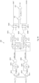
- Figures 4A-4C together illustrate a schematic view of a decoding circuit 400 for decoding the Isolated SPI signal of Figure 3 , in an embodiment.
- the circuit in Figure 4A is the signal detection and synchronization circuit of the decoding circuit 400.
- the signal detection and synchronization circuit detects (e.g., decodes) the digital bits carried by the Isolated SPI signal, and generates a three-pin output signal that includes a first data signal labeled as DIRECT, a second data signal labeled as REVERSE, and a synchronization signal labeled as SCK in Figure 4A .
- the positive signal and the negative signal of the Isolated SPI signal are connected to the input terminals PAD_P and PAD_N, respectively.
- the positive signal and the negative signal are compared by a comparator 401A to generate an output signal COMP_P, which is sent to an input terminal of an AND gate 405A.
- the output signal COMP_P is delayed by a delay element 403A (e.g., having a 20 ns delay), and the output of the delay element 403A is sent to another input terminal of the AND gate 405A.
- the delay element 403A and the AND gate 405A are used to remove effects of spurious signals (e.g., spurs) in the input signal at the input terminals PAD_P and PAD _N.
- the output signal of the AND gate 405A is labeled as COMP_P_DEGL.
- a similar circuit is used to generate an output signal COMP_N_DEGL, using a comparator 401B, a delay element 403B, and an AND gate 405B.
- the output signals COMP_P_DEGL and COMP_N_DEGL are decoded by the circuit formed by four flip-flops labeled as 1, 2, 3, and 4 in Figure 4A and two AND gates 407A and 407B.
- the output of the flip-flops 1, 2, 3, and 4 are labeled as O_1, O_2, O_3, and O_4, respectively.
- the reset terminals of the flip-flops 1, 2, 3, and 4 are connected to an RST_FF signal, which is generated in Figure 4B .
- the output of the AND gates 407A and 407B are sent to flip-flops 409A and 409B, respectively.
- the flip-flops 409A and 409B are driven by a signal CLK (e.g., a clock signal), which is generated in Figure 4C .
- CLK e.g., a clock signal
- the outputs of the flip-flops 409A and 409B are the output signals DIRECT and REVERSE, respectively.
- the outputs of the flip-flops 409A and 409B are processed by NOR gates 411 and 413 to generate the synchronization signal SCK.
- An input signal CLK _ORIG_N of the NOR gate 413 is generated in Figure 4C .
- the signals DIRECT, REVERSE, and SCK form the three-pin signal used in the BMICs 100.
- the signals DIRECT and REVERSE may be referred to as the data signals of the three-pin signal, and the signal SCK may be referred to as the synchronization signal
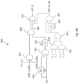
- Figure 4B illustrates the end detection and re-initialization circuit of the decoding circuit 400, which functions to detect the end of a bit frame, and in case a bit frame is not detected, a time-out function is performed to re-initialize the detection circuit in preparation for the processing of the next bit frame of the Isolated SPI signal.
- AND gates 421, 425, and 429 (some having inverted input terminals), an NOR gate 431, and delay elements 423 and 427 are used to generate the reset signal RST_FF.
- XOR gates 433 and 435, an OR gate 437, a delay element 439, and an AND gate 441 are used to generate a re-initialization signal when the end of a bit frame is not detected.
- the POR signal at an input terminal of the NOR gate 431 is a power-on reset signal generated by the BMIC 213 to ensure proper supply voltage.
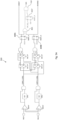
- Figure 4C illustrates the timing and oscillator control circuit of the decoding circuit 400.
- a plurality of logic gates e.g., OR gates 451, 455, an NOR gate 461, an AND gate 453, an inverter 463, a flip-flop 457, and a Set-Reset flip flop 465) are used to generate a control signal OSC_RST, which is then inverted to generate an oscillator enable signal OSC_EN.
- the oscillator enable signal OSC_EN enables or disables an oscillator 467.
- the oscillator 467 may be enabled only during time period used for decoding the digital bits, and may be disabled during other time period to save power consumption.
- the frequency of the oscillator 467 is the frequency that corresponds to the bit period T1.
- the oscillator 467 has a frequency of 8MHz.
- the frequency of the oscillator 467 is higher than the frequency that corresponds to the bit period T1.
- the output of the oscillator 467 is inverted, then sent to an input terminal of an AND gate 471.
- the oscillator enable signal OSC_EN is delayed by a delay element 469, and the output of the delay element 469 is sent to another input terminal of the AND gate 471.
- the output of the AND gate 471 is the signal CLK (e.g., a clock signal).
- Figure 4C further illustrates a counter 459, which is driven by a CLK_N signal (an inverted CLK signal) and is resets by a reset signal RST_CNT.
- the counter output is equal to one, the signal CNT_EQ_1 has a logic high value, otherwise it has a logic low value.
- the counter output is compared with 2 to set the value of the signal CNT_EQ_2.
- the signals O_3 _PLS and O4_PLS are derived from the signals O_3 and O_4, respectively.
- the signal O_3 _PLS is generated by performing a logic AND operation on the signal O_3 and an inverted and delayed version (e.g., delayed by a few nanoseconds) of the signal O_3.
- the signal O_4_PLS is generated similarly use the logic AND operation.
- Figure 4D illustrates a timing diagram for the decoding circuit 400 of Figures 4A-4C , in an embodiment.
- the signal labeled as PAD_ISO_P_RX at the top of Figure 4D illustrates the positive signal of the received Isolated SPI signal.
- the signals labeled as DIRECT, REVERSE, and SCK at the bottom of Figure 4D show the three-pin signal generated by the decoding circuit 400.
- the first bit frame of the received Isolated SPI signal carries a bit "1," and the second bit frame carries a bit "0.”
- the decoding circuit 400 For bit frame that carries a bit "1," the decoding circuit 400 generates a positive pulse in the signal DIRECT during that bit frame.
- the positive pulse has a same duration (e.g., 125 ns) as the bit period.
- the positive pulse in the signal DIRECT is generated near the end of the bit period of the bit frame carrying a bit "1," and as a result, the rising edge of the positive pulse is generated shortly before the start of the idle period of the bit frame, and the falling edge of the positive pulse is generated shortly before the end of the idle period of the bit frame.
- the signal DIRECT stays at a logic low value at time instants outside the positive pulse in the signal DIRECT.
- the decoding circuit 400 For each positive pulse generated in the signal DIRECT, the decoding circuit 400 generates a corresponding positive pulse in the synchronization signal SCK, which has a shorter duration than, and is located within the duration of, the positive pulse in the signal DIRECT.
- the signal DIRECT is sampled at the rising edge of the positive pulse in the synchronization signal SCK: a logic high value at the rising edge indicates a bit "1," and a logic low value at the rising edge indicates a bit "0.”
- the decoding circuit 400 For each bit frame that carries a bit "0,” the decoding circuit 400 generates a positive pulse in the signal REVERSE during that bit frame, which positive pulse is generated near the end of the bit period of the bit frame carrying the bit "0," and as a result, the rising edge of the positive pulse is generated shortly before the start of the idle period of the bit frame, and the falling edge of the positive pulse is generated shortly before the end of the idle period of the bit frame.
- the signal REVERSE remains at a logic low value at time instants outside the positive pulse in the signal REVERSE.
- the signal labeled as PAD_ISO_P_TX at the bottom of Figure 4D illustrates the positive signal of the Isolated SPI signal converted from the three-pin signal (e.g., DIRECT, REVERSE, and SCK), which corresponds to the output of the format convert 109A or 109B.
- the three-pin signal e.g., DIRECT, REVERSE, and SCK
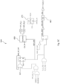
- FIGs 5A-5C together illustrate a schematic view of a decoding circuit 500 for decoding the Isolated SPI signal of Figure 3 , in another embodiment.
- the decoding circuit 500 uses an oscillator 467 (see Figure 5C ) having a frequency that is twice the frequency corresponding to the bit period of the Isolated SPI signal. For example, if the bit period is 125 ns (which corresponds to one clock cycle of an 8 MHz clock), then the oscillator 467 has a frequency of 16MHz.
- the circuit in Figure 5A is the signal detection and synchronization circuit of the decoding circuit 500, which is similar to that in Figure 4A .
- the flip-flops 409A and 409B are driven by a GCLK signal, which is generated in Figure 5C .
- the synchronization signal SCK of the three-pin signal is generated using an OR gate 415, an AND gate 419, and a flip-flop 417.
- Figure 5B illustrates the end detection and re-initialization circuit of the decoding circuit 500, which is the same as that in Figure 4B .
- Figure 5C illustrates the timing and oscillator control circuit of the decoding circuit 500, which is similar to that in Figure 4C , but with the output of the oscillator 467 gated by a clock gating circuit 473 to generate the GCLK signal.
- the clock gating circuit 473 comprises a latch and an AND gate, and is configured to receive a clock signal and generates a gated clock signal according to an enable signal.
- the clock gating circuit 473 is enabled by a CNT(0)_N signal, where the CNT(0)_N signal has a logic high value when the least significant bit (LSB) of the counter 459 is zero, and has a logic low value when the LSB of the counter 459 is one.
- LSB least significant bit
- Figure 5D illustrates a timing diagram for the decoding circuit of Figures 5A-5C , in an embodiment.
- the timing diagram in Figure 5D shows various signals generated by the decoding circuit 500 when decoding the Isolated SPI signal of Figure 3 . Details are similar to those in Figure 4D , thus not repeated.
- Figure 5E illustrates a timing diagram for the decoding circuit of Figures 5A-5C , in another embodiment.
- a modified version of the Isolated SPI signal is sent as the input signal to the decoding circuit 500.
- the modified version of the Isolated SPI signal is illustrated by the top signal in Figure 5E .
- the idle period of the modified Isolated SPI signal has a duration of 62.5 ns, which is half of the duration of the bit period 125 ns.
- This modified Isolated SPI signal allows for even higher data transmission rate due to a shorter bit frame.
- the decoding circuit 500 is able to decode the modified Isolated SPI signal correctly, as illustrated by Figure 5E .
- Figure 6 illustrates a frame structure 601 for the measurement data of each battery pack, in an embodiment.
- the digital control circuit 103 of each slave BMIC 213S packs all the measurement data from the battery pack 110 into a frame (e.g., a single frame), and send the frame in a burst mode to the MCU 211.
- Figure 6 also illustrates the burst request 603 (e.g., a request message indicated as "BURST REQ BY MCU") from the MCU 211, and a pulse 605 indicating the duration of the burst mode transmission of the battery measurement data.
- the burst mode transmission differs from a non-burst mode transmission, where in the non-burst mode transmission, the measurement data from each cell 111 of the battery pack 110 is packed into a frame (also referred to as a classic frame to distinguish from the burst mode frame structure 601) and transmitted. Since each frame has its overhead bits (e.g., bits used for forming the frame structure but not used for carrying the payload data such as battery measurement data), and since each battery pack 110 has multiple cells 111, the overhead bits reduce the number of payload bits (e.g., the battery measurement data) that could be transmitted per second.
- the overhead bits e.g., bits used for forming the frame structure but not used for carrying the payload data such as battery measurement data
- the frame structure 601 disclosed herein by packing measurement from all cells 111 of a battery pack 110 into a single frame, reduces the number of overhead bits needed to transmit all the measurement data, thereby increasing the payload data rate.
- the frame structure 601 is able to transmit all of the measurement data from a battery pack that has up to 18 batter cells (e.g., 18 voltage measurements for the 18 cells), 9 temperature sensors (e.g., 9 temperature measurements), and 3 voltage sum signals.
- Figure 6 also shows the data fields within the frame structure 601.
- a data field PA may be used to indicate whether the current frame of data is a command sent by a master unit or an answer (e.g., battery measurement data) from a slave unit.
- the data field PA may have one bit and indicate that the frame comprises a command sent by a master unit (e.g., PA is set to 1) or an answer sent by a slave unit (e.g., PA is set to 0).
- a data field BURST indicates whether the current frame is a long frame having the burst mode frame structure 601, or a classic frame (e.g., for backward compatibility purpose).
- the data field BURST may have one bit and indicate that the frame comprises an answer with classic frame (e.g., BURST is set to 0) or an answer with a long frame format (e.g., BURST is set to 1).
- a data field DEV ID identifies the device ID of the slave BMIC 213S reporting its battery measurement data.
- the data field DEV ID may have between 4 and 8 bits, e.g., 6 bits.
- a data field CELLS ENABLED indicates which cells are enabled (e.g., measured).
- the data field CELLS ENABLED may indicate bit-by-bit which cells are enabled. For example, if the first cell of the battery pack is enabled, then the first bit in this data field has a value of 1.
- the data field CELLS ENABLED may have between 4 and 32 bits, e.g., 18 bits, thereby supporting 18 voltage measurement values for 18 cells of the battery pack.
- a data field TEMP ENABLED indicates which temperature sensors are enabled (e.g., measured).
- the data field TEMP ENABLED may indicate bit-by-bit which sensors are enabled.
- the data field TEMP ENABLED may have between 4 and 16 bits, e.g., 9 bits.
- the voltage measurement data from all of the cells in the battery pack are processed by a data compression method to reduce the number of bits transmitted. For example, to compress the 18 voltage measurement values for the 18 cells of the battery pack, the minimum value of the 18 voltage measurement values is determined, and 18 voltage difference values are calculated by subtracting the minimum value from the 18 voltage measurement values. Since the voltage differences between the battery cells within a battery pack tend to be small, the 18 voltage difference values are small and can be represented by fewer bits than the original 18 voltage measurement values.
- the minimum value and the (e.g., 18) voltage difference values are sent.
- the minimum value is stored in the field MIN VALUE, e.g., having 16 bits.
- each of the (e.g., 18) voltage difference values is assigned a respective field DELTA, such as fields "DELTA 1" to "DELTA 18" for 18 voltage difference values, wherein each field DELTA has a given number N bits.
- the number N is indicated by a data field DELTA N BITS, e.g., having four-bits.
- DELTA N BITS e.g., having four-bits.
- up to 18 data fields labeled as data field DELTA 1 - DELTA 18 and each having a field width of N+1 bit, are used to store up to 18 voltage difference values. Note that only measurement data from battery cells indicated as being enabled by the data field CELLS ENABLED may be packed in the frame structure 601, this further increases the pay load efficiency of the frame structure 601.
- a data field SUMS comprises measurements for up to three voltage sum signals, where each voltage sum signal is assigned a given number of bits, such as 16 bits.
- a data field TEMPERATURES stores, e.g., up to nine, temperature measurement data, where each temperature measurement is assigned a given number of bits, such as 12 bits. Specifically, only temperature measurement data indicated as being enabled by the data field TEMPERATURE ENABLED may be packed in the field TEMPERATURES.
- a CRC data field includes a plurality of cyclic redundancy check (CRC) bits for the frame structure 601, such as 10 CRC bits.
- CRC cyclic redundancy check
- a CRC with Hamming Distance of 3 may be used.
- the disclosed bit frame (e.g., with a short idle period) of the Isolated SPI signal improves data rate at the physical layer.
- the disclosed burst mode frame structure improves data rate at the data link layer.
- the total time needed for the MCU 211 to request and receive measurement data from all 62 battery packs may be estimated as follows: assuming that the request message from the MCU is a data frame containing 40 bits, an interframe duration (e.g., a waiting period between frames of data transmitted and/or received) of 1 ⁇ s is used between data frames, and the Isolated SPI signal has a bit frame of 250 ns.
- the maximum number of bits in the burst frame structure 601 is 510 bits.
- the MCU 211 is able to collect measurement data from all 62 battery packs in less than 10ms.
- the number of bits needed for the voltage difference e.g., indicated by the DELTA N BITS data field
- the communication time used for sending the DELTA N BITS data field and the DELTA1 - DELTA 18 data field is greatly reduced, which saves power consumption, or alternatively, the data transmission time saved can be used to transmit other types of measurement data.
- the time saving is used to transmit the same measurement data from the battery packs at higher frequency, which enables reconstruction of the state (e.g., condition) of the battery packs with higher precision.
- the ability to collect measurements from all battery packs in such a short period of time allows the battery management system 200 to achieve real-time or near real-time control of the battery packs to improve reliability, safety, and performance of the system.
- the disclosed Isolated SPI signal uses a differential signal for data communication, which provides easy galvanic isolation between different voltage domains.
- the Isolated SPI signal has a short bit frame duration (e.g., bit period and idle period having equal duration) to increase the data rate transmitted through the Isolated SPI interface.
- Various embodiments of decoding circuits for the Isolated SPI signal are disclosed.
- a burst mode frame structure is disclosed. In the burst mode, the measurement from all cells within a battery is packed into a single frame (e.g., to save overhead bits) for transmission.
- the disclosed circuits and protocol allow for high speed data communication between the MCU 211 and the battery packs (through the slave BMICs 213 S) for better battery management performance.
- an integrated circuit (IC) device includes: a first plurality of input/output (I/O) pins; a first interface circuit coupled to the first plurality of I/O pins, wherein the first interface circuit comprises a first decoding circuit and a first format converter; a second plurality of I/O pins; a second interface circuit coupled to the second plurality of I/O pins, wherein the second interface circuit comprises a second decoding circuit and a second format converter; a first data bus coupled between outputs of the first decoding circuit and inputs of the second format converter; a second data bus coupled between outputs of the second decoding circuit and inputs of the first format converter; and a digital control circuit coupled to the first data bus and the second data bus, wherein each of the first decoding circuit and the second decoding circuit is configured to decode an Isolated Serial Peripheral Interface (SPI) signal into a three-pin signal, wherein the Isolated SPI signal is a differential signal comprising a positive signal and a complementary negative
- SPI I
- Example 2 The IC device of Example 1, wherein the digital control circuit is configured to convert the three-pin signal from the first data bus or the second data bus into digital bits by sampling the first data signal of the three-pin signal at rising edges of the synchronization signal.
- Example 3 The IC device of Example 1, wherein in a bit frame, the idle period follows the bit period, wherein during the bit period, the positive signal changes from a positive value to a negative value, or vice versa, wherein in the idle period, the positive signal remains at a zero value.
- Example 4 The IC device of Example 3, wherein for each bit frame of the Isolated SPI signal, each of the first decoding circuit and the second decoding circuit is configured to decode the Isolated SPI signal by: generating a positive pulse in the first data signal if the bit frame carries a digital bit of one, or generating a positive pulse in the second data signal if the bit frame carries a digital bit of zero, wherein a rising edge of the positive pulse is generated before a start of the idle period of the bit frame, and a falling edge of the positive pulse is generated before an end of the idle period of the bit frame; and generating a positive synchronization pulse in the synchronization signal, wherein a rising edge of the positive synchronization pulse is between the rising edge and the falling edge of the positive pulse in the first data signal or in the second data signal.
- Example 5 The IC device of Example 4, wherein a duration of the positive pulse is the same as that of the bit period.
- Example 6 The IC device of Example 1, further comprising a third plurality of I/O pins, wherein the digital control circuit is couple to the third plurality of I/O pins and the first plurality of I/O pins.
- Example 7 The IC device of Example 6, wherein the IC device is configured to function in a master mode or a slave mode, wherein in the master mode, the IC device is configured to: receive a standard SPI signal through the first plurality of I/O pins and the third plurality of I/O pins; convert, by the digital control circuit, the standard SPI signal into the three-pin signal; send the three-pin signal to the second format converter through the first data bus; convert, by the second format converter, the three-pin signal into a first Isolated SPI signal; and output the first Isolated SPI signal at the second plurality of I/O pins.
- Example 8 The IC device of Example 7, wherein in the master mode, the IC device is further configured to: receive, at the second plurality of I/O pins, a second Isolated SPI signal; decoding, by the second decoding circuit, the second Isolated SPI signal into the three-pin signal; receive, by the digital control circuit, the three-pin signal through the second data bus; convert, by the digital control circuit, the three-pin signal into the standard SPI signal; and output the standard SPI signal at the first plurality of I/O pins and the third plurality of I/O pins.
- Example 9 The IC device of Example 8, wherein in the slave mode, the IC device is configured to: receive a third Isolated SPI signal at the first plurality of I/O pins; decode, by the first decoding circuit, the third Isolated SPI signal into the three-pin signal; convert, by the digital control circuit, the three-pin signal into digital bits; process, by the digital control circuit, the digital bits; and relay the third isolated SPI signal by outputting the third Isolated SPI signal at the second plurality of I/O pins.
- Example 10 The IC device of Example 9, where the digital bits comprises an identification (ID) number, wherein the digital control circuit is configured to process the digital bits by: comparing the ID number with a device ID of the IC device; and in response to determining that the ID number matches the device ID of the IC device, sending a frame of data to the first plurality of I/O pins by: converting the frame of data into the three-pin signal; and sending the three-pin signal to the first format converter, wherein the first format converter is configured to convert the three-pin signal into a fourth Isolated SPI signal and output the fourth Isolated SPI signal at the first plurality of I/O pins.
- ID identification
- Example 11 The IC device of Example 9, wherein in the slave mode, the IC device is further configured to: receive, at the second plurality of I/O pins, a fifth Isolated SPI signal; and relay the fifth Isolated SPI signal by outputting the fifth Isolated SPI signal at the first plurality of I/O pins.
- a battery management system includes: a controller; a master battery management integrated circuit (BMIC) device coupled to the controller and configured to communicate with the controller through a standard Serial Peripheral Interface (SPI) protocol; a first slave BMIC device, wherein a first Isolated SPI interface of the first slave BMIC device is coupled to an Isolated SPI interface of the master BMIC through galvanic isolation, wherein the first slave BMIC device is configured to be coupled to a first battery pack, wherein the Isolated SPI interface is a two-pin communication interface using a differential signal comprising a positive signal and a complementary negative signal, wherein a bit frame of the positive signal includes a bit period followed by an idle period that has a same duration as the bit period; and a second slave BMIC device, wherein a first Isolated SPI interface of the second slave BMIC device is coupled to a second Isolated SPI interface of the first slave BMIC device through galvanic isolation, wherein the second slave BMIC device is configured to be coupled to
- Example 13 The battery management system of Example 12, wherein the first Isolated SPI interface of the first slave BMIC device is coupled to the Isolated SPI interface of the master BMIC through a first transformer, wherein the first Isolated SPI interface of the second slave BMIC device is coupled to the second Isolated SPI interface of the first slave BMIC device through a second transformer or through capacitors.
- Example 14 The battery management system of Example 12, wherein the controller and the master BMIC device are disposed on a first printed circuit board (PCB), and the first slave BMIC device is disposed on a second PCB, wherein the first PCB and the second PCB are in different power domains.
- PCB printed circuit board
- Example 15 The battery management system of Example 12, wherein the battery management system is configured to: send, by the controller, a first standard SPI signal to the master BMIC device, the first standard SPI signal comprising a message that includes a request for battery measurement and an identification (ID) number; convert, by the master BMIC device, the standard SPI signal into a first Isolated SPI signal at the Isolated SPI interface of the master BMIC device; receive, by the first slave BMIC device, the first Isolated SPI signal through the first Isolated SPI interface of the first slave BMIC device; relay, by the first slave BMIC device, the first Isolated SPI signal to the second Isolated SPI interface of the first slave BMIC device; decode, by the first slave BMIC device, the first Isolated SPI signal into digital bits; and process, by the first slave BMIC device, the digital bits, comprising: comparing the ID number with a device ID of the first slave BMIC device; and in response to determining that the ID number matches the device ID, sending measurement data of the
- Example 16 The battery management system of Example 15, wherein the first battery pack comprises a plurality of battery cells, wherein the measurement data include measurements for the plurality of battery cells, wherein measurements for the plurality of battery cells are packed in a single data frame, wherein the first slave BMIC device is configured to send the single data frame in a burst mode transmission.
- a battery system includes: a battery pack comprising a plurality of battery cells; and a battery management integrated circuit (BMIC) device coupled to the batter pack, the BMIC device comprising: a first plurality of input/output (I/O) pins; a first interface circuit coupled to the first plurality of I/O pins, wherein the first interface circuit comprises a first decoding circuit and a first format converter; a second plurality of I/O pins; a second interface circuit coupled to the second plurality of I/O pins, wherein the second interface circuit comprises a second decoding circuit and a second format converter; a first data bus coupled between outputs of the first decoding circuit and inputs of the second format converter; a second data bus coupled between outputs of the second decoding circuit and inputs of the first format converter; a digital control circuit coupled to the first data bus and the second data bus; and analog-to-digital converters (ADCs) coupled between the digital control circuit and the battery pack, wherein each of the first decoding
- ADCs
- Example 18 The battery system of Example 17, wherein in a bit frame of the positive signal, the idle period follows the bit period, wherein during the bit period, the positive signal transitions from a positive value to a negative value, or vice versa, wherein in the idle period, the positive signal remains at a zero value, wherein the digital control circuit is configured to convert the three-pin signal into digital bits by sampling the first data signal of the three-pin signal at rising edges of the synchronization signal.
- Example 19 The battery system of Example 18, wherein for each bit frame of the Isolated SPI signal, each of the first decoding circuit and the second decoding circuit is configured to decode the Isolated SPI signal by: generating a positive pulse in the first data signal if the bit frame carries a digital bit of one, or generating a positive pulse in the second data signal if the bit frame carries a digital bit of zero, wherein a rising edge of the positive pulse is generated before a start of the idle period of the bit frame, and a falling edge of the positive pulse is generated before an end of the idle period of the bit frame; and generating a positive synchronization pulse in the synchronization signal, wherein a rising edge of the positive synchronization pulse is between the rising edge and the falling edge of the positive pulse in the first data signal or in the second data signal.
- Example 20 The battery system of Example 17, wherein the BMIC device is configured to: collect, by the digital control circuit, outputs from the ADCs, wherein the outputs from the ADCs comprise measurements for the plurality of battery cells of the battery pack; compress, by the digital control circuit, the measurements for the plurality of battery cells into few data bits using a data compression method based on voltage differences among the plurality of battery cells; pack, by the digital control circuit, the compressed measurements for the plurality of battery cells in a data frame; and send, by the first interface circuit, the data frame in a burst mode of transmission as a first Isolated SPI signal.
Landscapes
- Engineering & Computer Science (AREA)
- Theoretical Computer Science (AREA)
- General Engineering & Computer Science (AREA)
- Physics & Mathematics (AREA)
- General Physics & Mathematics (AREA)
- Computer Hardware Design (AREA)
- Computer Networks & Wireless Communication (AREA)
- Signal Processing (AREA)
- Mathematical Physics (AREA)
- Battery Mounting, Suspending (AREA)
- Secondary Cells (AREA)
Abstract
Description
- The present invention relates generally to battery management systems (BMSs) and battery management integrated circuit (BMIC) devices.
- Battery packs are used in a wide variety of electrical systems and applications, such as full electric (FE) vehicles, hybrid electric (HE) vehicles, backup energy storage systems, uninterruptible power supply (UPS) units, e-bikes, e-scooters, portable and semi-portable equipment. The evolving technology of the electrical systems makes improved performance of battery management systems (BMSs) a desirable feature in order to facilitate safe, reliable and cost-efficient battery operation.
- Battery management integrated circuit (BMIC) devices are used in battery management system. For example, in FE vehicle or hybrid electric vehicle applications, to manage all battery packs installed in the vehicle, a lot of BMIC devices are used in the battery management system. Each battery pack is coupled to a BMIC device, which BMIC device manages the battery cells in the battery back. One of the tasks of the BMIC is to perform very precise cell voltage measurements and communicate the measurements to a micro-controller (MCU) of the battery management system as quickly as possible, in order to maintain all cells voltages as close as possible to increase battery performance.
- As the number of battery packs used in the electrical vehicles increases, communicating the measurements from all of the battery packs to the MCU in a timely manner may become a challenge. There is a need in the art for BMIC devices that support high speed data communication between the MCU and the BMIC devices.
- In some embodiments, an integrated circuit (IC) device includes: a first plurality of input/output (I/O) pins; a first interface circuit coupled to the first plurality of I/O pins, wherein the first interface circuit comprises a first decoding circuit and a first format converter; a second plurality of I/O pins; a second interface circuit coupled to the second plurality of I/O pins, wherein the second interface circuit comprises a second decoding circuit and a second format converter; a first data bus coupled between outputs of the first decoding circuit and inputs of the second format converter; a second data bus coupled between outputs of the second decoding circuit and inputs of the first format converter; and a digital control circuit coupled to the first data bus and the second data bus, wherein each of the first decoding circuit and the second decoding circuit is configured to decode an Isolated Serial Peripheral Interface (SPI) signal into a three-pin signal, wherein the Isolated SPI signal is a differential signal comprising a positive signal and a complementary negative signal, wherein a bit frame of the positive signal includes a bit period and an idle period that have a same duration, wherein the three-pin signal includes a first data signal, a second data signal, and a synchronization signal, wherein each of the first format converter and the second format converter is configured to convert the three-pin signal into the Isolated SPI signal.
- In some embodiments, a battery management system includes: a controller; a master battery management integrated circuit (BMIC) device coupled to the controller and configured to communicate with the controller through a standard Serial Peripheral Interface (SPI) protocol; a first slave BMIC device, wherein a first Isolated SPI interface of the first slave BMIC device is coupled to an Isolated SPI interface of the master BMIC through galvanic isolation, wherein the first slave BMIC device is configured to be coupled to a first battery pack, wherein the Isolated SPI interface is a two-pin communication interface using a differential signal comprising a positive signal and a complementary negative signal, wherein a bit frame of the positive signal includes a bit period followed by an idle period that has a same duration as the bit period; and a second slave BMIC device, wherein a first Isolated SPI interface of the second slave BMIC device is coupled to a second Isolated SPI interface of the first slave BMIC device through galvanic isolation, wherein the second slave BMIC device is configured to be coupled to a second battery pack.
- In some embodiments, a battery system includes: a battery pack comprising a plurality of battery cells; and a battery management integrated circuit (BMIC) device coupled to the batter pack, the BMIC device comprising: a first plurality of input/output (I/O) pins; a first interface circuit coupled to the first plurality of I/O pins, wherein the first interface circuit comprises a first decoding circuit and a first format converter; a second plurality of I/O pins; a second interface circuit coupled to the second plurality of I/O pins, wherein the second interface circuit comprises a second decoding circuit and a second format converter; a first data bus coupled between outputs of the first decoding circuit and inputs of the second format converter; a second data bus coupled between outputs of the second decoding circuit and inputs of the first format converter; a digital control circuit coupled to the first data bus and the second data bus; and analog-to-digital converters (ADCs) coupled between the digital control circuit and the battery pack, wherein each of the first decoding circuit and the second decoding circuit is configured to decode an Isolated Serial Peripheral Interface (SPI) signal into a three-pin signal, wherein the Isolated SPI signal is a differential signal comprising a positive signal and a complementary negative signal, wherein a bit frame of the positive signal includes a bit period and an idle period that have a same duration, wherein the three-pin signal includes a first data signal, a second data signal, and a synchronization signal, wherein each of the first format converter and the second format converter is configured to convert the three-pin signal into the Isolated SPI signal.
- The details of one or more embodiments of the invention are set forth in the accompanying drawings and the description below. Other features, objects, and advantages of the invention will be apparent from the description and drawings, and from the claims. In the figures, identical reference symbols generally designate the same component parts throughout the various views, which will generally not be re-described in the interest of brevity. For a more complete understanding of the invention, reference is now made to the following descriptions taken in conjunction with the accompanying drawings, in which:
-
Figure 1 illustrates a block diagram of a battery system including a battery management integrated circuit (BMIC) and a battery pack, in an embodiment; -
Figure 2 illustrates a battery management system (BMS), in an embodiment; -
Figure 3 illustrates an Isolated Serial Peripheral Interface (SPI) signal, in an embodiment; -
Figures 4A-4C together illustrate a schematic view of a decoding circuit for decoding the Isolated SPI signal ofFigure 3 , in an embodiment; -
Figure 4D illustrates a timing diagram for the decoding circuit ofFigures 4A-4C , in an embodiment; -
Figures 5A-5C together illustrate a schematic view of a decoding circuit for decoding the Isolated SPI signal ofFigure 3 , in another embodiment; -
Figure 5D illustrates a timing diagram for the decoding circuit ofFigures 5A-5C , in an embodiment; -
Figure 5E illustrates a timing diagram for the decoding circuit ofFigures 5A-5C , in another embodiment; and -
Figure 6 illustrates a frame structure for the measurement data of each battery pack, in an embodiment. - The making and using of the presently preferred embodiments are discussed in detail below. It should be appreciated, however, that the present invention provides many applicable inventive concepts that can be embodied in a wide variety of specific contexts. The specific embodiments discussed are merely illustrative of specific ways to make and use the invention, and do not limit the scope of the invention.
- The present invention will be described with respect to exemplary embodiments in a specific context, namely battery management integrated circuits (BMICs) and battery management systems (BMSs).
-
Figure 1 illustrates a block diagram of abattery system 150 that includes a battery management integrated circuit (BMIC) 100 (may also be referred to as a BMIC device) and abattery pack 110, in an embodiment. Thebattery pack 110 is coupled to theBMIC 100 and is managed by theBMIC 100. In some embodiments, the BMIC 100 is installed (e.g., bonded) on the printed circuit board (PCB) board of thebattery pack 110. - As illustrated in
Figure 1 , the battery pack 110 (may also be referred to as abattery 110 for simplicity) includes a plurality of battery cells 111 (may also be referred to ascells 111 for simplicity). Thebattery cells 111 may be coupled in series and/or in parallel to provide a desired supply voltage and/or supply current of thebattery pack 110. The number ofbattery cells 111 may vary from, e.g., a few cells to tens of (e.g., about 20) cells.Figure 1 further illustrates abus 113 in thebattery pack 110. Thebus 113 couples thebattery cells 111 to the analog-to-digital converters (ADCs) 107 of theBMIC 100. - As illustrated in
Figure 1 , theBMIC 100 includes afirst interface circuit 101, asecond interface circuit 105, adigital control circuit 103, and a plurality of analog-to-digital converters (ADCs) 107. In the block diagram ofFigure 1 , the plurality ofADCs 107 are illustrated as one block, with the understanding thatmultiple ADCs 107 may be included in theBMIC 100. Note that for simplicity, not all features of theBMIC 100 are illustrated inFigure 1 . The BMIC 100 is used as a transceiver device to transmit and receive a serial data stream in a half-duplex mode, in some embodiments. In addition, theBMIC 100 may be used as an interface device to connect a device with a Serial Peripheral Interface (SPI) interface (may also be referred to as a standard SPI interface to distinguish from the Isolated SPI interface discussed herein) to another device with an Isolated SPI interface, in some embodiments. The SPI interface is an industry standard interface that communicates with a four-line data bus labeled as, e.g., SDI, SDO, NCS, SCK. The Isolated SPI interface described herein is a custom interface that communicates with a two-line data bus (e.g., for carrying a differential signal). The BMIC 100 may be set to work in a master mode or a slave mode. Details are discussed hereinafter. - In
Figure 1 , thefirst interface circuit 101 includes adecoding circuit 106A and aformat converter 109A. Thesecond interface circuit 105 includes adecoding circuit 106B and aformat converter 109B. Thedecoding circuit 106A in thefirst interface circuit 101 is the same as thedecoding circuit 106B in thesecond interface circuit 105, and may be collectively referred to as decoding circuits 106, in some embodiments. Theformat converters 109A in thefirst interface circuit 101 is the same as theformat converter 109B in thesecond interface circuit 105, and may be collectively referred to as format converters 109, in some embodiments. As illustrated inFigure 1 , afirst data bus 102, which has three signal lines labeled as DIRECT, REVERSE, and SCK inFigure 1 , is coupled between the output terminals of thedecoding circuit 106A and the input terminals of theformat converter 109B. Asecond data bus 104, which also has three signal lines labeled as DIRECT, REVERSE, and SCK inFigure 1 , is coupled between the output terminals of thedecoding circuit 106B and the input terminals of theformat converter 109A. - The
decoding circuit 106A is configured to receive an Isolated SPI signal from two input/output (I/O) pins of theBMIC 100 labeled as ISOLP _SDI and ISOLM _NCS inFigure 1 , and is configured to decode the received Isolated SPI signal into a three-pin signal (e.g., a signal transmitted on three signal lines), which three-pin signal is sent through thefirst data bus 102 to theformat converter 109B. The Isolated SPI signal is a differential signal that includes a positive signal and a complementary negative signal for transmitting a serial data stream. Details of the Isolated SPI signal are described hereinafter with reference toFigure 3 . Details of the three-pin signal are described hereinafter with reference toFigure 4D . Various embodiments of the decoding circuit 106 are discussed hereinafter with reference toFigures 4A-4C andFigures 5A-5C . Theformat converter 109B converts the three-pin signal received from thefirst data bus 102 back into the Isolated SPI signal, and sends the converted Isolated SPI signal to the I/O pins of theBMIC 100 labeled as ISOHP and ISOHM inFigure 1 . - Similarly, the
decoding circuit 106B is configured to receive an Isolated SPI signal from the I/O pins of theBMIC 100 labeled as ISOHP and ISOHM inFigure 1 , and is configured to decode the received Isolated SPI signal into the three-pin signal, which three-pin signal is sent through thesecond data bus 104 to theformat converter 109A. Theformat converter 109A converts the three-pin signal received from thesecond data bus 104 back into the Isolated SPI signal, and sends the converted Isolated SPI signal to the I/O pins of theBMIC 100 labeled as ISOLP_SDI and ISOLM NCS inFigure 1 . - The
digital control circuit 103 is coupled to thefirst data bus 102 and thesecond data bus 104. Thedigital control circuit 103 may be or include a processor, a digital logic, combinations thereof, or the like. Thedigital control circuit 103 converts the three-pin signal transmitted on thefirst data bus 102 or thesecond data bus 104 into a serial data stream (e.g., a one-bit data stream) for processing by thedigital control circuit 103. In addition, thedigital control circuit 103 can also convert a serial data stream generated (or received) by thedigital control circuit 103 into the three-pin signal for transmission on thefirst data bus 102 or thesecond data bus 104. In other words, thedigital control circuit 103 can translate between the three-pin signal and a serial data stream. - Still referring to
Figure 1 , thedigital control circuit 103 is also coupled to the I/O pins labeled as ISOLP _SDI, ISOLM NCS, SDO, and SCK. When theBMIC 100 works in master mode and when a standard SPI signal (which may include four signal lines such as SDI, NCS, SDO, and SCK) is applied at the I/O pins labeled as ISOLP_SDI, ISOLM _NCS, SDO, and SCK, thedigital control circuit 103 converts the standard SPI signal into the three-pin signal for transmission on, e.g., thefirst data bus 102. Conversely, when a three-pin signal is received by thedigital control circuit 103, thedigital control circuit 103 can convert the three-pin signal into the standard SPI signal and output the standard SPI signal at the I/O pins labeled as ISOLP_SDI, ISOLM _NCS, SDO, and SCK. When theBMIC 100 works in slave mode, the I/O pins ISOLP _SDI and ISOLM _NCS are used as the I/O pins of an Isolated SPI interfaces of theBMIC 100 to transmit/receive a differential signal. The I/O pins ISOHP and ISOHM of theBMIC 100 are used as the I/O pins of another Isolated SPI interface of theBMIC 100. - In the example of
Figure 1 , theBMIC 100 further includes a plurality ofADCs 107. Preferably each of thebattery cells 111 is coupled to arespective ADC 107, such that all of thebattery cells 111 can be measured at the same time (e.g., simultaneously), in some embodiments. TheBMIC 100 may also have acontrol path 108 for controlling the operation of thebattery pack 110. In some embodiments, theBMIC 100 may control the internal switches/control circuits of thebattery pack 110, such that thebattery cells 111 are coupled torespective ADCs 107 through thebus 113, such that the voltage of eachindividual battery cell 111 is converted into digital data by arespective ADC 107. Although not shown, thebattery pack 110 may include other sensors for measuring other characteristics of thebattery pack 110, such as temperature sensors for measuring the temperature at different locations within thebattery pack 110. These sensors may also be coupled to thebus 113 such that the sensor outputs can be converted by theADCs 107 into digital data. -
Figure 2 illustrates a battery management system (BMS) 200, in an embodiment. TheBMS 200 includes a micro-controller (MCU) 211 and a plurality of BMICs 213 (e.g., 213M, 213SA, 213SB, and 213SC). In the illustrated embodiment, theBMICs 213 inFigure 2 are the same as theBMIC 100 inFigure 1 . One of theBMICs 213, labeled as 213M, is set to a master mode and may be referred to asmaster BMIC 213M, and theother BMICs 213, labeled as 213SA, 213SB, and 213SC, are set to a slave mode and may be referred to as slave BMICs 213SA, 213SB, and 213SC. The mode of theBMIC 213 may be set by any suitable method. For example, selection between the master mode and the slave mode of theBMIC 213 may be achieved, e.g., by connecting a mode selection pin of theBMIC 213 to electrical ground or to a supply voltage VDD, or by setting an internal register bit (e.g., an EEPROM bit) of theBMIC 213 to zero or one. The slave BMICs 213SA, 213SB, and 213SC may be collectively referred to as slave BMICs 213S. The number of slave BMICs 213S illustrated inFigure 2 is merely a nonlimiting example, other numbers of slave BMICs 213S may also be used in theBMS 200, as skilled artisans readily appreciate. For simplicity, some of the I/O pins (e.g., SDO, SCK) of theBMIC 100 inFigure 1 are not illustrated for the slave BMICs 213S inFigure 2 . - The
BMS 200 is described below with respect to an example application, namely the battery management system in full electric (FE) vehicles or hybrid electric (HE) vehicles. The structure and principle of theBMS 200 may be used in other applications, as skilled artisans readily appreciate. In the example ofFigure 2 , theMCU 211 and themaster BMIC 213M may be located on the same printed circuit board (PCB), and the PCB is in a low voltage domain where power supplies with low voltages such as 3V, 5V, or the like are used. Themaster BMIC 213M is coupled to theMCU 211 through a standard SPI interface, and functions as an interface device between theMCU 211 and the slave BMICs 213S, which slave BMICs 213S communicate through a custom Isolated SPI interface. - As illustrated in
Figure 2 , the slave BMICs 213S are connected in a daisy chain configuration. Each of the slave BMICs 213S is located on a separate PCB and is connected to a respective battery pack 110 (seeFigure 1 ). Eachbattery pack 110 has a plurality ofbattery cells 111 coupled together to provide a high voltage of, e.g., 48 V. Therefore, the BMIC 213S are in ahigh voltage domain 220. In an FE vehicle or a HE vehicle, there are many battery packs 110, and each battery pack (with its respective slave BMIC 213 S) may be installed at a different location within the vehicle. The distance between the slave BMICs 213S may be as far as about 10 m. In addition, each PCB on which theBMIC 213 is bonded is powered by the corresponding battery pack 110 (e.g., the BMIC power supply pins are connected to the positive terminal and the negative terminal of the battery pack 110). The different power supplies on the different PCBs do not allow the usage of the standard SPI protocol to connect all the PCBs. Instead, a special (e.g., custom) communication protocol, which not only provides properly decoupling between the different PCBs, but is also robust to noise and compatible with high voltage applications, is used. The Isolated SPI protocol and the Isolated SPI interface described herein, which uses a pair of conductive lines (e.g., a twisted pair) to transmit a differential signal, are suitable for data transmission in these challenging environments. - Referring temporarily to
Figure 3 , which shows the Isolated SPI signal (which is a differential signal) used in the Isolated SPI protocol. The differential signal includes apositive signal 301 and a complementarynegative signal 303.Figure 3 shows two bit frames of the Isolated SPI signal, where each bit frame has a duration (referred to as a bit frame duration) of T. The first bit frame carries a digital bit of "1," and the second bit frame carries a digital bit of "0." As illustrated inFigure 3 , each bit frame includes a bit period T1 followed by an idle period T2. In the illustrated embodiment, the bit period T1 has the same duration as the idle period T2 (e.g., T1=T2). During the bit period T1, the positive signal has a stair shape, and changes from a positive value to a negative value, or vice versa. For thepositive signal 301 of the Isolated SPI signal, a transition from positive value to negative value in the bit period T1 indicates a digital bit of "1," and a transition from negative value to positive value in the bit period T1 indicates a digital bit of "0." Thepositive signal 301 has a fixed zero value during the idle period T2. Thenegative signal 303 is a mirror image (e.g., mirrored along the horizontal line indicating a value of zero) of thepositive signal 301. As an example, the Isolated SPI signal may have a bit duration T1 of 125 ns, which corresponds to one clock cycle of an 8 MHz clock, and the idle duration T2 is also 125 ns. Therefore, the bit frame of the above example is 250 ns. - The Isolated SPI signal show in
Figure 3 defines a bit frame T having equal durations for the bit period T1 and the idle period T2 (T1=T2). Compared with a baseline Isolated SPI signal where the idle period T2 is twice as long as the bit period T1, the Isolated SPI signal defined herein allows for higher data rate (e.g., 33.3% higher) than the baseline Isolated SPI signal. The shorter bit frame of the presently disclosed Isolated SPI signal may entail new decoding circuit for the Isolated SPI signal, due to the shorter idle period. Embodiments of the decoding circuit are discussed below with reference toFigures 4A-4C andFigures 5A-5C . Another advantage of the Isolated SPI signal is that by using differential signaling, the Isolated SPI signal allows for easy galvanic isolation between the PCBs using, e.g., transformers or capacitors. - The Isolated SPI signal shows in
Figure 3 improves data rate by reducing the idle period of the bit frame and by decoding the Isolated SPI signal with the new decoding circuit discussed hereinafter. This is more advantageous than a brute force solution, where the baseline Isolated SPI signal is scaled (e.g., shortened) by half, and the whole baseline decoding circuit is clocked at twice the original clock rate. This is because the higher clock rate of the brute force method may result in more reflections along transmission lines, possible unwanted signal filtering due to passive components and/or parasitic components, less inducted noise robustness along the cable, and dynamic power growth due to frequency increasing, which may require more expensive wires with better shielding, (expensive) electrical termination to avoid signal reflection, and/or modified board design. - Referring back to
Figure 2 , theMCU 211 may be an off-the-shelf micro-controller that has a standard SPI interface that communicates with I/O pins labeled as, e.g., SDI, SDO, SCK and NCS inFigure 2 . Themaster BMIC 213M communicates with theMCU 211 using the standard SPI protocol, and connects with theMCU 211 through I/O pins labeled as SDO, ISOLP_SDI, SCK, and ISOLM_NCS. In addition, themaster BMIC 213M communicates with the slave BMIC 213SA using the Isolated SPI protocol through an Isolated SPI interface of themaster BMIC 213M, which includes I/O pins of the master BMIC labeled as ISOHP and ISOHM. - In the example of
Figure 2 , the I/O pins ISOHP and ISOHM of themaster BMIC 213M are coupled to the I/O pins ISOLP_SDI and ISOLM_NCS of the slave BMIC 213SA through atransformer 231. Thetransformer 231 provides galvanic isolation between thelow voltage domain 210 and thehigh voltage domain 220. The slave BMICs 213S are connected in a daisy chain configuration, andcapacitors 215 are used between neighboring slave BMICs 213S to provide decoupling. Thecapacitors 215 between two neighboring slave BMICs 213S may be replaced by a transformer, as skilled artisans readily appreciate. The slave BMICs 213 S communicate with each other using the Isolated SPI protocol. For example, the I/O pins ISOLP _SDI and ISOLM _NCS of each slave BMIC 213S form a first Isolated SPI interface for communication with aprevious BMIC 213 in the daisy chain (or themaster BMIC 213M), and the I/O pins ISOHP and ISOHM of each slave BMIC 213S form a second Isolated SPI interface for communication with a subsequent slave BMIC 213S (if any) in the daisy chain. Although not shown inFigure 2 , each of the slave BMICs 213S is connected to a respective battery pack 110 (seeFigure 1 ), and provides measurements of therespective battery pack 110 to themaster BMIC 213M through the daisy chain connection using the Isolated SPI protocol. - Referring to
Figure 2 andFigure 1 , to collect measurement data from the battery packs 110 connected to the slave BMICs 213S, theMCU 211 sends a request message with a device identification (ID) number, which device ID number indicates which slave BMIC 213S should report (e.g., send back) the measurement data for itsrespective battery pack 110. In the illustrate embodiment, theBMS 200 works in a half-duplex mode. For example, theMCU 211 sends a request message with a device ID, then waits for answers from (e.g., the measurement data send by) the slave BMIC 213S having the device ID until a timeout happens. This process repeats until all the slave BMICs 213S sends back their measurement data. - In the example of
Figure 2 , the request message is communicated through the standard SPI interface of theMCU 211 to themaster BMIC 213M. Themaster BMIC 213M converts (e.g., translates) the standard SPI signal into a three-pin signal for transmission on the first data bus 102 (seeFigure 1 ) toward theformat converter 109B of themaster BMIC 213M. Theformat converter 109B converts the three-pin signal into an Isolated SPI signal (e.g., a differential signal) for transmission at the I/O pins ISOHP and ISOHM of themaster BMIC 213M. - The Isolated SPI signal from the
master BMIC 213M is coupled to the I/O pins ISOLP _SDI and ISOLM_NCS of the slave BMIC 213SA through thetransformer 231. Thedecoding circuit 106A of the slave BMIC 213SA decodes the received Isolated SPI signal into the three-pin signal and outputs the three-pin signal on thefirst data bus 102. Thedigital control circuit 103 of the slave BMIC 213SA converts the three-pin signal on thefirst data bus 102 into digital bits (thereby recovering the request message from the MCU 211) and processes the received request message. For example, thedigital control circuit 103 compares the device ID in the request message with its own device ID and determines if they match. If the ID numbers do not match, thedigital control circuit 103 ignores the request message. If the ID numbers match, thedigital control circuit 103 will transmit the measurement data of itsrespective battery pack 110 back to themaster BMIC 213M immediately. Theformat converter 109B of the slave BMIC 213SA converts the three-pin signal on thefirst data bus 102 back into the Isolated SPI signal for transmission on the I/O pins ISOHP and ISOHM toward the next slave BMIC 213SB, this may be referred to as "relaying the Isolated SPI signal" to the next slave BMIC 213S. The relaying of the Isolated SPI signal happens as soon as the Isolated SPI signal is received by each slave BMIC 213S, e.g., while thedigital control circuit 103 is processing the three-pin signal and regardless of whether the ID numbers match, in order to reduce the delay in the relaying of the Isolated SPI signal in the daisy chain. - Each of the slave BMICs 213SB and 213SC receives the relayed Isolated SPI signal from its preceding slave BMIC 213S in the daisy chain through, e.g., coupling of the
capacitors 215. The internal processing of the received Isolated SPI signal in the slave BMICs 213SB and 213SC is the same as that of the slave BMIC 213SA, thus not repeated. After the Isolated SPI signal propagates through the daisy chain and is received by the last slave BMIC 213SC, only one of the slave BMICs 213S (with the matching device ID) will transmit its battery measurement data to themaster BMIC 213M. - Without loss of generality, consider the example where the slave BMIC 213SC has a device ID matching that in the request message. When sending back the battery measurement data, the
control circuit 103 of the slave BMIC 213SC packs the measurement date in a data frame, and converts the digital bits in the data frame into the three-pin signal, which is send over thesecond data bus 104 to theformat converter 109A of the slave BMIC 213SC. Theformat converter 109A converts the three-pin signal into an Isolated SPI signal for transmission on the I/O pins ISOLP_SDI and ISOLM_NCS of the slave BMIC 213SC toward the slave BMIC 213SB. - The
decoding circuit 106B of the slave BMIC 213SB decodes the received Isolated SPI signal into a three-pin signal, which is sent to theformat converter 109A through thesecond data bus 104. Theformat converter 109A converts the three-pin signal back into the Isolated SPI signal for transmission on the I/O pins ISOLP SDI and ISOLM NCS of the slave BMIC 213SB toward the slave BMIC 213SA. In other words, the slave BMIC 213SB relays the Isolated SPI signal toward the slave BMIC 213SA and themaster BMIC 213M. - The slave BMIC 213SA relays the received Isolated SPI signal toward the
master BMIC 213M. The processing is the same as or similar to that of the slave BMIC 213SB, thus not repeated. - The
master BMIC 213M receives the Isolated SPI signal at the I/O pins ISOHP and ISOHM through thetransformer 231. Thedecoding circuit 106B of themaster BMIC 213M decodes the received Isolated SPI signal into a three-pin signal, which is converted into a standard SPI signal by thedigital control circuit 103 of themaster BMIC 213M. The standard SPI signal is sent back to theMCU 211 through the standard SPI interface of theMCU 211. After theMCU 211 receives the battery measurement data from one of the slave BMICs 213S, theMCU 211 can send another request message with a different device ID and receive the corresponding battery measurement data. This process can be repeated until all of the slave BMICs 213S reports their measurement data. -
Figures 4A-4C together illustrate a schematic view of adecoding circuit 400 for decoding the Isolated SPI signal ofFigure 3 , in an embodiment. The circuit inFigure 4A is the signal detection and synchronization circuit of thedecoding circuit 400. As the name suggests, the signal detection and synchronization circuit detects (e.g., decodes) the digital bits carried by the Isolated SPI signal, and generates a three-pin output signal that includes a first data signal labeled as DIRECT, a second data signal labeled as REVERSE, and a synchronization signal labeled as SCK inFigure 4A . - As illustrated in
Figure 4A , the positive signal and the negative signal of the Isolated SPI signal are connected to the input terminals PAD_P and PAD_N, respectively. The positive signal and the negative signal are compared by acomparator 401A to generate an output signal COMP_P, which is sent to an input terminal of an ANDgate 405A. The output signal COMP_P is delayed by adelay element 403A (e.g., having a 20 ns delay), and the output of thedelay element 403A is sent to another input terminal of the ANDgate 405A. Thedelay element 403A and the ANDgate 405A are used to remove effects of spurious signals (e.g., spurs) in the input signal at the input terminals PAD_P and PAD _N. The output signal of the ANDgate 405A is labeled as COMP_P_DEGL. A similar circuit is used to generate an output signal COMP_N_DEGL, using acomparator 401B, adelay element 403B, and an ANDgate 405B. The output signals COMP_P_DEGL and COMP_N_DEGL are decoded by the circuit formed by four flip-flops labeled as 1, 2, 3, and 4 inFigure 4A and two ANDgates flops flops Figure 4B . - The output of the AND
gates flops flops Figure 4C . The outputs of the flip-flops flops gates gate 413 is generated inFigure 4C . The signals DIRECT, REVERSE, and SCK form the three-pin signal used in theBMICs 100. The signals DIRECT and REVERSE may be referred to as the data signals of the three-pin signal, and the signal SCK may be referred to as the synchronization signal of the three-pin signal. -
Figure 4B illustrates the end detection and re-initialization circuit of thedecoding circuit 400, which functions to detect the end of a bit frame, and in case a bit frame is not detected, a time-out function is performed to re-initialize the detection circuit in preparation for the processing of the next bit frame of the Isolated SPI signal. For example, ANDgates gate 431, and delayelements XOR gates gate 437, adelay element 439, and an ANDgate 441 are used to generate a re-initialization signal when the end of a bit frame is not detected. The POR signal at an input terminal of the NORgate 431 is a power-on reset signal generated by theBMIC 213 to ensure proper supply voltage. -
Figure 4C illustrates the timing and oscillator control circuit of thedecoding circuit 400. InFigure 4C , a plurality of logic gates (e.g., ORgates gate 461, an ANDgate 453, aninverter 463, a flip-flop 457, and a Set-Reset flip flop 465) are used to generate a control signal OSC_RST, which is then inverted to generate an oscillator enable signal OSC_EN. The oscillator enable signal OSC_EN enables or disables anoscillator 467. Theoscillator 467 may be enabled only during time period used for decoding the digital bits, and may be disabled during other time period to save power consumption. In some embodiments, the frequency of theoscillator 467 is the frequency that corresponds to the bit period T1. For example, when the Isolated SPI signal has a bit period T1 of 125 ns, which corresponds to one clock cycle of an 8 MHz clock (1/8MHz = 125 ns), theoscillator 467 has a frequency of 8MHz. In some embodiments, the frequency of theoscillator 467 is higher than the frequency that corresponds to the bit period T1. The output of theoscillator 467 is inverted, then sent to an input terminal of an ANDgate 471. The oscillator enable signal OSC_EN is delayed by adelay element 469, and the output of thedelay element 469 is sent to another input terminal of the ANDgate 471. The output of the ANDgate 471 is the signal CLK (e.g., a clock signal). -
Figure 4C further illustrates acounter 459, which is driven by a CLK_N signal (an inverted CLK signal) and is resets by a reset signal RST_CNT. When the counter output is equal to one, the signal CNT_EQ_1 has a logic high value, otherwise it has a logic low value. Similarly, the counter output is compared with 2 to set the value of the signal CNT_EQ_2. The signals O_3 _PLS and O4_PLS are derived from the signals O_3 and O_4, respectively. For example, the signal O_3 _PLS is generated by performing a logic AND operation on the signal O_3 and an inverted and delayed version (e.g., delayed by a few nanoseconds) of the signal O_3. The signal O_4_PLS is generated similarly use the logic AND operation. -
Figure 4D illustrates a timing diagram for thedecoding circuit 400 ofFigures 4A-4C , in an embodiment. The signal labeled as PAD_ISO_P_RX at the top ofFigure 4D illustrates the positive signal of the received Isolated SPI signal. The signals labeled as DIRECT, REVERSE, and SCK at the bottom ofFigure 4D show the three-pin signal generated by thedecoding circuit 400. InFigure 4D , the first bit frame of the received Isolated SPI signal carries a bit "1," and the second bit frame carries a bit "0." For bit frame that carries a bit "1," thedecoding circuit 400 generates a positive pulse in the signal DIRECT during that bit frame. The positive pulse has a same duration (e.g., 125 ns) as the bit period. In the example ofFigure 4D , the positive pulse in the signal DIRECT is generated near the end of the bit period of the bit frame carrying a bit "1," and as a result, the rising edge of the positive pulse is generated shortly before the start of the idle period of the bit frame, and the falling edge of the positive pulse is generated shortly before the end of the idle period of the bit frame. The signal DIRECT stays at a logic low value at time instants outside the positive pulse in the signal DIRECT. - Still referring to
Figure 4D , for each positive pulse generated in the signal DIRECT, thedecoding circuit 400 generates a corresponding positive pulse in the synchronization signal SCK, which has a shorter duration than, and is located within the duration of, the positive pulse in the signal DIRECT. To decode the digital bit carried by the bit frame, the signal DIRECT is sampled at the rising edge of the positive pulse in the synchronization signal SCK: a logic high value at the rising edge indicates a bit "1," and a logic low value at the rising edge indicates a bit "0." - As illustrated in
Figure 4D , for each bit frame that carries a bit "0," thedecoding circuit 400 generates a positive pulse in the signal REVERSE during that bit frame, which positive pulse is generated near the end of the bit period of the bit frame carrying the bit "0," and as a result, the rising edge of the positive pulse is generated shortly before the start of the idle period of the bit frame, and the falling edge of the positive pulse is generated shortly before the end of the idle period of the bit frame. The signal REVERSE remains at a logic low value at time instants outside the positive pulse in the signal REVERSE. - The signal labeled as PAD_ISO_P_TX at the bottom of
Figure 4D illustrates the positive signal of the Isolated SPI signal converted from the three-pin signal (e.g., DIRECT, REVERSE, and SCK), which corresponds to the output of theformat convert -
Figures 5A-5C together illustrate a schematic view of adecoding circuit 500 for decoding the Isolated SPI signal ofFigure 3 , in another embodiment. Thedecoding circuit 500 uses an oscillator 467 (seeFigure 5C ) having a frequency that is twice the frequency corresponding to the bit period of the Isolated SPI signal. For example, if the bit period is 125 ns (which corresponds to one clock cycle of an 8 MHz clock), then theoscillator 467 has a frequency of 16MHz. The circuit inFigure 5A is the signal detection and synchronization circuit of thedecoding circuit 500, which is similar to that inFigure 4A . InFigure 5A , the flip-flops Figure 5C . In addition, the synchronization signal SCK of the three-pin signal is generated using anOR gate 415, an ANDgate 419, and a flip-flop 417. -
Figure 5B illustrates the end detection and re-initialization circuit of thedecoding circuit 500, which is the same as that inFigure 4B .Figure 5C illustrates the timing and oscillator control circuit of thedecoding circuit 500, which is similar to that inFigure 4C , but with the output of theoscillator 467 gated by aclock gating circuit 473 to generate the GCLK signal. In some embodiments, theclock gating circuit 473 comprises a latch and an AND gate, and is configured to receive a clock signal and generates a gated clock signal according to an enable signal. Theclock gating circuit 473 is enabled by a CNT(0)_N signal, where the CNT(0)_N signal has a logic high value when the least significant bit (LSB) of thecounter 459 is zero, and has a logic low value when the LSB of thecounter 459 is one. -
Figure 5D illustrates a timing diagram for the decoding circuit ofFigures 5A-5C , in an embodiment. The timing diagram inFigure 5D shows various signals generated by thedecoding circuit 500 when decoding the Isolated SPI signal ofFigure 3 . Details are similar to those inFigure 4D , thus not repeated. -
Figure 5E illustrates a timing diagram for the decoding circuit ofFigures 5A-5C , in another embodiment. In the example ofFigure 5E , a modified version of the Isolated SPI signal is sent as the input signal to thedecoding circuit 500. The modified version of the Isolated SPI signal is illustrated by the top signal inFigure 5E . The idle period of the modified Isolated SPI signal has a duration of 62.5 ns, which is half of the duration of the bit period 125 ns. This modified Isolated SPI signal allows for even higher data transmission rate due to a shorter bit frame. Thedecoding circuit 500 is able to decode the modified Isolated SPI signal correctly, as illustrated byFigure 5E . -
Figure 6 illustrates aframe structure 601 for the measurement data of each battery pack, in an embodiment. In some embodiments, thedigital control circuit 103 of each slave BMIC 213S packs all the measurement data from thebattery pack 110 into a frame (e.g., a single frame), and send the frame in a burst mode to theMCU 211.Figure 6 also illustrates the burst request 603 (e.g., a request message indicated as "BURST REQ BY MCU") from theMCU 211, and apulse 605 indicating the duration of the burst mode transmission of the battery measurement data. The burst mode transmission differs from a non-burst mode transmission, where in the non-burst mode transmission, the measurement data from eachcell 111 of thebattery pack 110 is packed into a frame (also referred to as a classic frame to distinguish from the burst mode frame structure 601) and transmitted. Since each frame has its overhead bits (e.g., bits used for forming the frame structure but not used for carrying the payload data such as battery measurement data), and since eachbattery pack 110 hasmultiple cells 111, the overhead bits reduce the number of payload bits (e.g., the battery measurement data) that could be transmitted per second. Theframe structure 601 disclosed herein, by packing measurement from allcells 111 of abattery pack 110 into a single frame, reduces the number of overhead bits needed to transmit all the measurement data, thereby increasing the payload data rate. Theframe structure 601 is able to transmit all of the measurement data from a battery pack that has up to 18 batter cells (e.g., 18 voltage measurements for the 18 cells), 9 temperature sensors (e.g., 9 temperature measurements), and 3 voltage sum signals. -
Figure 6 also shows the data fields within theframe structure 601. - For example, a data field PA may be used to indicate whether the current frame of data is a command sent by a master unit or an answer (e.g., battery measurement data) from a slave unit. For example, the data field PA may have one bit and indicate that the frame comprises a command sent by a master unit (e.g., PA is set to 1) or an answer sent by a slave unit (e.g., PA is set to 0).
- In various embodiments, a data field BURST indicates whether the current frame is a long frame having the burst
mode frame structure 601, or a classic frame (e.g., for backward compatibility purpose). For example, the data field BURST may have one bit and indicate that the frame comprises an answer with classic frame (e.g., BURST is set to 0) or an answer with a long frame format (e.g., BURST is set to 1). - In various embodiments, a data field DEV ID identifies the device ID of the slave BMIC 213S reporting its battery measurement data. For example, in typical applications the data field DEV ID may have between 4 and 8 bits, e.g., 6 bits.
- In various embodiments, a data field CELLS ENABLED indicates which cells are enabled (e.g., measured). For example, the data field CELLS ENABLED may indicate bit-by-bit which cells are enabled. For example, if the first cell of the battery pack is enabled, then the first bit in this data field has a value of 1. For example, for typical applications the data field CELLS ENABLED may have between 4 and 32 bits, e.g., 18 bits, thereby supporting 18 voltage measurement values for 18 cells of the battery pack.
- Similarly, in various embodiments, a data field TEMP ENABLED indicates which temperature sensors are enabled (e.g., measured). For example, the data field TEMP ENABLED may indicate bit-by-bit which sensors are enabled. For example, for typical applications the data field TEMP ENABLED may have between 4 and 16 bits, e.g., 9 bits.
- In various embodiments, to further improve payload data transmission rate, the voltage measurement data from all of the cells in the battery pack are processed by a data compression method to reduce the number of bits transmitted. For example, to compress the 18 voltage measurement values for the 18 cells of the battery pack, the minimum value of the 18 voltage measurement values is determined, and 18 voltage difference values are calculated by subtracting the minimum value from the 18 voltage measurement values. Since the voltage differences between the battery cells within a battery pack tend to be small, the 18 voltage difference values are small and can be represented by fewer bits than the original 18 voltage measurement values.
- Accordingly, in various embodiments, in the
frame structure 601, the minimum value and the (e.g., 18) voltage difference values are sent. For example, in various embodiments, the minimum value is stored in the field MIN VALUE, e.g., having 16 bits. Moreover, each of the (e.g., 18) voltage difference values is assigned a respective field DELTA, such as fields "DELTA 1" to "DELTA 18" for 18 voltage difference values, wherein each field DELTA has a given number N bits. - Specifically, in various embodiments, the number N is indicated by a data field DELTA N BITS, e.g., having four-bits. For example, in various embodiments, up to 18 data fields, labeled as data field DELTA 1 -
DELTA 18 and each having a field width of N+1 bit, are used to store up to 18 voltage difference values. Note that only measurement data from battery cells indicated as being enabled by the data field CELLS ENABLED may be packed in theframe structure 601, this further increases the pay load efficiency of theframe structure 601. - In various embodiments, a data field SUMS comprises measurements for up to three voltage sum signals, where each voltage sum signal is assigned a given number of bits, such as 16 bits.
- In various embodiments, when using temperature sensors, a data field TEMPERATURES stores, e.g., up to nine, temperature measurement data, where each temperature measurement is assigned a given number of bits, such as 12 bits. Specifically, only temperature measurement data indicated as being enabled by the data field TEMPERATURE ENABLED may be packed in the field TEMPERATURES.
- In various embodiments, a CRC data field includes a plurality of cyclic redundancy check (CRC) bits for the
frame structure 601, such as 10 CRC bits. For example, a CRC with Hamming Distance of 3 may be used. - As discussed above, the disclosed bit frame (e.g., with a short idle period) of the Isolated SPI signal improves data rate at the physical layer. In addition, the disclosed burst mode frame structure improves data rate at the data link layer. These improvements allow high speed data transfer of battery measurement data that may be un-achievable previously. For example, in a battery management system for automobile applications, there may be up to 62 battery packs, where each battery pack reports measurement data for 18 battery cells, 9 temperature sensors, and three voltage sum signals. The
MCU 211 of thebattery management system 200 may send request message to each of the slave BMIC 213S sequentially, and receive the battery measurement data from each battery pack in a burst mode transmission. The total time needed for theMCU 211 to request and receive measurement data from all 62 battery packs may be estimated as follows: assuming that the request message from the MCU is a data frame containing 40 bits, an interframe duration (e.g., a waiting period between frames of data transmitted and/or received) of 1 µs is used between data frames, and the Isolated SPI signal has a bit frame of 250 ns. The maximum number of bits in theburst frame structure 601 is 510 bits. The total (maximum) time needed is therefore estimated by:
- In other words, the
MCU 211 is able to collect measurement data from all 62 battery packs in less than 10ms. By properly balancing the cells of each battery pack to reduce the number of bits needed for the voltage difference (e.g., indicated by the DELTA N BITS data field) to 8, it is possible to further reduce the total time in the above calculation to about 6.4ms. In scenarios where all of the cells of the battery pack have the same voltage, the communication time used for sending the DELTA N BITS data field and the DELTA1 -DELTA 18 data field is greatly reduced, which saves power consumption, or alternatively, the data transmission time saved can be used to transmit other types of measurement data. In some embodiment, the time saving is used to transmit the same measurement data from the battery packs at higher frequency, which enables reconstruction of the state (e.g., condition) of the battery packs with higher precision. The ability to collect measurements from all battery packs in such a short period of time allows thebattery management system 200 to achieve real-time or near real-time control of the battery packs to improve reliability, safety, and performance of the system. - Embodiments may achieve advantages. For example, the disclosed Isolated SPI signal uses a differential signal for data communication, which provides easy galvanic isolation between different voltage domains. The Isolated SPI signal has a short bit frame duration (e.g., bit period and idle period having equal duration) to increase the data rate transmitted through the Isolated SPI interface. Various embodiments of decoding circuits for the Isolated SPI signal are disclosed. To further increase the data rate, a burst mode frame structure is disclosed. In the burst mode, the measurement from all cells within a battery is packed into a single frame (e.g., to save overhead bits) for transmission. The disclosed circuits and protocol allow for high speed data communication between the
MCU 211 and the battery packs (through the slave BMICs 213 S) for better battery management performance. - Example embodiments of the present invention are summarized here. Other embodiments can also be understood from the entirety of the specification and the claims filed herein.
- Example 1. In an embodiment, an integrated circuit (IC) device includes: a first plurality of input/output (I/O) pins; a first interface circuit coupled to the first plurality of I/O pins, wherein the first interface circuit comprises a first decoding circuit and a first format converter; a second plurality of I/O pins; a second interface circuit coupled to the second plurality of I/O pins, wherein the second interface circuit comprises a second decoding circuit and a second format converter; a first data bus coupled between outputs of the first decoding circuit and inputs of the second format converter; a second data bus coupled between outputs of the second decoding circuit and inputs of the first format converter; and a digital control circuit coupled to the first data bus and the second data bus, wherein each of the first decoding circuit and the second decoding circuit is configured to decode an Isolated Serial Peripheral Interface (SPI) signal into a three-pin signal, wherein the Isolated SPI signal is a differential signal comprising a positive signal and a complementary negative signal, wherein a bit frame of the positive signal includes a bit period and an idle period that have a same duration, wherein the three-pin signal includes a first data signal, a second data signal, and a synchronization signal, wherein each of the first format converter and the second format converter is configured to convert the three-pin signal into the Isolated SPI signal.
- Example 2. The IC device of Example 1, wherein the digital control circuit is configured to convert the three-pin signal from the first data bus or the second data bus into digital bits by sampling the first data signal of the three-pin signal at rising edges of the synchronization signal.
- Example 3. The IC device of Example 1, wherein in a bit frame, the idle period follows the bit period, wherein during the bit period, the positive signal changes from a positive value to a negative value, or vice versa, wherein in the idle period, the positive signal remains at a zero value.
- Example 4. The IC device of Example 3, wherein for each bit frame of the Isolated SPI signal, each of the first decoding circuit and the second decoding circuit is configured to decode the Isolated SPI signal by: generating a positive pulse in the first data signal if the bit frame carries a digital bit of one, or generating a positive pulse in the second data signal if the bit frame carries a digital bit of zero, wherein a rising edge of the positive pulse is generated before a start of the idle period of the bit frame, and a falling edge of the positive pulse is generated before an end of the idle period of the bit frame; and generating a positive synchronization pulse in the synchronization signal, wherein a rising edge of the positive synchronization pulse is between the rising edge and the falling edge of the positive pulse in the first data signal or in the second data signal.
- Example 5. The IC device of Example 4, wherein a duration of the positive pulse is the same as that of the bit period.
- Example 6. The IC device of Example 1, further comprising a third plurality of I/O pins, wherein the digital control circuit is couple to the third plurality of I/O pins and the first plurality of I/O pins.
- Example 7. The IC device of Example 6, wherein the IC device is configured to function in a master mode or a slave mode, wherein in the master mode, the IC device is configured to: receive a standard SPI signal through the first plurality of I/O pins and the third plurality of I/O pins; convert, by the digital control circuit, the standard SPI signal into the three-pin signal; send the three-pin signal to the second format converter through the first data bus; convert, by the second format converter, the three-pin signal into a first Isolated SPI signal; and output the first Isolated SPI signal at the second plurality of I/O pins.
- Example 8. The IC device of Example 7, wherein in the master mode, the IC device is further configured to: receive, at the second plurality of I/O pins, a second Isolated SPI signal; decoding, by the second decoding circuit, the second Isolated SPI signal into the three-pin signal; receive, by the digital control circuit, the three-pin signal through the second data bus; convert, by the digital control circuit, the three-pin signal into the standard SPI signal; and output the standard SPI signal at the first plurality of I/O pins and the third plurality of I/O pins.
- Example 9. The IC device of Example 8, wherein in the slave mode, the IC device is configured to: receive a third Isolated SPI signal at the first plurality of I/O pins; decode, by the first decoding circuit, the third Isolated SPI signal into the three-pin signal; convert, by the digital control circuit, the three-pin signal into digital bits; process, by the digital control circuit, the digital bits; and relay the third isolated SPI signal by outputting the third Isolated SPI signal at the second plurality of I/O pins.
- Example 10. The IC device of Example 9, where the digital bits comprises an identification (ID) number, wherein the digital control circuit is configured to process the digital bits by: comparing the ID number with a device ID of the IC device; and in response to determining that the ID number matches the device ID of the IC device, sending a frame of data to the first plurality of I/O pins by: converting the frame of data into the three-pin signal; and sending the three-pin signal to the first format converter, wherein the first format converter is configured to convert the three-pin signal into a fourth Isolated SPI signal and output the fourth Isolated SPI signal at the first plurality of I/O pins.
- Example 11. The IC device of Example 9, wherein in the slave mode, the IC device is further configured to: receive, at the second plurality of I/O pins, a fifth Isolated SPI signal; and relay the fifth Isolated SPI signal by outputting the fifth Isolated SPI signal at the first plurality of I/O pins.
- Example 12. In an embodiment, a battery management system includes: a controller; a master battery management integrated circuit (BMIC) device coupled to the controller and configured to communicate with the controller through a standard Serial Peripheral Interface (SPI) protocol; a first slave BMIC device, wherein a first Isolated SPI interface of the first slave BMIC device is coupled to an Isolated SPI interface of the master BMIC through galvanic isolation, wherein the first slave BMIC device is configured to be coupled to a first battery pack, wherein the Isolated SPI interface is a two-pin communication interface using a differential signal comprising a positive signal and a complementary negative signal, wherein a bit frame of the positive signal includes a bit period followed by an idle period that has a same duration as the bit period; and a second slave BMIC device, wherein a first Isolated SPI interface of the second slave BMIC device is coupled to a second Isolated SPI interface of the first slave BMIC device through galvanic isolation, wherein the second slave BMIC device is configured to be coupled to a second battery pack.
- Example 13. The battery management system of Example 12, wherein the first Isolated SPI interface of the first slave BMIC device is coupled to the Isolated SPI interface of the master BMIC through a first transformer, wherein the first Isolated SPI interface of the second slave BMIC device is coupled to the second Isolated SPI interface of the first slave BMIC device through a second transformer or through capacitors.
- Example 14. The battery management system of Example 12, wherein the controller and the master BMIC device are disposed on a first printed circuit board (PCB), and the first slave BMIC device is disposed on a second PCB, wherein the first PCB and the second PCB are in different power domains.
- Example 15. The battery management system of Example 12, wherein the battery management system is configured to: send, by the controller, a first standard SPI signal to the master BMIC device, the first standard SPI signal comprising a message that includes a request for battery measurement and an identification (ID) number; convert, by the master BMIC device, the standard SPI signal into a first Isolated SPI signal at the Isolated SPI interface of the master BMIC device; receive, by the first slave BMIC device, the first Isolated SPI signal through the first Isolated SPI interface of the first slave BMIC device; relay, by the first slave BMIC device, the first Isolated SPI signal to the second Isolated SPI interface of the first slave BMIC device; decode, by the first slave BMIC device, the first Isolated SPI signal into digital bits; and process, by the first slave BMIC device, the digital bits, comprising: comparing the ID number with a device ID of the first slave BMIC device; and in response to determining that the ID number matches the device ID, sending measurement data of the first battery pack to the master BMIC device through the first Isolated SPI interface as a second Isolated SPI signal.
- Example 16. The battery management system of Example 15, wherein the first battery pack comprises a plurality of battery cells, wherein the measurement data include measurements for the plurality of battery cells, wherein measurements for the plurality of battery cells are packed in a single data frame, wherein the first slave BMIC device is configured to send the single data frame in a burst mode transmission.
- Example 17. In an embodiment, a battery system includes: a battery pack comprising a plurality of battery cells; and a battery management integrated circuit (BMIC) device coupled to the batter pack, the BMIC device comprising: a first plurality of input/output (I/O) pins; a first interface circuit coupled to the first plurality of I/O pins, wherein the first interface circuit comprises a first decoding circuit and a first format converter; a second plurality of I/O pins; a second interface circuit coupled to the second plurality of I/O pins, wherein the second interface circuit comprises a second decoding circuit and a second format converter; a first data bus coupled between outputs of the first decoding circuit and inputs of the second format converter; a second data bus coupled between outputs of the second decoding circuit and inputs of the first format converter; a digital control circuit coupled to the first data bus and the second data bus; and analog-to-digital converters (ADCs) coupled between the digital control circuit and the battery pack, wherein each of the first decoding circuit and the second decoding circuit is configured to decode an Isolated Serial Peripheral Interface (SPI) signal into a three-pin signal, wherein the Isolated SPI signal is a differential signal comprising a positive signal and a complementary negative signal, wherein a bit frame of the positive signal includes a bit period and an idle period that have a same duration, wherein the three-pin signal includes a first data signal, a second data signal, and a synchronization signal, wherein each of the first format converter and the second format converter is configured to convert the three-pin signal into the Isolated SPI signal.
- Example 18. The battery system of Example 17, wherein in a bit frame of the positive signal, the idle period follows the bit period, wherein during the bit period, the positive signal transitions from a positive value to a negative value, or vice versa, wherein in the idle period, the positive signal remains at a zero value, wherein the digital control circuit is configured to convert the three-pin signal into digital bits by sampling the first data signal of the three-pin signal at rising edges of the synchronization signal.
- Example 19. The battery system of Example 18, wherein for each bit frame of the Isolated SPI signal, each of the first decoding circuit and the second decoding circuit is configured to decode the Isolated SPI signal by: generating a positive pulse in the first data signal if the bit frame carries a digital bit of one, or generating a positive pulse in the second data signal if the bit frame carries a digital bit of zero, wherein a rising edge of the positive pulse is generated before a start of the idle period of the bit frame, and a falling edge of the positive pulse is generated before an end of the idle period of the bit frame; and generating a positive synchronization pulse in the synchronization signal, wherein a rising edge of the positive synchronization pulse is between the rising edge and the falling edge of the positive pulse in the first data signal or in the second data signal.
- Example 20. The battery system of Example 17, wherein the BMIC device is configured to: collect, by the digital control circuit, outputs from the ADCs, wherein the outputs from the ADCs comprise measurements for the plurality of battery cells of the battery pack; compress, by the digital control circuit, the measurements for the plurality of battery cells into few data bits using a data compression method based on voltage differences among the plurality of battery cells; pack, by the digital control circuit, the compressed measurements for the plurality of battery cells in a data frame; and send, by the first interface circuit, the data frame in a burst mode of transmission as a first Isolated SPI signal.
- While this invention has been described with reference to illustrative embodiments, this description is not intended to be construed in a limiting sense. Various modifications and combinations of the illustrative embodiments, as well as other embodiments of the invention, will be apparent to persons skilled in the art upon reference to the description. It is therefore intended that the appended claims encompass any such modifications or embodiments.
Claims (15)
- An integrated circuit, IC, device comprising:- a first plurality of input/output, I/O, pins (ISOLP_SDI, ISOLM_NCS);- a first interface circuit (101) coupled to the first plurality of I/O pins (ISOLP_SDI, ISOLM _NCS), wherein the first interface circuit (101) comprises a first decoding circuit (106A) and a first format converter (109A);- a second plurality of I/O pins (ISOHP, ISOHM);- a second interface circuit (105) coupled to the second plurality of I/O pins (ISOHP, ISOHM), wherein the second interface circuit (106) comprises a second decoding circuit (106B) and a second format converter (109B);- a first data bus (102) coupled between outputs of the first decoding circuit (106A) and inputs of the second format converter (109B);- a second data bus (104) coupled between outputs of the second decoding circuit (106B) and inputs of the first format converter (109A); and- a digital control circuit (103) coupled to the first data bus (102) and the second data bus (104), wherein each of the first decoding circuit (106A) and the second decoding circuit (106B) is configured to decode an Isolated Serial Peripheral Interface, SPI, signal into a three-pin signal (DIRECT, REVERSE, SCK), wherein the Isolated SPI signal is a differential signal comprising a positive signal (ISOLP_SDI, ISOHP) and a complementary negative signal (ISOLM_NCS, ISOHM), wherein a bit frame (T) of the positive signal includes a bit period (T1) and an idle period (T2) that have a same duration, wherein the three-pin signal includes a first data signal (DIRECT), a second data signal (REVERSE), and a synchronization signal (SCK), wherein each of the first format converter (109A) and the second format converter (109B) is configured to convert the three-pin signal (DIRECT, REVERSE, SCK) into the Isolated SPI signal.
- The IC device of claim 1, wherein the digital control circuit (103) is configured to convert the three-pin signal (DIRECT, REVERSE, SCK) from the first data bus (102) or the second data bus (104) into digital bits by sampling the first data signal (DIRECT) of the three-pin signal (DIRECT, REVERSE, SCK) at rising edges of the synchronization signal (SCK).
- The IC device of claim 1, wherein in a bit frame (T), the idle period (T2) follows the bit period (T1), wherein during the bit period (T1), the positive signal (ISOLP_SDI, ISOHP) changes from a positive value to a negative value, or vice versa, wherein in the idle period (T2), the positive signal (ISOLP_SDI, ISOHP) remains at a zero value.
- The IC device of claim 3, wherein for each bit frame (T) of the Isolated SPI signal, each of the first decoding circuit (106A) and the second decoding circuit (106B) is configured to decode the Isolated SPI signal by:- generating a positive pulse in the first data signal (DIRECT) if the bit frame (T) carries a digital bit of one, or generating a positive pulse in the second data signal (REVERSE) if the bit frame (T) carries a digital bit of zero, wherein a rising edge of the positive pulse is generated before a start of the idle period (T2) of the bit frame (T), and a falling edge of the positive pulse is generated before an end of the idle period (T2) of the bit frame (T); and- generating a positive synchronization pulse in the synchronization signal (SCK), wherein a rising edge of the positive synchronization pulse is between the rising edge and the falling edge of the positive pulse in the first data signal (DIRECT) or in the second data signal (REVERSE).
- The IC device of claim 4, wherein a duration of the positive pulse is the same as that of the bit period (T1).
- The IC device of any of the previous claims, further comprising a third plurality of I/O pins (SDO, SCK), wherein the digital control circuit (103) is couple to the third plurality of I/O pins (SDO, SCK) and the first plurality of I/O pins (ISOLP_SDI, ISOLM _NCS), and wherein in a master mode, the IC device is configured to:- receive a standard SPI signal through the first plurality of I/O pins (ISOLP_SDI, ISOLM_NCS) and the third plurality of I/O pins (SDO, SCK);- convert, by the digital control circuit (103), the standard SPI signal into the three-pin signal (DIRECT, REVERSE, SCK);- send the three-pin signal (DIRECT, REVERSE, SCK) to the second format converter (109B) through the first data bus (102);- convert, by the second format converter (109B), the three-pin signal (DIRECT, REVERSE, SCK) into a first Isolated SPI signal; and- output the first Isolated SPI signal at the second plurality of I/O pins (ISOHP, ISOHM);and wherein the IC device is further configured to:- receive, at the second plurality of I/O pins (ISOHP, ISOHM), a second Isolated SPI signal;- decoding, by the second decoding circuit (106B), the second Isolated SPI signal into the three-pin signal (DIRECT, REVERSE, SCK);- receive, by the digital control circuit (103), the three-pin signal (DIRECT, REVERSE, SCK) through the second data bus (104);- convert, by the digital control circuit (103), the three-pin signal (DIRECT, REVERSE, SCK) into the standard SPI signal; and- output the standard SPI signal at the first plurality of I/O pins (ISOLP_SDI, ISOLM_NCS) and the third plurality of I/O pins (SDO, SCK).
- The IC device of any of the previous claims, wherein in a slave mode, the IC device is configured to:- receive a third Isolated SPI signal at the first plurality of I/O pins (ISOLP _SDI, ISOLM NCS);- decode, by the first decoding circuit (106A), the third Isolated SPI signal into the three-pin signal (DIRECT, REVERSE, SCK);- convert, by the digital control circuit (103), the three-pin signal (DIRECT, REVERSE, SCK) into digital bits;- process, by the digital control circuit (103), the digital bits; and- relay the third isolated SPI signal by outputting the third Isolated SPI signal at the second plurality of I/O pins (ISOHP, ISOHM) and wherein the IC device is further configured to:- receive, at the second plurality of I/O pins (ISOHP, ISOHM), a fourth Isolated SPI signal; and- relay the fourth Isolated SPI signal by outputting the fourth Isolated SPI signal at the first plurality of I/O pins (ISOLP_SDI, ISOLM _NCS).
- The IC device of claim 7, where the digital bits comprise an identification (ID) number, wherein the digital control circuit (103) is configured to process the digital bits by:- comparing the ID number with a device ID of the IC device; and- in response to determining that the ID number matches the device ID of the IC device, sending a frame of data to the first plurality of I/O pins (ISOLP_SDI, ISOLM NCS) by:- converting the frame of data into the three-pin signal (DIRECT, REVERSE, SCK); and- sending the three-pin signal (DIRECT, REVERSE, SCK) to the first format converter (109A), wherein the first format converter (109A) is configured to convert the three-pin signal (DIRECT, REVERSE, SCK) into a fifth Isolated SPI signal and output the fifth Isolated SPI signal at the first plurality of I/O pins (ISOLP_SDI, ISOLM NCS).
- The IC device according to claim 8, wherein in the slave mode, the IC device is further configured to:- collect, by the digital control circuit (103), outputs from ADCs (107), wherein the outputs from the ADCs (107) comprise measurements for a plurality of battery cells of a battery pack (110);- compress, by the digital control circuit (103), the measurements for the plurality of battery cells into data bits using a data compression method based on voltage differences among the plurality of battery cells;- pack, by the digital control circuit (103), the compressed measurements for the plurality of battery cells in a data frame; and- send, by the first interface circuit (101), the data frame in a burst mode of transmission as said fifth Isolated SPI signal
- The IC device of a combination of claims 6 and 7, wherein the IC device is configured to select the master mode or the slave mode as a function of a selection signal.
- A battery management system comprising:- a controller (211);- a master battery management integrated circuit, BMIC, device (213M) coupled to the controller (211) and configured to communicate with the controller (211) through a standard Serial Peripheral Interface (SPI) protocol;- a first slave BMIC device comprising an IC device according to any of claims 1 to 10, wherein a first Isolated SPI interface (101) of the first slave BMIC device (213SA) is coupled to an Isolated SPI interface (105) of the master BMIC device (213M) through galvanic isolation, wherein the first slave BMIC device (213SA) is configured to be coupled to a first battery pack (110),; and- a second slave BMIC device (213SB) comprising an IC device according to any of claims 1 to 10, wherein a first Isolated SPI interface (101) of the second slave BMIC device (213SB) is coupled to a second Isolated SPI interface (105) of the first slave BMIC device (213 SA) through galvanic isolation, wherein the second slave BMIC device (213 SB) is configured to be coupled to a second battery pack (110).
- The battery management system of claim 11, wherein the first Isolated SPI interface (101) of the first slave BMIC device (213SA) is coupled to the Isolated SPI interface (105) of the master BMIC device (213M) through a first transformer (231), wherein the first Isolated SPI interface (101) of the second slave BMIC device (213SB) is coupled to the second Isolated SPI interface (105) of the first slave BMIC device (213SA) through a second transformer or through capacitors.
- The battery management system of claim 11, wherein the battery management system is configured to:- send, by the controller (211), a first standard SPI signal to the master BMIC device (213M), the first standard SPI signal comprising a message that includes a request for battery measurement and an identification (ID) number;- convert, by the master BMIC device (213M), the standard SPI signal into a first Isolated SPI signal at the Isolated SPI interface (105) of the master BMIC device (213M);- receive, by the first slave BMIC device (213SA), the first Isolated SPI signal through the first Isolated SPI interface (101) of the first slave BMIC device (213 SA);- relay, by the first slave BMIC device (213SA), the first Isolated SPI signal to the second Isolated SPI interface (105) of the first slave BMIC device (213SA);- decode, by the first slave BMIC device (213SA), the first Isolated SPI signal into digital bits; and- process, by the first slave BMIC device (213SA), the digital bits, comprising:- comparing the ID number with a device ID of the first slave BMIC device; and- in response to determining that the ID number matches the device ID, sending measurement data of the first battery pack to the master BMIC device through the first Isolated SPI interface as a second Isolated SPI signal.
- The battery management system of claim 13, wherein said master BMIC device (213M) comprises an IC device according to claim 6.
- A battery system comprising:- a battery pack (110) comprising a plurality of battery cells; and- a battery management integrated circuit, BMIC, device (213S) comprising an IC device according to any of claims 1 to 10, wherein said BMIC device is coupled to the batter pack.
Applications Claiming Priority (1)
| Application Number | Priority Date | Filing Date | Title |
|---|---|---|---|
| US17/732,114 US12056080B2 (en) | 2022-04-28 | 2022-04-28 | High speed data transmission in battery management systems with isolated SPI interface |
Publications (3)
| Publication Number | Publication Date |
|---|---|
| EP4270206A1 true EP4270206A1 (en) | 2023-11-01 |
| EP4270206B1 EP4270206B1 (en) | 2025-04-30 |
| EP4270206C0 EP4270206C0 (en) | 2025-04-30 |
Family
ID=85703698
Family Applications (1)
| Application Number | Title | Priority Date | Filing Date |
|---|---|---|---|
| EP23162258.0A Active EP4270206B1 (en) | 2022-04-28 | 2023-03-16 | High speed data transmission in battery management systems with isolated spi interface |
Country Status (3)
| Country | Link |
|---|---|
| US (2) | US12056080B2 (en) |
| EP (1) | EP4270206B1 (en) |
| CN (1) | CN116974975A (en) |
Families Citing this family (4)
| Publication number | Priority date | Publication date | Assignee | Title |
|---|---|---|---|---|
| US12056080B2 (en) * | 2022-04-28 | 2024-08-06 | Stmicroelectronics S.R.L. | High speed data transmission in battery management systems with isolated SPI interface |
| CN116974976A (en) * | 2023-07-12 | 2023-10-31 | 上海矽力杰微电子技术有限公司 | Synchronous signal transmission method |
| EP4686599A1 (en) * | 2024-08-01 | 2026-02-04 | LG Energy Solution, Ltd. | Battery management device for software-defined vehicle |
| CN119513017B (en) * | 2024-11-20 | 2025-07-15 | 西安航天民芯科技有限公司 | An isolated communication interface and data transmission system thereof |
Citations (2)
| Publication number | Priority date | Publication date | Assignee | Title |
|---|---|---|---|---|
| US20180037134A1 (en) * | 2016-08-02 | 2018-02-08 | Faraday&Future Inc. | Battery module communication link connection with improved sealing |
| WO2022072123A1 (en) * | 2020-10-01 | 2022-04-07 | Analog Devices, Inc. | Method for low powering monitoring of system parameters |
Family Cites Families (19)
| Publication number | Priority date | Publication date | Assignee | Title |
|---|---|---|---|---|
| FR2713019B1 (en) * | 1993-11-23 | 1995-12-22 | Thomson Csf | Method and device for monitoring and dynamic balancing of a pack of accumulator batteries. |
| US5886658A (en) * | 1997-05-15 | 1999-03-23 | Crystal Semiconductor Corporation | Serial port interface system and method for an analog-to-digital converter |
| US8908779B2 (en) * | 2011-04-29 | 2014-12-09 | Linear Technology Corporation | Isolated communications interface |
| JP2013083514A (en) * | 2011-10-07 | 2013-05-09 | Keihin Corp | Battery monitoring device |
| US10142124B2 (en) * | 2012-05-24 | 2018-11-27 | Infineon Technologies Ag | System and method to transmit data over a bus system |
| EP3126992B1 (en) * | 2014-04-01 | 2020-10-28 | Silicon Line GmbH | Circuit arrangement and corresponding method |
| US10122186B2 (en) * | 2015-09-11 | 2018-11-06 | Powin Energy Corporation | Battery management systems (BMS) having isolated, distributed, daisy-chained battery module controllers |
| US9592738B1 (en) * | 2015-10-30 | 2017-03-14 | Faraday&Future Inc. | Serial communication safety controller |
| US10884972B2 (en) * | 2019-05-08 | 2021-01-05 | Analog Devices, Inc. | Communication systems with serial peripheral interface functionality |
| US11545931B2 (en) * | 2019-11-10 | 2023-01-03 | Maxout Renewables, Inc. | Optimizing hybrid inverter system |
| KR102698484B1 (en) * | 2020-02-07 | 2024-08-23 | 에스케이온 주식회사 | Battery management system and battery management method |
| US11936222B2 (en) * | 2020-05-26 | 2024-03-19 | Analog Devices International Unlimited Company | BMS architecture for energy storage |
| CN116034510A (en) * | 2020-07-02 | 2023-04-28 | 抵达有限公司 | Battery modules and vehicles |
| US12019580B2 (en) * | 2021-02-10 | 2024-06-25 | Sony Semiconductor Solutions Corporation | Communication device, communication system, and communication method with identification information added to data blocks |
| US11542148B2 (en) * | 2021-03-10 | 2023-01-03 | Haier Us Appliance Solutions, Inc. | Free-standing beverage dispensing appliance and method for operating a beverage dispensing appliance |
| US11850968B2 (en) * | 2021-03-23 | 2023-12-26 | Ford Global Technologies, Llc | Electrified vehicle control based on validated battery cell voltages compressed and encrypted using artificial intelligence |
| US12374902B2 (en) * | 2021-08-09 | 2025-07-29 | Texas Instruments Incorporated | Wireless battery system and related methods |
| US11476676B1 (en) * | 2021-11-17 | 2022-10-18 | Beta Air, Llc | Systems and methods for battery management for electric aircraft batteries |
| US12056080B2 (en) * | 2022-04-28 | 2024-08-06 | Stmicroelectronics S.R.L. | High speed data transmission in battery management systems with isolated SPI interface |
-
2022
- 2022-04-28 US US17/732,114 patent/US12056080B2/en active Active
-
2023
- 2023-03-16 EP EP23162258.0A patent/EP4270206B1/en active Active
- 2023-04-27 CN CN202310470841.8A patent/CN116974975A/en active Pending
-
2024
- 2024-06-27 US US18/756,821 patent/US20240345987A1/en active Pending
Patent Citations (2)
| Publication number | Priority date | Publication date | Assignee | Title |
|---|---|---|---|---|
| US20180037134A1 (en) * | 2016-08-02 | 2018-02-08 | Faraday&Future Inc. | Battery module communication link connection with improved sealing |
| WO2022072123A1 (en) * | 2020-10-01 | 2022-04-07 | Analog Devices, Inc. | Method for low powering monitoring of system parameters |
Non-Patent Citations (1)
| Title |
|---|
| ANON: "Datasheet L9963T, Automotive general purpose SPI to isolated SPI transceiver, Revision 1", 1 January 2021 (2021-01-01), www.st.com, pages 1 - 47, XP093072559, Retrieved from the Internet <URL:https://www.mouser.de/datasheet/2/389/l9963t-2090305.pdf> [retrieved on 20230810] * |
Also Published As
| Publication number | Publication date |
|---|---|
| US20240345987A1 (en) | 2024-10-17 |
| US20230350840A1 (en) | 2023-11-02 |
| CN116974975A (en) | 2023-10-31 |
| EP4270206B1 (en) | 2025-04-30 |
| EP4270206C0 (en) | 2025-04-30 |
| US12056080B2 (en) | 2024-08-06 |
Similar Documents
| Publication | Publication Date | Title |
|---|---|---|
| EP4270206B1 (en) | High speed data transmission in battery management systems with isolated spi interface | |
| KR101616488B1 (en) | Differential decoder | |
| US8380905B2 (en) | Isolated communication bus and related protocol | |
| JP5930025B2 (en) | USB isolator integrated circuit with USB 2.0 high speed mode and automatic speed detection | |
| TWI439005B (en) | Battery management system, chip and method with counting circuit | |
| US20140348262A1 (en) | Method and apparatus for differential communications | |
| CN112003775B (en) | A single-level single-wire full-duplex bus communication method and system | |
| US20230375610A1 (en) | Systems and techniques for line diagnostics | |
| CN102468675B (en) | Communication system | |
| US12585530B2 (en) | Single signal debug port | |
| CN114301991B (en) | Communication methods, devices, systems and computer-readable storage media | |
| CN108153688A (en) | Serial isolation communication means and system | |
| US20120007701A1 (en) | Communication control method and communication system | |
| Muzaffar et al. | A pulsed-index technique for single-channel, low-power, dynamic signaling | |
| US10320589B1 (en) | Signal isolation circuit | |
| US11637724B2 (en) | Coding schemes for communicating multiple logic states through a digital isolator | |
| US12095119B2 (en) | Error signaling on a separate output pin of a battery monitoring system | |
| Lorentz et al. | Smart battery cell monitoring with contactless data transmission | |
| CN102209053A (en) | Isolated communication system | |
| TW200530824A (en) | Using feedback to select transmitting voltage | |
| US8654870B2 (en) | Communication method, communication system and communication device | |
| US11454943B2 (en) | Serial isolation communication method, device and system | |
| US20240004825A1 (en) | Serial daisy-chained bus power for serial daisy-chained communication system | |
| JP6571593B2 (en) | Dual system control system | |
| JPH02101840A (en) | Communication control equipment and home bus system |
Legal Events
| Date | Code | Title | Description |
|---|---|---|---|
| PUAI | Public reference made under article 153(3) epc to a published international application that has entered the european phase |
Free format text: ORIGINAL CODE: 0009012 |
|
| STAA | Information on the status of an ep patent application or granted ep patent |
Free format text: STATUS: THE APPLICATION HAS BEEN PUBLISHED |
|
| AK | Designated contracting states |
Kind code of ref document: A1 Designated state(s): AL AT BE BG CH CY CZ DE DK EE ES FI FR GB GR HR HU IE IS IT LI LT LU LV MC ME MK MT NL NO PL PT RO RS SE SI SK SM TR |
|
| STAA | Information on the status of an ep patent application or granted ep patent |
Free format text: STATUS: REQUEST FOR EXAMINATION WAS MADE |
|
| 17P | Request for examination filed |
Effective date: 20240322 |
|
| RBV | Designated contracting states (corrected) |
Designated state(s): AL AT BE BG CH CY CZ DE DK EE ES FI FR GB GR HR HU IE IS IT LI LT LU LV MC ME MK MT NL NO PL PT RO RS SE SI SK SM TR |
|
| GRAP | Despatch of communication of intention to grant a patent |
Free format text: ORIGINAL CODE: EPIDOSNIGR1 |
|
| STAA | Information on the status of an ep patent application or granted ep patent |
Free format text: STATUS: GRANT OF PATENT IS INTENDED |
|
| RIC1 | Information provided on ipc code assigned before grant |
Ipc: H01M 10/42 20060101ALI20241119BHEP Ipc: H04L 12/40 20060101ALI20241119BHEP Ipc: G06F 13/40 20060101ALI20241119BHEP Ipc: G06F 13/38 20060101ALI20241119BHEP Ipc: G06F 13/42 20060101AFI20241119BHEP |
|
| INTG | Intention to grant announced |
Effective date: 20241203 |
|
| GRAS | Grant fee paid |
Free format text: ORIGINAL CODE: EPIDOSNIGR3 |
|
| GRAA | (expected) grant |
Free format text: ORIGINAL CODE: 0009210 |
|
| STAA | Information on the status of an ep patent application or granted ep patent |
Free format text: STATUS: THE PATENT HAS BEEN GRANTED |
|
| AK | Designated contracting states |
Kind code of ref document: B1 Designated state(s): AL AT BE BG CH CY CZ DE DK EE ES FI FR GB GR HR HU IE IS IT LI LT LU LV MC ME MK MT NL NO PL PT RO RS SE SI SK SM TR |
|
| REG | Reference to a national code |
Ref country code: CH Ref legal event code: EP Ref country code: GB Ref legal event code: FG4D |
|
| REG | Reference to a national code |
Ref country code: DE Ref legal event code: R096 Ref document number: 602023003126 Country of ref document: DE |
|
| REG | Reference to a national code |
Ref country code: IE Ref legal event code: FG4D |
|
| U01 | Request for unitary effect filed |
Effective date: 20250502 |
|
| U07 | Unitary effect registered |
Designated state(s): AT BE BG DE DK EE FI FR IT LT LU LV MT NL PT RO SE SI Effective date: 20250508 |
|
| PG25 | Lapsed in a contracting state [announced via postgrant information from national office to epo] |
Ref country code: ES Free format text: LAPSE BECAUSE OF FAILURE TO SUBMIT A TRANSLATION OF THE DESCRIPTION OR TO PAY THE FEE WITHIN THE PRESCRIBED TIME-LIMIT Effective date: 20250430 |
|
| PG25 | Lapsed in a contracting state [announced via postgrant information from national office to epo] |
Ref country code: GR Free format text: LAPSE BECAUSE OF FAILURE TO SUBMIT A TRANSLATION OF THE DESCRIPTION OR TO PAY THE FEE WITHIN THE PRESCRIBED TIME-LIMIT Effective date: 20250731 Ref country code: NO Free format text: LAPSE BECAUSE OF FAILURE TO SUBMIT A TRANSLATION OF THE DESCRIPTION OR TO PAY THE FEE WITHIN THE PRESCRIBED TIME-LIMIT Effective date: 20250730 |
|
| PG25 | Lapsed in a contracting state [announced via postgrant information from national office to epo] |
Ref country code: PL Free format text: LAPSE BECAUSE OF FAILURE TO SUBMIT A TRANSLATION OF THE DESCRIPTION OR TO PAY THE FEE WITHIN THE PRESCRIBED TIME-LIMIT Effective date: 20250430 |
|
| PG25 | Lapsed in a contracting state [announced via postgrant information from national office to epo] |
Ref country code: HR Free format text: LAPSE BECAUSE OF FAILURE TO SUBMIT A TRANSLATION OF THE DESCRIPTION OR TO PAY THE FEE WITHIN THE PRESCRIBED TIME-LIMIT Effective date: 20250430 |
|
| PG25 | Lapsed in a contracting state [announced via postgrant information from national office to epo] |
Ref country code: RS Free format text: LAPSE BECAUSE OF FAILURE TO SUBMIT A TRANSLATION OF THE DESCRIPTION OR TO PAY THE FEE WITHIN THE PRESCRIBED TIME-LIMIT Effective date: 20250731 |
|
| PG25 | Lapsed in a contracting state [announced via postgrant information from national office to epo] |
Ref country code: IS Free format text: LAPSE BECAUSE OF FAILURE TO SUBMIT A TRANSLATION OF THE DESCRIPTION OR TO PAY THE FEE WITHIN THE PRESCRIBED TIME-LIMIT Effective date: 20250830 |
|
| PG25 | Lapsed in a contracting state [announced via postgrant information from national office to epo] |
Ref country code: SM Free format text: LAPSE BECAUSE OF FAILURE TO SUBMIT A TRANSLATION OF THE DESCRIPTION OR TO PAY THE FEE WITHIN THE PRESCRIBED TIME-LIMIT Effective date: 20250430 |
|
| PG25 | Lapsed in a contracting state [announced via postgrant information from national office to epo] |
Ref country code: CZ Free format text: LAPSE BECAUSE OF FAILURE TO SUBMIT A TRANSLATION OF THE DESCRIPTION OR TO PAY THE FEE WITHIN THE PRESCRIBED TIME-LIMIT Effective date: 20250430 |
|
| PG25 | Lapsed in a contracting state [announced via postgrant information from national office to epo] |
Ref country code: SK Free format text: LAPSE BECAUSE OF FAILURE TO SUBMIT A TRANSLATION OF THE DESCRIPTION OR TO PAY THE FEE WITHIN THE PRESCRIBED TIME-LIMIT Effective date: 20250430 |
|
| PLBE | No opposition filed within time limit |
Free format text: ORIGINAL CODE: 0009261 |
|
| STAA | Information on the status of an ep patent application or granted ep patent |
Free format text: STATUS: NO OPPOSITION FILED WITHIN TIME LIMIT |
|
| REG | Reference to a national code |
Ref country code: CH Ref legal event code: L10 Free format text: ST27 STATUS EVENT CODE: U-0-0-L10-L00 (AS PROVIDED BY THE NATIONAL OFFICE) Effective date: 20260311 |
|
| U20 | Renewal fee for the european patent with unitary effect paid |
Year of fee payment: 4 Effective date: 20260219 |
|
| 26N | No opposition filed |
Effective date: 20260202 |