EP4270068A1 - Optical filter - Google Patents
Optical filter Download PDFInfo
- Publication number
- EP4270068A1 EP4270068A1 EP22181641.6A EP22181641A EP4270068A1 EP 4270068 A1 EP4270068 A1 EP 4270068A1 EP 22181641 A EP22181641 A EP 22181641A EP 4270068 A1 EP4270068 A1 EP 4270068A1
- Authority
- EP
- European Patent Office
- Prior art keywords
- spacer
- mirror
- optical filter
- thickness
- axis
- Prior art date
- Legal status (The legal status is an assumption and is not a legal conclusion. Google has not performed a legal analysis and makes no representation as to the accuracy of the status listed.)
- Pending
Links
Images




Classifications
-
- G—PHYSICS
- G02—OPTICS
- G02B—OPTICAL ELEMENTS, SYSTEMS OR APPARATUS
- G02B5/00—Optical elements other than lenses
- G02B5/20—Filters
- G02B5/204—Filters in which spectral selection is performed by means of a conductive grid or array, e.g. frequency selective surfaces
-
- G—PHYSICS
- G02—OPTICS
- G02B—OPTICAL ELEMENTS, SYSTEMS OR APPARATUS
- G02B5/00—Optical elements other than lenses
- G02B5/20—Filters
- G02B5/28—Interference filters
- G02B5/284—Interference filters of etalon type comprising a resonant cavity other than a thin solid film, e.g. gas, air, solid plates
-
- G—PHYSICS
- G01—MEASURING; TESTING
- G01J—MEASUREMENT OF INTENSITY, VELOCITY, SPECTRAL CONTENT, POLARISATION, PHASE OR PULSE CHARACTERISTICS OF INFRARED, VISIBLE OR ULTRAVIOLET LIGHT; COLORIMETRY; RADIATION PYROMETRY
- G01J3/00—Spectrometry; Spectrophotometry; Monochromators; Measuring colours
- G01J3/12—Generating the spectrum; Monochromators
- G01J3/26—Generating the spectrum; Monochromators using multiple reflection, e.g. Fabry-Perot interferometer, variable interference filters
-
- G—PHYSICS
- G01—MEASURING; TESTING
- G01J—MEASUREMENT OF INTENSITY, VELOCITY, SPECTRAL CONTENT, POLARISATION, PHASE OR PULSE CHARACTERISTICS OF INFRARED, VISIBLE OR ULTRAVIOLET LIGHT; COLORIMETRY; RADIATION PYROMETRY
- G01J3/00—Spectrometry; Spectrophotometry; Monochromators; Measuring colours
- G01J3/28—Investigating the spectrum
- G01J3/2803—Investigating the spectrum using photoelectric array detector
-
- G—PHYSICS
- G02—OPTICS
- G02B—OPTICAL ELEMENTS, SYSTEMS OR APPARATUS
- G02B5/00—Optical elements other than lenses
- G02B5/20—Filters
-
- G—PHYSICS
- G02—OPTICS
- G02B—OPTICAL ELEMENTS, SYSTEMS OR APPARATUS
- G02B5/00—Optical elements other than lenses
- G02B5/20—Filters
- G02B5/201—Filters in the form of arrays
-
- G—PHYSICS
- G02—OPTICS
- G02B—OPTICAL ELEMENTS, SYSTEMS OR APPARATUS
- G02B5/00—Optical elements other than lenses
- G02B5/20—Filters
- G02B5/208—Filters for use with infrared or ultraviolet radiation, e.g. for separating visible light from infrared and/or ultraviolet radiation
-
- G—PHYSICS
- G02—OPTICS
- G02B—OPTICAL ELEMENTS, SYSTEMS OR APPARATUS
- G02B5/00—Optical elements other than lenses
- G02B5/20—Filters
- G02B5/28—Interference filters
- G02B5/281—Interference filters designed for the infrared light
-
- G—PHYSICS
- G02—OPTICS
- G02B—OPTICAL ELEMENTS, SYSTEMS OR APPARATUS
- G02B5/00—Optical elements other than lenses
- G02B5/20—Filters
- G02B5/28—Interference filters
- G02B5/283—Interference filters designed for the ultraviolet
-
- G—PHYSICS
- G02—OPTICS
- G02B—OPTICAL ELEMENTS, SYSTEMS OR APPARATUS
- G02B5/00—Optical elements other than lenses
- G02B5/20—Filters
- G02B5/28—Interference filters
- G02B5/285—Interference filters comprising deposited thin solid films
- G02B5/288—Interference filters comprising deposited thin solid films comprising at least one thin film resonant cavity, e.g. in bandpass filters
-
- H—ELECTRICITY
- H10—SEMICONDUCTOR DEVICES; ELECTRIC SOLID-STATE DEVICES NOT OTHERWISE PROVIDED FOR
- H10F—INORGANIC SEMICONDUCTOR DEVICES SENSITIVE TO INFRARED RADIATION, LIGHT, ELECTROMAGNETIC RADIATION OF SHORTER WAVELENGTH OR CORPUSCULAR RADIATION
- H10F39/00—Integrated devices, or assemblies of multiple devices, comprising at least one element covered by group H10F30/00, e.g. radiation detectors comprising photodiode arrays
- H10F39/011—Manufacture or treatment of image sensors covered by group H10F39/12
- H10F39/024—Manufacture or treatment of image sensors covered by group H10F39/12 of coatings or optical elements
-
- H—ELECTRICITY
- H10—SEMICONDUCTOR DEVICES; ELECTRIC SOLID-STATE DEVICES NOT OTHERWISE PROVIDED FOR
- H10F—INORGANIC SEMICONDUCTOR DEVICES SENSITIVE TO INFRARED RADIATION, LIGHT, ELECTROMAGNETIC RADIATION OF SHORTER WAVELENGTH OR CORPUSCULAR RADIATION
- H10F39/00—Integrated devices, or assemblies of multiple devices, comprising at least one element covered by group H10F30/00, e.g. radiation detectors comprising photodiode arrays
- H10F39/80—Constructional details of image sensors
- H10F39/806—Optical elements or arrangements associated with the image sensors
- H10F39/8067—Reflectors
-
- G—PHYSICS
- G01—MEASURING; TESTING
- G01J—MEASUREMENT OF INTENSITY, VELOCITY, SPECTRAL CONTENT, POLARISATION, PHASE OR PULSE CHARACTERISTICS OF INFRARED, VISIBLE OR ULTRAVIOLET LIGHT; COLORIMETRY; RADIATION PYROMETRY
- G01J3/00—Spectrometry; Spectrophotometry; Monochromators; Measuring colours
- G01J3/12—Generating the spectrum; Monochromators
- G01J2003/1226—Interference filters
- G01J2003/1234—Continuously variable IF [CVIF]; Wedge type
Definitions
- An optical sensor device may be utilized to capture information.
- the optical sensor device may capture information relating to a set of electromagnetic frequencies.
- the optical sensor device may include a set of sensor elements (e.g., optical sensors, spectral sensors, and/or image sensors) that capture the information.
- an array of sensor elements may be utilized to capture information relating to multiple frequencies.
- the sensor element array may be associated with an optical filter.
- the optical filter may include one or more channels that respectively pass particular frequencies to sensor elements of the sensor element array.
- an optical filter includes a first mirror that has a first uniform thickness; a second mirror that has a second uniform thickness; and a spacer that is positioned between the first mirror and the second mirror, wherein the spacer has a variable thickness along a first axis of the optical filter and a thickness profile of the spacer, along the first axis, includes one or more portions that have a non-linear slope with an absolute value that is greater than zero.
- a second axis of the optical filter may be orthogonal to the first axis, wherein: the optical filter may be configured to pass light associated with a spectral range across a region of the optical filter that is parallel to the second axis; and a variation in center wavelength associated with the spectral range across the region may satisfy a center wavelength variation threshold.
- a variation in thickness across a region of the spacer that is parallel to the second axis may satisfy a spacer thickness threshold.
- the optical filter may be configured to pass light associated with a plurality of spectral ranges that comprises at least one of: one or more portions of an ultraviolet light spectral range, one or more portions of a visible light spectral range, one or more portions of a near-infrared light spectral range, one or more portions of a short-wave infrared light spectral range, one or more portions of a mid-wave infrared light spectral range; or one or more portions of a long-wave infrared light spectral range.
- the optical filter may be configured to pass light associated with a plurality of spectral ranges, and wherein the spacer may be configured to transmit greater than a threshold percentage of light associated with a spectral range that is within the plurality of spectral ranges.
- the spacer may be formed using an etching procedure.
- the optical filter may further comprise: a third mirror that has a third uniform thickness; and an additional spacer that is positioned between the third mirror and one of the first mirror and the second mirror, wherein the additional spacer may have a variable thickness along the first axis of the optical filter.
- a thickness profile of the additional spacer, along the first axis, may include one or more portions that have a non-linear slope with an absolute value that is greater than zero.
- the optical filter may further comprise: one or more blocking components disposed on a surface of at least one of the first mirror, the second mirror, or the spacer.
- a wafer includes a plurality of optical filters, wherein each optical filter includes: a first mirror that has a first uniform thickness; a second mirror that has a second uniform thickness; and a spacer that is positioned between the first mirror and the second mirror, wherein at least one of: the spacer has a variable thickness along a first axis of the optical filter, or a thickness profile of the spacer, along the first axis, includes one or more portions that have a non-linear slope with an absolute value that is greater than zero.
- a second axis of the optical filter may be orthogonal to the first axis, wherein: the optical filter may be configured to pass light associated with a spectral range across a region of the optical filter that is parallel to the second axis; and a variation in center wavelength associated with the spectral range across the region may satisfy a center wavelength variation threshold.
- the wafer may have a radius R and each of the plurality of optical filters may have a width w, and wherein a number of the plurality of optical filters may be greater than or equal to 2 ⁇ R w .
- Each optical filter, of the plurality of optical filters may be configured to provide a matching spectral filtering performance.
- Each optical filter, of the plurality of optical filters may further comprise: a third mirror that may have a third uniform thickness; and an additional spacer that may be positioned between the third mirror and one of the first mirror and the second mirror, wherein at least one of: the additional spacer may have a variable thickness along the first axis of the optical filter, or a thickness profile of the additional spacer, along the first axis, may include one or more portions that have a non-linear slope with an absolute value that is greater than zero.
- Each optical filter, of the plurality of optical filters may further comprise: one or more blocking components disposed on a surface of at least one of the first mirror or the second mirror.
- a method of manufacturing a plurality of optical filters comprises, for each optical filter: forming, on a region of a wafer, a first mirror; forming, on the first mirror, a spacer; forming an etch mask on the spacer; etching the etch mask and the spacer, wherein etching the etch mask eliminates the etch mask and etching the spacer causes the spacer to have a variable thickness along a first axis of the optical filter and a thickness profile of the spacer, along the first axis, to include one or more portions that have a non-linear slope with an absolute value that is greater than zero; and forming, on the spacer, a second mirror.
- the etch mask may be formed using a grayscale lithography procedure.
- a second axis of the optical filter may be orthogonal to the first axis, and etching the spacer may further cause a variation in thickness across a region of the spacer that is parallel to the second axis to satisfy a spacer thickness threshold.
- the etch mask and the spacer may be etched using a single etching procedure.
- the method may further comprise, for each optical filter: forming, on the second mirror, an additional spacer; forming an additional etch mask on the additional spacer; etching the additional etch mask and the additional spacer, wherein: etching the additional etch mask may eliminate the additional etch mask, and etching the additional spacer may cause the additional spacer to have a variable thickness along the first axis of the optical filter; and forming, on the additional spacer, a third mirror.
- a continuously variable filter typically includes a first mirror with a variable thickness in a first direction of the CVF (e.g., a length of the CVF), a second mirror with a variable thickness in the first direction of the CVF, and a spacer with a variable thickness in the first direction of the CVF that is disposed between the first mirror and the second mirror.
- the CVF may be "wedge-shaped," wherein respective thickness profiles of the first mirror, the second mirror, and the spacer have a linear slope (e.g., respective top surfaces of the first mirror, the second mirror, and the spacer can be described using one or more linear functions).
- different regions e.g., regions parallel to a second direction, a width, of the CVF may pass respective spectral ranges of the plurality of spectral ranges.
- a CVF is formed using one or more physical deposition processes.
- such processes have limitations. For example, it is difficult to form mirrors with uniform thicknesses and to form a spacer with a thickness profile that has a non-linear slope. Consequently, forming a CVF to provide a particular spectral filtering performance (e.g., that requires mirrors with uniform thicknesses and/or a spacer with a thickness profile that has a non-linear slope) is not possible using the one or more physical deposition processes.
- the one or more physical deposition processes typically require multiple CVFs to be formed at a same time in an annular arrangement on a wafer (e.g., a circular wafer). Accordingly, after formation, each CVF has to be cut to have a particular shape (e.g., a rectilinear shape) and the CVFs have to further be compared to each other and processed to ensure that the CVFs provide a matching spectral filtering performance (e.g., across each of the CVFs).
- a particular shape e.g., a rectilinear shape
- CVFs in the annular arrangement often results in a significant amount of a surface area of the wafer not being utilized to form CVFs and/or being deposited with material that ultimately will not be included in the CVFs (e.g., that will be cut and discarded to cause the CVFs to have rectilinear shapes).
- each CVF having an "optical smile," wherein a region of the CVF (e.g., across a width of the CVF, in the second direction of the CVF) that is configured to pass a particular spectral range has significant variation in center wavelength associated with the spectral range across the region (e.g., different portions of the region pass light with different center wavelengths that are within the spectral range).
- the variation can be defined as D ⁇ R ⁇ 1 ⁇ 1 ⁇ W 2 R 2 , where D is a linear slope of a thickness profile of the CVF, W is a width of the CVF (e.g., in the second direction), and R is a length of a coating tool arm (e.g., associated with a center of the wafer) that is associated with the one or more physical deposition processes. Accordingly, variation in center wavelength of the CVFs increases as the widths of the CVFs increase.
- each CVF e.g., a finesse, a selectivity, and/or other characteristics of the CVF
- a performance of each CVF e.g., a finesse, a selectivity, and/or other characteristics of the CVF
- the optical filter includes a first mirror and a second mirror with respectively uniform thicknesses.
- the optical filter includes a spacer positioned between the first mirror and the second mirror, wherein the spacer has a variable thickness along a first axis of the optical filter (e.g., a length of the optical filter).
- the optical filter provides a spectral filtering performance (e.g., that requires mirrors with uniform thicknesses) that cannot be provided using a typical CVF (e.g., that is formed using conventional deposition processes).
- a thickness profile of the spacer, along the first axis includes one or more portions that have a non-linear slope (e.g., with an absolute value that is greater than zero). In this way, the optical filter further provides a spectral filtering performance (e.g., that requires a thickness profile of the spacer that has a non-linear slope) that is not possible to be provided using the typical CVF.
- Some implementations described herein provide a formation process for manufacturing the optical filter that includes using a sputtering procedure to create the first mirror and the second mirror, which enables the first mirror and the second mirror to have uniform thicknesses. Further, the formation process includes using a grayscale lithography procedure to form the spacer, which enables the thickness profile of the spacer, along the first axis, to include one or more portions that have a non-linear slope. The grayscale lithography procedure also enables the spacer to have a uniform thickness along the second axis, which reduces respective variations in center wavelength across regions of the optical filter that are parallel to the second axis of the optical filter (e.g., across width regions of the optical filter).
- optical filter improves a performance of the optical filter (e.g., a finesse, a selectivity, and/or other characteristics of the optical filter) as compared to a typical CVF.
- a performance of the optical filter e.g., a finesse, a selectivity, and/or other characteristics of the optical filter
- the formation process may be used to form a plurality of optical filters on a wafer (e.g., on respective regions of the wafer).
- the formation process enables each optical filter to be formed to have a particular shape (e.g., a rectilinear shape), without needing additional processing to resize the optical filter and match a spectral filtering performance of the optical filter with that of other optical filters formed on the wafer.
- the formation process enables the plurality of optical filters to be formed in a non-annular arrangement on the wafer, which allows for an increased amount of a surface area of the wafer to be utilized to form CVFs and/or for a reduced amount of material that is discarded to form CVFs (e.g., as compared to conventional physical deposition processes).
- Figs. 1A-1D are diagram of an example implementation 100 described herein.
- the example implementation 100 may include an optical filter 102, such as for an optical sensor device (e.g., an optical sensor device 118, described herein).
- the optical sensor device may be a spectrometer device that performs spectroscopy, such as vibrational spectroscopy, near-infrared (NIR) spectroscopy, mid-infrared spectroscopy (mid-IR), and/or Raman spectroscopy.
- spectroscopy such as vibrational spectroscopy, near-infrared (NIR) spectroscopy, mid-infrared spectroscopy (mid-IR), and/or Raman spectroscopy.
- the optical filter 102 may be configured to pass light associated with a plurality of spectral ranges of an electromagnetic spectrum (e.g., pass light with wavelengths that are within the plurality of spectral ranges).
- the plurality of spectral ranges may include, for example, one or more portions of an ultraviolet (UV) light spectral range (e.g., one or more portions of a spectral range within 100 to 379 nm), one or more portions of a visible light spectral range (e.g., one or more portions of a spectral range within 380 to 779 nm), one or more portions of an NIR light spectral range (e.g., one or more portions of a spectral range within 780 to 1399 nm), one or more portions of short-wave infrared (SWIR) light spectral range (e.g., one or more portions of a spectral range within 1400 to 2999 nm), one or more portions of a mid-wave infrared (UV)
- the optical filter may include a first mirror 104, a second mirror 106, and a spacer 108.
- the spacer 108 may be positioned between the first mirror 104 and the second mirror 106.
- the spacer 108 may be disposed on the first mirror 104 (e.g., a bottom surface of the spacer 108 may disposed on a top surface of the first mirror 104) and the second mirror 106 may be disposed on the spacer 108 (e.g., a bottom surface of the second mirror 106 may be disposed on top surface of the spacer 108).
- Each mirror, of the first mirror 104 and the second mirror 106 may comprise one or more metals, one or more dielectric materials, and/or one or more semiconductor materials, among other examples.
- Each mirror may be configured to reflect one or more spectral ranges of the plurality of spectral ranges (e.g., reflect light with a wavelength that is within the one or more spectral ranges).
- each mirror may be configured to reflect one or more spectral ranges associated with the one or more portions of the UV light spectral range, the one or more portions of the visible light spectral range, the one or more portions of the NIR light spectral range, the one or more portions of the SWIR light spectral range, the one or more portions of the MWIR light spectral range, and/or the one or more portions of the LWIR light spectral range.
- the first mirror 104 and the second mirror 106 may each be configured to reflect light associated with a same spectral range of the plurality of spectral ranges.
- the first mirror 104 may be configured to reflect light associated with a first spectral range of the plurality of spectral ranges and the second mirror 106 may be configured to reflect light associated with a second spectral range of the plurality of spectral ranges, where the second spectral range is different than the first spectral range (e.g., where at least a portion of the first spectral range does not overlap with the second spectral range, or vice versa).
- the spacer 108 may comprise one or more materials, such as at least one of a silicon (Si) material, a hydrogenated silicon (Si:H) material, an amorphous silicon (a-Si) material, a silicon nitride (SiN) material, a germanium (Ge) material, a hydrogenated germanium (Ge:H) material, a silicon germanium (SiGe) material, a hydrogenated silicon germanium (SiGe:H) material, a silicon carbide (SiC) material, a hydrogenated silicon carbide (SiC:H) material, a silicon dioxide (Si02) material, a tantalum pentoxide (Ta 2 O 5 ) material, a niobium pentoxide (Nb 2 O 5 ) material, a niobium titanium oxide (NbTiO x ) material, a niobium tantalum pentoxide (Nb 2 TaO 5 ) material, a titanium dioxide (T
- the spacer 108 may be formed as a single spacer (e.g., rather than a spacer comprising discrete parts or layers). Additionally, or alternatively, the spacer 108 may have a uniform, or a substantially uniform, crystal lattice structure (e.g., the spacer 108 may not include any interfaces within the spacer 108). For example, the spacer 108 may be formed as a single spacer using an etching procedure (e.g., in coordination with a grayscale lithography procedure), as further described herein in relation to Fig. 5D . In some implementations, the spacer 108 may be configured to be transparent for the plurality of spectral ranges (e.g., that the optical filter 102 is configured to pass).
- the spacer 108 may be configured to transmit greater than a threshold percentage of light that has a wavelength that is within the plurality of spectral ranges.
- the threshold percentage of light may be greater than or equal to 30%, 50%, 75%, 90%, 95%, and/or 99%, for example.
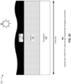
- Fig. 1A illustrates a side view of an example configuration of the optical filter 102.
- the first mirror 104 may have a first uniform thickness 110 along a first axis (e.g., a horizontal axis as shown in Fig. 1A ) of the optical filter 102 and the second mirror 106 may have a second uniform thickness 112 along the first axis.
- the first uniform thickness 110 may vary by less than a first mirror thickness threshold along the first axis.
- the first mirror thickness threshold may be less than or equal to 1%, 2%, and/or 3% of a maximum thickness of the first uniform thickness 110, of a minimum thickness of the first uniform thickness 110, and/or of an average thickness of the first uniform thickness 110 (e.g., along some or all of the first axis), among other examples.
- the second uniform thickness 112 may vary by less than a second mirror thickness threshold along the first axis.
- the second mirror thickness threshold may be less than or equal to 1%, 2%, and/or 3% of a maximum thickness of the second uniform thickness 112, of a minimum thickness of second uniform thickness 112, and/or of an average thickness of second uniform thickness 112 (e.g., along some or all of the first axis), among other examples.
- the spacer 108 may have a variable thickness 114 along the first axis.
- the variable thickness 114 may vary by more than, or a same amount as, a spacer thickness threshold along the first axis.
- the spacer thickness threshold may be less than or equal to 1%, 2%, and/or 3% of a maximum thickness of the variable thickness 114, of a minimum thickness of the variable thickness 114, and/or of an average thickness of the variable thickness 114 (e.g., along some or all of the first axis), among other examples.
- a spacer thickness threshold may be less than or equal to 1%, 2%, and/or 3% of a maximum thickness of the variable thickness 114, of a minimum thickness of the variable thickness 114, and/or of an average thickness of the variable thickness 114 (e.g., along some or all of the first axis), among other examples.
- the spacer 108 may have a first variable thickness 114-1 at a first position (e.g., a first end position associated with a minimum thickness of the variable thickness 114) along the first axis, and a second variable thickness 114-2 at a second position (e.g., a second end position associated with a maximum thickness of the variable thickness 114) along the first axis.
- the spacer 108 therefore has a variable thickness along the first axis when a difference between the first variable thickness 114-1 and the second variable thickness 114-2 is greater than or equal to the spacer thickness threshold.
- the spacer 108 may have a thickness profile (e.g., that is associated with the variable thickness 114) along the first axis of the optical filter 102.
- one or more portions of the thickness profile may have a non-linear slope (e.g., for each portion, of the one or more portions, a slope of a top surface of the spacer 108 may not be linear).
- the top surface of the spacer 108 has a curved surface (e.g., that can be described using a nonlinear function, not a linear function). Accordingly, any one portion of the thickness profile of the spacer 108 (as shown in Fig. 1A ) has a non-linear slope.
- one or more portions of the thickness profile may have a non-linear slope with an absolute value that is greater than zero.
- any one portion of the thickness profile of the spacer 108 may have a non-linear slope that does not include a sub-portion that is parallel to the first axis (e.g., the top surface of the spacer 108 does not include a horizontal sub-portion). Further description regarding thickness profiles is provided herein in relation to Figs. 2-3 .
- the optical filter 102 may include one or more blocking components (not shown in Fig. 1A ).
- the one or more blocking components may absorb, reflect, and/or or otherwise prevent light not associated with the plurality of spectral ranges (e.g., that the optical filter 102 is configured to pass) from passing through the optical filter 102.
- a blocking component may prevent passage, by the optical filter 102, of light with wavelengths that are not within the plurality of spectral ranges.
- the one or more blocking components may be disposed on at least one of the first mirror 104, the spacer 108, or the second mirror 106. For example, with reference to Fig.
- the one or more blocking components may be disposed on a bottom surface of the first mirror 104, a top surface of the first mirror 104 and/or a bottom surface of the spacer 108, a top surface of the spacer 108 and/or a bottom surface of the second mirror 106, and/or a top surface of the second mirror 106.
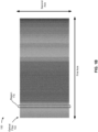
- Fig. 1B illustrates a top view of the optical filter 102.
- a second axis e.g., a vertical axis
- the first axis may be associated with a "length" of the optical filter 102 and the second axis may be associated with a "width" of the optical filter 102.
- the optical filter 102 may be configured to pass light associated with a spectral range, of the plurality of spectral ranges (e.g., that the optical filter 102 is configured to pass), across a region of the optical filter that is parallel to the second axis.
- the optical filter 102 may include a region 116 that is parallel to the second axis (e.g., the region 116 is a "width" region along a top surface of the optical filter 102 that is parallel to the second axis) and that is configured to pass light associated with a particular spectral range.
- a variation in center wavelength associated with the spectral range across the region may satisfy (e.g., be less than or equal to) a center wavelength variation threshold.
- the center wavelength variation threshold may be less than or equal to 1%, 2%, and/or 3% a width of the spectral range (e.g., a difference between a maximum of the spectral range and a minimum of the spectral range) and/or less than or equal to 1 nm, 2 nm, 3 nm, and/or another length.
- the optical filter 102 may have a reduced amount of optical smile.
- Fig. 1C illustrates a side view of an example optical sensor device 118 that includes the optical filter 102 and an optical sensor 120.
- the optical sensor 120 may be capable of sensing light.
- the optical sensor 120 may include an image sensor, a multispectral sensor, a spectral sensor, and/or similar sensor.
- the optical sensor 120 may include a silicon (Si) based sensor, an indium-gallium-arsenide (InGaAs) based sensor, a lead-sulfide (PbS) based sensor, or a germanium (Ge) based sensor, and may utilize one or more sensor technologies, such as a complementary metal-oxide-semiconductor (CMOS) technology, or a charge-coupled device (CCD) technology, among other examples.
- CMOS complementary metal-oxide-semiconductor
- CCD charge-coupled device
- the optical sensor 120 may include a front-side illumination (FSI) sensor, a back-side illumination (BSI) sensor, and/or another sensors.
- FSI front-side illumination
- BSI back-side illumination
- the optical sensor 120 may include a plurality of sensor elements 122.
- the plurality of sensor elements 122 may be arranged in a one-dimensional array, a two-dimensional array, and/or another arrangement on a surface of the optical sensor 120.
- the optical filter 102 may be configured to pass light associated with the plurality of spectral ranges to the plurality of sensor elements 122.
- a sensor element 122 may be configured to obtain information regarding light that falls incident on the sensor element 122 (e.g., after passing through a portion of the optical filter 102).
- a sensor element 122 may provide an indication of intensity of light that falls incident on the sensor element 122 (e.g., active/inactive, or a more granular indication of intensity).
- the optical sensor 120 may be configured to collect the information obtained by the one or more sensor elements 122 to generate sensor data.
- the optical filter 102 may be disposed over the optical sensor 120 in the optical sensor device 118.
- the optical filter 102 may be directly disposed on the optical sensor 120 or may be separated from the optical sensor 120 by a gap (e.g., a free space gap).
- Fig. 1D illustrates a side view of another example configuration of the optical filter 102, wherein the optical filter 102 includes the first mirror 104, the second mirror 106, and the spacer 108 (e.g., as described herein in relation to Figs. 1A-1C ), along with an additional spacer 124 and a third mirror 126.
- the additional spacer 124 may be positioned between the second mirror 106 and the third mirror 126.
- the additional spacer 124 may be disposed on the second mirror 106 (e.g., a bottom surface of the additional spacer 124 may disposed on a top surface of the second mirror 106) and the third mirror 126 may be disposed on the additional spacer 124 (e.g., a bottom surface of the second mirror 106 may be disposed on a top surface of the additional spacer 124).
- the additional spacer 124 may be configured in a same, or similar manner, as the spacer 108.
- the additional spacer 124 may comprise one or more materials, such as at least one of an Si material, an Si:H material, an a-Si material, an SiN material, a Ge material, a Ge:H material, an SiGe material, an SiGe:H material, an SiC material, an SiC:H material, an Si02 material, a Ta 2 O 5 material, a Nb 2 O 5 material, a NbTiO x material, a Nb 2 TaO 5 material, a Ti02 material, an Al 2 O 3 material, a ZrO 2 material, an Y 2 O 3 material, an AlN material, or a Hf02 material, among other examples.
- the additional spacer 124 may be formed as a single spacer (e.g., rather than a spacer comprising discrete parts or layers). Additionally, or alternatively, the additional spacer 124 may have a uniform, or a substantially uniform, crystal lattice structure (e.g., the additional spacer 124 may not include any interfaces within the additional spacer 124). For example, the additional spacer 124 may be formed as a single spacer using an etching procedure (e.g., in coordination with a grayscale lithography procedure), in a similar manner as described herein in relation to Fig. 5D .
- an etching procedure e.g., in coordination with a grayscale lithography procedure
- the additional spacer 124 may be configured to be transparent for the plurality of spectral ranges (e.g., that the optical filter 102 is configured to pass).
- the additional spacer 124 may be configured to transmit greater than a threshold percentage of light that has a wavelength that is within the plurality of spectral ranges.
- the threshold percentage of light may be greater than or equal to 30%, 50%, 75%, 90%, 95%, and/or 99%, for example.
- the additional spacer 124 may have a variable thickness 128 along the first axis (e.g., the horizontal axis as shown in Fig. ID).
- the variable thickness 114 may vary by more than, or a same amount as, an additional spacer thickness threshold along the first axis.
- the additional spacer thickness threshold may be less than or equal to 1%, 2%, and/or 3% of a maximum thickness of the variable thickness 128, of a minimum thickness of the variable thickness 128, and/or of an average thickness of the variable thickness 128 (e.g., along some or all of the first axis), among other examples.
- a maximum thickness of the variable thickness 128, of a minimum thickness of the variable thickness 128, and/or of an average thickness of the variable thickness 128 e.g., along some or all of the first axis
- the additional spacer 124 may have a first variable thickness 128-1 at a first position (e.g., a first end position associated with a maximum thickness of the variable thickness 128) along the first axis and a second variable thickness 128-2 at a second position (e.g., a second end position associated with a minimum thickness of the variable thickness 128) along the first axis.
- the additional spacer 124 therefore has a variable thickness along the first axis when a difference between the first variable thickness 128-1 and the second variable thickness 128-2 is greater than or equal to the spacer thickness threshold.
- the additional spacer 124 may have a thickness profile (e.g., that is associated with the variable thickness 128) along the first axis of the optical filter 102.
- one or more portions of the thickness profile may have a non-linear slope (e.g., for each portion, of the one or more portions, a slope of a top surface of additional spacer 124 may not be linear).
- the top surface of additional spacer 124 has a curved surface (e.g., that can be described using an exponential function, not a linear function). Accordingly, any one portion of the thickness profile of the additional spacer 124 (as shown in Fig. ID) has a non-linear slope.
- the one or more portions of the thickness profile may have a non-linear slope with an absolute value that is greater than zero (e.g., for each portion, of the one or more portions, a slope of a top surface of additional spacer 124 is not parallel to the first axis). Further description regarding thickness profiles is provided herein in relation to Figs. 2-3 .
- the third mirror 126 may be configured in a same, or similar manner, as the first mirror 104 and/or the second mirror 106.
- the third mirror 126 may comprise one or more metals, one or more dielectric materials, and/or one or more semiconductor materials, among other examples.
- the third mirror 126 may be configured to reflect one or more spectral ranges of the plurality of spectral ranges.
- the third mirror 126 may be configured to reflect light associated with a same spectral range as that reflected by the first mirror 104 and/or the second mirror 106. Additionally, or alternatively, the third mirror 126 may be configured to reflect light associated with a different spectral range than that reflected by the first mirror 104 and/or the second mirror 106.
- the third mirror 162 may have a third uniform thickness 130 along the first axis (e.g., the horizontal axis as shown in Fig. 1D ) of the optical filter 102.
- the third uniform thickness 130 may vary by less than a third mirror thickness threshold along the first axis.
- the third mirror thickness threshold may be less than or equal to 1%, 2%, and/or 3% of a maximum thickness of the third uniform thickness 130, of a minimum thickness of the third uniform thickness 130, and/or of an average thickness of the third uniform thickness 130 (e.g., along some or all of the first axis), among other examples.
- FIGS. 1A-1D are provided as an example. Other examples may differ from what is described with regard to Figs. 1A-1D .
- Fig. 2 is a diagram of an example implementation 200 of an optical filter 202.
- the optical filter may include a first mirror 204, a second mirror 206, and a spacer 208.
- the first mirror 204, the second mirror 206, and the spacer 208 may be respectively configured in a same, or similar, manner as that of the first mirror 104, the second mirror 106, and the spacer 108 of the optical filter 102 described herein in relation to Figs. 1A-1D .
- the optical filter 202 may include one or more blocking components (not shown in Fig. 2 ) that are configured in a same, or similar manner, as that of the one or more blocking components described herein in relation to Figs. 1A-1D .
- Fig. 2 illustrates a side view of an example configuration of the optical filter 202.
- the first mirror 204 may have a first uniform thickness 210 along a first axis (e.g., a horizontal axis as shown in Fig. 2 ) of the optical filter 202 and the second mirror 206 may have a second uniform thickness 212 along the first axis.
- the first uniform thickness 210 may vary by less than a first mirror thickness threshold along the first axis.
- the first mirror thickness threshold may be less than or equal to 1%, 2%, and/or 3% of a maximum thickness of the first uniform thickness 210, of a minimum thickness of the first uniform thickness 210, and/or of an average thickness of the first uniform thickness 210 (e.g., along some or all of the first axis), among other examples.
- the second uniform thickness 212 may vary by less than a second mirror thickness threshold along the first axis.
- the second mirror thickness threshold may be less than or equal to 1%, 2%, and/or 3% of a maximum thickness of the second uniform thickness 212, of a minimum thickness of second uniform thickness 212, and/or of an average thickness of second uniform thickness 212 (e.g., along some or all of the first axis), among other examples.
- the spacer 208 may have a variable thickness 214 along the first axis.
- the variable thickness 214 may vary by more than, or a same amount as, a spacer thickness threshold along the first axis.
- the spacer thickness threshold may be less than or equal to 1%, 2%, and/or 3% of a maximum thickness of the variable thickness 214, of a minimum thickness of the variable thickness 214, and/or of an average thickness of the variable thickness 214 (e.g., along some or all of the first axis), among other examples.
- a spacer thickness threshold may be less than or equal to 1%, 2%, and/or 3% of a maximum thickness of the variable thickness 214, of a minimum thickness of the variable thickness 214, and/or of an average thickness of the variable thickness 214 (e.g., along some or all of the first axis), among other examples.
- the spacer 208 may have a first variable thickness 214-1 at a first position (e.g., a first end position associated with a minimum thickness of the variable thickness 214) along the first axis and a second variable thickness 214-2 at a second position (e.g., a second end position associated with a maximum thickness of the variable thickness 214) along the first axis.
- the spacer 208 therefore has a variable thickness along the first axis when a difference between the first variable thickness 214-1 and the second variable thickness 214-2 is greater than or equal to the spacer thickness threshold.
- the spacer 208 may have a thickness profile (e.g., that is associated with the variable thickness 214) along the first axis of the optical filter 202.
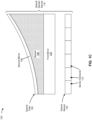
- one or more portions 216 of the thickness profile may have a non-linear slope (e.g., for each portion, of the one or more portions, a slope of a top surface of the spacer 208 may not be linear). For example, as shown in Fig.
- a portion of the top surface of the spacer 208 associated with a thickness profile portion 216-1 of the thickness profile has a linear slope (e.g., that can be described using a linear function) and another portion of the top surface of the spacer 208 associated with a thickness profile portion 216-2 of the thickness profile has a non-linear slope (e.g., that can be described using one or more exponential functions, not linear functions).
- the thickness profile portion 216-2 has a non-linear slope with an absolute value that is greater than zero (e.g., a top surface of the spacer 208 does not include a horizontal sub-portion).
- Fig. 2 is provided as an example. Other examples may differ from what is described with regard to Fig. 2 .
- Fig. 3 is a diagram of an example implementation 300 of an optical filter 302.
- the optical filter may include a first mirror 304, a second mirror 306, and a spacer 308.
- the first mirror 304, the second mirror 306, and the spacer 308 may be respectively configured in a same, or similar, manner as that of the first mirror 104, the second mirror 106, and the spacer 108 of the optical filter 102 described herein in relation to Figs. 1A-1D .
- the optical filter 302 may include one or more blocking components (not shown in Fig. 3 ) that are configured in a same, or similar manner, as that of the one or more blocking components described herein in relation to Figs. 1A-1D .
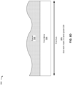
- Fig. 3 illustrates a side view of an example configuration of the optical filter 302.
- the first mirror 304 may have a first uniform thickness 310 along a first axis (e.g., a horizontal axis as shown in Fig. 3 ) of the optical filter 302 and the second mirror 306 may have a second uniform thickness 312 along the first axis.
- the first uniform thickness 310 may vary by less than a first mirror thickness threshold along the first axis.
- the first mirror thickness threshold may be less than or equal to 1%, 2%, and/or 3% of a maximum thickness of the first uniform thickness 310, of a minimum thickness of the first uniform thickness 310, and/or of an average thickness of the first uniform thickness 310 (e.g., along some or all of the first axis), among other examples.
- the second uniform thickness 312 may vary by less than a second mirror thickness threshold along the first axis.
- the second mirror thickness threshold may be less than or equal to 1%, 2%, and/or 3% of a maximum thickness of the second uniform thickness 312, of a minimum thickness of second uniform thickness 312, and/or of an average thickness of second uniform thickness 312 (e.g., along some or all of the first axis), among other examples.
- the spacer 308 may have a variable thickness 314 along the first axis.
- the variable thickness 314 may vary by more than, or a same amount as, a spacer thickness threshold along the first axis.
- the spacer thickness threshold may be less than or equal to 1%, 2%, and/or 3% of a maximum thickness of the variable thickness 314, of a minimum thickness of the variable thickness 314, and/or of an average thickness of the variable thickness 314 (e.g., along some or all of the first axis), among other examples.
- a spacer thickness threshold may be less than or equal to 1%, 2%, and/or 3% of a maximum thickness of the variable thickness 314, of a minimum thickness of the variable thickness 314, and/or of an average thickness of the variable thickness 314 (e.g., along some or all of the first axis), among other examples.
- the spacer 308 may have a first variable thickness 314-1 at a first position (e.g., a first end position associated with a minimum thickness of the variable thickness 314) along the first axis and a second variable thickness 314-2 at a second position (e.g., a middle position associated with a maximum thickness of the variable thickness 314) along the first axis.
- the spacer 308 therefore has a variable thickness along the first axis when a difference between the first variable thickness 314-1 and the second variable thickness 314-2 is greater than or equal to the spacer thickness threshold.
- the spacer 308 may have a thickness profile (e.g., that is associated with the variable thickness 314) along the first axis of the optical filter 302.
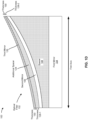
- one or more portions 316 of the thickness profile may have a non-linear slope (e.g., for each portion, of the one or more portions, a slope of a top surface of the spacer 308 may not be linear).
- the one or more portions 316 of the thickness profile may have a non-linear slope with an absolute value that is greater than zero (e.g., a top surface of the spacer 308 is not horizontal). For example, as shown in Fig.
- a first portion of the top surface of the spacer 308 associated with a thickness profile portion 316-1 of the thickness profile has a linear slope (e.g., that can be described using a linear function); a second portion of the top surface of the spacer 308 associated with a thickness profile portion 316-2 of the thickness profile has a non-linear slope (e.g., that can be described using one or more exponential functions, not linear functions) with an absolute value that is greater than zero (e.g., that is not horizontal); a third portion of the top surface of the spacer 308 associated with a thickness profile portion 316-3 of the thickness profile has a non-linear slope, but with an absolute value that is equal to zero (e.g., a portion of the top surface of the spacer 308 is horizontal); a fourth portion of the top surface of the spacer 308 associated with a thickness profile portion 316-4 of the thickness profile has a non-linear slope with an absolute value that is greater than zero; a fifth portion of the top surface of the spacer 308
- Fig. 3 is provided as an example. Other examples may differ from what is described with regard to Fig. 3 .
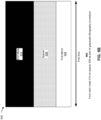
- Fig. 4 is a diagram of an example implementation 400 of a wafer 402.
- the wafer 402 may include a silicon (Si) wafer, a gallium arsenide (GaAs) wafer, an indium phosphide (InP) wafer, a germanium (Ge) wafer, and/or another type of wafer.
- a plurality of optical filters 404 may be disposed on the wafer 402 (e.g., formed on the wafer 402 using a formation process described herein in relation to Figs. 5A-5E ).
- each of the plurality of optical filters 404 may be configured in a same, or similar, manner as that of the optical filters 102, 202, and 302 described herein in relation to Figs. 1A-1D , 2 , and 3 .
- each optical filter 404, of the plurality of optical filters 404 may include a first mirror (e.g., that has a first uniform thickness), a second mirror (e.g., that has a second uniform thickness), and a spacer that is positioned between the first mirror and the second mirror.
- the spacer may have a variable thickness along a first axis of the optical filter, and/or a thickness profile of the spacer, along the first axis, may include one or more portions that have a non-linear slope (e.g., a non-linear slope with an absolute value greater than zero, as described elsewhere herein).
- each optical filter 404 may be configured to provide a matching spectral filtering performance (e.g., the plurality of optical filters 404 may each pass light associated with a same plurality of spectral ranges, and corresponding portions of the plurality of optical filters 404 may pass light associated with a same particular spectral range of the plurality of spectral ranges).
- each optical filter 404 may include a region that is parallel to a second axis of the optical filter 404 (e.g., like a region 116 of the optical filter 102, as shown in Fig. 1B ), wherein the second axis is orthogonal to the first axis of the optical filter 404.
- the region of the optical filter may be configured to pass light associated with a spectral range (e.g., of the plurality of spectral ranges), and a variation in center wavelength associated with the spectral range across the region may satisfy (e.g., be less than or equal to) a center wavelength variation threshold (e.g., as described elsewhere herein). Accordingly, the region may provide a consistent spectral performance across the region (e.g., one or more portions of the region may each pass light associated with the spectral range with a substantially same center wavelength).
- the plurality of optical filters 404 may be disposed on the wafer 402 to utilize an optimal amount of a surface area of the wafer 402. Accordingly, a particular number of optical filters 404 may be formed on the wafer 402 (e.g., using the formation process described herein in relation to Figs. 5A-5E ), such as to optimally utilize the surface area of the wafer.
- the particular number may be greater than or equal to 2 ⁇ R w , where R is a radius of the wafer 402 and w is a width of each optical filter 404 (e.g., along the second axis of the optical filter 404).
- Fig. 4 is provided as an example. Other examples may differ from what is described with regard to Fig. 4 .
- Figs. 5A-5E are diagrams of an example implementation 500 of a formation process for manufacturing an optical filter 502 (e.g., an optical filter that is the same as, or similar to, the optical filters 102, 202, 302, and/or 404, described herein in relation to Figs. 1A-1D , and 2-4 ).
- the optical filter 502 may be formed by forming a first mirror 504 (e.g., that is the same as, or similar to, the first mirror 104, the first mirror 204, and/or the first mirror 304 described herein in relation to Figs.
- a spacer 508 e.g., that is the same as, or similar to, the spacer 108, the spacer 208, and/or the spacer 308 described herein in relation to Figs. 1A-1D , 2 , and 3
- a second mirror 506 e.g., that is the same as, or similar to, the second mirror 106, the second mirror 206, and/or the second mirror 306 described herein in relation to Figs. 1A-1D , 2 , and 3 ).
- one or more layers and/or structures may be fabricated using a sputtering procedure, a photolithographic procedure, a grayscale lithographic procedure, an etching procedure, a lift off procedure, a scraping procedure, an annealing procedure, a molding procedure, a casting procedure, a machining procedure, and/or a stamping procedure, among other examples.
- the formation process may include forming the first mirror 504.
- the formation process may include forming the first mirror 504 on a region of a wafer (not shown in Fig. 5A ) (e.g., a region of the wafer 402).
- the first mirror 504 may be formed with a uniform thickness along a first axis of the optical filter 502 (e.g., the uniform thickness of the first mirror 504 may vary by less than a first mirror thickness threshold along the first axis, as described elsewhere herein).
- the formation process may include forming the spacer 508 on the first mirror 504.
- the formation process may include forming the spacer 508 on a top surface of the first mirror 504.
- the spacer 508 may be formed with a uniform thickness along the first axis (e.g., the uniform thickness of the spacer 508 may vary by less than a spacer thickness threshold along the first axis).
- the formation process may include forming an etch mask 510 on the spacer 508.
- the etch mask 510 may comprise a photo-sensitive material, such as a photo-sensitive polymer.
- the etch mask 510 may be formed using a grayscale lithography procedure, such as a grayscale electron beam lithography procedure or a grayscale photolithography procedure.
- the formation process may include depositing the etch mask 510 on the spacer 508.
- the formation process may further include exposing the etch mask 510 to different amounts of light (e.g., UV light) to the etch mask 510 to have a variable thickness along the first axis.
- the variable thickness of the etch mask 510 may vary by more than, or a same amount as, an etch mask thickness threshold along the first axis.
- the etch mask thickness threshold may be less than or equal to 1%, 2%, and/or 3% of a maximum thickness of the variable thickness of the etch mask 510 (e.g., after exposure to the different amounts of light), of a minimum thickness of the variable thickness of the etch mask 510, and/or of an average thickness of the variable thickness of the etch mask 510 (e.g., along some or all of the first axis), among other examples.
- the formation process may include etching the etch mask 510 and/or the spacer 508 using an etching procedure.
- the formation process may include using a single etching procedure, such as a single reactive ion etching procedure, to etch the etch mask 510 and/or the spacer 508.
- etching the etch mask 510 may eliminate the etch mask 510 (e.g., none, or substantially none, of the etch mask 510 remains after completion of the etching procedure).
- etching the spacer 508 may cause the spacer 508 to have a variable thickness along the first axis of the optical filter 502.
- the variable thickness of the spacer 508 may vary by more than, or a same amount as, a spacer thickness threshold (e.g., as described elsewhere herein) along the first axis.
- etching the spacer 508 may cause a region that is parallel to a second axis of the optical filter 502 (e.g., that is orthogonal to the first axis of the optical filter 502) of the spacer 508 to have a uniform thickness along the second axis.
- the uniform thickness of the region of the spacer 508 may vary by less than another spacer thickness threshold along the second axis (e.g., a variation in thickness across the region of the spacer 508 may satisfy the other spacer thickness threshold).
- the other spacer thickness threshold may be less than or equal to 1%, 2%, and/or 3% of a maximum thickness of the uniform thickness of the region of the spacer 508, of a minimum thickness of the uniform thickness of the region of the spacer 508, and/or of an average thickness of the uniform thickness of the region of the spacer 508 (e.g., along some or all of the second axis), among other examples.
- etching the spacer 508 may cause a thickness profile of the spacer 508, along the first axis, to have one or more portions that have a non-linear slope (e.g., a non-linear slope with an absolute value greater than zero, as described elsewhere herein).
- a non-linear slope e.g., a non-linear slope with an absolute value greater than zero, as described elsewhere herein.
- variable thickness of the spacer 508 along the first axis, the uniform thickness of the region of the spacer 508 along the second axis, and/or the non-linear slopes of the one or more portions of the thickness profile of the spacer 508 along the first axis may be respectively related to the variable thickness of the etch mask 510 along the first axis, a uniform thickness of the region of the etch mask 510 along the second axis, and/or non-linear slopes of one or more portions of a thickness profile of the etch mask 510 along the first axis (e.g., after exposing the etch mask 510 to light and prior to elimination of the etch mask 510 via the etching procedure).
- a thickness of a particular portion of the spacer 508 (e.g., after completion of the etching procedure) along an axis (e.g., the first axis or the second axis) may be a particular percentage of a thickness, along the axis, of a particular portion of the etch mask 510 that is disposed on the particular portion of the spacer 508 (e.g., after exposing the etch mask 510 to light and prior to elimination of the etch mask 510 via the etching procedure).
- a non-linear slope of a portion of the thickness profile of the spacer 508 along the first axis is directly related to a non-linear slope of a portion of the thickness profile of the etch mask 510 along the first axis (e.g., after exposing the etch mask 510 to light and prior to elimination of the etch mask 510 via the etching procedure).
- the formation process may include forming the second mirror 506 on the spacer 508.
- the formation process may include forming the second mirror 506 on a top surface of the spacer 508.
- the second mirror 506 may be formed with a uniform thickness along the first axis (e.g., the uniform thickness of the second mirror 506 may vary by less than a second mirror thickness threshold along the first axis, as described elsewhere herein).
- the formation process may include forming an additional spacer (e.g., the additional spacer 124, as described herein in relation to Fig. ID) on the second mirror 506 and an additional etch mask on the additional spacer (e.g., in a similar manner as that described herein in relation to Figs. 5A-5B ).
- the formation process may include etching the additional etch mask and/or the additional spacer using the etching procedure (e.g., in a similar manner as that described herein in relation to Figs. 5C-5D ).
- etching the additional etch mask may eliminate the additional etch mask, may cause the additional spacer to have a variable thickness along the first axis of the optical filter 502 (e.g., as shown by the variable thickness 128 of the additional spacer 124 shown in Fig. ID), and/or may cause a thickness profile of the additional spacer, along the first axis, to include one or more portions that have a non-linear slope (e.g., a non-linear slope with an absolute value greater than zero, as shown by the non-linear slope of the thickness profile of the additional spacer 124 shown in Fig. ID).
- the formation process may include forming a third mirror (e.g., the third mirror 126, as described herein in relation to Fig. ID) on the additional spacer (e.g., in a similar manner as that described herein in relation to Fig. 5E ).
- the formation process may include forming a plurality of optical filters 502 on a wafer (e.g., on respective regions of the wafer) at a same time (e.g., as part of the same formation process). Accordingly, each optical filter 502 may be configured to provide a matching spectral filter performance (e.g., as other optical filters 502 of the plurality of optical filters 502), as described elsewhere herein.
- FIGS. 5A-5E are provided as an example. Other examples may differ from what is described with regard to Figs. 5A-5E .
- satisfying a threshold may, depending on the context, refer to a value being greater than the threshold, greater than or equal to the threshold, less than the threshold, less than or equal to the threshold, equal to the threshold, not equal to the threshold, or the like.
- a, b, or c is intended to cover a, b, c, a-b, a-c, b-c, and a-b-c, as well as any combination with multiple of the same item.
- the terms “has,” “have,” “having,” or the like are intended to be open-ended terms. Further, the phrase “based on” is intended to mean “based, at least in part, on” unless explicitly stated otherwise. Also, as used herein, the term “or” is intended to be inclusive when used in a series and may be used interchangeably with “and/or,” unless explicitly stated otherwise (e.g., if used in combination with “either” or “only one of”). Further, spatially relative terms, such as “below,” “lower,” “bottom,” “above,” “upper,” “top,” and the like, may be used herein for ease of description to describe one element or feature's relationship to another element(s) or feature(s) as illustrated in the figures.
- the spatially relative terms are intended to encompass different orientations of the apparatus, device, and/or element in use or operation in addition to the orientation depicted in the figures.
- the apparatus may be otherwise oriented (rotated 90 degrees or at other orientations) and the spatially relative descriptors used herein may likewise be interpreted accordingly.
Landscapes
- Physics & Mathematics (AREA)
- General Physics & Mathematics (AREA)
- Optics & Photonics (AREA)
- Spectroscopy & Molecular Physics (AREA)
- Health & Medical Sciences (AREA)
- Toxicology (AREA)
- Optical Filters (AREA)
Abstract
Description
- An optical sensor device may be utilized to capture information. For example, the optical sensor device may capture information relating to a set of electromagnetic frequencies. The optical sensor device may include a set of sensor elements (e.g., optical sensors, spectral sensors, and/or image sensors) that capture the information. For example, an array of sensor elements may be utilized to capture information relating to multiple frequencies. The sensor element array may be associated with an optical filter. The optical filter may include one or more channels that respectively pass particular frequencies to sensor elements of the sensor element array.
- In some implementations, an optical filter includes a first mirror that has a first uniform thickness; a second mirror that has a second uniform thickness; and a spacer that is positioned between the first mirror and the second mirror, wherein the spacer has a variable thickness along a first axis of the optical filter and a thickness profile of the spacer, along the first axis, includes one or more portions that have a non-linear slope with an absolute value that is greater than zero.
- A second axis of the optical filter may be orthogonal to the first axis, wherein: the optical filter may be configured to pass light associated with a spectral range across a region of the optical filter that is parallel to the second axis; and a variation in center wavelength associated with the spectral range across the region may satisfy a center wavelength variation threshold.
- A variation in thickness across a region of the spacer that is parallel to the second axis may satisfy a spacer thickness threshold.
- The optical filter may be configured to pass light associated with a plurality of spectral ranges that comprises at least one of: one or more portions of an ultraviolet light spectral range, one or more portions of a visible light spectral range, one or more portions of a near-infrared light spectral range, one or more portions of a short-wave infrared light spectral range, one or more portions of a mid-wave infrared light spectral range; or one or more portions of a long-wave infrared light spectral range.
- The optical filter may be configured to pass light associated with a plurality of spectral ranges, and wherein the spacer may be configured to transmit greater than a threshold percentage of light associated with a spectral range that is within the plurality of spectral ranges.
- The spacer may be formed using an etching procedure.
- The optical filter may further comprise: a third mirror that has a third uniform thickness; and an additional spacer that is positioned between the third mirror and one of the first mirror and the second mirror, wherein the additional spacer may have a variable thickness along the first axis of the optical filter.
- A thickness profile of the additional spacer, along the first axis, may include one or more portions that have a non-linear slope with an absolute value that is greater than zero.
- The optical filter may further comprise: one or more blocking components disposed on a surface of at least one of the first mirror, the second mirror, or the spacer.
- In some implementations, a wafer includes a plurality of optical filters, wherein each optical filter includes: a first mirror that has a first uniform thickness; a second mirror that has a second uniform thickness; and a spacer that is positioned between the first mirror and the second mirror, wherein at least one of: the spacer has a variable thickness along a first axis of the optical filter, or a thickness profile of the spacer, along the first axis, includes one or more portions that have a non-linear slope with an absolute value that is greater than zero.
- For each optical filter, of the plurality of optical filters, a second axis of the optical filter may be orthogonal to the first axis, wherein: the optical filter may be configured to pass light associated with a spectral range across a region of the optical filter that is parallel to the second axis; and a variation in center wavelength associated with the spectral range across the region may satisfy a center wavelength variation threshold.
- The wafer may have a radius R and each of the plurality of optical filters may have a width w, and wherein a number of the plurality of optical filters may be greater than or equal to

- Each optical filter, of the plurality of optical filters, may be configured to provide a matching spectral filtering performance.
- Each optical filter, of the plurality of optical filters, may further comprise: a third mirror that may have a third uniform thickness; and an additional spacer that may be positioned between the third mirror and one of the first mirror and the second mirror, wherein at least one of: the additional spacer may have a variable thickness along the first axis of the optical filter, or a thickness profile of the additional spacer, along the first axis, may include one or more portions that have a non-linear slope with an absolute value that is greater than zero.
- Each optical filter, of the plurality of optical filters, may further comprise: one or more blocking components disposed on a surface of at least one of the first mirror or the second mirror.
- In some implementations, a method of manufacturing a plurality of optical filters comprises, for each optical filter: forming, on a region of a wafer, a first mirror; forming, on the first mirror, a spacer; forming an etch mask on the spacer; etching the etch mask and the spacer, wherein etching the etch mask eliminates the etch mask and etching the spacer causes the spacer to have a variable thickness along a first axis of the optical filter and a thickness profile of the spacer, along the first axis, to include one or more portions that have a non-linear slope with an absolute value that is greater than zero; and forming, on the spacer, a second mirror.
- The etch mask may be formed using a grayscale lithography procedure.
- A second axis of the optical filter may be orthogonal to the first axis, and etching the spacer may further cause a variation in thickness across a region of the spacer that is parallel to the second axis to satisfy a spacer thickness threshold.
- The etch mask and the spacer may be etched using a single etching procedure.
- The method may further comprise, for each optical filter: forming, on the second mirror, an additional spacer; forming an additional etch mask on the additional spacer; etching the additional etch mask and the additional spacer, wherein: etching the additional etch mask may eliminate the additional etch mask, and etching the additional spacer may cause the additional spacer to have a variable thickness along the first axis of the optical filter; and forming, on the additional spacer, a third mirror.
-
-
Figs. 1A-1D are diagrams of an example implementation described herein. -
Fig. 2 is a diagram of an example implementation of an optical filter described herein. -
Fig. 3 is a diagram of an example implementation of an optical filter described herein. -
Fig. 4 is a diagram of an example implementation of a wafer described herein. -
Figs. 5A-5E are diagrams of an example implementation of a formation process for manufacturing an optical filter described herein. - The following detailed description of example implementations refers to the accompanying drawings. The same reference numbers in different drawings may identify the same or similar elements. The following description uses a spectrometer as an example. However, the techniques, principles, procedures, and methods described herein may be used with any sensor, including but not limited to other optical sensors and spectral sensors.
- A continuously variable filter (CVF) typically includes a first mirror with a variable thickness in a first direction of the CVF (e.g., a length of the CVF), a second mirror with a variable thickness in the first direction of the CVF, and a spacer with a variable thickness in the first direction of the CVF that is disposed between the first mirror and the second mirror. For example, the CVF may be "wedge-shaped," wherein respective thickness profiles of the first mirror, the second mirror, and the spacer have a linear slope (e.g., respective top surfaces of the first mirror, the second mirror, and the spacer can be described using one or more linear functions). In this way, when the CVF passes light associated with a plurality of spectral ranges, different regions (e.g., regions parallel to a second direction, a width, of the CVF) may pass respective spectral ranges of the plurality of spectral ranges.
- In many cases, a CVF is formed using one or more physical deposition processes. However, such processes have limitations. For example, it is difficult to form mirrors with uniform thicknesses and to form a spacer with a thickness profile that has a non-linear slope. Consequently, forming a CVF to provide a particular spectral filtering performance (e.g., that requires mirrors with uniform thicknesses and/or a spacer with a thickness profile that has a non-linear slope) is not possible using the one or more physical deposition processes.
- Further, the one or more physical deposition processes typically require multiple CVFs to be formed at a same time in an annular arrangement on a wafer (e.g., a circular wafer). Accordingly, after formation, each CVF has to be cut to have a particular shape (e.g., a rectilinear shape) and the CVFs have to further be compared to each other and processed to ensure that the CVFs provide a matching spectral filtering performance (e.g., across each of the CVFs). Further, forming the CVFs in the annular arrangement often results in a significant amount of a surface area of the wafer not being utilized to form CVFs and/or being deposited with material that ultimately will not be included in the CVFs (e.g., that will be cut and discarded to cause the CVFs to have rectilinear shapes).
- Additionally, forming the CVFs in the annular arrangement results in each CVF having an "optical smile," wherein a region of the CVF (e.g., across a width of the CVF, in the second direction of the CVF) that is configured to pass a particular spectral range has significant variation in center wavelength associated with the spectral range across the region (e.g., different portions of the region pass light with different center wavelengths that are within the spectral range). In some cases, the variation can be defined as

- Some implementations described herein provide an optical filter. The optical filter includes a first mirror and a second mirror with respectively uniform thicknesses. The optical filter includes a spacer positioned between the first mirror and the second mirror, wherein the spacer has a variable thickness along a first axis of the optical filter (e.g., a length of the optical filter). Accordingly, the optical filter provides a spectral filtering performance (e.g., that requires mirrors with uniform thicknesses) that cannot be provided using a typical CVF (e.g., that is formed using conventional deposition processes). In some implementations, a thickness profile of the spacer, along the first axis, includes one or more portions that have a non-linear slope (e.g., with an absolute value that is greater than zero). In this way, the optical filter further provides a spectral filtering performance (e.g., that requires a thickness profile of the spacer that has a non-linear slope) that is not possible to be provided using the typical CVF.
- Some implementations described herein provide a formation process for manufacturing the optical filter that includes using a sputtering procedure to create the first mirror and the second mirror, which enables the first mirror and the second mirror to have uniform thicknesses. Further, the formation process includes using a grayscale lithography procedure to form the spacer, which enables the thickness profile of the spacer, along the first axis, to include one or more portions that have a non-linear slope. The grayscale lithography procedure also enables the spacer to have a uniform thickness along the second axis, which reduces respective variations in center wavelength across regions of the optical filter that are parallel to the second axis of the optical filter (e.g., across width regions of the optical filter). This therefore minimizes an amount of optical smile associated with the optical filter, which improves a performance of the optical filter (e.g., a finesse, a selectivity, and/or other characteristics of the optical filter) as compared to a typical CVF. This allows the optical filter to be used in applications in which a typical CVF could not otherwise be used (e.g., applications that require a consistent performance across the width of the optical filter).
- In some implementations, the formation process may be used to form a plurality of optical filters on a wafer (e.g., on respective regions of the wafer). The formation process enables each optical filter to be formed to have a particular shape (e.g., a rectilinear shape), without needing additional processing to resize the optical filter and match a spectral filtering performance of the optical filter with that of other optical filters formed on the wafer. Further, the formation process enables the plurality of optical filters to be formed in a non-annular arrangement on the wafer, which allows for an increased amount of a surface area of the wafer to be utilized to form CVFs and/or for a reduced amount of material that is discarded to form CVFs (e.g., as compared to conventional physical deposition processes).
-
Figs. 1A-1D are diagram of anexample implementation 100 described herein. As shown inFigs. 1A-1D , theexample implementation 100 may include anoptical filter 102, such as for an optical sensor device (e.g., anoptical sensor device 118, described herein). The optical sensor device may be a spectrometer device that performs spectroscopy, such as vibrational spectroscopy, near-infrared (NIR) spectroscopy, mid-infrared spectroscopy (mid-IR), and/or Raman spectroscopy. - In some implementations, the
optical filter 102 may be configured to pass light associated with a plurality of spectral ranges of an electromagnetic spectrum (e.g., pass light with wavelengths that are within the plurality of spectral ranges). The plurality of spectral ranges may include, for example, one or more portions of an ultraviolet (UV) light spectral range (e.g., one or more portions of a spectral range within 100 to 379 nm), one or more portions of a visible light spectral range (e.g., one or more portions of a spectral range within 380 to 779 nm), one or more portions of an NIR light spectral range (e.g., one or more portions of a spectral range within 780 to 1399 nm), one or more portions of short-wave infrared (SWIR) light spectral range (e.g., one or more portions of a spectral range within 1400 to 2999 nm), one or more portions of a mid-wave infrared (MWIR) light spectral range (e.g., one or more portions of a spectral range within 3000 to 7999 nm), and/or one or more portions of a long-wave infrared (LWIR) light spectral range (e.g., one or more portions of a spectral range within 8000 nm to 15000 nm). - As further shown in
Figs. 1A-1D , the optical filter may include afirst mirror 104, asecond mirror 106, and aspacer 108. Thespacer 108 may be positioned between thefirst mirror 104 and thesecond mirror 106. For example, as further shown inFigs. 1A and1C-1D , thespacer 108 may be disposed on the first mirror 104 (e.g., a bottom surface of thespacer 108 may disposed on a top surface of the first mirror 104) and thesecond mirror 106 may be disposed on the spacer 108 (e.g., a bottom surface of thesecond mirror 106 may be disposed on top surface of the spacer 108). - Each mirror, of the
first mirror 104 and thesecond mirror 106, may comprise one or more metals, one or more dielectric materials, and/or one or more semiconductor materials, among other examples. Each mirror may be configured to reflect one or more spectral ranges of the plurality of spectral ranges (e.g., reflect light with a wavelength that is within the one or more spectral ranges). For example, each mirror may be configured to reflect one or more spectral ranges associated with the one or more portions of the UV light spectral range, the one or more portions of the visible light spectral range, the one or more portions of the NIR light spectral range, the one or more portions of the SWIR light spectral range, the one or more portions of the MWIR light spectral range, and/or the one or more portions of the LWIR light spectral range. In some implementations, thefirst mirror 104 and thesecond mirror 106 may each be configured to reflect light associated with a same spectral range of the plurality of spectral ranges. Additionally, or alternatively, thefirst mirror 104 may be configured to reflect light associated with a first spectral range of the plurality of spectral ranges and thesecond mirror 106 may be configured to reflect light associated with a second spectral range of the plurality of spectral ranges, where the second spectral range is different than the first spectral range (e.g., where at least a portion of the first spectral range does not overlap with the second spectral range, or vice versa). - The
spacer 108 may comprise one or more materials, such as at least one of a silicon (Si) material, a hydrogenated silicon (Si:H) material, an amorphous silicon (a-Si) material, a silicon nitride (SiN) material, a germanium (Ge) material, a hydrogenated germanium (Ge:H) material, a silicon germanium (SiGe) material, a hydrogenated silicon germanium (SiGe:H) material, a silicon carbide (SiC) material, a hydrogenated silicon carbide (SiC:H) material, a silicon dioxide (Si02) material, a tantalum pentoxide (Ta2O5) material, a niobium pentoxide (Nb2O5) material, a niobium titanium oxide (NbTiOx) material, a niobium tantalum pentoxide (Nb2TaO5) material, a titanium dioxide (Ti02) material, an aluminum oxide (Al2O3) material, a zirconium oxide (Zr02) material, an yttrium oxide (Y2O3) material, an aluminum nitride (AlN), or a hafnium oxide (Hf02) material, among other examples. Thespacer 108 may be formed as a single spacer (e.g., rather than a spacer comprising discrete parts or layers). Additionally, or alternatively, thespacer 108 may have a uniform, or a substantially uniform, crystal lattice structure (e.g., thespacer 108 may not include any interfaces within the spacer 108). For example, thespacer 108 may be formed as a single spacer using an etching procedure (e.g., in coordination with a grayscale lithography procedure), as further described herein in relation toFig. 5D . In some implementations, thespacer 108 may be configured to be transparent for the plurality of spectral ranges (e.g., that theoptical filter 102 is configured to pass). For example, thespacer 108 may be configured to transmit greater than a threshold percentage of light that has a wavelength that is within the plurality of spectral ranges. The threshold percentage of light may be greater than or equal to 30%, 50%, 75%, 90%, 95%, and/or 99%, for example. -
Fig. 1A illustrates a side view of an example configuration of theoptical filter 102. As shown inFig. 1A , thefirst mirror 104 may have afirst uniform thickness 110 along a first axis (e.g., a horizontal axis as shown inFig. 1A ) of theoptical filter 102 and thesecond mirror 106 may have asecond uniform thickness 112 along the first axis. For example, thefirst uniform thickness 110 may vary by less than a first mirror thickness threshold along the first axis. The first mirror thickness threshold may be less than or equal to 1%, 2%, and/or 3% of a maximum thickness of thefirst uniform thickness 110, of a minimum thickness of thefirst uniform thickness 110, and/or of an average thickness of the first uniform thickness 110 (e.g., along some or all of the first axis), among other examples. As another example, thesecond uniform thickness 112 may vary by less than a second mirror thickness threshold along the first axis. The second mirror thickness threshold may be less than or equal to 1%, 2%, and/or 3% of a maximum thickness of thesecond uniform thickness 112, of a minimum thickness of seconduniform thickness 112, and/or of an average thickness of second uniform thickness 112 (e.g., along some or all of the first axis), among other examples. - The
spacer 108 may have a variable thickness 114 along the first axis. For example, the variable thickness 114 may vary by more than, or a same amount as, a spacer thickness threshold along the first axis. The spacer thickness threshold may be less than or equal to 1%, 2%, and/or 3% of a maximum thickness of the variable thickness 114, of a minimum thickness of the variable thickness 114, and/or of an average thickness of the variable thickness 114 (e.g., along some or all of the first axis), among other examples. In a particular example, as further shown inFig. 1A , thespacer 108 may have a first variable thickness 114-1 at a first position (e.g., a first end position associated with a minimum thickness of the variable thickness 114) along the first axis, and a second variable thickness 114-2 at a second position (e.g., a second end position associated with a maximum thickness of the variable thickness 114) along the first axis. Thespacer 108 therefore has a variable thickness along the first axis when a difference between the first variable thickness 114-1 and the second variable thickness 114-2 is greater than or equal to the spacer thickness threshold. - The
spacer 108 may have a thickness profile (e.g., that is associated with the variable thickness 114) along the first axis of theoptical filter 102. In some implementations, one or more portions of the thickness profile may have a non-linear slope (e.g., for each portion, of the one or more portions, a slope of a top surface of thespacer 108 may not be linear). For example, as shown inFig. 1A , the top surface of thespacer 108 has a curved surface (e.g., that can be described using a nonlinear function, not a linear function). Accordingly, any one portion of the thickness profile of the spacer 108 (as shown inFig. 1A ) has a non-linear slope. Additionally, in some implementations, one or more portions of the thickness profile may have a non-linear slope with an absolute value that is greater than zero. For example, any one portion of the thickness profile of thespacer 108 may have a non-linear slope that does not include a sub-portion that is parallel to the first axis (e.g., the top surface of thespacer 108 does not include a horizontal sub-portion). Further description regarding thickness profiles is provided herein in relation toFigs. 2-3 . - In some implementations, the
optical filter 102 may include one or more blocking components (not shown inFig. 1A ). The one or more blocking components may absorb, reflect, and/or or otherwise prevent light not associated with the plurality of spectral ranges (e.g., that theoptical filter 102 is configured to pass) from passing through theoptical filter 102. For example, a blocking component may prevent passage, by theoptical filter 102, of light with wavelengths that are not within the plurality of spectral ranges. The one or more blocking components may be disposed on at least one of thefirst mirror 104, thespacer 108, or thesecond mirror 106. For example, with reference toFig. 1A , the one or more blocking components may be disposed on a bottom surface of thefirst mirror 104, a top surface of thefirst mirror 104 and/or a bottom surface of thespacer 108, a top surface of thespacer 108 and/or a bottom surface of thesecond mirror 106, and/or a top surface of thesecond mirror 106. -
Fig. 1B illustrates a top view of theoptical filter 102. As shown inFig. 1B , a second axis (e.g., a vertical axis) of theoptical filter 102 may be orthogonal to the first axis (e.g., the horizontal axis) of theoptical filter 102. The first axis may be associated with a "length" of theoptical filter 102 and the second axis may be associated with a "width" of theoptical filter 102. - The
optical filter 102 may be configured to pass light associated with a spectral range, of the plurality of spectral ranges (e.g., that theoptical filter 102 is configured to pass), across a region of the optical filter that is parallel to the second axis. For example, as further shown inFig. 1B , theoptical filter 102 may include aregion 116 that is parallel to the second axis (e.g., theregion 116 is a "width" region along a top surface of theoptical filter 102 that is parallel to the second axis) and that is configured to pass light associated with a particular spectral range. In some implementations, a variation in center wavelength associated with the spectral range across the region (e.g., at one or more positions across the region, as shown inFig. 1B ) may satisfy (e.g., be less than or equal to) a center wavelength variation threshold. The center wavelength variation threshold may be less than or equal to 1%, 2%, and/or 3% a width of the spectral range (e.g., a difference between a maximum of the spectral range and a minimum of the spectral range) and/or less than or equal to 1 nm, 2 nm, 3 nm, and/or another length. In this way, theoptical filter 102 may have a reduced amount of optical smile. -
Fig. 1C illustrates a side view of an exampleoptical sensor device 118 that includes theoptical filter 102 and anoptical sensor 120. Theoptical sensor 120 may be capable of sensing light. For example, theoptical sensor 120 may include an image sensor, a multispectral sensor, a spectral sensor, and/or similar sensor. In some implementations, theoptical sensor 120 may include a silicon (Si) based sensor, an indium-gallium-arsenide (InGaAs) based sensor, a lead-sulfide (PbS) based sensor, or a germanium (Ge) based sensor, and may utilize one or more sensor technologies, such as a complementary metal-oxide-semiconductor (CMOS) technology, or a charge-coupled device (CCD) technology, among other examples. In some implementations, theoptical sensor 120 may include a front-side illumination (FSI) sensor, a back-side illumination (BSI) sensor, and/or another sensors. - As further shown in
Fig. 1C , theoptical sensor 120 may include a plurality ofsensor elements 122. The plurality ofsensor elements 122 may be arranged in a one-dimensional array, a two-dimensional array, and/or another arrangement on a surface of theoptical sensor 120. In some implementations, theoptical filter 102 may be configured to pass light associated with the plurality of spectral ranges to the plurality ofsensor elements 122. Asensor element 122 may be configured to obtain information regarding light that falls incident on the sensor element 122 (e.g., after passing through a portion of the optical filter 102). For example, asensor element 122 may provide an indication of intensity of light that falls incident on the sensor element 122 (e.g., active/inactive, or a more granular indication of intensity). Theoptical sensor 120 may be configured to collect the information obtained by the one ormore sensor elements 122 to generate sensor data. - As further shown in
Fig. 1C , theoptical filter 102 may be disposed over theoptical sensor 120 in theoptical sensor device 118. Theoptical filter 102 may be directly disposed on theoptical sensor 120 or may be separated from theoptical sensor 120 by a gap (e.g., a free space gap). -
Fig. 1D illustrates a side view of another example configuration of theoptical filter 102, wherein theoptical filter 102 includes thefirst mirror 104, thesecond mirror 106, and the spacer 108 (e.g., as described herein in relation toFigs. 1A-1C ), along with anadditional spacer 124 and athird mirror 126. Theadditional spacer 124 may be positioned between thesecond mirror 106 and thethird mirror 126. For example, as further shown in Fig. ID, theadditional spacer 124 may be disposed on the second mirror 106 (e.g., a bottom surface of theadditional spacer 124 may disposed on a top surface of the second mirror 106) and thethird mirror 126 may be disposed on the additional spacer 124 (e.g., a bottom surface of thesecond mirror 106 may be disposed on a top surface of the additional spacer 124). - The
additional spacer 124 may be configured in a same, or similar manner, as thespacer 108. For example, theadditional spacer 124 may comprise one or more materials, such as at least one of an Si material, an Si:H material, an a-Si material, an SiN material, a Ge material, a Ge:H material, an SiGe material, an SiGe:H material, an SiC material, an SiC:H material, an Si02 material, a Ta2O5 material, a Nb2O5 material, a NbTiOx material, a Nb2TaO5 material, a Ti02 material, an Al2O3 material, a ZrO2 material, an Y2O3 material, an AlN material, or a Hf02 material, among other examples. Theadditional spacer 124 may be formed as a single spacer (e.g., rather than a spacer comprising discrete parts or layers). Additionally, or alternatively, theadditional spacer 124 may have a uniform, or a substantially uniform, crystal lattice structure (e.g., theadditional spacer 124 may not include any interfaces within the additional spacer 124). For example, theadditional spacer 124 may be formed as a single spacer using an etching procedure (e.g., in coordination with a grayscale lithography procedure), in a similar manner as described herein in relation toFig. 5D . In some implementations, theadditional spacer 124 may be configured to be transparent for the plurality of spectral ranges (e.g., that theoptical filter 102 is configured to pass). For example, theadditional spacer 124 may be configured to transmit greater than a threshold percentage of light that has a wavelength that is within the plurality of spectral ranges. The threshold percentage of light may be greater than or equal to 30%, 50%, 75%, 90%, 95%, and/or 99%, for example. - As further shown in Fig. ID, the
additional spacer 124 may have a variable thickness 128 along the first axis (e.g., the horizontal axis as shown in Fig. ID). For example, the variable thickness 114 may vary by more than, or a same amount as, an additional spacer thickness threshold along the first axis. The additional spacer thickness threshold may be less than or equal to 1%, 2%, and/or 3% of a maximum thickness of the variable thickness 128, of a minimum thickness of the variable thickness 128, and/or of an average thickness of the variable thickness 128 (e.g., along some or all of the first axis), among other examples. In a particular example, as further shown in Fig. ID, theadditional spacer 124 may have a first variable thickness 128-1 at a first position (e.g., a first end position associated with a maximum thickness of the variable thickness 128) along the first axis and a second variable thickness 128-2 at a second position (e.g., a second end position associated with a minimum thickness of the variable thickness 128) along the first axis. Theadditional spacer 124 therefore has a variable thickness along the first axis when a difference between the first variable thickness 128-1 and the second variable thickness 128-2 is greater than or equal to the spacer thickness threshold. - As further shown in Fig. ID, the
additional spacer 124 may have a thickness profile (e.g., that is associated with the variable thickness 128) along the first axis of theoptical filter 102. In some implementations, one or more portions of the thickness profile may have a non-linear slope (e.g., for each portion, of the one or more portions, a slope of a top surface ofadditional spacer 124 may not be linear). For example, as shown in Fig. ID, the top surface ofadditional spacer 124 has a curved surface (e.g., that can be described using an exponential function, not a linear function). Accordingly, any one portion of the thickness profile of the additional spacer 124 (as shown in Fig. ID) has a non-linear slope. As further shown in Fig. ID, the one or more portions of the thickness profile may have a non-linear slope with an absolute value that is greater than zero (e.g., for each portion, of the one or more portions, a slope of a top surface ofadditional spacer 124 is not parallel to the first axis). Further description regarding thickness profiles is provided herein in relation toFigs. 2-3 . - The
third mirror 126 may be configured in a same, or similar manner, as thefirst mirror 104 and/or thesecond mirror 106. For example, thethird mirror 126 may comprise one or more metals, one or more dielectric materials, and/or one or more semiconductor materials, among other examples. Thethird mirror 126 may be configured to reflect one or more spectral ranges of the plurality of spectral ranges. Thethird mirror 126 may be configured to reflect light associated with a same spectral range as that reflected by thefirst mirror 104 and/or thesecond mirror 106. Additionally, or alternatively, thethird mirror 126 may be configured to reflect light associated with a different spectral range than that reflected by thefirst mirror 104 and/or thesecond mirror 106. - As further shown in Fig. ID, the third mirror 162 may have a third
uniform thickness 130 along the first axis (e.g., the horizontal axis as shown inFig. 1D ) of theoptical filter 102. For example, the thirduniform thickness 130 may vary by less than a third mirror thickness threshold along the first axis. The third mirror thickness threshold may be less than or equal to 1%, 2%, and/or 3% of a maximum thickness of the thirduniform thickness 130, of a minimum thickness of the thirduniform thickness 130, and/or of an average thickness of the third uniform thickness 130 (e.g., along some or all of the first axis), among other examples. - As indicated above,
Figs. 1A-1D are provided as an example. Other examples may differ from what is described with regard toFigs. 1A-1D . -
Fig. 2 is a diagram of anexample implementation 200 of anoptical filter 202. As shown inFig. 2 , the optical filter may include afirst mirror 204, asecond mirror 206, and aspacer 208. Thefirst mirror 204, thesecond mirror 206, and thespacer 208 may be respectively configured in a same, or similar, manner as that of thefirst mirror 104, thesecond mirror 106, and thespacer 108 of theoptical filter 102 described herein in relation toFigs. 1A-1D . In some implementations, theoptical filter 202 may include one or more blocking components (not shown inFig. 2 ) that are configured in a same, or similar manner, as that of the one or more blocking components described herein in relation toFigs. 1A-1D . -
Fig. 2 illustrates a side view of an example configuration of theoptical filter 202. As shown inFig. 2 , thefirst mirror 204 may have afirst uniform thickness 210 along a first axis (e.g., a horizontal axis as shown inFig. 2 ) of theoptical filter 202 and thesecond mirror 206 may have asecond uniform thickness 212 along the first axis. For example, thefirst uniform thickness 210 may vary by less than a first mirror thickness threshold along the first axis. The first mirror thickness threshold may be less than or equal to 1%, 2%, and/or 3% of a maximum thickness of thefirst uniform thickness 210, of a minimum thickness of thefirst uniform thickness 210, and/or of an average thickness of the first uniform thickness 210 (e.g., along some or all of the first axis), among other examples. As another example, thesecond uniform thickness 212 may vary by less than a second mirror thickness threshold along the first axis. The second mirror thickness threshold may be less than or equal to 1%, 2%, and/or 3% of a maximum thickness of thesecond uniform thickness 212, of a minimum thickness of seconduniform thickness 212, and/or of an average thickness of second uniform thickness 212 (e.g., along some or all of the first axis), among other examples. - The
spacer 208 may have a variable thickness 214 along the first axis. For example, the variable thickness 214 may vary by more than, or a same amount as, a spacer thickness threshold along the first axis. The spacer thickness threshold may be less than or equal to 1%, 2%, and/or 3% of a maximum thickness of the variable thickness 214, of a minimum thickness of the variable thickness 214, and/or of an average thickness of the variable thickness 214 (e.g., along some or all of the first axis), among other examples. In a particular example, as further shown inFig. 2 , thespacer 208 may have a first variable thickness 214-1 at a first position (e.g., a first end position associated with a minimum thickness of the variable thickness 214) along the first axis and a second variable thickness 214-2 at a second position (e.g., a second end position associated with a maximum thickness of the variable thickness 214) along the first axis. Thespacer 208 therefore has a variable thickness along the first axis when a difference between the first variable thickness 214-1 and the second variable thickness 214-2 is greater than or equal to the spacer thickness threshold. - The
spacer 208 may have a thickness profile (e.g., that is associated with the variable thickness 214) along the first axis of theoptical filter 202. In some implementations, one or more portions 216 of the thickness profile may have a non-linear slope (e.g., for each portion, of the one or more portions, a slope of a top surface of thespacer 208 may not be linear). For example, as shown inFig. 2 , a portion of the top surface of thespacer 208 associated with a thickness profile portion 216-1 of the thickness profile has a linear slope (e.g., that can be described using a linear function) and another portion of the top surface of thespacer 208 associated with a thickness profile portion 216-2 of the thickness profile has a non-linear slope (e.g., that can be described using one or more exponential functions, not linear functions). As further shown inFig. 2 , the thickness profile portion 216-2 has a non-linear slope with an absolute value that is greater than zero (e.g., a top surface of thespacer 208 does not include a horizontal sub-portion). - As indicated above,
Fig. 2 is provided as an example. Other examples may differ from what is described with regard toFig. 2 . -
Fig. 3 is a diagram of anexample implementation 300 of anoptical filter 302. As shown inFig. 3 , the optical filter may include afirst mirror 304, asecond mirror 306, and aspacer 308. Thefirst mirror 304, thesecond mirror 306, and thespacer 308 may be respectively configured in a same, or similar, manner as that of thefirst mirror 104, thesecond mirror 106, and thespacer 108 of theoptical filter 102 described herein in relation toFigs. 1A-1D . In some implementations, theoptical filter 302 may include one or more blocking components (not shown inFig. 3 ) that are configured in a same, or similar manner, as that of the one or more blocking components described herein in relation toFigs. 1A-1D . -
Fig. 3 illustrates a side view of an example configuration of theoptical filter 302. As shown inFig. 3 , thefirst mirror 304 may have afirst uniform thickness 310 along a first axis (e.g., a horizontal axis as shown inFig. 3 ) of theoptical filter 302 and thesecond mirror 306 may have asecond uniform thickness 312 along the first axis. For example, thefirst uniform thickness 310 may vary by less than a first mirror thickness threshold along the first axis. The first mirror thickness threshold may be less than or equal to 1%, 2%, and/or 3% of a maximum thickness of thefirst uniform thickness 310, of a minimum thickness of thefirst uniform thickness 310, and/or of an average thickness of the first uniform thickness 310 (e.g., along some or all of the first axis), among other examples. As another example, thesecond uniform thickness 312 may vary by less than a second mirror thickness threshold along the first axis. The second mirror thickness threshold may be less than or equal to 1%, 2%, and/or 3% of a maximum thickness of thesecond uniform thickness 312, of a minimum thickness of seconduniform thickness 312, and/or of an average thickness of second uniform thickness 312 (e.g., along some or all of the first axis), among other examples. - The
spacer 308 may have a variable thickness 314 along the first axis. For example, the variable thickness 314 may vary by more than, or a same amount as, a spacer thickness threshold along the first axis. The spacer thickness threshold may be less than or equal to 1%, 2%, and/or 3% of a maximum thickness of the variable thickness 314, of a minimum thickness of the variable thickness 314, and/or of an average thickness of the variable thickness 314 (e.g., along some or all of the first axis), among other examples. In a particular example, as further shown inFig. 3 , thespacer 308 may have a first variable thickness 314-1 at a first position (e.g., a first end position associated with a minimum thickness of the variable thickness 314) along the first axis and a second variable thickness 314-2 at a second position (e.g., a middle position associated with a maximum thickness of the variable thickness 314) along the first axis. Thespacer 308 therefore has a variable thickness along the first axis when a difference between the first variable thickness 314-1 and the second variable thickness 314-2 is greater than or equal to the spacer thickness threshold. - The
spacer 308 may have a thickness profile (e.g., that is associated with the variable thickness 314) along the first axis of theoptical filter 302. In some implementations, one or more portions 316 of the thickness profile may have a non-linear slope (e.g., for each portion, of the one or more portions, a slope of a top surface of thespacer 308 may not be linear). Additionally, in some implementations, the one or more portions 316 of the thickness profile may have a non-linear slope with an absolute value that is greater than zero (e.g., a top surface of thespacer 308 is not horizontal). For example, as shown inFig. 3 , a first portion of the top surface of the spacer 308 associated with a thickness profile portion 316-1 of the thickness profile has a linear slope (e.g., that can be described using a linear function); a second portion of the top surface of the spacer 308 associated with a thickness profile portion 316-2 of the thickness profile has a non-linear slope (e.g., that can be described using one or more exponential functions, not linear functions) with an absolute value that is greater than zero (e.g., that is not horizontal); a third portion of the top surface of the spacer 308 associated with a thickness profile portion 316-3 of the thickness profile has a non-linear slope, but with an absolute value that is equal to zero (e.g., a portion of the top surface of the spacer 308 is horizontal); a fourth portion of the top surface of the spacer 308 associated with a thickness profile portion 316-4 of the thickness profile has a non-linear slope with an absolute value that is greater than zero; a fifth portion of the top surface of the spacer 308 associated with a thickness profile portion 316-5 of the thickness profile has a linear slope; a sixth portion of the top surface of the spacer 308 associated with a thickness profile portion 316-6 of the thickness profile has a non-linear slope with an absolute value that is greater than zero; a seventh portion of the top surface of the spacer 308 associated with a thickness profile portion 316-7 of the thickness profile has a non-linear slope, but with an absolute value that is equal to zero (e.g., a portion of the top surface of the spacer 308 is horizontal); an eighth portion of the top surface of the spacer 308 associated with a thickness profile portion 316-8 of the thickness profile has a non-linear slope with an absolute value that is greater than zero; and a ninth portion of the top surface of the spacer 308 associated with a thickness profile portion 316-9 of the thickness profile has a linear slope. - As indicated above,
Fig. 3 is provided as an example. Other examples may differ from what is described with regard toFig. 3 . -
Fig. 4 is a diagram of anexample implementation 400 of awafer 402. Thewafer 402 may include a silicon (Si) wafer, a gallium arsenide (GaAs) wafer, an indium phosphide (InP) wafer, a germanium (Ge) wafer, and/or another type of wafer. As shown inFig. 4 , a plurality of optical filters 404 may be disposed on the wafer 402 (e.g., formed on thewafer 402 using a formation process described herein in relation toFigs. 5A-5E ). - Each of the plurality of optical filters 404 (e.g., after completion of the formation process) may be configured in a same, or similar, manner as that of the
optical filters Figs. 1A-1D ,2 , and3 . For example, each optical filter 404, of the plurality of optical filters 404 may include a first mirror (e.g., that has a first uniform thickness), a second mirror (e.g., that has a second uniform thickness), and a spacer that is positioned between the first mirror and the second mirror. The spacer may have a variable thickness along a first axis of the optical filter, and/or a thickness profile of the spacer, along the first axis, may include one or more portions that have a non-linear slope (e.g., a non-linear slope with an absolute value greater than zero, as described elsewhere herein). Accordingly, each optical filter 404 may be configured to provide a matching spectral filtering performance (e.g., the plurality of optical filters 404 may each pass light associated with a same plurality of spectral ranges, and corresponding portions of the plurality of optical filters 404 may pass light associated with a same particular spectral range of the plurality of spectral ranges). - In some implementations, the plurality of optical filters 404 may be formed on the
wafer 402 with minimal optical smile. For example, each optical filter 404 may include a region that is parallel to a second axis of the optical filter 404 (e.g., like aregion 116 of theoptical filter 102, as shown inFig. 1B ), wherein the second axis is orthogonal to the first axis of the optical filter 404. The region of the optical filter may be configured to pass light associated with a spectral range (e.g., of the plurality of spectral ranges), and a variation in center wavelength associated with the spectral range across the region may satisfy (e.g., be less than or equal to) a center wavelength variation threshold (e.g., as described elsewhere herein). Accordingly, the region may provide a consistent spectral performance across the region (e.g., one or more portions of the region may each pass light associated with the spectral range with a substantially same center wavelength). - As further shown in
Fig. 4 , the plurality of optical filters 404 may be disposed on thewafer 402 to utilize an optimal amount of a surface area of thewafer 402. Accordingly, a particular number of optical filters 404 may be formed on the wafer 402 (e.g., using the formation process described herein in relation toFigs. 5A-5E ), such as to optimally utilize the surface area of the wafer. The particular number may be greater than or equal to
wafer 402 and w is a width of each optical filter 404 (e.g., along the second axis of the optical filter 404). - As indicated above,
Fig. 4 is provided as an example. Other examples may differ from what is described with regard toFig. 4 . -
Figs. 5A-5E are diagrams of anexample implementation 500 of a formation process for manufacturing an optical filter 502 (e.g., an optical filter that is the same as, or similar to, theoptical filters Figs. 1A-1D , and2-4 ). As shown inFigs. 5A-5E , the optical filter 502 may be formed by forming a first mirror 504 (e.g., that is the same as, or similar to, thefirst mirror 104, thefirst mirror 204, and/or thefirst mirror 304 described herein in relation toFigs. 1A-1D ,2 , and3 ), a spacer 508 (e.g., that is the same as, or similar to, thespacer 108, thespacer 208, and/or thespacer 308 described herein in relation toFigs. 1A-1D ,2 , and3 ), a second mirror 506 (e.g., that is the same as, or similar to, thesecond mirror 106, thesecond mirror 206, and/or thesecond mirror 306 described herein in relation toFigs. 1A-1D ,2 , and3 ). In some implementations, one or more layers and/or structures may be fabricated using a sputtering procedure, a photolithographic procedure, a grayscale lithographic procedure, an etching procedure, a lift off procedure, a scraping procedure, an annealing procedure, a molding procedure, a casting procedure, a machining procedure, and/or a stamping procedure, among other examples. - As shown in
Fig. 5A , and byreference number 550, the formation process may include forming thefirst mirror 504. For example, the formation process may include forming thefirst mirror 504 on a region of a wafer (not shown inFig. 5A ) (e.g., a region of the wafer 402). As further shown inFig. 5A , thefirst mirror 504 may be formed with a uniform thickness along a first axis of the optical filter 502 (e.g., the uniform thickness of thefirst mirror 504 may vary by less than a first mirror thickness threshold along the first axis, as described elsewhere herein). - As further shown in
Fig. 5A , and byreference number 555, the formation process may include forming thespacer 508 on thefirst mirror 504. For example, the formation process may include forming thespacer 508 on a top surface of thefirst mirror 504. As further shown inFig. 5A , thespacer 508 may be formed with a uniform thickness along the first axis (e.g., the uniform thickness of thespacer 508 may vary by less than a spacer thickness threshold along the first axis). - As further shown in
Fig. 5B , and byreference number 560, the formation process may include forming anetch mask 510 on thespacer 508. Theetch mask 510 may comprise a photo-sensitive material, such as a photo-sensitive polymer. In some implementations, theetch mask 510 may be formed using a grayscale lithography procedure, such as a grayscale electron beam lithography procedure or a grayscale photolithography procedure. For example, when using the grayscale lithography procedure, the formation process may include depositing theetch mask 510 on thespacer 508. - As shown in
Fig. 5C , and byreference number 565, when using the grayscale lithography procedure, the formation process may further include exposing theetch mask 510 to different amounts of light (e.g., UV light) to theetch mask 510 to have a variable thickness along the first axis. For example, the variable thickness of theetch mask 510 may vary by more than, or a same amount as, an etch mask thickness threshold along the first axis. The etch mask thickness threshold may be less than or equal to 1%, 2%, and/or 3% of a maximum thickness of the variable thickness of the etch mask 510 (e.g., after exposure to the different amounts of light), of a minimum thickness of the variable thickness of theetch mask 510, and/or of an average thickness of the variable thickness of the etch mask 510 (e.g., along some or all of the first axis), among other examples. - As shown in
Fig. 5D , and byreference number 570, the formation process may include etching theetch mask 510 and/or thespacer 508 using an etching procedure. For example, the formation process may include using a single etching procedure, such as a single reactive ion etching procedure, to etch theetch mask 510 and/or thespacer 508. In some implementations, etching theetch mask 510 may eliminate the etch mask 510 (e.g., none, or substantially none, of theetch mask 510 remains after completion of the etching procedure). - Additionally, or alternatively, etching the
spacer 508 may cause thespacer 508 to have a variable thickness along the first axis of the optical filter 502. For example, the variable thickness of thespacer 508 may vary by more than, or a same amount as, a spacer thickness threshold (e.g., as described elsewhere herein) along the first axis. In some implementations, etching thespacer 508 may cause a region that is parallel to a second axis of the optical filter 502 (e.g., that is orthogonal to the first axis of the optical filter 502) of thespacer 508 to have a uniform thickness along the second axis. For example, the uniform thickness of the region of thespacer 508 may vary by less than another spacer thickness threshold along the second axis (e.g., a variation in thickness across the region of thespacer 508 may satisfy the other spacer thickness threshold). The other spacer thickness threshold may be less than or equal to 1%, 2%, and/or 3% of a maximum thickness of the uniform thickness of the region of thespacer 508, of a minimum thickness of the uniform thickness of the region of thespacer 508, and/or of an average thickness of the uniform thickness of the region of the spacer 508 (e.g., along some or all of the second axis), among other examples. In some implementations, etching thespacer 508 may cause a thickness profile of thespacer 508, along the first axis, to have one or more portions that have a non-linear slope (e.g., a non-linear slope with an absolute value greater than zero, as described elsewhere herein). - The variable thickness of the
spacer 508 along the first axis, the uniform thickness of the region of thespacer 508 along the second axis, and/or the non-linear slopes of the one or more portions of the thickness profile of thespacer 508 along the first axis (e.g., after completion of the etching procedure) may be respectively related to the variable thickness of theetch mask 510 along the first axis, a uniform thickness of the region of theetch mask 510 along the second axis, and/or non-linear slopes of one or more portions of a thickness profile of theetch mask 510 along the first axis (e.g., after exposing theetch mask 510 to light and prior to elimination of theetch mask 510 via the etching procedure). For example, a thickness of a particular portion of the spacer 508 (e.g., after completion of the etching procedure) along an axis (e.g., the first axis or the second axis) may be a particular percentage of a thickness, along the axis, of a particular portion of theetch mask 510 that is disposed on the particular portion of the spacer 508 (e.g., after exposing theetch mask 510 to light and prior to elimination of theetch mask 510 via the etching procedure). As another example, a non-linear slope of a portion of the thickness profile of thespacer 508 along the first axis (e.g., after completion of the etching procedure) is directly related to a non-linear slope of a portion of the thickness profile of theetch mask 510 along the first axis (e.g., after exposing theetch mask 510 to light and prior to elimination of theetch mask 510 via the etching procedure). - As shown in
Fig. 5E , and byreference number 575, the formation process may include forming thesecond mirror 506 on thespacer 508. For example, the formation process may include forming thesecond mirror 506 on a top surface of thespacer 508. As further shown inFig. 5E , thesecond mirror 506 may be formed with a uniform thickness along the first axis (e.g., the uniform thickness of thesecond mirror 506 may vary by less than a second mirror thickness threshold along the first axis, as described elsewhere herein). - In some implementations, the formation process may include forming an additional spacer (e.g., the
additional spacer 124, as described herein in relation to Fig. ID) on thesecond mirror 506 and an additional etch mask on the additional spacer (e.g., in a similar manner as that described herein in relation toFigs. 5A-5B ). The formation process may include etching the additional etch mask and/or the additional spacer using the etching procedure (e.g., in a similar manner as that described herein in relation toFigs. 5C-5D ). Accordingly, etching the additional etch mask may eliminate the additional etch mask, may cause the additional spacer to have a variable thickness along the first axis of the optical filter 502 (e.g., as shown by the variable thickness 128 of theadditional spacer 124 shown in Fig. ID), and/or may cause a thickness profile of the additional spacer, along the first axis, to include one or more portions that have a non-linear slope (e.g., a non-linear slope with an absolute value greater than zero, as shown by the non-linear slope of the thickness profile of theadditional spacer 124 shown in Fig. ID). Additionally, the formation process may include forming a third mirror (e.g., thethird mirror 126, as described herein in relation to Fig. ID) on the additional spacer (e.g., in a similar manner as that described herein in relation toFig. 5E ). - In some implementations, the formation process may include forming a plurality of optical filters 502 on a wafer (e.g., on respective regions of the wafer) at a same time (e.g., as part of the same formation process). Accordingly, each optical filter 502 may be configured to provide a matching spectral filter performance (e.g., as other optical filters 502 of the plurality of optical filters 502), as described elsewhere herein.
- As indicated above,
Figs. 5A-5E are provided as an example. Other examples may differ from what is described with regard toFigs. 5A-5E . - The foregoing disclosure provides illustration and description, but is not intended to be exhaustive or to limit the implementations to the precise forms disclosed. Modifications and variations may be made in light of the above disclosure or may be acquired from practice of the implementations.
- As used herein, satisfying a threshold may, depending on the context, refer to a value being greater than the threshold, greater than or equal to the threshold, less than the threshold, less than or equal to the threshold, equal to the threshold, not equal to the threshold, or the like.
- Even though particular combinations of features are recited in the claims and/or disclosed in the specification, these combinations are not intended to limit the disclosure of various implementations. In fact, many of these features may be combined in ways not specifically recited in the claims and/or disclosed in the specification. Although each dependent claim listed below may directly depend on only one claim, the disclosure of various implementations includes each dependent claim in combination with every other claim in the claim set. As used herein, a phrase referring to "at least one of' a list of items refers to any combination of those items, including single members. As an example, "at least one of: a, b, or c" is intended to cover a, b, c, a-b, a-c, b-c, and a-b-c, as well as any combination with multiple of the same item.
- No element, act, or instruction used herein should be construed as critical or essential unless explicitly described as such. Also, as used herein, the articles "a" and "an" are intended to include one or more items, and may be used interchangeably with "one or more." Further, as used herein, the article "the" is intended to include one or more items referenced in connection with the article "the" and may be used interchangeably with "the one or more." Furthermore, as used herein, the term "set" is intended to include one or more items (e.g., related items, unrelated items, or a combination of related and unrelated items), and may be used interchangeably with "one or more." Where only one item is intended, the phrase "only one" or similar language is used. Also, as used herein, the terms "has," "have," "having," or the like are intended to be open-ended terms. Further, the phrase "based on" is intended to mean "based, at least in part, on" unless explicitly stated otherwise. Also, as used herein, the term "or" is intended to be inclusive when used in a series and may be used interchangeably with "and/or," unless explicitly stated otherwise (e.g., if used in combination with "either" or "only one of"). Further, spatially relative terms, such as "below," "lower," "bottom," "above," "upper," "top," and the like, may be used herein for ease of description to describe one element or feature's relationship to another element(s) or feature(s) as illustrated in the figures. The spatially relative terms are intended to encompass different orientations of the apparatus, device, and/or element in use or operation in addition to the orientation depicted in the figures. The apparatus may be otherwise oriented (rotated 90 degrees or at other orientations) and the spatially relative descriptors used herein may likewise be interpreted accordingly.
Claims (15)
- An optical filter, comprising:a first mirror that has a first uniform thickness;a second mirror that has a second uniform thickness; anda spacer that is positioned between the first mirror and the second mirror, wherein:the spacer has a variable thickness along a first axis of the optical filter,a thickness profile of the spacer, along the first axis, includes one or more portions that have a non-linear slope with an absolute value that is greater than zero.
- The optical filter of claim 1, wherein a second axis of the optical filter is orthogonal to the first axis, wherein:the optical filter is configured to pass light associated with a spectral range across a region of the optical filter that is parallel to the second axis; anda variation in center wavelength associated with the spectral range across the region satisfies a center wavelength variation threshold; and/orwherein a variation in thickness across a region of the spacer that is parallel to the second axis satisfies a spacer thickness threshold.
- The optical filter of claim 1 or claim 2, wherein the optical filter is configured to pass light associated with a plurality of spectral ranges that comprises at least one of:one or more portions of an ultraviolet light spectral range,one or more portions of a visible light spectral range,one or more portions of a near-infrared light spectral range,one or more portions of a short-wave infrared light spectral range,one or more portions of a mid-wave infrared light spectral range; orone or more portions of a long-wave infrared light spectral range.
- The optical filter of any of claims 1 to 3, wherein the optical filter is configured to pass light associated with a plurality of spectral ranges, and
wherein the spacer is configured to transmit greater than a threshold percentage of light associated with a spectral range that is within the plurality of spectral ranges. - The optical filter of any of claims 1 to 4, wherein the spacer is formed using an etching procedure.
- The optical filter of any of claims 1 to 5, further comprising:a third mirror that has a third uniform thickness; andan additional spacer that is positioned between the third mirror and one of the first mirror and the second mirror,wherein the additional spacer has a variable thickness along the first axis of the optical filterand/orwherein a thickness profile of the additional spacer, along the first axis, includes one or more portions that have a non-linear slope with an absolute value that is greater than zero.
- The optical filter of any of claims 1 to 6, further comprising:
one or more blocking components disposed on a surface of at least one of the first mirror, the second mirror, or the spacer. - A wafer, comprising:a plurality of optical filters, wherein each optical filter includes:a first mirror that has a first uniform thickness;a second mirror that has a second uniform thickness; anda spacer that is positioned between the first mirror and the second mirror, wherein at least one of:the spacer has a variable thickness along a first axis of the optical filter, ora thickness profile of the spacer, along the first axis, includes one or more portions that have a non-linear slope with an absolute value that is greater than zero.
- The wafer of claim 8, wherein each optical filter, of the plurality of optical filters, is the optical filter of any of claims 1 to 7.
- The wafer of claim 8 or claim 9, wherein the wafer has a radius R and each of the plurality of optical filters has a width w, and
wherein a number of the plurality of optical filters is greater than or equal to
- The wafer of any of claims 8 to 10, wherein each optical filter, of the plurality of optical filters, is configured to provide a matching spectral filtering performance.
- A method of manufacturing a plurality of optical filters, comprising, for each optical filter:forming, on a region of a wafer, a first mirror;forming, on the first mirror, a spacer;forming an etch mask on the spacer;etching the etch mask and the spacer, wherein:etching the etch mask eliminates the etch mask, andetching the spacer causes:the spacer to have a variable thickness along a first axis of the optical filter, anda thickness profile of the spacer, along the first axis, to include one or more portions that have a non-linear slope with an absolute value that is greater than zero; andforming, on the spacer, a second mirror.
- The method of claim 12, wherein the etch mask is formed using a grayscale lithography procedure; and/or
wherein the etch mask and the spacer are etched using a single etching procedure. - The method of claim 12 or claim 13, wherein a second axis of the optical filter is orthogonal to the first axis, and
etching the spacer further causes a variation in thickness across a region of the spacer that is parallel to the second axis to satisfy a spacer thickness threshold. - The method of any of claims 12 to 14, further comprising, for each optical filter:forming, on the second mirror, an additional spacer;forming an additional etch mask on the additional spacer;etching the additional etch mask and the additional spacer, wherein:etching the additional etch mask eliminates the additional etch mask, andetching the additional spacer causes the additional spacer to have a variable thickness along the first axis of the optical filter; andforming, on the additional spacer, a third mirror.
Applications Claiming Priority (1)
| Application Number | Priority Date | Filing Date | Title |
|---|---|---|---|
| US17/661,140 US12271013B2 (en) | 2022-04-28 | 2022-04-28 | Optical filter |
Publications (1)
| Publication Number | Publication Date |
|---|---|
| EP4270068A1 true EP4270068A1 (en) | 2023-11-01 |
Family
ID=82404029
Family Applications (1)
| Application Number | Title | Priority Date | Filing Date |
|---|---|---|---|
| EP22181641.6A Pending EP4270068A1 (en) | 2022-04-28 | 2022-06-28 | Optical filter |
Country Status (4)
| Country | Link |
|---|---|
| US (2) | US12271013B2 (en) |
| EP (1) | EP4270068A1 (en) |
| KR (1) | KR20230153208A (en) |
| CN (1) | CN117008236A (en) |
Families Citing this family (1)
| Publication number | Priority date | Publication date | Assignee | Title |
|---|---|---|---|---|
| WO2026090662A1 (en) * | 2024-10-29 | 2026-05-07 | Commonwealth Scientific And Industrial Research Organisation | A multi-resolution optical filter |
Citations (3)
| Publication number | Priority date | Publication date | Assignee | Title |
|---|---|---|---|---|
| EP0491131A1 (en) * | 1990-12-17 | 1992-06-24 | Hewlett-Packard Company | Color measurement device and calibration system |
| US5784507A (en) * | 1991-04-05 | 1998-07-21 | Holm-Kennedy; James W. | Integrated optical wavelength discrimination devices and methods for fabricating same |
| WO2013051373A1 (en) * | 2011-10-04 | 2013-04-11 | 浜松ホトニクス株式会社 | Production method for spectroscopic sensor |
Family Cites Families (4)
| Publication number | Priority date | Publication date | Assignee | Title |
|---|---|---|---|---|
| US6785002B2 (en) * | 2001-03-16 | 2004-08-31 | Optical Coating Laboratory, Inc. | Variable filter-based optical spectrometer |
| JP6015034B2 (en) * | 2012-03-07 | 2016-10-26 | セイコーエプソン株式会社 | Optical sensor and electronic equipment |
| JP6969156B2 (en) * | 2016-05-30 | 2021-11-24 | Agc株式会社 | Board with printed layer, its manufacturing method, and display device |
| JP6526771B1 (en) * | 2017-11-24 | 2019-06-05 | 浜松ホトニクス株式会社 | Wafer |
-
2022
- 2022-04-28 US US17/661,140 patent/US12271013B2/en active Active
- 2022-06-27 CN CN202210741155.5A patent/CN117008236A/en active Pending
- 2022-06-28 KR KR1020220079254A patent/KR20230153208A/en active Pending
- 2022-06-28 EP EP22181641.6A patent/EP4270068A1/en active Pending
-
2025
- 2025-02-28 US US19/067,726 patent/US20250231331A1/en active Pending
Patent Citations (3)
| Publication number | Priority date | Publication date | Assignee | Title |
|---|---|---|---|---|
| EP0491131A1 (en) * | 1990-12-17 | 1992-06-24 | Hewlett-Packard Company | Color measurement device and calibration system |
| US5784507A (en) * | 1991-04-05 | 1998-07-21 | Holm-Kennedy; James W. | Integrated optical wavelength discrimination devices and methods for fabricating same |
| WO2013051373A1 (en) * | 2011-10-04 | 2013-04-11 | 浜松ホトニクス株式会社 | Production method for spectroscopic sensor |
Non-Patent Citations (1)
| Title |
|---|
| ARVIN EMADI ET AL: "Linear variable optical filter-based ultraviolet microspectrometer", APPLIED OPTICS, OPTICAL SOCIETY OF AMERICA, WASHINGTON, DC, US, vol. 51, no. 19, 1 July 2012 (2012-07-01), pages 4308 - 4315, XP001576957, ISSN: 0003-6935, [retrieved on 20120622], DOI: 10.1364/AO.51.004308 * |
Also Published As
| Publication number | Publication date |
|---|---|
| US20250231331A1 (en) | 2025-07-17 |
| US20230350117A1 (en) | 2023-11-02 |
| CN117008236A (en) | 2023-11-07 |
| KR20230153208A (en) | 2023-11-06 |
| US12271013B2 (en) | 2025-04-08 |
Similar Documents
| Publication | Publication Date | Title |
|---|---|---|
| US12436328B2 (en) | Stepped structure optical filter | |
| US9630368B2 (en) | Multi-spectral super-pixel filters and methods of formation | |
| US20250231331A1 (en) | Method of manufacturing an optical filter | |
| US12422606B2 (en) | Optical device | |
| US20060284052A1 (en) | Solid-state imaging device, solid-state imaging apparatus and manufacturing method thereof | |
| KR20170095158A (en) | Optical filter array | |
| US20130120843A1 (en) | Optical bandpass filter system, in particular for multichannel spectral-selective measurements | |
| EP3246949A1 (en) | Method of fabricating a sensor device | |
| US20160148963A1 (en) | Multi-layer extraordinary optical transmission filter systems, devices, and methods | |
| US20230106382A1 (en) | Filters with reduced angle-of-incidence dependence | |
| EP2924737A1 (en) | Semiconductor wafer, method for manufacturing light receiving sensor, and light receiving sensor | |
| US20260133345A1 (en) | Optical element | |
| US20230080285A1 (en) | Optical filter | |
| HK40092693A (en) | Optical filter | |
| HK40083974A (en) | Optical filter | |
| KR102303796B1 (en) | Plasmonic angle-sensitive spectral filter with multiple resonances | |
| US9244207B2 (en) | Optical frequency filter and a detector including such a filter | |
| Macé et al. | Structured IR thin film coatings for multi-spectral imaging | |
| HK40019338A (en) | Stepped structure optical filter | |
| Maës et al. | Semiconductor nanostructures for spectral filtering | |
| Maësa et al. | Long-wave infrared spectral filter with semiconductor materials |
Legal Events
| Date | Code | Title | Description |
|---|---|---|---|
| PUAI | Public reference made under article 153(3) epc to a published international application that has entered the european phase |
Free format text: ORIGINAL CODE: 0009012 |
|
| STAA | Information on the status of an ep patent application or granted ep patent |
Free format text: STATUS: THE APPLICATION HAS BEEN PUBLISHED |
|
| AK | Designated contracting states |
Kind code of ref document: A1 Designated state(s): AL AT BE BG CH CY CZ DE DK EE ES FI FR GB GR HR HU IE IS IT LI LT LU LV MC MK MT NL NO PL PT RO RS SE SI SK SM TR |
|
| STAA | Information on the status of an ep patent application or granted ep patent |
Free format text: STATUS: REQUEST FOR EXAMINATION WAS MADE |
|
| 17P | Request for examination filed |
Effective date: 20240419 |
|
| RBV | Designated contracting states (corrected) |
Designated state(s): AL AT BE BG CH CY CZ DE DK EE ES FI FR GB GR HR HU IE IS IT LI LT LU LV MC MK MT NL NO PL PT RO RS SE SI SK SM TR |
|
| STAA | Information on the status of an ep patent application or granted ep patent |
Free format text: STATUS: EXAMINATION IS IN PROGRESS |
|
| 17Q | First examination report despatched |
Effective date: 20250922 |