EP4269330A1 - Semiconductor device with embedded battery and method therefor - Google Patents
Semiconductor device with embedded battery and method therefor Download PDFInfo
- Publication number
- EP4269330A1 EP4269330A1 EP23167092.8A EP23167092A EP4269330A1 EP 4269330 A1 EP4269330 A1 EP 4269330A1 EP 23167092 A EP23167092 A EP 23167092A EP 4269330 A1 EP4269330 A1 EP 4269330A1
- Authority
- EP
- European Patent Office
- Prior art keywords
- leadframe
- sensor system
- battery
- die
- leg
- Prior art date
- Legal status (The legal status is an assumption and is not a legal conclusion. Google has not performed a legal analysis and makes no representation as to the accuracy of the status listed.)
- Pending
Links
Images

Classifications
-
- H—ELECTRICITY
- H10—SEMICONDUCTOR DEVICES; ELECTRIC SOLID-STATE DEVICES NOT OTHERWISE PROVIDED FOR
- H10W—GENERIC PACKAGES, INTERCONNECTIONS, CONNECTORS OR OTHER CONSTRUCTIONAL DETAILS OF DEVICES COVERED BY CLASS H10
- H10W95/00—Packaging processes not covered by the other groups of this subclass
-
- B—PERFORMING OPERATIONS; TRANSPORTING
- B81—MICROSTRUCTURAL TECHNOLOGY
- B81C—PROCESSES OR APPARATUS SPECIALLY ADAPTED FOR THE MANUFACTURE OR TREATMENT OF MICROSTRUCTURAL DEVICES OR SYSTEMS
- B81C1/00—Manufacture or treatment of devices or systems in or on a substrate
- B81C1/00015—Manufacture or treatment of devices or systems in or on a substrate for manufacturing microsystems
- B81C1/00222—Integrating an electronic processing unit with a micromechanical structure
- B81C1/0023—Packaging together an electronic processing unit die and a micromechanical structure die
-
- H—ELECTRICITY
- H02—GENERATION; CONVERSION OR DISTRIBUTION OF ELECTRIC POWER
- H02J—ELECTRIC POWER NETWORKS; CIRCUIT ARRANGEMENTS OR SYSTEMS FOR SUPPLYING OR DISTRIBUTING ELECTRIC POWER; SYSTEMS FOR STORING ELECTRIC ENERGY
- H02J7/00—Circuit arrangements for charging or discharging batteries or for supplying loads from batteries
- H02J7/855—Circuit arrangements for charging or discharging batteries or for supplying loads from batteries with circuits adapted for supplying loads from the battery
-
- H—ELECTRICITY
- H10—SEMICONDUCTOR DEVICES; ELECTRIC SOLID-STATE DEVICES NOT OTHERWISE PROVIDED FOR
- H10W—GENERIC PACKAGES, INTERCONNECTIONS, CONNECTORS OR OTHER CONSTRUCTIONAL DETAILS OF DEVICES COVERED BY CLASS H10
- H10W70/00—Package substrates; Interposers; Redistribution layers [RDL]
- H10W70/40—Leadframes
- H10W70/411—Chip-supporting parts, e.g. die pads
-
- H—ELECTRICITY
- H10—SEMICONDUCTOR DEVICES; ELECTRIC SOLID-STATE DEVICES NOT OTHERWISE PROVIDED FOR
- H10W—GENERIC PACKAGES, INTERCONNECTIONS, CONNECTORS OR OTHER CONSTRUCTIONAL DETAILS OF DEVICES COVERED BY CLASS H10
- H10W70/00—Package substrates; Interposers; Redistribution layers [RDL]
- H10W70/40—Leadframes
- H10W70/421—Shapes or dispositions
-
- H—ELECTRICITY
- H10—SEMICONDUCTOR DEVICES; ELECTRIC SOLID-STATE DEVICES NOT OTHERWISE PROVIDED FOR
- H10W—GENERIC PACKAGES, INTERCONNECTIONS, CONNECTORS OR OTHER CONSTRUCTIONAL DETAILS OF DEVICES COVERED BY CLASS H10
- H10W70/00—Package substrates; Interposers; Redistribution layers [RDL]
- H10W70/40—Leadframes
- H10W70/474—Batteries in combination with leadframes
-
- H—ELECTRICITY
- H10—SEMICONDUCTOR DEVICES; ELECTRIC SOLID-STATE DEVICES NOT OTHERWISE PROVIDED FOR
- H10W—GENERIC PACKAGES, INTERCONNECTIONS, CONNECTORS OR OTHER CONSTRUCTIONAL DETAILS OF DEVICES COVERED BY CLASS H10
- H10W74/00—Encapsulations, e.g. protective coatings
- H10W74/01—Manufacture or treatment
-
- H—ELECTRICITY
- H10—SEMICONDUCTOR DEVICES; ELECTRIC SOLID-STATE DEVICES NOT OTHERWISE PROVIDED FOR
- H10W—GENERIC PACKAGES, INTERCONNECTIONS, CONNECTORS OR OTHER CONSTRUCTIONAL DETAILS OF DEVICES COVERED BY CLASS H10
- H10W74/00—Encapsulations, e.g. protective coatings
- H10W74/10—Encapsulations, e.g. protective coatings characterised by their shape or disposition
- H10W74/111—Encapsulations, e.g. protective coatings characterised by their shape or disposition the semiconductor body being completely enclosed
-
- H—ELECTRICITY
- H10—SEMICONDUCTOR DEVICES; ELECTRIC SOLID-STATE DEVICES NOT OTHERWISE PROVIDED FOR
- H10W—GENERIC PACKAGES, INTERCONNECTIONS, CONNECTORS OR OTHER CONSTRUCTIONAL DETAILS OF DEVICES COVERED BY CLASS H10
- H10W90/00—Package configurations
- H10W90/811—Multiple chips on leadframes
-
- B—PERFORMING OPERATIONS; TRANSPORTING
- B81—MICROSTRUCTURAL TECHNOLOGY
- B81B—MICROSTRUCTURAL DEVICES OR SYSTEMS, e.g. MICROMECHANICAL DEVICES
- B81B2201/00—Specific applications of microelectromechanical systems
- B81B2201/02—Sensors
- B81B2201/0228—Inertial sensors
- B81B2201/0235—Accelerometers
-
- B—PERFORMING OPERATIONS; TRANSPORTING
- B81—MICROSTRUCTURAL TECHNOLOGY
- B81B—MICROSTRUCTURAL DEVICES OR SYSTEMS, e.g. MICROMECHANICAL DEVICES
- B81B2201/00—Specific applications of microelectromechanical systems
- B81B2201/02—Sensors
- B81B2201/0264—Pressure sensors
-
- B—PERFORMING OPERATIONS; TRANSPORTING
- B81—MICROSTRUCTURAL TECHNOLOGY
- B81B—MICROSTRUCTURAL DEVICES OR SYSTEMS, e.g. MICROMECHANICAL DEVICES
- B81B2207/00—Microstructural systems or auxiliary parts thereof
- B81B2207/01—Microstructural systems or auxiliary parts thereof comprising a micromechanical device connected to control or processing electronics, i.e. Smart-MEMS
- B81B2207/012—Microstructural systems or auxiliary parts thereof comprising a micromechanical device connected to control or processing electronics, i.e. Smart-MEMS the micromechanical device and the control or processing electronics being separate parts in the same package
-
- B—PERFORMING OPERATIONS; TRANSPORTING
- B81—MICROSTRUCTURAL TECHNOLOGY
- B81B—MICROSTRUCTURAL DEVICES OR SYSTEMS, e.g. MICROMECHANICAL DEVICES
- B81B2207/00—Microstructural systems or auxiliary parts thereof
- B81B2207/03—Electronic circuits for micromechanical devices which are not application specific, e.g. for controlling, power supplying, testing, protecting
-
- B—PERFORMING OPERATIONS; TRANSPORTING
- B81—MICROSTRUCTURAL TECHNOLOGY
- B81B—MICROSTRUCTURAL DEVICES OR SYSTEMS, e.g. MICROMECHANICAL DEVICES
- B81B2207/00—Microstructural systems or auxiliary parts thereof
- B81B2207/09—Packages
- B81B2207/091—Arrangements for connecting external electrical signals to mechanical structures inside the package
- B81B2207/098—Arrangements not provided for in groups B81B2207/092 - B81B2207/097
-
- B—PERFORMING OPERATIONS; TRANSPORTING
- B81—MICROSTRUCTURAL TECHNOLOGY
- B81C—PROCESSES OR APPARATUS SPECIALLY ADAPTED FOR THE MANUFACTURE OR TREATMENT OF MICROSTRUCTURAL DEVICES OR SYSTEMS
- B81C2203/00—Forming microstructural systems
- B81C2203/07—Integrating an electronic processing unit with a micromechanical structure
- B81C2203/0785—Transfer and j oin technology, i.e. forming the electronic processing unit and the micromechanical structure on separate substrates and joining the substrates
- B81C2203/0792—Forming interconnections between the electronic processing unit and the micromechanical structure
-
- H—ELECTRICITY
- H10—SEMICONDUCTOR DEVICES; ELECTRIC SOLID-STATE DEVICES NOT OTHERWISE PROVIDED FOR
- H10W—GENERIC PACKAGES, INTERCONNECTIONS, CONNECTORS OR OTHER CONSTRUCTIONAL DETAILS OF DEVICES COVERED BY CLASS H10
- H10W90/00—Package configurations
- H10W90/701—Package configurations characterised by the relative positions of pads or connectors relative to package parts
- H10W90/751—Package configurations characterised by the relative positions of pads or connectors relative to package parts of bond wires
Definitions
- This disclosure relates generally to semiconductor devices, and more specifically, to semiconductor devices with an embedded battery and method of forming the same.
- Semiconductor devices are often found in a large spectrum of electronic products - from sewing machines to washing machines, from automobiles to cellular telephones, and so on. Many of these semiconductor devices may include sensitive systems and may be produced in high volumes to drive costs down. However, some factors such as manufacturing processes may be optimized for product costs but could adversely affect or constrain applications using these semiconductor devices. It is therefore desirable, as technology progresses, to accommodate flexible and less constrained applications of these semiconductor devices while keeping product costs in focus.
- a semiconductor device having an embedded battery includes one or more semiconductor die mounted on a package leadframe along with a battery mounted on the leadframe.
- the one or more semiconductor die, battery, and leadframe are encapsulated with an encapsulant.
- the semiconductor device is configured to operate using the battery as its power source.
- the semiconductor device is further configured to communicate wirelessly with an external device.
- the self-contained semiconductor device configured with wireless communication capability is especially useful for sensor systems, for example. In this manner, a self-contained, self-powered sensor system could be placed virtually anywhere.
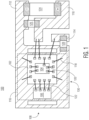
- FIG. 1 illustrates, in a simplified plan view, an example semiconductor device 100 having an embedded battery at a stage of manufacture in accordance with an embodiment.
- the semiconductor device 100 includes a sensor system 130, a battery 124, and components 126, 128 mounted on a package leadframe 108.
- the sensor system 130 is affixed to a die pad portion 116 of the leadframe 108 and the battery 124 is affixed to power legs 110, 112 of the leadframe 108.
- the term leg of the leadframe generally refers to a portion of the package leadframe suitable for connection of a bond wire and/or an internal component terminal (e.g., battery 124 and components 126, 128 terminals).
- Simplified side-on cross-sectional views of the example semiconductor device 100 taken are shown in stages of manufacture depicted in FIG. 2 and FIG. 3 .
- the sensor system 130 includes a controller subsystem 102, a wireless communication subsystem 106, and a sensor 104.
- the sensor system 130 is configured to sense environmental conditions, changes, and/or events and wirelessly communicate information based on the sensed conditions, changes, and/or events.
- the controller subsystem 102 includes circuitry configured to control functions of the sensor system 130 such as monitoring the sensor 104 and sending and/or receiving signals by way of the communication subsystem 106.
- the sensor system 130 may be implemented as a single system-on-chip (SoC) semiconductor die or may be implemented as a plurality of semiconductor die (e.g., one die per subsystem).
- SoC system-on-chip
- the controller subsystem 102 is formed as a semiconductor die 102 mounted on a die pad portion 116 of the leadframe 108.
- the sensor 104 is formed as a micro-electromechanical system (MEMS) semiconductor die 104 mounted on the first semiconductor die 102 and the communication subsystem 106 is formed as a semiconductor die 106 mounted on the die pad portion 116 of the leadframe.
- bond wires 118 interconnect the bond pads of the semiconductor die 102 with the leadframe 108
- bond wires 120 interconnect the bond pads of the semiconductor die 102 with the bond pads of the sensor 104
- bond wires 122 interconnect bond pads of the semiconductor die 102 with the bond pads of the communication semiconductor die 106.
- controller die 102 may be used interchangeably with the controller subsystem 102 and the semiconductor die 102.
- sensor die 104" may be used interchangeably with the sensor 104 and the MEMS semiconductor die 104, and the term “communication die 106” may be used interchangeably with the communication subsystem 106 and the semiconductor die 106.
- the controller subsystem 102 is coupled to the sensor 104 and the communication subsystem 106.
- the controller subsystem 102 may include circuitry configured to monitor one or more output signals from the sensor 104 and based on the one or more output signals, send communication signals (e.g., alerts, status indications, data) by way of the communication subsystem 106.
- the controller subsystem 102 may further include circuitry configured to receive communication signals (e.g., commands, information) by way of the communication subsystem 106.
- the controller die 102 has an active side (e.g., major side having circuitry, bond pads) and a backside (e.g., major side opposite of the active side).
- the controller die 102 includes bond pads located at the active side of the semiconductor die.
- the controller die 102 may be formed from any suitable semiconductor material, such as silicon, germanium, gallium arsenide, gallium nitride, and the like. In addition to the controller subsystem, the controller die 102 may further include any digital circuits, analog circuits, RF circuits, memory, processor, the like, and combinations thereof at the active side.
- the sensor 104 is coupled to the controller subsystem 102 and the communication subsystem 106.
- the sensor 104 may include any suitable sensor such as an accelerometer, pressure sensor, temperature sensor, etc.
- the sensor die 104 has an active side (e.g., major side having circuitry, bond pads) and a backside (e.g., major side opposite of the active side).
- the sensor die 104 includes bond pads located at the active side of the die.
- the sensor of the sensor die 104 may include one or more micromachined devices.
- the sensor die 104 may be formed from any suitable semiconductor material, such as silicon, germanium, gallium arsenide, gallium nitride, and the like.
- the sensor die 104 may further include any digital circuits, analog circuits, RF circuits, memory, processor, the like, and combinations thereof at the active side.
- the communication subsystem 106 is coupled to the controller subsystem 102 and the sensor 104.
- the communication subsystem 106 may include circuitry configured as a transmitter, receiver, or transceiver sufficient to communicate wirelessly with an external device separate from the semiconductor device 100.
- the communication subsystem 106 may communicate information based on an output signal of the sensor 104 of the sensor system 130.
- the communication subsystem 106 may further include an antenna.
- the communication subsystem 106 may be configured for one or more suitable wireless communication protocols (e.g., Bluetooth, Zigbee, Z-Wave, loT, Wi-Fi, cellular).
- the communication die 106 has an active side (e.g., major side having circuitry, bond pads) and a backside (e.g., major side opposite of the active side).
- the communication die 106 includes bond pads located at the active side of the die.
- the communication die 106 may be formed from any suitable semiconductor material, such as silicon, germanium, gallium arsenide, gallium nitride, and the like.
- the communication die 106 may further include any digital circuits, analog circuits, RF circuits, memory, processor, the like, and combinations thereof at the active side.
- the communication subsystem may be incorporated within the controller die 102 and the communication die 106 may serve as an antenna.
- the leadframe 108 includes power legs 110 and 112, signal leg 114, and die pad portion 116.
- the power legs 110 and 112 of the leadframe 108 are configured for connection of an internal power source (e.g., battery 124).
- the power leg 112 may be characterized as a ground power leg or ground leg 112 of the leadframe 108.
- the leadframe 108 may be formed from any suitable metal materials, such as copper, nickel, aluminum, iron, or alloys thereof, for example.
- the leadframe 108 may be bare, partially plated, or plated with another metal or alloy.
- the power legs 110 and 112, signal leg 114, and die pad portion 116 are all self-contained when encapsulated. Portions of the leadframe 108 such as tie bars and dam bars discarded during package singulation not shown for illustration purposes.
- the battery 124 may be characterized as a surface mount battery including terminals configured for attachment to the power legs 110 and 112 of the leadframe 108.
- the negative terminal (-) of the battery 124 is connected to the power (e.g., ground) leg 112 and die pad portion 116 and the positive terminal (+) of the battery 124 is connected to the power leg 110.
- the battery 124 may be formed as a single cell or plurality of cells configured to provide a predetermined nominal voltage and current capacity (e.g., 1.5 volts and 100 microampere-hours).
- the battery 124 is configured to supply an operating voltage and current to the sensor system 130 sufficient for the semiconductor device 100 to operate in a self-contained manner over a predetermined period of time.
- the battery 124 may be formed from any suitable materials and chemistries.
- the components 126 and 128 may be characterized as surface mount passive components (e.g., resistor, capacitor, inductor, diode) including terminals configured for attachment to the leadframe 108.
- the component 126 e.g., bypass capacitor
- the component 128 e.g., signal termination resistor
- the number, type, and location of surface mount passive components are examples chosen for illustrative purposes.
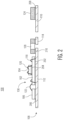
- FIG. 2 and FIG. 3 illustrate, in simplified side-on cross-sectional views, the example semiconductor device 100 at stages of manufacture in accordance with an embodiment.
- FIG. 2 illustrates, in a simplified side-on cross-sectional view, the example semiconductor device 100 at a stage of manufacture in accordance with an embodiment.
- the semiconductor device 100 includes the sensor system 130, battery 124, and components 126, 128 mounted on the package leadframe 108.
- the semiconductor die 102 of the sensor system 130 is mounted on the die pad portion of the leadframe 108 in an active-side-up orientation.
- the backside of the semiconductor die 102 is attached to top side of the die pad portion by way of a die attach material 202.
- the semiconductor die 106 of the sensor system 130 is mounted on the die pad portion of the leadframe 108 in an active-side-up orientation with the backside of the semiconductor die 106 attached to top side of the die pad portion by way of a die attach material 206.
- the sensor die 104 is mounted on the active side of the semiconductor die 102 in an active-side-up orientation with the backside of the sensor die 104 attached to active side of the semiconductor die 102 by way of a die attach material 204.
- the die attach materials 202 and 206 may be characterized as a conductive the die attach material and the die attach material 204 may be characterized as a non-conductive die attach material.
- die attach materials 202 and 206 may be formed as a silver-filled epoxy, solder paste, or conductive DAF and the die attach material 204 may be formed as a non-conductive epoxy or DAF. In other embodiments, other die attach materials and methods may be utilized.
- conductive as used herein, generally refers to the property of electrical conductivity.
- the positive terminal (+) of the battery 124 is conductively attached to the power leg 110 of the leadframe 108 by way of a conductive attachment material 208.
- a first terminal of the component 128 is conductively attached to the power leg 112 of the leadframe 108 and a second terminal of the component 128 is conductively attached to the signal leg 114 of the leadframe 108 by way of conductive attachment material 210.
- the die attach materials 208 and 210 may be characterized as conductive die attach materials such as silver-filled epoxy, solder paste, conductive DAF, or the like. It may be desirable to utilize a common attachment material for affixing the semiconductor die, battery terminals, and component terminals to the leadframe. In this manner, the assembly process can be streamlined and thus, reduce costs.
- the semiconductor die 102, sensor 104, and semiconductor die 106 of the sensor system 130 are interconnected with one another and the leadframe 108 by way of bond wires 118-122.
- a first set of bond pads (not shown) of the semiconductor die 102 are conductively connected to the leadframe 108 by way of bond wires 118.
- a second set of bond pads (not shown) of the semiconductor die 102 are conductively connected to the sensor 104 by way of bond wires 120
- a third set of bond pads (not shown) of the semiconductor die 102 are conductively connected to the semiconductor die 106 by way of bond wires 122.
- the bond wires 118-122 may be formed from a suitable metal material such as copper, silver, gold, or alloys thereof, for example.
- suitable metal material such as copper, silver, gold, or alloys thereof, for example.
- the number, location, and arrangement of bond wires 118-122 depicted in FIG. 2 are examples chosen for illustration purposes.
- bond wires 120 are configured to interconnect
- FIG. 3 illustrates, in a simplified side-on cross-sectional view, the example semiconductor device 100 at a subsequent stage of manufacture in accordance with an embodiment.
- the semiconductor device 100 is encapsulated and singulated.
- the semiconductor device 100 includes an encapsulant 302 encapsulating the sensor system 130, battery 124, components 126, 128, and package leadframe 108.
- the encapsulant 302 may be an epoxy molding compound dispensed during an injection molding encapsulation operation, for example.
- the semiconductor device 100 is singulated (e.g., trimmed) from remaining portions of a leadframe strip (e.g., tie bars) which may extend through and outside of the encapsulant.
- no portion of the leadframe 108 extends outside of the encapsulant for external connectivity.
- the semiconductor device 100 is configured to form a self-contained sensor system after encapsulation and singulation.
- the self-contained sensor system of the semiconductor device 100 includes an embedded battery power source configured to supply an operating voltage and current to the sensor system.
- the embedded battery power source is sufficient for the sensor system 130 of the semiconductor device 100 to operate (e.g., sense, monitor, communicate) in a self-contained manner over a predetermined period of time.
- an external antenna may be coupled to the sensor system 130 to augment wireless communication.
- an opening may be formed in the encapsulant 302 such that an external antenna may be affixed to the sensor system 130 in a manner sufficient to extend the range and/or enhance the quality of the wireless communication capabilities of the sensor system 130.
- a method of manufacturing a packaged semiconductor device including affixing a sensor system to a die pad portion of a leadframe; affixing a battery to the lead frame, a first terminal of the battery affixed to a first leg of the leadframe and a second terminal of the battery affixed to a second leg of the leadframe; and encapsulating with an encapsulant the sensor system, battery, and leadframe.
- the battery may be configured to supply an operating voltage and current to the sensor system.
- the sensor system may include a wireless communication subsystem configured for communication with an external device separate from the packaged semiconductor device, the communication including an output signal of the sensor system.
- the affixing the sensor system to the die pad portion may include affixing a semiconductor die to the die pad portion of the leadframe.
- the method may further include connecting a first bond pad of the semiconductor die to the first leg by way of a first bond wire and connecting a second bond pad of the semiconductor die to the second leg by way of a second bond wire.
- the sensor system may further include a MEMS sensor affixed to an active side of the semiconductor die.
- the method may further include, after encapsulating with the encapsulant, trimming to remove portions of the leadframe extending outside of the encapsulant.
- the second leg may be connected to the die pad portion of the leadframe.
- the method may further include, before encapsulating with the encapsulant, affixing a passive component to the lead frame, a first terminal of the passive component affixed to the first leg of the leadframe and a second terminal of the passive component affixed to the second leg of the leadframe, the passive component encapsulated by way of the encapsulating with the encapsulant.
- a semiconductor device including a sensor system affixed to a die pad portion of a leadframe; a battery affixed to the lead frame, a first terminal of the battery affixed to a first leg of the leadframe and a second terminal of the battery affixed to a second leg of the leadframe; and an encapsulant encapsulating the sensor system, battery, and leadframe.
- the battery may be configured to supply an operating voltage and current to the sensor system.
- the sensor system may include a wireless communication subsystem configured for communication with an external device separate from the packaged semiconductor device, the communication based on an output signal of the sensor system.
- the sensor system affixed to the die pad portion may include a semiconductor die affixed to the die pad portion of the leadframe.
- the semiconductor device may further include a first bond pad of the semiconductor die connected to the first leg by way of a first bond wire and a second bond pad of the semiconductor die connected to the second leg by way of a second bond wire.
- the encapsulated sensor system, battery, and leadframe may be configured to form a self-contained sensor system.
- a method of manufacturing a packaged semiconductor device including affixing a sensor system to a die pad portion of a leadframe; affixing a battery to the lead frame, a first terminal of the battery affixed to a first leg of the leadframe and a second terminal of the battery affixed to a second leg of the leadframe; and encapsulating with an encapsulant the sensor system, battery, and leadframe to form a self-contained sensor system.
- the battery may be configured to supply an operating voltage and current to the sensor system.
- the affixing the sensor system to the die pad portion may include affixing a semiconductor die to the die pad portion of the leadframe.
- the method may further include connecting a first bond pad of the semiconductor die to the first leg by way of a first bond wire and connecting a second bond pad of the semiconductor die to the second leg by way of a second bond wire.
- the sensor system may be configured to wirelessly transmit an output signal of the sensor system to an external device separate from the packaged semiconductor device.
- the semiconductor device includes one or more semiconductor die mounted on a package leadframe along with a battery mounted on the leadframe.
- the one or more semiconductor die, battery, and leadframe are encapsulated with an encapsulant.
- the semiconductor device is configured to operate using the battery as its power source.
- the semiconductor device is further configured to communicate wirelessly with an external device.
- the self-contained semiconductor device configured with wireless communication capability is especially useful for sensor systems, for example. In this manner, a self-contained, self-powered sensor system could be placed virtually anywhere.
Landscapes
- Engineering & Computer Science (AREA)
- Microelectronics & Electronic Packaging (AREA)
- Manufacturing & Machinery (AREA)
- Power Engineering (AREA)
- Die Bonding (AREA)
- Lead Frames For Integrated Circuits (AREA)
- Battery Mounting, Suspending (AREA)
Abstract
Description
- This disclosure relates generally to semiconductor devices, and more specifically, to semiconductor devices with an embedded battery and method of forming the same.
- Semiconductor devices are often found in a large spectrum of electronic products - from sewing machines to washing machines, from automobiles to cellular telephones, and so on. Many of these semiconductor devices may include sensitive systems and may be produced in high volumes to drive costs down. However, some factors such as manufacturing processes may be optimized for product costs but could adversely affect or constrain applications using these semiconductor devices. It is therefore desirable, as technology progresses, to accommodate flexible and less constrained applications of these semiconductor devices while keeping product costs in focus.
- The present invention is illustrated by way of example and is not limited by the accompanying figures, in which like references indicate similar elements. Elements in the figures are illustrated for simplicity and clarity and have not necessarily been drawn to scale.
-
FIG. 1 illustrates, in a simplified plan view, an example semiconductor device having an embedded battery at a stage of manufacture in accordance with an embodiment. -
FIG. 2 andFIG. 3 illustrate, in simplified side-on cross-sectional views, the example semiconductor device at stages of manufacture in accordance with an embodiment. - Generally, there is provided, a semiconductor device having an embedded battery. The semiconductor device includes one or more semiconductor die mounted on a package leadframe along with a battery mounted on the leadframe. The one or more semiconductor die, battery, and leadframe are encapsulated with an encapsulant. In a self-contained manner, the semiconductor device is configured to operate using the battery as its power source. The semiconductor device is further configured to communicate wirelessly with an external device. The self-contained semiconductor device configured with wireless communication capability is especially useful for sensor systems, for example. In this manner, a self-contained, self-powered sensor system could be placed virtually anywhere.
-
FIG. 1 illustrates, in a simplified plan view, anexample semiconductor device 100 having an embedded battery at a stage of manufacture in accordance with an embodiment. At this stage, thesemiconductor device 100 includes asensor system 130, abattery 124, andcomponents package leadframe 108. In this embodiment, thesensor system 130 is affixed to adie pad portion 116 of theleadframe 108 and thebattery 124 is affixed topower legs leadframe 108. The term leg of the leadframe, as used herein, generally refers to a portion of the package leadframe suitable for connection of a bond wire and/or an internal component terminal (e.g.,battery 124 andcomponents example semiconductor device 100 taken are shown in stages of manufacture depicted inFIG. 2 andFIG. 3 . - The
sensor system 130 includes acontroller subsystem 102, awireless communication subsystem 106, and asensor 104. Thesensor system 130 is configured to sense environmental conditions, changes, and/or events and wirelessly communicate information based on the sensed conditions, changes, and/or events. In this embodiment, thecontroller subsystem 102 includes circuitry configured to control functions of thesensor system 130 such as monitoring thesensor 104 and sending and/or receiving signals by way of thecommunication subsystem 106. Thesensor system 130 may be implemented as a single system-on-chip (SoC) semiconductor die or may be implemented as a plurality of semiconductor die (e.g., one die per subsystem). - In this embodiment, the
controller subsystem 102 is formed as asemiconductor die 102 mounted on adie pad portion 116 of theleadframe 108. Thesensor 104 is formed as a micro-electromechanical system (MEMS) semiconductor die 104 mounted on the first semiconductor die 102 and thecommunication subsystem 106 is formed as asemiconductor die 106 mounted on thedie pad portion 116 of the leadframe. In this embodiment,bond wires 118 interconnect the bond pads of the semiconductor die 102 with theleadframe 108,bond wires 120 interconnect the bond pads of thesemiconductor die 102 with the bond pads of thesensor 104, andbond wires 122 interconnect bond pads of the semiconductor die 102 with the bond pads of the communication semiconductor die 106. The number, location, and arrangement of bond pads and interconnectivity formed by bond wires 118-122 are examples chosen for illustration purposes. For discussion purposes herein, the term "controller die 102" may be used interchangeably with thecontroller subsystem 102 and the semiconductor die 102. Likewise, the term "sensor die 104" may be used interchangeably with thesensor 104 and the MEMS semiconductor die 104, and the term "communication die 106" may be used interchangeably with thecommunication subsystem 106 and thesemiconductor die 106. - The
controller subsystem 102 is coupled to thesensor 104 and thecommunication subsystem 106. Thecontroller subsystem 102 may include circuitry configured to monitor one or more output signals from thesensor 104 and based on the one or more output signals, send communication signals (e.g., alerts, status indications, data) by way of thecommunication subsystem 106. Thecontroller subsystem 102 may further include circuitry configured to receive communication signals (e.g., commands, information) by way of thecommunication subsystem 106. The controller die 102 has an active side (e.g., major side having circuitry, bond pads) and a backside (e.g., major side opposite of the active side). The controller die 102 includes bond pads located at the active side of the semiconductor die. The controller die 102 may be formed from any suitable semiconductor material, such as silicon, germanium, gallium arsenide, gallium nitride, and the like. In addition to the controller subsystem, the controller die 102 may further include any digital circuits, analog circuits, RF circuits, memory, processor, the like, and combinations thereof at the active side. - The
sensor 104 is coupled to thecontroller subsystem 102 and thecommunication subsystem 106. Thesensor 104 may include any suitable sensor such as an accelerometer, pressure sensor, temperature sensor, etc. The sensor die 104 has an active side (e.g., major side having circuitry, bond pads) and a backside (e.g., major side opposite of the active side). The sensor die 104 includes bond pads located at the active side of the die. The sensor of thesensor die 104 may include one or more micromachined devices. The sensor die 104 may be formed from any suitable semiconductor material, such as silicon, germanium, gallium arsenide, gallium nitride, and the like. In addition to the sensor, the sensor die 104 may further include any digital circuits, analog circuits, RF circuits, memory, processor, the like, and combinations thereof at the active side. - The
communication subsystem 106 is coupled to thecontroller subsystem 102 and thesensor 104. Thecommunication subsystem 106 may include circuitry configured as a transmitter, receiver, or transceiver sufficient to communicate wirelessly with an external device separate from thesemiconductor device 100. For example, thecommunication subsystem 106 may communicate information based on an output signal of thesensor 104 of thesensor system 130. Thecommunication subsystem 106 may further include an antenna. Thecommunication subsystem 106 may be configured for one or more suitable wireless communication protocols (e.g., Bluetooth, Zigbee, Z-Wave, loT, Wi-Fi, cellular). The communication die 106 has an active side (e.g., major side having circuitry, bond pads) and a backside (e.g., major side opposite of the active side). The communication die 106 includes bond pads located at the active side of the die. The communication die 106 may be formed from any suitable semiconductor material, such as silicon, germanium, gallium arsenide, gallium nitride, and the like. In addition to the communication subsystem, the communication die 106 may further include any digital circuits, analog circuits, RF circuits, memory, processor, the like, and combinations thereof at the active side. In some embodiments, the communication subsystem may be incorporated within the controller die 102 and the communication die 106 may serve as an antenna. - The
leadframe 108 includespower legs signal leg 114, anddie pad portion 116. Thepower legs leadframe 108 are configured for connection of an internal power source (e.g., battery 124). In this embodiment, thepower leg 112 may be characterized as a ground power leg orground leg 112 of theleadframe 108. Theleadframe 108 may be formed from any suitable metal materials, such as copper, nickel, aluminum, iron, or alloys thereof, for example. Theleadframe 108 may be bare, partially plated, or plated with another metal or alloy. In this embodiment, thepower legs signal leg 114, and diepad portion 116 are all self-contained when encapsulated. Portions of theleadframe 108 such as tie bars and dam bars discarded during package singulation not shown for illustration purposes. - The
battery 124 may be characterized as a surface mount battery including terminals configured for attachment to thepower legs leadframe 108. In this embodiment, the negative terminal (-) of thebattery 124 is connected to the power (e.g., ground)leg 112 and diepad portion 116 and the positive terminal (+) of thebattery 124 is connected to thepower leg 110. Thebattery 124 may be formed as a single cell or plurality of cells configured to provide a predetermined nominal voltage and current capacity (e.g., 1.5 volts and 100 microampere-hours). In this embodiment, thebattery 124 is configured to supply an operating voltage and current to thesensor system 130 sufficient for thesemiconductor device 100 to operate in a self-contained manner over a predetermined period of time. Thebattery 124 may be formed from any suitable materials and chemistries. - The
components leadframe 108. In this embodiment, the component 126 (e.g., bypass capacitor) is attached between thepower legs signal leg 114 and thepower leg 112. The number, type, and location of surface mount passive components are examples chosen for illustrative purposes. -
FIG. 2 andFIG. 3 illustrate, in simplified side-on cross-sectional views, theexample semiconductor device 100 at stages of manufacture in accordance with an embodiment. -
FIG. 2 illustrates, in a simplified side-on cross-sectional view, theexample semiconductor device 100 at a stage of manufacture in accordance with an embodiment. At this stage, thesemiconductor device 100 includes thesensor system 130,battery 124, andcomponents package leadframe 108. In this embodiment, the semiconductor die 102 of thesensor system 130 is mounted on the die pad portion of theleadframe 108 in an active-side-up orientation. For example, the backside of the semiconductor die 102 is attached to top side of the die pad portion by way of a die attachmaterial 202. Likewise, the semiconductor die 106 of thesensor system 130 is mounted on the die pad portion of theleadframe 108 in an active-side-up orientation with the backside of the semiconductor die 106 attached to top side of the die pad portion by way of a die attachmaterial 206. In this embodiment, the sensor die 104 is mounted on the active side of the semiconductor die 102 in an active-side-up orientation with the backside of the sensor die 104 attached to active side of the semiconductor die 102 by way of a die attachmaterial 204. In this embodiment, the die attachmaterials material 204 may be characterized as a non-conductive die attach material. For example, die attachmaterials material 204 may be formed as a non-conductive epoxy or DAF. In other embodiments, other die attach materials and methods may be utilized. The term conductive, as used herein, generally refers to the property of electrical conductivity. - In the embodiment of
FIG. 2 , the positive terminal (+) of thebattery 124 is conductively attached to thepower leg 110 of theleadframe 108 by way of aconductive attachment material 208. Similarly, a first terminal of thecomponent 128 is conductively attached to thepower leg 112 of theleadframe 108 and a second terminal of thecomponent 128 is conductively attached to thesignal leg 114 of theleadframe 108 by way ofconductive attachment material 210. In this embodiment, the die attachmaterials - After the
sensor system 130,battery 124, andcomponents package leadframe 108, the semiconductor die 102,sensor 104, and semiconductor die 106 of thesensor system 130 are interconnected with one another and theleadframe 108 by way of bond wires 118-122. For example, a first set of bond pads (not shown) of the semiconductor die 102 are conductively connected to theleadframe 108 by way ofbond wires 118. Likewise, a second set of bond pads (not shown) of the semiconductor die 102 are conductively connected to thesensor 104 by way ofbond wires 120, and a third set of bond pads (not shown) of the semiconductor die 102 are conductively connected to the semiconductor die 106 by way ofbond wires 122. The bond wires 118-122 may be formed from a suitable metal material such as copper, silver, gold, or alloys thereof, for example. The number, location, and arrangement of bond wires 118-122 depicted inFIG. 2 are examples chosen for illustration purposes.bond wires 120 are configured to interconnect -
FIG. 3 illustrates, in a simplified side-on cross-sectional view, theexample semiconductor device 100 at a subsequent stage of manufacture in accordance with an embodiment. At this stage, thesemiconductor device 100 is encapsulated and singulated. In this embodiment, thesemiconductor device 100 includes anencapsulant 302 encapsulating thesensor system 130,battery 124,components package leadframe 108. Theencapsulant 302 may be an epoxy molding compound dispensed during an injection molding encapsulation operation, for example. After the molding operation, thesemiconductor device 100 is singulated (e.g., trimmed) from remaining portions of a leadframe strip (e.g., tie bars) which may extend through and outside of the encapsulant. In this embodiment, no portion of theleadframe 108 extends outside of the encapsulant for external connectivity. - In this embodiment, the
semiconductor device 100 is configured to form a self-contained sensor system after encapsulation and singulation. For example, the self-contained sensor system of thesemiconductor device 100 includes an embedded battery power source configured to supply an operating voltage and current to the sensor system. The embedded battery power source is sufficient for thesensor system 130 of thesemiconductor device 100 to operate (e.g., sense, monitor, communicate) in a self-contained manner over a predetermined period of time. - In some embodiments, an external antenna may be coupled to the
sensor system 130 to augment wireless communication. For example, an opening may be formed in theencapsulant 302 such that an external antenna may be affixed to thesensor system 130 in a manner sufficient to extend the range and/or enhance the quality of the wireless communication capabilities of thesensor system 130. - Generally, there is provided, a method of manufacturing a packaged semiconductor device including affixing a sensor system to a die pad portion of a leadframe; affixing a battery to the lead frame, a first terminal of the battery affixed to a first leg of the leadframe and a second terminal of the battery affixed to a second leg of the leadframe; and encapsulating with an encapsulant the sensor system, battery, and leadframe. The battery may be configured to supply an operating voltage and current to the sensor system. The sensor system may include a wireless communication subsystem configured for communication with an external device separate from the packaged semiconductor device, the communication including an output signal of the sensor system. The affixing the sensor system to the die pad portion may include affixing a semiconductor die to the die pad portion of the leadframe. The method may further include connecting a first bond pad of the semiconductor die to the first leg by way of a first bond wire and connecting a second bond pad of the semiconductor die to the second leg by way of a second bond wire. The sensor system may further include a MEMS sensor affixed to an active side of the semiconductor die. The method may further include, after encapsulating with the encapsulant, trimming to remove portions of the leadframe extending outside of the encapsulant. The second leg may be connected to the die pad portion of the leadframe. The method may further include, before encapsulating with the encapsulant, affixing a passive component to the lead frame, a first terminal of the passive component affixed to the first leg of the leadframe and a second terminal of the passive component affixed to the second leg of the leadframe, the passive component encapsulated by way of the encapsulating with the encapsulant.
- In another embodiment, there is provided, a semiconductor device including a sensor system affixed to a die pad portion of a leadframe; a battery affixed to the lead frame, a first terminal of the battery affixed to a first leg of the leadframe and a second terminal of the battery affixed to a second leg of the leadframe; and an encapsulant encapsulating the sensor system, battery, and leadframe. The battery may be configured to supply an operating voltage and current to the sensor system. The sensor system may include a wireless communication subsystem configured for communication with an external device separate from the packaged semiconductor device, the communication based on an output signal of the sensor system. The sensor system affixed to the die pad portion may include a semiconductor die affixed to the die pad portion of the leadframe. The semiconductor device may further include a first bond pad of the semiconductor die connected to the first leg by way of a first bond wire and a second bond pad of the semiconductor die connected to the second leg by way of a second bond wire. The encapsulated sensor system, battery, and leadframe may be configured to form a self-contained sensor system.
- In yet another embodiment, there is provided, a method of manufacturing a packaged semiconductor device including affixing a sensor system to a die pad portion of a leadframe; affixing a battery to the lead frame, a first terminal of the battery affixed to a first leg of the leadframe and a second terminal of the battery affixed to a second leg of the leadframe; and encapsulating with an encapsulant the sensor system, battery, and leadframe to form a self-contained sensor system. The battery may be configured to supply an operating voltage and current to the sensor system. The affixing the sensor system to the die pad portion may include affixing a semiconductor die to the die pad portion of the leadframe. The method may further include connecting a first bond pad of the semiconductor die to the first leg by way of a first bond wire and connecting a second bond pad of the semiconductor die to the second leg by way of a second bond wire. The sensor system may be configured to wirelessly transmit an output signal of the sensor system to an external device separate from the packaged semiconductor device.
- By now it should be appreciated that there has been provided, a semiconductor device having an embedded battery. The semiconductor device includes one or more semiconductor die mounted on a package leadframe along with a battery mounted on the leadframe. The one or more semiconductor die, battery, and leadframe are encapsulated with an encapsulant. In a self-contained manner, the semiconductor device is configured to operate using the battery as its power source. The semiconductor device is further configured to communicate wirelessly with an external device. The self-contained semiconductor device configured with wireless communication capability is especially useful for sensor systems, for example. In this manner, a self-contained, self-powered sensor system could be placed virtually anywhere.
- Although the invention is described herein with reference to specific embodiments, various modifications and changes can be made without departing from the scope of the present invention as set forth in the claims below. Accordingly, the specification and figures are to be regarded in an illustrative rather than a restrictive sense, and all such modifications are intended to be included within the scope of the present invention. Any benefits, advantages, or solutions to problems that are described herein with regard to specific embodiments are not intended to be construed as a critical, required, or essential feature or element of any or all the claims.
- Furthermore, the terms "a" or "an," as used herein, are defined as one or more than one. Also, the use of introductory phrases such as "at least one" and "one or more" in the claims should not be construed to imply that the introduction of another claim element by the indefinite articles "a" or "an" limits any particular claim containing such introduced claim element to inventions containing only one such element, even when the same claim includes the introductory phrases "one or more" or "at least one" and indefinite articles such as "a" or "an." The same holds true for the use of definite articles.
- Unless stated otherwise, terms such as "first" and "second" are used to arbitrarily distinguish between the elements such terms describe. Thus, these terms are not necessarily intended to indicate temporal or other prioritization of such elements.
Claims (15)
- A method of manufacturing a packaged semiconductor device, the method comprising:affixing a sensor system to a die pad portion of a leadframe;affixing a battery to the lead frame, a first terminal of the battery affixed to a first leg of the leadframe and a second terminal of the battery affixed to a second leg of the leadframe; andencapsulating with an encapsulant the sensor system, battery, and leadframe.
- The method of claim 1, wherein the battery is configured to supply an operating voltage and current to the sensor system.
- The method of any of claims 1 to 2, wherein the sensor system includes a wireless communication subsystem configured for communication with an external device separate from the packaged semiconductor device, the communication including an output signal of the sensor system.
- The method of any of claims 1 to 3, wherein affixing the sensor system to the die pad portion includes affixing a semiconductor die to the die pad portion of the leadframe.
- The method of claim 4, further comprising connecting a first bond pad of the semiconductor die to the first leg by way of a first bond wire and connecting a second bond pad of the semiconductor die to the second leg by way of a second bond wire.
- The method of claim 4 or 5, wherein the sensor system further includes a MEMS sensor affixed to an active side of the semiconductor die.
- The method of any of claims 1 to 6, further comprising, after encapsulating with the encapsulant, trimming to remove portions of the leadframe extending outside of the encapsulant.
- The method of any of claims 1 to 7, wherein the second leg is connected to the die pad portion of the leadframe.
- The method of any of claims 1 to 8, further comprising, before encapsulating with the encapsulant, affixing a passive component to the lead frame, a first terminal of the passive component affixed to the first leg of the leadframe and a second terminal of the passive component affixed to the second leg of the leadframe, the passive component encapsulated by way of the encapsulating with the encapsulant.
- A semiconductor device comprising:a sensor system affixed to a die pad portion of a leadframe;a battery affixed to the lead frame, a first terminal of the battery affixed to a first leg of the leadframe and a second terminal of the battery affixed to a second leg of the leadframe; andan encapsulant encapsulating the sensor system, battery, and leadframe.
- The semiconductor device of claim 10, wherein the battery is configured to supply an operating voltage and current to the sensor system.
- The semiconductor device of claim 10 or 11, wherein the sensor system includes a wireless communication subsystem configured for communication with an external device separate from the packaged semiconductor device, the communication based on an output signal of the sensor system.
- The semiconductor device of any of claims 10 to 12, wherein the sensor system affixed to the die pad portion includes a semiconductor die affixed to the die pad portion of the leadframe.
- The semiconductor device of any of claims 10 to 13, further comprising a first bond pad of the semiconductor die connected to the first leg by way of a first bond wire and a second bond pad of the semiconductor die connected to the second leg by way of a second bond wire.
- The semiconductor device of any of claims 10 to 14, wherein the encapsulated sensor system, battery, and leadframe are configured to form a self-contained sensor system.
Applications Claiming Priority (1)
| Application Number | Priority Date | Filing Date | Title |
|---|---|---|---|
| US17/660,650 US12406911B2 (en) | 2022-04-26 | 2022-04-26 | Semiconductor device with embedded battery and method therefor |
Publications (1)
| Publication Number | Publication Date |
|---|---|
| EP4269330A1 true EP4269330A1 (en) | 2023-11-01 |
Family
ID=85985251
Family Applications (1)
| Application Number | Title | Priority Date | Filing Date |
|---|---|---|---|
| EP23167092.8A Pending EP4269330A1 (en) | 2022-04-26 | 2023-04-06 | Semiconductor device with embedded battery and method therefor |
Country Status (3)
| Country | Link |
|---|---|
| US (2) | US12406911B2 (en) |
| EP (1) | EP4269330A1 (en) |
| CN (1) | CN116959998A (en) |
Families Citing this family (2)
| Publication number | Priority date | Publication date | Assignee | Title |
|---|---|---|---|---|
| US20240201778A1 (en) * | 2020-07-07 | 2024-06-20 | Micron Electronics LLC | Methdo and system of wireless device power management |
| US20240258212A1 (en) * | 2023-01-30 | 2024-08-01 | Texas Instruments Incorporated | Substrate-on-die package architecture |
Citations (3)
| Publication number | Priority date | Publication date | Assignee | Title |
|---|---|---|---|---|
| US20190109072A1 (en) * | 2017-10-06 | 2019-04-11 | Allegro Microsystems, Llc | Integrated Circuit Package Having A Raised Lead Edge |
| US10340211B1 (en) * | 2018-03-15 | 2019-07-02 | Nxp B.V. | Sensor module with blade insert |
| US20200321286A1 (en) * | 2019-04-05 | 2020-10-08 | Nxp Usa, Inc. | Media shield with emi capability for pressure sensor |
Family Cites Families (16)
| Publication number | Priority date | Publication date | Assignee | Title |
|---|---|---|---|---|
| US4998888A (en) | 1984-07-23 | 1991-03-12 | Sgs-Thomson Microelectronics, Inc. | Integrated circuit package with battery housing |
| US5180645A (en) | 1991-03-01 | 1993-01-19 | Motorola, Inc. | Integral solid state embedded power supply |
| US6045652A (en) * | 1992-06-17 | 2000-04-04 | Micron Communications, Inc. | Method of manufacturing an enclosed transceiver |
| US5403782A (en) | 1992-12-21 | 1995-04-04 | Sgs-Thomson Microelectronics, Inc. | Surface mountable integrated circuit package with integrated battery mount |
| US6109530A (en) | 1998-07-08 | 2000-08-29 | Motorola, Inc. | Integrated circuit carrier package with battery coin cell |
| US6284406B1 (en) * | 2000-06-09 | 2001-09-04 | Ntk Powerdex, Inc. | IC card with thin battery |
| US6809646B1 (en) * | 2001-12-06 | 2004-10-26 | Applied Wireless Identifications Group, Inc. | Thin implantable RFID transponder suitable for use in an identification badge |
| US7088074B2 (en) | 2002-01-02 | 2006-08-08 | International Business Machines Corporation | System level device for battery and integrated circuit integration |
| US6998692B2 (en) | 2003-10-14 | 2006-02-14 | Qynergy Corporation | IC package with an integrated power source |
| US9710126B2 (en) * | 2013-10-17 | 2017-07-18 | Blackberry Limited | Method and apparatus for displaying a preview of an application to a user |
| US9871273B2 (en) | 2014-12-18 | 2018-01-16 | Intel Corporation | Surface mount battery and portable electronic device with integrated battery cell |
| US9688530B2 (en) * | 2015-05-27 | 2017-06-27 | Texas Instruments Incorporated | Integrated circuit package with sensor and method of making |
| DE102016101433A1 (en) * | 2016-01-27 | 2017-07-27 | Infineon Technologies Ag | Multi-chip semiconductor power housing |
| CN106920786B (en) * | 2016-03-16 | 2018-11-06 | 三星半导体(中国)研究开发有限公司 | The packaging part of integrated power supply module |
| DE102020203235A1 (en) * | 2020-03-13 | 2021-09-16 | Hyundai Motor Company | SYSTEM AND PROCEDURE FOR SELLING CONSUMER GOODS IN A VEHICLE |
| US12469773B2 (en) * | 2022-11-29 | 2025-11-11 | Nxp Usa, Inc. | Semiconductor device with attached battery and method therefor |
-
2022
- 2022-04-26 US US17/660,650 patent/US12406911B2/en active Active
-
2023
- 2023-03-27 CN CN202310308484.5A patent/CN116959998A/en active Pending
- 2023-04-06 EP EP23167092.8A patent/EP4269330A1/en active Pending
-
2025
- 2025-05-08 US US19/202,438 patent/US20250266335A1/en active Pending
Patent Citations (3)
| Publication number | Priority date | Publication date | Assignee | Title |
|---|---|---|---|---|
| US20190109072A1 (en) * | 2017-10-06 | 2019-04-11 | Allegro Microsystems, Llc | Integrated Circuit Package Having A Raised Lead Edge |
| US10340211B1 (en) * | 2018-03-15 | 2019-07-02 | Nxp B.V. | Sensor module with blade insert |
| US20200321286A1 (en) * | 2019-04-05 | 2020-10-08 | Nxp Usa, Inc. | Media shield with emi capability for pressure sensor |
Also Published As
| Publication number | Publication date |
|---|---|
| US20250266335A1 (en) | 2025-08-21 |
| US12406911B2 (en) | 2025-09-02 |
| CN116959998A (en) | 2023-10-27 |
| US20230343683A1 (en) | 2023-10-26 |
Similar Documents
| Publication | Publication Date | Title |
|---|---|---|
| US20250266335A1 (en) | Semiconductor device with embedded battery and method therefor | |
| US8802474B1 (en) | Pressure sensor and method of packaging same | |
| US6201186B1 (en) | Electronic component assembly and method of making the same | |
| US8018036B2 (en) | Ultra-thin quad flat no-lead (QFN) package | |
| US20140374848A1 (en) | Semiconductor sensor device with metal lid | |
| US20260053012A1 (en) | Semiconductor device with attached battery and method therefor | |
| US20170047271A1 (en) | Method for making a semiconductor device having an interposer | |
| US20050263861A1 (en) | Integrated circuit leadframe and fabrication method therefor | |
| US6798046B1 (en) | Semiconductor package including ring structure connected to leads with vertically downset inner ends | |
| US6696749B1 (en) | Package structure having tapering support bars and leads | |
| CN104016296B (en) | The method for packing of a kind of encapsulating structure and this encapsulating structure | |
| US11222790B2 (en) | Tie bar removal for semiconductor device packaging | |
| EP4086952A1 (en) | Semiconductor device packaging leadframe assembly and method therefor | |
| EP3647755A1 (en) | Sensor device with flip-chip die and interposer | |
| EP4593080A1 (en) | Semiconductor device with dual downset leadframe and method therefor | |
| EP3761360B1 (en) | Power die package | |
| US8987881B2 (en) | Hybrid lead frame and ball grid array package | |
| US12125780B2 (en) | Extendable inner lead for leaded package | |
| US20170081178A1 (en) | Semiconductor device package with seal structure | |
| US20210013137A1 (en) | Semiconductor device with lead frame that accommodates various die sizes | |
| EP4704543A1 (en) | Semiconductor device with hybrid multi-die package and method therefor | |
| EP4525027A1 (en) | Semiconductor device with enhanced solderability and method therefor | |
| EP4485529A1 (en) | Semiconductor device with leadframe spacer and method therefor | |
| CN221008933U (en) | Short message communication chip module and communication terminal | |
| EP4481808A1 (en) | Dual leadframe semiconductor device and method therefor |
Legal Events
| Date | Code | Title | Description |
|---|---|---|---|
| PUAI | Public reference made under article 153(3) epc to a published international application that has entered the european phase |
Free format text: ORIGINAL CODE: 0009012 |
|
| STAA | Information on the status of an ep patent application or granted ep patent |
Free format text: STATUS: THE APPLICATION HAS BEEN PUBLISHED |
|
| AK | Designated contracting states |
Kind code of ref document: A1 Designated state(s): AL AT BE BG CH CY CZ DE DK EE ES FI FR GB GR HR HU IE IS IT LI LT LU LV MC ME MK MT NL NO PL PT RO RS SE SI SK SM TR |
|
| STAA | Information on the status of an ep patent application or granted ep patent |
Free format text: STATUS: REQUEST FOR EXAMINATION WAS MADE |
|
| 17P | Request for examination filed |
Effective date: 20240502 |
|
| RBV | Designated contracting states (corrected) |
Designated state(s): AL AT BE BG CH CY CZ DE DK EE ES FI FR GB GR HR HU IE IS IT LI LT LU LV MC ME MK MT NL NO PL PT RO RS SE SI SK SM TR |
|
| STAA | Information on the status of an ep patent application or granted ep patent |
Free format text: STATUS: EXAMINATION IS IN PROGRESS |
|
| 17Q | First examination report despatched |
Effective date: 20250926 |
|
| RAP1 | Party data changed (applicant data changed or rights of an application transferred) |
Owner name: STMICROELECTRONICS INTERNATIONAL N.V. |