EP4266381A2 - Solder strip and solar cell module - Google Patents
Solder strip and solar cell module Download PDFInfo
- Publication number
- EP4266381A2 EP4266381A2 EP23196698.7A EP23196698A EP4266381A2 EP 4266381 A2 EP4266381 A2 EP 4266381A2 EP 23196698 A EP23196698 A EP 23196698A EP 4266381 A2 EP4266381 A2 EP 4266381A2
- Authority
- EP
- European Patent Office
- Prior art keywords
- side edge
- angle
- solder strip
- edge
- base portion
- Prior art date
- Legal status (The legal status is an assumption and is not a legal conclusion. Google has not performed a legal analysis and makes no representation as to the accuracy of the status listed.)
- Pending
Links
Images




Classifications
-
- H—ELECTRICITY
- H10—SEMICONDUCTOR DEVICES; ELECTRIC SOLID-STATE DEVICES NOT OTHERWISE PROVIDED FOR
- H10F—INORGANIC SEMICONDUCTOR DEVICES SENSITIVE TO INFRARED RADIATION, LIGHT, ELECTROMAGNETIC RADIATION OF SHORTER WAVELENGTH OR CORPUSCULAR RADIATION
- H10F77/00—Constructional details of devices covered by this subclass
- H10F77/20—Electrodes
- H10F77/206—Electrodes for devices having potential barriers
- H10F77/211—Electrodes for devices having potential barriers for photovoltaic cells
- H10F77/215—Geometries of grid contacts
-
- H—ELECTRICITY
- H10—SEMICONDUCTOR DEVICES; ELECTRIC SOLID-STATE DEVICES NOT OTHERWISE PROVIDED FOR
- H10F—INORGANIC SEMICONDUCTOR DEVICES SENSITIVE TO INFRARED RADIATION, LIGHT, ELECTROMAGNETIC RADIATION OF SHORTER WAVELENGTH OR CORPUSCULAR RADIATION
- H10F19/00—Integrated devices, or assemblies of multiple devices, comprising at least one photovoltaic cell covered by group H10F10/00, e.g. photovoltaic modules
- H10F19/90—Structures for connecting between photovoltaic cells, e.g. interconnections or insulating spacers
- H10F19/902—Structures for connecting between photovoltaic cells, e.g. interconnections or insulating spacers for series or parallel connection of photovoltaic cells
- H10F19/906—Structures for connecting between photovoltaic cells, e.g. interconnections or insulating spacers for series or parallel connection of photovoltaic cells characterised by the materials of the structures
-
- H—ELECTRICITY
- H10—SEMICONDUCTOR DEVICES; ELECTRIC SOLID-STATE DEVICES NOT OTHERWISE PROVIDED FOR
- H10F—INORGANIC SEMICONDUCTOR DEVICES SENSITIVE TO INFRARED RADIATION, LIGHT, ELECTROMAGNETIC RADIATION OF SHORTER WAVELENGTH OR CORPUSCULAR RADIATION
- H10F19/00—Integrated devices, or assemblies of multiple devices, comprising at least one photovoltaic cell covered by group H10F10/00, e.g. photovoltaic modules
- H10F19/80—Encapsulations or containers for integrated devices, or assemblies of multiple devices, having photovoltaic cells
-
- H—ELECTRICITY
- H10—SEMICONDUCTOR DEVICES; ELECTRIC SOLID-STATE DEVICES NOT OTHERWISE PROVIDED FOR
- H10F—INORGANIC SEMICONDUCTOR DEVICES SENSITIVE TO INFRARED RADIATION, LIGHT, ELECTROMAGNETIC RADIATION OF SHORTER WAVELENGTH OR CORPUSCULAR RADIATION
- H10F19/00—Integrated devices, or assemblies of multiple devices, comprising at least one photovoltaic cell covered by group H10F10/00, e.g. photovoltaic modules
- H10F19/80—Encapsulations or containers for integrated devices, or assemblies of multiple devices, having photovoltaic cells
- H10F19/807—Double-glass encapsulation, e.g. photovoltaic cells arranged between front and rear glass sheets
-
- H—ELECTRICITY
- H10—SEMICONDUCTOR DEVICES; ELECTRIC SOLID-STATE DEVICES NOT OTHERWISE PROVIDED FOR
- H10F—INORGANIC SEMICONDUCTOR DEVICES SENSITIVE TO INFRARED RADIATION, LIGHT, ELECTROMAGNETIC RADIATION OF SHORTER WAVELENGTH OR CORPUSCULAR RADIATION
- H10F19/00—Integrated devices, or assemblies of multiple devices, comprising at least one photovoltaic cell covered by group H10F10/00, e.g. photovoltaic modules
- H10F19/80—Encapsulations or containers for integrated devices, or assemblies of multiple devices, having photovoltaic cells
- H10F19/85—Protective back sheets
-
- H—ELECTRICITY
- H10—SEMICONDUCTOR DEVICES; ELECTRIC SOLID-STATE DEVICES NOT OTHERWISE PROVIDED FOR
- H10F—INORGANIC SEMICONDUCTOR DEVICES SENSITIVE TO INFRARED RADIATION, LIGHT, ELECTROMAGNETIC RADIATION OF SHORTER WAVELENGTH OR CORPUSCULAR RADIATION
- H10F19/00—Integrated devices, or assemblies of multiple devices, comprising at least one photovoltaic cell covered by group H10F10/00, e.g. photovoltaic modules
- H10F19/90—Structures for connecting between photovoltaic cells, e.g. interconnections or insulating spacers
- H10F19/902—Structures for connecting between photovoltaic cells, e.g. interconnections or insulating spacers for series or parallel connection of photovoltaic cells
- H10F19/904—Structures for connecting between photovoltaic cells, e.g. interconnections or insulating spacers for series or parallel connection of photovoltaic cells characterised by the shapes of the structures
-
- H—ELECTRICITY
- H10—SEMICONDUCTOR DEVICES; ELECTRIC SOLID-STATE DEVICES NOT OTHERWISE PROVIDED FOR
- H10F—INORGANIC SEMICONDUCTOR DEVICES SENSITIVE TO INFRARED RADIATION, LIGHT, ELECTROMAGNETIC RADIATION OF SHORTER WAVELENGTH OR CORPUSCULAR RADIATION
- H10F77/00—Constructional details of devices covered by this subclass
- H10F77/40—Optical elements or arrangements
- H10F77/42—Optical elements or arrangements directly associated or integrated with photovoltaic cells, e.g. light-reflecting means or light-concentrating means
- H10F77/488—Reflecting light-concentrating means, e.g. parabolic mirrors or concentrators using total internal reflection
-
- H—ELECTRICITY
- H10—SEMICONDUCTOR DEVICES; ELECTRIC SOLID-STATE DEVICES NOT OTHERWISE PROVIDED FOR
- H10F—INORGANIC SEMICONDUCTOR DEVICES SENSITIVE TO INFRARED RADIATION, LIGHT, ELECTROMAGNETIC RADIATION OF SHORTER WAVELENGTH OR CORPUSCULAR RADIATION
- H10F77/00—Constructional details of devices covered by this subclass
- H10F77/93—Interconnections
- H10F77/933—Interconnections for devices having potential barriers
- H10F77/935—Interconnections for devices having potential barriers for photovoltaic devices or modules
- H10F77/937—Busbar structures for modules
-
- Y—GENERAL TAGGING OF NEW TECHNOLOGICAL DEVELOPMENTS; GENERAL TAGGING OF CROSS-SECTIONAL TECHNOLOGIES SPANNING OVER SEVERAL SECTIONS OF THE IPC; TECHNICAL SUBJECTS COVERED BY FORMER USPC CROSS-REFERENCE ART COLLECTIONS [XRACs] AND DIGESTS
- Y02—TECHNOLOGIES OR APPLICATIONS FOR MITIGATION OR ADAPTATION AGAINST CLIMATE CHANGE
- Y02E—REDUCTION OF GREENHOUSE GAS [GHG] EMISSIONS, RELATED TO ENERGY GENERATION, TRANSMISSION OR DISTRIBUTION
- Y02E10/00—Energy generation through renewable energy sources
- Y02E10/50—Photovoltaic [PV] energy
-
- Y—GENERAL TAGGING OF NEW TECHNOLOGICAL DEVELOPMENTS; GENERAL TAGGING OF CROSS-SECTIONAL TECHNOLOGIES SPANNING OVER SEVERAL SECTIONS OF THE IPC; TECHNICAL SUBJECTS COVERED BY FORMER USPC CROSS-REFERENCE ART COLLECTIONS [XRACs] AND DIGESTS
- Y02—TECHNOLOGIES OR APPLICATIONS FOR MITIGATION OR ADAPTATION AGAINST CLIMATE CHANGE
- Y02E—REDUCTION OF GREENHOUSE GAS [GHG] EMISSIONS, RELATED TO ENERGY GENERATION, TRANSMISSION OR DISTRIBUTION
- Y02E10/00—Energy generation through renewable energy sources
- Y02E10/50—Photovoltaic [PV] energy
- Y02E10/52—PV systems with concentrators
Definitions
- the present disclosure relates to the field of photovoltaic solder strip technologies, and in particular, to a solder strip and a solar cell module.
- a solder strip is also referred to as an interconnection strip or a bus bar, and is an important raw material during soldering of a photovoltaic module.
- the solder strip generally connects solar cells to each other and converges currents by soldering or conductive adhesive bonding. Quality of the solder strip may directly affect efficiency of current collection of the photovoltaic module and may have a considerable influence on power of the photovoltaic module. Cross sections of solder strips are mostly rectangular.
- An objective of the present disclosure is to provide a solder strip and a solar cell module, so as to solve the technical problems in the related art.
- a cross section of the solder strip includes a base portion and a reflective portion arranged above the base portion.
- the reflective portion includes a top edge, a first side edge and a second side edge. One end of the first side edge and one end of the second side edge continue from the top edge, and the other end of the first side edge and the other end of the second side edge continue from the base portion.
- a first angle is formed between the first side edge and an extension line of the top edge, and a second angle is formed between the second side edge and the extension line of the top edge. The first angle and the second angle are both acute angles formed in a range greater than 42.5°.
- the first angle and the second angle are formed in a range between 60° and 70°.
- the first side edge and/or the second side edge includes a plurality of continuous folded sections, and an angle between each of the plurality of continuous folded sections and the extension line of the bottom edge of the base portion is an acute angles formed in a range greater than 42.5°.
- a height of the cross-section of the solder strip is within a range of 60% to 80% of a width of the cross-section.
- the height of the cross-section of the solder strip is less than or equal to 0.3 mm.
- the base portion has a width of 0.4 ⁇ 0.1 mm and a height of 0.18 ⁇ 0.02 mm, and the reflective portion has a height of 0.09 ⁇ 0.01 mm.
- the base portion has a width of 0.41 mm and a height of 0.2 mm or a width of 0.4 mm and a height of 0.17 mm, and the reflective portion has a height of 0.1 mm.
- the base portion further includes a third side edge and a fourth side edge, and the third side edge and the fourth side edge are arranged opposite to each other. Two opposite ends of the third side edge are connected to the bottom edge and the first side edge, respectively, and a third angle is formed between the third side edge and the bottom edge. Two opposite ends of the fourth side edge are connected to the bottom edge and the second side edge, respectively, and a fourth angle is formed between the fourth side edge and the bottom edge.
- the third angle and the fourth angle are formed in a range between 90° and 120°.
- the third angle and/or the fourth angle is an acute angle.
- the solder strip includes a copper substrate and a solder layer coated on a surface of the copper substrate.
- the copper substrate is made of pure copper, oxygen-free copper or red copper
- the solder layer is made of pure tin, a tin-lead mixture or a tin-lead-silver mixture.
- the solder layer has a thickness in a range of 10 ⁇ m to 15 ⁇ m.
- the present disclosure further provides a solar cell module.
- the solar cell module includes a back plate, packaging glass and a plurality of solar cells. Adjacent solar cells of the plurality of solar cells are electrically connected through a solder strip.
- the back plate is arranged below the plurality of solar cells
- the packaging glass is located above the plurality of solar cells, and a space between the back plate and the plurality of solar cells and a space between the packaging glass and the plurality of solar cells are filled with a packaging adhesive film.
- the solder strip includes a main body section. A cross section of the main body section includes a base portion and a reflective portion arranged above the base portion.
- the reflective portion includes a top edge, a fifth side edge and a sixth side edge, and the fifth side edge and the sixth side edge are each of a convex arc-surface structure.
- One end of the fifth side edge and one end of the sixth side edge continue from the top edge, and the other end of the fifth side edge and the other end of the sixth side edge continue from the base portion.
- a fifth angle is formed between a tangent line of a midpoint of the fifth side edge and an extension line of a bottom edge of the base portion
- a sixth angle is formed between a tangent line of a midpoint of the sixth side edge and the extension line of the bottom edge of the base portion.
- the fifth angle and the sixth angle are both acute angles formed in a range greater than 42.5°.
- the solder strip further includes a flat section connected to the main body section.
- the main body section is welded to a busbar of the plurality of solar cells, and the flat section is located between two of the plurality of solar cells.
- the flat section is of a flat elongated strip structure, and a bottom edge of the flat section is parallel to a bottom edge of the base portion.
- the fifth angle and the sixth angle are formed in a range between 60° and 70°.
- a height of the cross-section of the solder strip is within a range of 60% to 80% of a width of the cross-section.
- the height of the cross-section of the solder strip is less than or equal to 0.3 mm.
- the base portion has a width of 0.4 ⁇ 0.1 mm and a height of 0.18 ⁇ 0.02 mm, and the reflective portion has a height of 0.09 ⁇ 0.01 mm.
- the base portion has a width of 0.41 mm and a height of 0.2 mm or a width of 0.4 mm and a height of 0.17 mm, and the reflective portion has a height of 0.1 mm.
- the base portion further includes a seventh side edge and an eighth side edge, the seventh side edge and the eighth side edge being arranged opposite to each other. Two opposite ends of the seventh side edge are connected to the bottom edge and the fifth side edge, respectively. Two opposite ends of the eighth side edge are connected to the bottom edge and the sixth side edge respectively. An arc-surface transition is formed between the seventh side edge and the bottom edge and between the eighth side edge and the bottom edge.
- an agglomeration layer is formed between the base portion and the plurality of solar cells, and the agglomeration layer is formed by molten accumulation of the solder layer.
- an embodiment of the present disclosure provides a solder strip 16.
- the solder strip 16 is of an elongated strip structure. Across section of the solder strip 16 includes a base portion 1 and a reflective portion 2 arranged above the base portion 1.
- the reflective portion 2 and the base portion 1 may have an integrated structure, and the division into two parts is only for functional description.
- the reflective portion 2 includes a top edge 3, a first side edge 4 and a second side edge 5. One end of the first side edge 4 and one end of the second side edge 5 continue from the top edge 3. The other end of the first side edge 4 and the other end of the second side edge 5 continue from the base portion 1.
- a first angle 6 is formed between the first side edge 4 and an extension line of a bottom edge 8 of the base portion 1
- a second angle 7 is formed between the second side edge 5 and the extension line of the bottom edge 8 of the base portion 1
- the first angle 6 and the second angle 7 are both greater than 42.5° and less than 90° (excluding 90°).
- the first angle 6 and/or the second angle 7 are/is greater than 42.5° and less than 90°, referring to FIG. 5 , after reflected light incident on the solder strip 16 in a direction perpendicular to the second side edge 5 strikes packaging glass 13, an incident angle (an angle between the reflected light and a normal line of the packaging glass 13) is equal to the second angle 7.
- the reflected light incident on the solder strip 16 may be totally reflected at a glass and air interface layer of the solar cell module, so that the sunlight totally reflected re-participates in photoelectric conversion and thus improves the utilization of the reflected light.
- the reflected light on the solder strip 16 may be totally reflected to a solar cell 14 to participate in photoelectric conversion after the first angle 6 and the second angle 7 are equal to or greater than the critical angle. If the first angle 6 and the second angle 7 are less than the angle, the reflected light on the solder strip 16 cannot meet requirements on total reflection and may pass through the packaging glass 13 of the solar cell module, and thus cannot be utilized.
- the first angle 6 is equal to the second angle 7, that is, the first side edge 4 and the second side edge 5 are arranged symmetrically with respect to a perpendicular bisector of the bottom edge 8 of the base portion 1, which has a symmetrically distributed structure, facilitates processing and forming, and can evenly reflect the sunlight to the solar cells 14 on two sides, so as to improve reflection efficiency.
- first angle 6 and the second angle 7 are between 60° and 70°, on the one hand, a purpose that the first angle 6 and the second angle 7 are greater than the critical angle at which the sunlight is totally reflected at the glass and air interface layer of the photovoltaic cell module can be achieved.
- accumulation caused by melting of a solder layer 18 during the soldering of the solder strip 16 is also prevented, so that thicknesses of the first side edge 4 and the second side edge 5 are increased, thereby reducing the first angle 6 and the second angle 7.
- the first angle 6 and the second angle 7 are both set to 60° to 70° so that a margin can be remained. In a case where the solder layer 18 is accumulated, the first angle 6 and the second angle 7 are still greater than the critical angle at which the sunlight is totally reflected at the glass and air interface layer of the solar cell module.
- the height of the cross-section of the solder strip 16 is designed to be less than 0.3 mm, in a case where the solder strip 16 has a same copper substrate 17 as a round-wire solder strip 16 (i.e., a same power is maintained), a weight of a packaging adhesive film 15 can be reduced due to a reduced height of the solder strip 16, so as to reduce costs.
- a space between the solar cell 14 and the packaging glass 13 may be filled with the packaging adhesive film 15.
- the height of the solder strip 16 may determine a gap between the solar cell 14 and the packaging glass 13. In a case where the height of the solder strip 16 is reduced, the gap between the solar cell 14 and the packaging glass 13 may also be reduced, thereby reducing a volume of the filled packaging adhesive film 15.
- the base portion 1 has a width of 0.4 ⁇ 0.1 mm and a height of 0.18 ⁇ 0.02 mm; and the reflective portion 2 has a height of 0.09 ⁇ 0.01 mm. Therefore, compared with the height, the width of the solder strip 16 has a certain amount of expansion, which results in that the solder strip is not easily turned over during the soldering and solves the problem of difficulty in a soldering process of the triangular solder strip in the related art.
- the solder strip 16 is 0.3 mm high and 0.41 mm wide, and is compared with a round-wire segmented soldering wire with a same copper substrate 17.
- the height is 0.3 mm, and a low-weight adhesive film packaging material may be used compared with the solder strip with a round wire of 0.35 mm.
- the cost of a single adhesive film of the module can be reduced by 4-5 RMB.
- the solder strip 16 is 0.27 mm high and 0.4mm wide, and is compared with a round-wire segmented soldering wire with a same copper substrate 17.
- the height is 0.27 mm, and a low-weight adhesive film packaging material may be used compared with the solder strip with a round wire of 0.35 mm.
- the cost of a single adhesive film of the module can be reduced by 4.3-5.3 RMB.
- the solder strip has a triangular section.
- the design is intended to provide two bevel side edges as effective side edges so as to increase an effective reflective light multiplexing area
- the solder layer on the bevel side edge may be melted and agglomerate in a middle part of the bevel side edge.
- two bevel side edges of the solder strip may change from a bevel surface to an arc-like surface that protrudes in the middle.
- a round-wire-like surface leads to loss of reflective multiplexing capability.
- the base portion 1 further includes a third side edge 9 and a fourth side edge 10, and the third side edge 9 and the fourth side edge 10 are arranged opposite to each other.
- Two opposite ends of the third side edge 9 are connected to the bottom edge 8 and the first side edge 4 respectively, and a third angle 11 is formed between the third side edge 9 and the bottom edge 8.
- Two opposite ends of the fourth side edge 10 are connected to the bottom edge 8 and the second side edge 5, respectively, and a fourth angle 114 is formed between the fourth side edge 10 and the bottom edge 8.
- the third angle 11 and the fourth angle 114 may be right angles, so as to form a structure with an isosceles trapezoid at a top and a rectangle at a bottom, which meets requirements on light reflection, unlike the triangular solder strip 16, this will prevent agglomeration of the solder layer 18 after soldering of the bevel side edge.
- an agglomeration layer is formed between the base portion 1 and the solar cell 14. The solder layer 18 slides to the bottom, while the solder layer 18 does not agglomerate at the bevel side edge, which brings a good light reflection effect.
- the third angle 11 and the fourth angle 114 are obtuse angles, and may be 120°. That is, the third side edge 9 and the fourth side edge 10 gradually tilt inward from top to bottom to form a rhomboid structure. After the soldering, since the third side edge 9 and the fourth side edge 10 tilt inward, the third side edge 9 and the fourth side edge 10 form an accommodating space with the top of the solar cell 14 compared with the design of the rectangular structure of the base portion. Therefore, after the soldering, the solder layer 18 slides from the first side edge 4 and the second side edge 5 to accumulate in the accommodating space, thereby reducing the shielding of a surface of the solar cell 14.
- the solder strip 16 includes a copper substrate 17 and a solder layer 18 coated on a surface of the copper substrate 17.
- the copper substrate 17 is made of pure copper, oxygen-free copper or red copper
- the solder layer 18 is made of pure tin, a tin-lead mixture or a tin-lead-silver mixture.
- the copper substrate 17 is configured for current transmission
- the solder layer 18 is configured for soldering with a gate line on the surface of the solar cell 14.
- a thickness of the solder layer 18 is controlled at 10 ⁇ m and 15 ⁇ m, which is uniformly coated on the copper substrate 17.
- the first side edge 4 and/or the second side edge 5 is an approximately smooth surface, and reflected light is at a single angle and has a limited coverage.
- the first side edge 4 and/or the second side edge 5 include/includes a plurality of continuous folded sections 19. Angles between the plurality of continuous folded sections 19 and the extension line of the bottom edge 8 of the base portion 1 are greater than the preset angle. In this way, each folded section 19 reflects sunlight at different angles, thereby improving the coverage of the sunlight that re-participates in photoelectric conversion.
- an incident angle (an angle between the reflected light and a normal line of the packaging glass 13) is equal to the second angle 7.
- the reflected light on the solder strip 16 may be totally reflected at a glass and air interface layer of the solar cell module, so that the sunlight totally reflected re-participates in photoelectric conversion and thus improves the utilization of the reflected light.
- the angle between the folded section 19 and the extension line of the bottom edge 8 of the base portion 1 increases sequentially from top to bottom to form a progressively inclined surface with a certain gradient, so that the solder layer can slide down along each folded section 19 during melting, so as not to produce agglomeration on the first side edge 4 and/or the second side edge 5 to adversely affect the light reflection effect and reduce the utilization of the sunlight.
- the present disclosure further provides a solar cell module.
- the solar cell module includes solar cells 14 and the solder strip 16 described above.
- the base portion 1 of the solder strip 16 is welded to the solar cells 14.
- Adjacent solar cells 14 are electrically connected to each other through the solder strip 16, and a current is transmitted by the solder strip 16.
- a cross section of the solder strip 16 includes a base portion 1 and a reflective portion 2 arranged above the base portion 1.
- the reflective portion 2 includes a top edge 3, a fifth side edge 20 and a sixth side edge 21. Due to solder melting of the solder layer 18 (especially at a position near a soldering spot) of the solder strip 16 during the soldering, a certain flow accumulation occurs, resulting in slightly protruding arc-surface structures of the fifth side edge 20 and the sixth side edge 21.
- the top edge 3 may also be an arc-surface structure, which is connected to the fifth side edge 20 and the sixth side edge 21. One end of the fifth side edge 20 and one end of the sixth side edge 21 continue from the top edge 3.
- a fifth angle 24 is formed between a tangent line of the fifth side edge 20 and an extension line of a bottom edge of the base portion 1.
- a sixth angle 25 is formed between a tangent line of the sixth side edge 21 and the extension line of the bottom edge of the base portion 1.
- the tangent lines of the fifth side edge 20 and the sixth side edge 21 are tangent lines of the farthest point of a convex arc surface.
- the fifth angle 24 and the sixth angle 25 are between 42.5° and 90° (excluding 90°).
- the solder layer 18 melts, and the fifth side edge 20 and the sixth side edge 21 form a convex arc-surface structure. Angles between tangent lines of midpoints of the fifth side edge 20 and the sixth side edge 21 and the extension line of the bottom edge 8 of the base portion 1 are greater than 42.5°. The midpoints of the fifth side edge 20 and the sixth side edge 21 are located at most protruding points of the arc-surface structure. In an embodiment, the midpoint is in the middle of the arc-surface structure and on the solder strip 16.
- an incident angle (an angle between the reflected light and a normal line of the packaging glass 13) is equal to the fifth angle 24 and the sixth angle 25.
- the reflected light on the solder strip 16 may be totally reflected at a glass and air interface layer of the solar cell module, so that the sunlight totally reflected re-participates in photoelectric conversion and thus improves the utilization of the reflected light.
- the solder strip 16 includes a main body section and a flat section.
- the main body section is configured to be welded to a busbar of the solar cell 14.
- the flat section is located between two adjacent solar cells 14, which eliminates spacing between solar cells and increases power of the module per unit area.
- the flat section in the middle reduces a vertical spacing between the solar cells 14, reduces ethylene vinyl acetate (EVA) consumption, reduces hidden cracks, and improves the reliability of a photovoltaic module.
- EVA ethylene vinyl acetate
- the flat section is of a flat elongated strip structure, and a bottom edge of the flat section is parallel to that of the base portion, so as to prevent turnover of the solder strip during the soldering.
- the solar cell module further includes packaging glass 13 and a back plate 12.
- the back plate 12 is arranged below the solar cell 14.
- the packaging glass 13 is located above the solar cell 14.
- a space between the packaging glass 13 and the solar cell 14 is filled with a packaging adhesive film 15.
- the base portion 1 further includes a seventh side edge 22 and an eighth side edge 23, and the seventh side edge 22 and the eighth side edge 23 are arranged opposite to each other. Two opposite ends of the seventh side edge 22 are connected to the bottom edge 8 and the fifth side edge 20 respectively, two opposite ends of the eighth side edge 23 are connected to the bottom edge 8 and the sixth side edge 21 respectively, and arc-surface transition is formed between the seventh side edge 22 and the bottom edge 8 and between the eighth side edge 23 and the bottom edge 8.
- the fifth angle 24 and the sixth angle 25 are between 60° and 70°, on the one hand, a purpose that the fifth angle 24 and the sixth angle 25 are greater than the critical angle at which the sunlight is totally reflected at the glass and air interface layer of the photovoltaic cell module can be achieved.
- accumulation caused by melting of a solder layer 18 during the soldering of the solder strip 16 is also prevented, so that thicknesses of the fifth side edge 20 and the sixth side edge 21 are increased, thereby reducing the fifth angle 24 and the sixth angle 25.
- the fifth angle 24 and the sixth angle 25 are both set to 60° to 70° so that a margin can be remained. In a case where the solder layer 18 is accumulated, the fifth angle 24 and the sixth angle 25 are still greater than the critical angle at which the sunlight is totally reflected at the glass and air interface layer of the solar cell module.
- the height of the cross-section of the solder strip 16 is designed to be less than 0.3 mm, in the case of a same copper substrate 17 with a round-wire solder strip 16 (i.e. a same power is maintained), the weight of a packaging adhesive film 15 can be reduced due to a reduced height of the solder strip 16, so as to reduce costs.
- the solder strip 16 is welded to the solar cell 14, a space between the solar cell 14 and the packaging glass 13 may be filled with the packaging adhesive film 15.
- the height of the solder strip 16 may determine a gap between the solar cell 14 and the packaging glass 13. In a case where the height of the solder strip 16 is reduced, the gap between the solar cell 14 and the packaging glass 13 may also be reduced, thereby reducing a volume of the filled packaging adhesive film 15.
- the base portion 1 has a width of 0.4 ⁇ 0.1 mm and a height of 0.18 ⁇ 0.02 mm; and the reflective portion 2 has a height of 0.09 ⁇ 0.01 mm. Therefore, compared with the height, the width of the solder strip 16 has a certain amount of expansion, which is easily turned over during soldering and solves the problem of difficulty in a soldering process of the triangular solder strip in the related art. After the soldering of the solder strip 16, as shown in FIG. 12 , an agglomeration layer is formed between the base portion 1 and the solar cell 14.
- the solder layer 18 slides to the bottom, the solder layer 18 does not agglomerate at a bevel side edge of a trapezoidal structure of the solder strip 16, and the solder layer 18 of the solder strip 16 agglomerates only at the bottom of the base portion 1, thereby bringing a good light reflection effect.
Landscapes
- Photovoltaic Devices (AREA)
Abstract
Description
- The present disclosure relates to the field of photovoltaic solder strip technologies, and in particular, to a solder strip and a solar cell module.
- A solder strip is also referred to as an interconnection strip or a bus bar, and is an important raw material during soldering of a photovoltaic module. The solder strip generally connects solar cells to each other and converges currents by soldering or conductive adhesive bonding. Quality of the solder strip may directly affect efficiency of current collection of the photovoltaic module and may have a considerable influence on power of the photovoltaic module. Cross sections of solder strips are mostly rectangular.
- An objective of the present disclosure is to provide a solder strip and a solar cell module, so as to solve the technical problems in the related art.
- The present disclosure provides a solder strip. A cross section of the solder strip includes a base portion and a reflective portion arranged above the base portion. The reflective portion includes a top edge, a first side edge and a second side edge. One end of the first side edge and one end of the second side edge continue from the top edge, and the other end of the first side edge and the other end of the second side edge continue from the base portion. A first angle is formed between the first side edge and an extension line of the top edge, and a second angle is formed between the second side edge and the extension line of the top edge. The first angle and the second angle are both acute angles formed in a range greater than 42.5°.
- In an embodiment, the first angle and the second angle are formed in a range between 60° and 70°.
- In an embodiment, the first side edge and/or the second side edge includes a plurality of continuous folded sections, and an angle between each of the plurality of continuous folded sections and the extension line of the bottom edge of the base portion is an acute angles formed in a range greater than 42.5°.
- In an embodiment, a height of the cross-section of the solder strip is within a range of 60% to 80% of a width of the cross-section.
- In an embodiment, the height of the cross-section of the solder strip is less than or equal to 0.3 mm.
- In an embodiment, the base portion has a width of 0.4±0.1 mm and a height of 0.18±0.02 mm, and the reflective portion has a height of 0.09±0.01 mm.
- In an embodiment, the base portion has a width of 0.41 mm and a height of 0.2 mm or a width of 0.4 mm and a height of 0.17 mm, and the reflective portion has a height of 0.1 mm.
- In an embodiment, the base portion further includes a third side edge and a fourth side edge, and the third side edge and the fourth side edge are arranged opposite to each other. Two opposite ends of the third side edge are connected to the bottom edge and the first side edge, respectively, and a third angle is formed between the third side edge and the bottom edge. Two opposite ends of the fourth side edge are connected to the bottom edge and the second side edge, respectively, and a fourth angle is formed between the fourth side edge and the bottom edge.
- In an embodiment, the third angle and the fourth angle are formed in a range between 90° and 120°.
- In an embodiment, the third angle and/or the fourth angle is an acute angle.
- In an embodiment, the solder strip includes a copper substrate and a solder layer coated on a surface of the copper substrate. The copper substrate is made of pure copper, oxygen-free copper or red copper, and the solder layer is made of pure tin, a tin-lead mixture or a tin-lead-silver mixture.
- In an embodiment, the solder layer has a thickness in a range of 10 µm to 15 µm.
- The present disclosure further provides a solar cell module. The solar cell module includes a back plate, packaging glass and a plurality of solar cells. Adjacent solar cells of the plurality of solar cells are electrically connected through a solder strip. The back plate is arranged below the plurality of solar cells, the packaging glass is located above the plurality of solar cells, and a space between the back plate and the plurality of solar cells and a space between the packaging glass and the plurality of solar cells are filled with a packaging adhesive film. The solder strip includes a main body section. A cross section of the main body section includes a base portion and a reflective portion arranged above the base portion. The reflective portion includes a top edge, a fifth side edge and a sixth side edge, and the fifth side edge and the sixth side edge are each of a convex arc-surface structure. One end of the fifth side edge and one end of the sixth side edge continue from the top edge, and the other end of the fifth side edge and the other end of the sixth side edge continue from the base portion. A fifth angle is formed between a tangent line of a midpoint of the fifth side edge and an extension line of a bottom edge of the base portion, and a sixth angle is formed between a tangent line of a midpoint of the sixth side edge and the extension line of the bottom edge of the base portion. The fifth angle and the sixth angle are both acute angles formed in a range greater than 42.5°.
- In an embodiment, the solder strip further includes a flat section connected to the main body section. The main body section is welded to a busbar of the plurality of solar cells, and the flat section is located between two of the plurality of solar cells.
- In an embodiment, the flat section is of a flat elongated strip structure, and a bottom edge of the flat section is parallel to a bottom edge of the base portion.
- In an embodiment, the fifth angle and the sixth angle are formed in a range between 60° and 70°.
- In an embodiment, a height of the cross-section of the solder strip is within a range of 60% to 80% of a width of the cross-section.
- In an embodiment, the height of the cross-section of the solder strip is less than or equal to 0.3 mm.
- In an embodiment, the base portion has a width of 0.4±0.1 mm and a height of 0.18±0.02 mm, and the reflective portion has a height of 0.09±0.01 mm.
- In an embodiment, the base portion has a width of 0.41 mm and a height of 0.2 mm or a width of 0.4 mm and a height of 0.17 mm, and the reflective portion has a height of 0.1 mm.
- In an embodiment, the base portion further includes a seventh side edge and an eighth side edge, the seventh side edge and the eighth side edge being arranged opposite to each other. Two opposite ends of the seventh side edge are connected to the bottom edge and the fifth side edge, respectively. Two opposite ends of the eighth side edge are connected to the bottom edge and the sixth side edge respectively. An arc-surface transition is formed between the seventh side edge and the bottom edge and between the eighth side edge and the bottom edge.
- In an embodiment, an agglomeration layer is formed between the base portion and the plurality of solar cells, and the agglomeration layer is formed by molten accumulation of the solder layer.
-
-
FIG. 1 is a schematic structural diagram according toEmbodiment 1 of the present disclosure; -
FIG. 2 is an isometric diagram according toEmbodiment 1 of the present disclosure; -
FIG. 3 is a schematic structural diagram shown in a dimension according toEmbodiment 1 of the present disclosure; -
FIG. 4 is a schematic structural diagram shown in another dimension according toEmbodiment 1 of the present disclosure; -
FIG. 5 is a schematic structural diagram of reflected light of a solder strip according toEmbodiment 1 of the present disclosure; -
FIG. 6 is a schematic structural diagram according toEmbodiment 2 of the present disclosure; -
FIG. 7 is a schematic structural diagram of reflected light of a solder strip according toEmbodiment 2 of the present disclosure; -
FIG. 8 is a schematic structural diagram of a solar cell module; -
FIG. 9 is a top view of a solar cell module; -
FIG. 10 is a schematic structural diagram of a solder strip of a solar cell module; -
FIG. 11 is a schematic structural diagram of agglomeration of a beveled solder layer after soldering of a triangular solder strip in the related art; and -
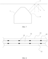
FIG. 12 is a schematic structural diagram of agglomeration of a solder layer of a solder strip of a solar cell module according to the present disclosure. - Reference signs: 1: base portion; 2: reflective portion; 3: top edge; 4: first side edge; 5: second side edge; 6: first angle; 7: second angle; 8: bottom edge; 9: third side edge; 10: fourth side edge; 11: third angle; 114: fourth angle; 12: back plate; 13: packaging glass; 14: solar cell; 15: packaging adhesive film; 16: solder strip; 17: copper substrate; 18: solder layer; 19: folded section; 20: fifth side edge; 21: sixth side edge; 22: seventh side edge; 23: eighth side edge; 24: fifth angle; 25: sixth angle.
- Embodiments described below with reference to the accompanying drawings are exemplary and intended only to illustrate the present disclosure, which cannot be construed as limitations to the present disclosure.
- As shown in
FIG. 1 and FIG. 2 , an embodiment of the present disclosure provides asolder strip 16. Thesolder strip 16 is of an elongated strip structure. Across section of thesolder strip 16 includes abase portion 1 and areflective portion 2 arranged above thebase portion 1. Thereflective portion 2 and thebase portion 1 may have an integrated structure, and the division into two parts is only for functional description. Thereflective portion 2 includes atop edge 3, afirst side edge 4 and asecond side edge 5. One end of thefirst side edge 4 and one end of thesecond side edge 5 continue from thetop edge 3. The other end of thefirst side edge 4 and the other end of thesecond side edge 5 continue from thebase portion 1. Afirst angle 6 is formed between thefirst side edge 4 and an extension line of abottom edge 8 of thebase portion 1, asecond angle 7 is formed between thesecond side edge 5 and the extension line of thebottom edge 8 of thebase portion 1, and thefirst angle 6 and thesecond angle 7 are both greater than 42.5° and less than 90° (excluding 90°). - In the present embodiment, when the
first angle 6 and/or thesecond angle 7 are/is greater than 42.5° and less than 90°, referring toFIG. 5 , after reflected light incident on thesolder strip 16 in a direction perpendicular to thesecond side edge 5strikes packaging glass 13, an incident angle (an angle between the reflected light and a normal line of the packaging glass 13) is equal to thesecond angle 7. According to a principle of total reflection of light, the reflected light incident on thesolder strip 16 may be totally reflected at a glass and air interface layer of the solar cell module, so that the sunlight totally reflected re-participates in photoelectric conversion and thus improves the utilization of the reflected light. - In an embodiment, when the
first angle 6 and thesecond angle 7 are greater than 42.5° (42.5° is a critical angle at which the sunlight is totally reflected at a glass and air interface layer of a photovoltaic cell module), the reflected light on thesolder strip 16 may be totally reflected to asolar cell 14 to participate in photoelectric conversion after thefirst angle 6 and thesecond angle 7 are equal to or greater than the critical angle. If thefirst angle 6 and thesecond angle 7 are less than the angle, the reflected light on thesolder strip 16 cannot meet requirements on total reflection and may pass through thepackaging glass 13 of the solar cell module, and thus cannot be utilized. - Furthermore, the
first angle 6 is equal to thesecond angle 7, that is, thefirst side edge 4 and thesecond side edge 5 are arranged symmetrically with respect to a perpendicular bisector of thebottom edge 8 of thebase portion 1, which has a symmetrically distributed structure, facilitates processing and forming, and can evenly reflect the sunlight to thesolar cells 14 on two sides, so as to improve reflection efficiency. - Furthermore, if the
first angle 6 and thesecond angle 7 are between 60° and 70°, on the one hand, a purpose that thefirst angle 6 and thesecond angle 7 are greater than the critical angle at which the sunlight is totally reflected at the glass and air interface layer of the photovoltaic cell module can be achieved. On the other hand, accumulation caused by melting of asolder layer 18 during the soldering of thesolder strip 16 is also prevented, so that thicknesses of thefirst side edge 4 and thesecond side edge 5 are increased, thereby reducing thefirst angle 6 and thesecond angle 7. Thefirst angle 6 and thesecond angle 7 are both set to 60° to 70° so that a margin can be remained. In a case where thesolder layer 18 is accumulated, thefirst angle 6 and thesecond angle 7 are still greater than the critical angle at which the sunlight is totally reflected at the glass and air interface layer of the solar cell module. - Further, when the height of the cross-section of the
solder strip 16 is designed to be less than 0.3 mm, in a case where thesolder strip 16 has asame copper substrate 17 as a round-wire solder strip 16 (i.e., a same power is maintained), a weight of apackaging adhesive film 15 can be reduced due to a reduced height of thesolder strip 16, so as to reduce costs. After thesolder strip 16 is welded to thesolar cell 14, a space between thesolar cell 14 and thepackaging glass 13 may be filled with thepackaging adhesive film 15. The height of thesolder strip 16 may determine a gap between thesolar cell 14 and thepackaging glass 13. In a case where the height of thesolder strip 16 is reduced, the gap between thesolar cell 14 and thepackaging glass 13 may also be reduced, thereby reducing a volume of the filledpackaging adhesive film 15. - Furthermore, the
base portion 1 has a width of 0.4±0.1 mm and a height of 0.18±0.02 mm; and thereflective portion 2 has a height of 0.09±0.01 mm. Therefore, compared with the height, the width of thesolder strip 16 has a certain amount of expansion, which results in that the solder strip is not easily turned over during the soldering and solves the problem of difficulty in a soldering process of the triangular solder strip in the related art. - Referring to
FIG. 3 , in an example, thesolder strip 16 is 0.3 mm high and 0.41 mm wide, and is compared with a round-wire segmented soldering wire with asame copper substrate 17. - Given 0.3 mm * 0.41 mm, the height is 0.3 mm, and a low-weight adhesive film packaging material may be used compared with the solder strip with a round wire of 0.35 mm. The cost of a single adhesive film of the module can be reduced by 4-5 RMB.
- By taking a 182-72HC module as an example, due to the design of reflection, power of a T-shaped
solder strip 16 of 0.3 mm *0.41 mm may be increased by about 1 W compared with the module with a round wire of 0.35 mm. - Referring to
FIG. 4 , in an example, thesolder strip 16 is 0.27 mm high and 0.4mm wide, and is compared with a round-wire segmented soldering wire with asame copper substrate 17. - According to 0.27 mm *0.4 mm, the height is 0.27 mm, and a low-weight adhesive film packaging material may be used compared with the solder strip with a round wire of 0.35 mm. The cost of a single adhesive film of the module can be reduced by 4.3-5.3 RMB.
- By taking a 182-72HC module as an example, due to the design of reflection, power of a T-shaped
solder strip 16 of 0.27 mm *0.4 mm may be increased by about 1 W compared with the module with a round wire of 0.35 mm. - In the related art, as shown in
FIG. 11 , the solder strip has a triangular section. Although the design is intended to provide two bevel side edges as effective side edges so as to increase an effective reflective light multiplexing area, after soldering, the solder layer on the bevel side edge may be melted and agglomerate in a middle part of the bevel side edge. As a result, after the soldering, two bevel side edges of the solder strip may change from a bevel surface to an arc-like surface that protrudes in the middle. A round-wire-like surface leads to loss of reflective multiplexing capability. - In order to solve the above technical problem, the
base portion 1 further includes athird side edge 9 and afourth side edge 10, and thethird side edge 9 and thefourth side edge 10 are arranged opposite to each other. Two opposite ends of thethird side edge 9 are connected to thebottom edge 8 and thefirst side edge 4 respectively, and athird angle 11 is formed between thethird side edge 9 and thebottom edge 8. Two opposite ends of thefourth side edge 10 are connected to thebottom edge 8 and thesecond side edge 5, respectively, and a fourth angle 114 is formed between thefourth side edge 10 and thebottom edge 8. Thethird angle 11 and the fourth angle 114 may be right angles, so as to form a structure with an isosceles trapezoid at a top and a rectangle at a bottom, which meets requirements on light reflection, unlike thetriangular solder strip 16, this will prevent agglomeration of thesolder layer 18 after soldering of the bevel side edge. As shown inFIG. 12 , an agglomeration layer is formed between thebase portion 1 and thesolar cell 14. Thesolder layer 18 slides to the bottom, while thesolder layer 18 does not agglomerate at the bevel side edge, which brings a good light reflection effect. - Further, the
third angle 11 and the fourth angle 114 are obtuse angles, and may be 120°. That is, thethird side edge 9 and thefourth side edge 10 gradually tilt inward from top to bottom to form a rhomboid structure. After the soldering, since thethird side edge 9 and thefourth side edge 10 tilt inward, thethird side edge 9 and thefourth side edge 10 form an accommodating space with the top of thesolar cell 14 compared with the design of the rectangular structure of the base portion. Therefore, after the soldering, thesolder layer 18 slides from thefirst side edge 4 and thesecond side edge 5 to accumulate in the accommodating space, thereby reducing the shielding of a surface of thesolar cell 14. - The
solder strip 16 includes acopper substrate 17 and asolder layer 18 coated on a surface of thecopper substrate 17. Thecopper substrate 17 is made of pure copper, oxygen-free copper or red copper, and thesolder layer 18 is made of pure tin, a tin-lead mixture or a tin-lead-silver mixture. Thecopper substrate 17 is configured for current transmission, and thesolder layer 18 is configured for soldering with a gate line on the surface of thesolar cell 14. A thickness of thesolder layer 18 is controlled at 10 µm and 15 µm, which is uniformly coated on thecopper substrate 17. - Amain difference between the present embodiment and
Embodiment 1 is as follows. InEmbodiment 1, thefirst side edge 4 and/or thesecond side edge 5 is an approximately smooth surface, and reflected light is at a single angle and has a limited coverage. In the present embodiment, referring toFIG. 6 andFIG. 7 , thefirst side edge 4 and/or thesecond side edge 5 include/includes a plurality of continuous foldedsections 19. Angles between the plurality of continuous foldedsections 19 and the extension line of thebottom edge 8 of thebase portion 1 are greater than the preset angle. In this way, each foldedsection 19 reflects sunlight at different angles, thereby improving the coverage of the sunlight that re-participates in photoelectric conversion. - Referring to
FIG. 7 , after reflected light on thesolder strip 16 perpendicular to the foldedsection 19 strikes thepackaging glass 13, an incident angle (an angle between the reflected light and a normal line of the packaging glass 13) is equal to thesecond angle 7. According to the principle of total reflection of light, the reflected light on thesolder strip 16 may be totally reflected at a glass and air interface layer of the solar cell module, so that the sunlight totally reflected re-participates in photoelectric conversion and thus improves the utilization of the reflected light. - Furthermore, the angle between the folded
section 19 and the extension line of thebottom edge 8 of thebase portion 1 increases sequentially from top to bottom to form a progressively inclined surface with a certain gradient, so that the solder layer can slide down along each foldedsection 19 during melting, so as not to produce agglomeration on thefirst side edge 4 and/or thesecond side edge 5 to adversely affect the light reflection effect and reduce the utilization of the sunlight. - The present disclosure further provides a solar cell module. Referring to
FIG. 8 andFIG. 9 , the solar cell module includessolar cells 14 and thesolder strip 16 described above. Thebase portion 1 of thesolder strip 16 is welded to thesolar cells 14. Adjacentsolar cells 14 are electrically connected to each other through thesolder strip 16, and a current is transmitted by thesolder strip 16. - Referring to
FIG. 10 , a cross section of thesolder strip 16 includes abase portion 1 and areflective portion 2 arranged above thebase portion 1. Thereflective portion 2 includes atop edge 3, afifth side edge 20 and asixth side edge 21. Due to solder melting of the solder layer 18 (especially at a position near a soldering spot) of thesolder strip 16 during the soldering, a certain flow accumulation occurs, resulting in slightly protruding arc-surface structures of thefifth side edge 20 and thesixth side edge 21. At the same time, thetop edge 3 may also be an arc-surface structure, which is connected to thefifth side edge 20 and thesixth side edge 21. One end of thefifth side edge 20 and one end of thesixth side edge 21 continue from thetop edge 3. The other end of thefifth side edge 20 and the other end of thesixth side edge 21 continue from thebase portion 1. Afifth angle 24 is formed between a tangent line of thefifth side edge 20 and an extension line of a bottom edge of thebase portion 1. Asixth angle 25 is formed between a tangent line of thesixth side edge 21 and the extension line of the bottom edge of thebase portion 1. The tangent lines of thefifth side edge 20 and thesixth side edge 21 are tangent lines of the farthest point of a convex arc surface. Thefifth angle 24 and thesixth angle 25 are between 42.5° and 90° (excluding 90°). - After the soldering of the
solder strip 16, thesolder layer 18 melts, and thefifth side edge 20 and thesixth side edge 21 form a convex arc-surface structure. Angles between tangent lines of midpoints of thefifth side edge 20 and thesixth side edge 21 and the extension line of thebottom edge 8 of thebase portion 1 are greater than 42.5°. The midpoints of thefifth side edge 20 and thesixth side edge 21 are located at most protruding points of the arc-surface structure. In an embodiment, the midpoint is in the middle of the arc-surface structure and on thesolder strip 16. After reflected light incident in a direction perpendicular to thefifth side edge 20 and thesixth side edge 21 strikes thepackaging glass 13, an incident angle (an angle between the reflected light and a normal line of the packaging glass 13) is equal to thefifth angle 24 and thesixth angle 25. According to the principle of total reflection of light, the reflected light on thesolder strip 16 may be totally reflected at a glass and air interface layer of the solar cell module, so that the sunlight totally reflected re-participates in photoelectric conversion and thus improves the utilization of the reflected light. - Furthermore, the
solder strip 16 includes a main body section and a flat section. The main body section is configured to be welded to a busbar of thesolar cell 14. The flat section is located between two adjacentsolar cells 14, which eliminates spacing between solar cells and increases power of the module per unit area. The flat section in the middle reduces a vertical spacing between thesolar cells 14, reduces ethylene vinyl acetate (EVA) consumption, reduces hidden cracks, and improves the reliability of a photovoltaic module. - Further, the flat section is of a flat elongated strip structure, and a bottom edge of the flat section is parallel to that of the base portion, so as to prevent turnover of the solder strip during the soldering.
- The solar cell module further includes
packaging glass 13 and aback plate 12. Theback plate 12 is arranged below thesolar cell 14. Thepackaging glass 13 is located above thesolar cell 14. A space between thepackaging glass 13 and thesolar cell 14 is filled with apackaging adhesive film 15. - Furthermore, the
base portion 1 further includes aseventh side edge 22 and aneighth side edge 23, and theseventh side edge 22 and theeighth side edge 23 are arranged opposite to each other. Two opposite ends of theseventh side edge 22 are connected to thebottom edge 8 and thefifth side edge 20 respectively, two opposite ends of theeighth side edge 23 are connected to thebottom edge 8 and thesixth side edge 21 respectively, and arc-surface transition is formed between theseventh side edge 22 and thebottom edge 8 and between theeighth side edge 23 and thebottom edge 8. - Since arc-surface transition is formed between the
seventh side edge 22 and thebottom edge 8 and between theeighth side edge 23 and thebottom edge 8, the design of fillet is increased compared with the rectangular base portion, which is conducive to the accumulation of thesolder layer 18 at the bottom of thesolder strip 16 and helps to reduce collision damages to thesolar cell 14. - Furthermore, if the
fifth angle 24 and thesixth angle 25 are between 60° and 70°, on the one hand, a purpose that thefifth angle 24 and thesixth angle 25 are greater than the critical angle at which the sunlight is totally reflected at the glass and air interface layer of the photovoltaic cell module can be achieved. On the other hand, accumulation caused by melting of asolder layer 18 during the soldering of thesolder strip 16 is also prevented, so that thicknesses of thefifth side edge 20 and thesixth side edge 21 are increased, thereby reducing thefifth angle 24 and thesixth angle 25. Thefifth angle 24 and thesixth angle 25 are both set to 60° to 70° so that a margin can be remained. In a case where thesolder layer 18 is accumulated, thefifth angle 24 and thesixth angle 25 are still greater than the critical angle at which the sunlight is totally reflected at the glass and air interface layer of the solar cell module. - Further, when the height of the cross-section of the
solder strip 16 is designed to be less than 0.3 mm, in the case of asame copper substrate 17 with a round-wire solder strip 16 (i.e. a same power is maintained), the weight of apackaging adhesive film 15 can be reduced due to a reduced height of thesolder strip 16, so as to reduce costs. After thesolder strip 16 is welded to thesolar cell 14, a space between thesolar cell 14 and thepackaging glass 13 may be filled with thepackaging adhesive film 15. The height of thesolder strip 16 may determine a gap between thesolar cell 14 and thepackaging glass 13. In a case where the height of thesolder strip 16 is reduced, the gap between thesolar cell 14 and thepackaging glass 13 may also be reduced, thereby reducing a volume of the filledpackaging adhesive film 15. - Furthermore, the
base portion 1 has a width of 0.4±0.1 mm and a height of 0.18±0.02 mm; and thereflective portion 2 has a height of 0.09±0.01 mm. Therefore, compared with the height, the width of thesolder strip 16 has a certain amount of expansion, which is easily turned over during soldering and solves the problem of difficulty in a soldering process of the triangular solder strip in the related art. After the soldering of thesolder strip 16, as shown inFIG. 12 , an agglomeration layer is formed between thebase portion 1 and thesolar cell 14. Thesolder layer 18 slides to the bottom, thesolder layer 18 does not agglomerate at a bevel side edge of a trapezoidal structure of thesolder strip 16, and thesolder layer 18 of thesolder strip 16 agglomerates only at the bottom of thebase portion 1, thereby bringing a good light reflection effect. - The structure, features and effects of the present disclosure are described in detail above according to the embodiments shown in the drawings. The above are only preferred embodiments of the present disclosure, but the present disclosure does not limit the scope of implementation as illustrated in the drawings. Any changes made in accordance with the conception of the present disclosure, or equivalent embodiments modified as equivalent changes, which still do not exceed the scope covered by the specification and the drawings, shall fall within the protection scope of the present disclosure.
Claims (15)
- A solder strip, comprising a flat section and a main body section connected to each other, wherein a cross section of the main body section comprises a base portion and a reflective portion arranged above the base portion,the reflective portion includes a top edge, a first side edge and a second side edge, one end of the first side edge and one end of the second side edge continue from the top edge, and the other end of the first side edge and the other end of the second side edge continue from the base portion, anda first angle is formed between the first side edge and an extension line of a bottom edge of the base portion, a second angle is formed between the second side edge and the extension line of the bottom edge of the base portion, and the first angle and the second angle are both acute angles formed in a range greater than 42.5°wherein the main body section comprises a substrate and a solder layer coated on a surface of the substrate, and an agglomeration formed by molten accumulation of the solder layer is located lower at two sides of the base portion.
- The solder strip according to claim 1, wherein the bottom of the base portion is chamfered or beveled to accommodate the agglomeration.
- The solder strip according to claim 1, wherein the flat section is of a flat elongated strip structure, and a bottom edge of the flat section is parallel to the bottom edge of the base portion.
- The solder strip according to claim 1, wherein the first angle and the second angle are formed in a range between 60° and 70°.
- The solder strip according to claim 1, wherein the first side edge and/or the second side edge includes a plurality of continuous folded sections, and an angle between each of the plurality of continuous folded sections and the extension line of the bottom edge of the base portion is an acute angles formed in a range greater than 42.5°.
- The solder strip according to claim 1, wherein a height of the cross-section of the solder strip is within a range of 60% to 80% of a width of the cross-section.
- The solder strip according to claim 6, wherein the height of the cross-section of the solder strip is less than or equal to 0.3 mm, the base portion has a width of 0.4±0.1 mm and a height of 0.18±0.02 mm, and the reflective portion has a height of 0.09±0.01 mm.
- The solder strip according to claim 7, the base portion has a width of 0.41 mm and a height of 0.2 mm or a width of 0.4 mm and a height of 0.17 mm, and the reflective portion has a height of 0.1 mm.
- The solder strip according to claim 1, wherein the base portion further comprises a third side edge and a fourth side edge, and the third side edge and the fourth side edge are arranged opposite to each other,wherein two opposite ends of the third side edge are connected to the bottom edge and the first side edge, respectively, and a third angle is formed between the third side edge and the bottom edge;two opposite ends of the fourth side edge are connected to the bottom edge and the second side edge, respectively, and a fourth angle is formed between the fourth side edge and the bottom edge; andthe third angle and the fourth angle are formed in a range between 90° and 120°.
- The solder strip according to claim 1, wherein
the substrate is made of pure copper, oxygen-free copper or red copper, and the solder layer is made of pure tin, a tin-lead mixture or a tin-lead-silver mixture. - The solder strip according to claim 10, wherein the solder layer has a thickness in a range of 10 µm to 15 µm.
- The solder strip according to claim 1, wherein the reflective portion includes a fifth side edge and a sixth side edge, the fifth side edge and the sixth side edge are each of a convex arc-surface structure, one end of the fifth side edge and one end of the sixth side edge continue from the top edge, and the other end of the fifth side edge and the other end of the sixth side edge continue from the base portion, a fifth angle is formed between a tangent line of a midpoint of the fifth side edge and an extension line of a bottom edge of the base portion, a sixth angle is formed between a tangent line of a midpoint of the sixth side edge and the extension line of the bottom edge of the base portion, and the fifth angle and the sixth angle are both acute angles formed in a range greater than 42.5°.
- The solder strip according to claim 1, wherein the base portion further includes a seventh side edge and an eighth side edge, the seventh side edge and the eighth side edge being arranged opposite to each other,
wherein two opposite ends of the seventh side edge are connected to the bottom edge and the fifth side edge, respectively, two opposite ends of the eighth side edge are connected to the bottom edge and the sixth side edge respectively, and an arc-surface transition is formed between the seventh side edge and the bottom edge and between the eighth side edge and the bottom edge. - A solar cell module, characterized in that, comprising a back plate, packaging glass and a plurality of solar cells according to any one of claims 1-13, wherein adjacent solar cells of the plurality of solar cells are electrically connected through a solder strip, the back plate is arranged below the plurality of solar cells, the packaging glass is located above the plurality of solar cells, and a space between the back plate and the plurality of solar cells and a space between the packaging glass and the plurality of solar cells are filled with a packaging adhesive film.
- The solar cell module according to claim 14, wherein the main body section is welded to a busbar of the plurality of solar cells, and the flat section is located between two of the plurality of solar cells.
Applications Claiming Priority (2)
| Application Number | Priority Date | Filing Date | Title |
|---|---|---|---|
| CN202110980119.XA CN113707738B (en) | 2021-08-25 | 2021-08-25 | A welding strip and a battery cell assembly |
| EP21199907.3A EP4141970B1 (en) | 2021-08-25 | 2021-09-29 | Solder strip and solar cell module |
Related Parent Applications (2)
| Application Number | Title | Priority Date | Filing Date |
|---|---|---|---|
| EP21199907.3A Division-Into EP4141970B1 (en) | 2021-08-25 | 2021-09-29 | Solder strip and solar cell module |
| EP21199907.3A Division EP4141970B1 (en) | 2021-08-25 | 2021-09-29 | Solder strip and solar cell module |
Publications (2)
| Publication Number | Publication Date |
|---|---|
| EP4266381A2 true EP4266381A2 (en) | 2023-10-25 |
| EP4266381A3 EP4266381A3 (en) | 2023-12-27 |
Family
ID=78085450
Family Applications (2)
| Application Number | Title | Priority Date | Filing Date |
|---|---|---|---|
| EP21199907.3A Active EP4141970B1 (en) | 2021-08-25 | 2021-09-29 | Solder strip and solar cell module |
| EP23196698.7A Pending EP4266381A3 (en) | 2021-08-25 | 2021-09-29 | Solder strip and solar cell module |
Family Applications Before (1)
| Application Number | Title | Priority Date | Filing Date |
|---|---|---|---|
| EP21199907.3A Active EP4141970B1 (en) | 2021-08-25 | 2021-09-29 | Solder strip and solar cell module |
Country Status (5)
| Country | Link |
|---|---|
| US (1) | US12074238B2 (en) |
| EP (2) | EP4141970B1 (en) |
| JP (1) | JP7223092B1 (en) |
| CN (1) | CN113707738B (en) |
| AU (2) | AU2021240257B2 (en) |
Family Cites Families (35)
| Publication number | Priority date | Publication date | Assignee | Title |
|---|---|---|---|---|
| US5266125A (en) * | 1992-05-12 | 1993-11-30 | Astropower, Inc. | Interconnected silicon film solar cell array |
| DE102004013833B4 (en) * | 2003-03-17 | 2010-12-02 | Kyocera Corp. | Method for producing a solar cell module |
| EP2214213A2 (en) * | 2009-01-29 | 2010-08-04 | SCHOTT Solar AG | Photovoltaic module |
| CN102347375A (en) * | 2010-07-30 | 2012-02-08 | E·I·内穆尔杜邦公司 | Solar battery module comprising conductive bands covering reflection strips |
| CN102201471B (en) * | 2011-04-20 | 2012-11-28 | 昆明三利特科技有限责任公司 | Photovoltaic interconnector for absorbing stress |
| DE102011053238A1 (en) * | 2011-09-02 | 2013-03-07 | Schott Solar Ag | Method for connecting solar cells and solar cell module |
| CN103022170A (en) * | 2012-12-29 | 2013-04-03 | 常州大学 | Reflective strip of photovoltaic module and method for implementing reflective strip |
| CN203812889U (en) * | 2014-03-10 | 2014-09-03 | 余小翠 | Solar cell with reflectors |
| CN105374885B (en) * | 2014-09-29 | 2017-04-12 | 凡登(江苏)新型材料有限公司 | Manufacturing method and production line of heterogeneous high-efficiency photovoltaic solder strip and conductive base band |
| CN104319314A (en) * | 2014-10-28 | 2015-01-28 | 云飞 | Preparing technology of photovoltaic cell |
| CN106158993B (en) * | 2016-08-26 | 2017-07-14 | 江苏东鋆光伏科技有限公司 | Cell piece point-like main gate line interconnects reflective battery component and preparation method thereof |
| CN106784102A (en) * | 2017-01-12 | 2017-05-31 | 保定易通光伏科技股份有限公司 | Photovoltaic welding belt and photovoltaic module |
| CN207320132U (en) * | 2017-10-16 | 2018-05-04 | 浙江昱辉阳光能源江苏有限公司 | A kind of high CTM high simultaneously hinders efficient photovoltaic module |
| KR20190089709A (en) * | 2018-01-22 | 2019-07-31 | 엘지전자 주식회사 | Solar cell module |
| EP3544062A1 (en) * | 2018-03-22 | 2019-09-25 | LG Electronics Inc. | Interconnecting member for solar cell panel and solar cell panel including the same |
| CN208045523U (en) | 2018-04-18 | 2018-11-02 | 刘岩岩 | A kind of connection structure of low resistance type reflective solder strip |
| CN108767046B (en) * | 2018-07-31 | 2024-03-01 | 无锡奥特维科技股份有限公司 | Photovoltaic solder strip, manufacturing method, solar cell string and solar cell module |
| CN111261742A (en) * | 2018-12-17 | 2020-06-09 | 宁波森联光电科技有限公司 | Photovoltaic device and photovoltaic solder strip and method of manufacturing the same |
| CN211700308U (en) | 2018-12-17 | 2020-10-16 | 宁波森联光电科技有限公司 | Photovoltaic device and photovoltaic solder strip |
| WO2020220094A1 (en) * | 2019-05-02 | 2020-11-05 | Newsouth Innovations Pty Limited | A method of forming a device structure |
| CN114051659B (en) * | 2019-05-02 | 2025-08-29 | 隆基绿能科技股份有限公司 | Structured connectors for interconnecting device components |
| CN210156392U (en) * | 2019-07-30 | 2020-03-17 | 宁波森联光电科技有限公司 | High-efficient photovoltaic module |
| CN210272398U (en) * | 2019-08-21 | 2020-04-07 | 泰州隆基乐叶光伏科技有限公司 | Welding strip for photovoltaic module |
| CN110518077A (en) * | 2019-08-30 | 2019-11-29 | 苏州阿特斯阳光电力科技有限公司 | A kind of solar battery sheet and photovoltaic module |
| CN110783422A (en) * | 2019-11-20 | 2020-02-11 | 凡登(江苏)新型材料有限公司 | High-efficient photovoltaic solder strip |
| CN210640262U (en) * | 2019-11-20 | 2020-05-29 | 凡登(江苏)新型材料有限公司 | High Efficiency Photovoltaic Ribbon |
| CN210837788U (en) * | 2019-11-29 | 2020-06-23 | 英利能源(中国)有限公司 | Reflection of light solder strip and photovoltaic module |
| CN111223953A (en) | 2019-11-29 | 2020-06-02 | 英利能源(中国)有限公司 | A kind of reflective welding tape, photovoltaic module and preparation method |
| CN211555908U (en) * | 2020-01-19 | 2020-09-22 | 宁波林源光电科技有限公司 | Reflective welding strip |
| CN111446321A (en) * | 2020-01-20 | 2020-07-24 | 宁波森联光电科技有限公司 | Conductive tape, photovoltaic device and application |
| CN111192933A (en) * | 2020-03-08 | 2020-05-22 | 上海金羊钫新能源科技中心(有限合伙) | A solar photovoltaic component and a building photovoltaic integrated component |
| CN211957663U (en) * | 2020-06-10 | 2020-11-17 | 张彩萍 | Photovoltaic solder strip |
| CN212676286U (en) * | 2020-09-30 | 2021-03-09 | 江苏东鋆光伏科技有限公司 | Multi-main-grid battery assembly with light reflecting adhesive film |
| CN212676287U (en) * | 2020-09-30 | 2021-03-09 | 江苏东鋆光伏科技有限公司 | Multi-main-grid battery piece assembly |
| CN112466974A (en) * | 2020-11-12 | 2021-03-09 | 江苏揽鑫新能源科技有限公司 | Graphene interlayer welding strip |
-
2021
- 2021-08-25 CN CN202110980119.XA patent/CN113707738B/en active Active
- 2021-09-29 EP EP21199907.3A patent/EP4141970B1/en active Active
- 2021-09-29 US US17/489,543 patent/US12074238B2/en active Active
- 2021-09-29 JP JP2021159500A patent/JP7223092B1/en active Active
- 2021-09-29 EP EP23196698.7A patent/EP4266381A3/en active Pending
- 2021-09-30 AU AU2021240257A patent/AU2021240257B2/en active Active
-
2023
- 2023-09-15 AU AU2023229580A patent/AU2023229580B2/en active Active
Also Published As
| Publication number | Publication date |
|---|---|
| EP4141970B1 (en) | 2023-11-08 |
| EP4266381A3 (en) | 2023-12-27 |
| AU2023229580B2 (en) | 2025-08-14 |
| JP7223092B1 (en) | 2023-02-15 |
| US12074238B2 (en) | 2024-08-27 |
| EP4141970A1 (en) | 2023-03-01 |
| US20230066924A1 (en) | 2023-03-02 |
| AU2023229580A1 (en) | 2023-10-05 |
| CN113707738B (en) | 2025-03-21 |
| CN113707738A (en) | 2021-11-26 |
| AU2021240257A1 (en) | 2023-03-16 |
| AU2021240257B2 (en) | 2023-08-03 |
| JP2023033039A (en) | 2023-03-09 |
Similar Documents
| Publication | Publication Date | Title |
|---|---|---|
| EP4557378A1 (en) | Photovoltaic cell unit and preparation methods therefor | |
| EP4386870A1 (en) | Photovoltaic module | |
| US20250081665A1 (en) | Solar cell and photovoltaic module | |
| WO2022193578A1 (en) | Solar cell connecting method | |
| CN214123892U (en) | Solar cell and photovoltaic module | |
| CN115763603A (en) | Photovoltaic module | |
| AU2023309075A1 (en) | Photovoltaic shingled module and manufacturing method therefor | |
| JP7676598B2 (en) | Photovoltaic module and method of manufacturing same | |
| CN215183991U (en) | Battery piece and photovoltaic module with same | |
| US12074238B2 (en) | Solder strip and solar cell module | |
| CN223810093U (en) | A solar cell and photovoltaic module | |
| CN108461559A (en) | The two-sided photovoltaic stacked wafer moudle that compatible terminal box is blocked | |
| CN219226307U (en) | Segmented structure welding strip and photovoltaic module | |
| CN213459762U (en) | Photovoltaic solder strip and photovoltaic module | |
| WO2024087506A1 (en) | Solder strip and preparation method therefor, and photovoltaic module | |
| US20150144175A1 (en) | Photovoltaic module with photovoltaic cells having local widening of the bus | |
| CN209896086U (en) | A kind of reflective welding tape for photovoltaic modules and photovoltaic modules | |
| AU2023254873A1 (en) | Solar cell and photovoltaic module | |
| CN115775838A (en) | Photovoltaic module and preparation method | |
| CN223652632U (en) | Photovoltaic modules and their reflective busbars | |
| CN115602744A (en) | Solar cell and photovoltaic module | |
| CN223829707U (en) | A photovoltaic welding strip | |
| CN222621522U (en) | Solar cells and photovoltaic modules | |
| CN222721917U (en) | Grid line electrode of photovoltaic cell, photovoltaic cell and photovoltaic module | |
| CN218513467U (en) | Photovoltaic module |
Legal Events
| Date | Code | Title | Description |
|---|---|---|---|
| PUAI | Public reference made under article 153(3) epc to a published international application that has entered the european phase |
Free format text: ORIGINAL CODE: 0009012 |
|
| STAA | Information on the status of an ep patent application or granted ep patent |
Free format text: STATUS: THE APPLICATION HAS BEEN PUBLISHED |
|
| AC | Divisional application: reference to earlier application |
Ref document number: 4141970 Country of ref document: EP Kind code of ref document: P |
|
| AK | Designated contracting states |
Kind code of ref document: A2 Designated state(s): AL AT BE BG CH CY CZ DE DK EE ES FI FR GB GR HR HU IE IS IT LI LT LU LV MC MK MT NL NO PL PT RO RS SE SI SK SM TR |
|
| PUAL | Search report despatched |
Free format text: ORIGINAL CODE: 0009013 |
|
| AK | Designated contracting states |
Kind code of ref document: A3 Designated state(s): AL AT BE BG CH CY CZ DE DK EE ES FI FR GB GR HR HU IE IS IT LI LT LU LV MC MK MT NL NO PL PT RO RS SE SI SK SM TR |
|
| RIC1 | Information provided on ipc code assigned before grant |
Ipc: H01L 31/05 20140101AFI20231123BHEP |
|
| STAA | Information on the status of an ep patent application or granted ep patent |
Free format text: STATUS: REQUEST FOR EXAMINATION WAS MADE |
|
| 17P | Request for examination filed |
Effective date: 20240624 |
|
| RBV | Designated contracting states (corrected) |
Designated state(s): AL AT BE BG CH CY CZ DE DK EE ES FI FR GB GR HR HU IE IS IT LI LT LU LV MC MK MT NL NO PL PT RO RS SE SI SK SM TR |
|
| STAA | Information on the status of an ep patent application or granted ep patent |
Free format text: STATUS: EXAMINATION IS IN PROGRESS |
|
| 17Q | First examination report despatched |
Effective date: 20250915 |