EP4266154A1 - Protection method, protection apparatus, electronic device, readable storage medium, and chip - Google Patents
Protection method, protection apparatus, electronic device, readable storage medium, and chip Download PDFInfo
- Publication number
- EP4266154A1 EP4266154A1 EP21905588.6A EP21905588A EP4266154A1 EP 4266154 A1 EP4266154 A1 EP 4266154A1 EP 21905588 A EP21905588 A EP 21905588A EP 4266154 A1 EP4266154 A1 EP 4266154A1
- Authority
- EP
- European Patent Office
- Prior art keywords
- pin
- configuration channel
- universal serial
- serial bus
- bus interface
- Prior art date
- Legal status (The legal status is an assumption and is not a legal conclusion. Google has not performed a legal analysis and makes no representation as to the accuracy of the status listed.)
- Granted
Links
Images


Classifications
-
- G—PHYSICS
- G06—COMPUTING OR CALCULATING; COUNTING
- G06F—ELECTRIC DIGITAL DATA PROCESSING
- G06F13/00—Interconnection of, or transfer of information or other signals between, memories, input/output devices or central processing units
- G06F13/38—Information transfer, e.g. on bus
- G06F13/40—Bus structure
- G06F13/4063—Device-to-bus coupling
- G06F13/4068—Electrical coupling
- G06F13/4081—Live connection to bus, e.g. hot-plugging
-
- G—PHYSICS
- G06—COMPUTING OR CALCULATING; COUNTING
- G06F—ELECTRIC DIGITAL DATA PROCESSING
- G06F13/00—Interconnection of, or transfer of information or other signals between, memories, input/output devices or central processing units
- G06F13/38—Information transfer, e.g. on bus
- G06F13/40—Bus structure
- G06F13/4063—Device-to-bus coupling
- G06F13/4068—Electrical coupling
-
- G—PHYSICS
- G06—COMPUTING OR CALCULATING; COUNTING
- G06F—ELECTRIC DIGITAL DATA PROCESSING
- G06F1/00—Details not covered by groups G06F3/00 - G06F13/00 and G06F21/00
- G06F1/26—Power supply means, e.g. regulation thereof
- G06F1/266—Arrangements to supply power to external peripherals either directly from the computer or under computer control, e.g. supply of power through the communication port, computer controlled power-strips
-
- G—PHYSICS
- G06—COMPUTING OR CALCULATING; COUNTING
- G06F—ELECTRIC DIGITAL DATA PROCESSING
- G06F13/00—Interconnection of, or transfer of information or other signals between, memories, input/output devices or central processing units
- G06F13/38—Information transfer, e.g. on bus
- G06F13/382—Information transfer, e.g. on bus using universal interface adapter
- G06F13/385—Information transfer, e.g. on bus using universal interface adapter for adaptation of a particular data processing system to different peripheral devices
-
- G—PHYSICS
- G06—COMPUTING OR CALCULATING; COUNTING
- G06F—ELECTRIC DIGITAL DATA PROCESSING
- G06F13/00—Interconnection of, or transfer of information or other signals between, memories, input/output devices or central processing units
- G06F13/38—Information transfer, e.g. on bus
- G06F13/42—Bus transfer protocol, e.g. handshake; Synchronisation
- G06F13/4282—Bus transfer protocol, e.g. handshake; Synchronisation on a serial bus, e.g. I2C bus, SPI bus
-
- H—ELECTRICITY
- H02—GENERATION; CONVERSION OR DISTRIBUTION OF ELECTRIC POWER
- H02H—EMERGENCY PROTECTIVE CIRCUIT ARRANGEMENTS
- H02H3/00—Emergency protective circuit arrangements for automatic disconnection directly responsive to an undesired change from normal electric working condition with or without subsequent reconnection ; integrated protection
- H02H3/20—Emergency protective circuit arrangements for automatic disconnection directly responsive to an undesired change from normal electric working condition with or without subsequent reconnection ; integrated protection responsive to excess voltage
- H02H3/202—Emergency protective circuit arrangements for automatic disconnection directly responsive to an undesired change from normal electric working condition with or without subsequent reconnection ; integrated protection responsive to excess voltage for DC systems
-
- G—PHYSICS
- G06—COMPUTING OR CALCULATING; COUNTING
- G06F—ELECTRIC DIGITAL DATA PROCESSING
- G06F2213/00—Indexing scheme relating to interconnection of, or transfer of information or other signals between, memories, input/output devices or central processing units
- G06F2213/0002—Serial port, e.g. RS232C
-
- G—PHYSICS
- G06—COMPUTING OR CALCULATING; COUNTING
- G06F—ELECTRIC DIGITAL DATA PROCESSING
- G06F2213/00—Indexing scheme relating to interconnection of, or transfer of information or other signals between, memories, input/output devices or central processing units
- G06F2213/0042—Universal serial bus [USB]
-
- Y—GENERAL TAGGING OF NEW TECHNOLOGICAL DEVELOPMENTS; GENERAL TAGGING OF CROSS-SECTIONAL TECHNOLOGIES SPANNING OVER SEVERAL SECTIONS OF THE IPC; TECHNICAL SUBJECTS COVERED BY FORMER USPC CROSS-REFERENCE ART COLLECTIONS [XRACs] AND DIGESTS
- Y02—TECHNOLOGIES OR APPLICATIONS FOR MITIGATION OR ADAPTATION AGAINST CLIMATE CHANGE
- Y02D—CLIMATE CHANGE MITIGATION TECHNOLOGIES IN INFORMATION AND COMMUNICATION TECHNOLOGIES [ICT], I.E. INFORMATION AND COMMUNICATION TECHNOLOGIES AIMING AT THE REDUCTION OF THEIR OWN ENERGY USE
- Y02D10/00—Energy efficient computing, e.g. low power processors, power management or thermal management
Definitions
- This application pertains to the technical field of electronic data transmission, and in particular, to a universal serial bus interface protection method, a universal serial bus interface protection apparatus, an electronic device, a readable storage medium, and a chip.
- An on-the-go (OTG) device that uses a universal serial bus (Universal Serial Bus, USB) interface technology may implement communication connections and data exchange between multiple different terminal devices, and in particular, implement connections of multiple different standards between devices such as a personal digital assistant (Personal Digital Assistant, PDA) device, a smartphone, a digital camera, a camera, and a printer.
- PDA Personal Digital Assistant
- the OTG device may implement a connection between slave devices without a master device.
- a Type-C universal serial bus interface has a wide application prospect in the OTG device due to advantages of being pluggable on both sides and being small in size.
- an OTG device with the Type-C universal serial bus interface has at least the following problems in a related technology.
- a configuration channel (Configuration Channel, CC) pin of the Type-C universal serial bus interface needs to be in a constantly charged state, to detect a type of an inserted device.
- the configuration channel pin in the charged state is vulnerable to corrosion or damage due to a short circuit, and consequently, a service life of the Type-C universal serial bus interface is affected.
- Embodiments of this application are to provide a universal serial bus interface protection method, a universal serial bus interface protection apparatus, an electronic device, a readable storage medium, and a chip, which can resolve a problem that a Type-C universal serial bus interface is vulnerable to corrosion or damage due to a short circuit.
- an embodiment of this application provides a universal serial bus interface protection method, where a configuration channel pin is disposed on a universal serial bus interface, and the protection method includes: detecting a voltage variable of the configuration channel pin; determining conversion time of the voltage variable according to the voltage variable; comparing the conversion time with preset conversion time to obtain a comparison result; and cutting off power supply of the configuration channel pin in a case that the comparison result is that the conversion time is less than or equal to preset conversion time,.
- an embodiment of this application provides a universal serial bus interface protection apparatus, where a configuration channel pin is disposed on a universal serial bus interface, and the protection apparatus includes: a detection module, where the detection module is configured to detect a voltage variable of the configuration channel pin; a determining module, where the determining module is configured to determine conversion time of the voltage variable according to the voltage variable; a comparison module, where the comparison module is configured to compare the conversion time with preset conversion time to obtain a comparison result; and a protection module, where in a case that the comparison result is that the conversion time is less than or equal to the preset conversion time, the protection module is configured to cut off power supply of the configuration channel pin.
- an embodiment of this application provides an electronic device.
- the electronic device includes a processor, a memory, and a program or an instruction that is stored in the memory and executable on the processor, and when the program or the instruction is executed by the processor, steps in the universal serial bus interface protection method according to the first aspect are implemented.
- an embodiment of this application provides a readable storage medium.
- the readable storage medium stores a program or an instruction, and the program or the instruction is executed by a processor to implement steps in the universal serial bus interface protection method according to the first aspect.
- an embodiment of this application provides a chip.
- the chip includes a processor and a communication interface, the communication interface is coupled to the processor, and the processor is configured to run a program or an instruction to implement steps in the universal serial bus interface protection method according to the first aspect.
- a state of the configuration channel pin can be accurately determined according to the voltage of the configuration channel pin. Therefore, in the embodiments of this application, a short circuit or abnormality of the configuration channel pin caused when a foreign object enters a universal serial bus interface can be identified in time, and power supply of the configuration channel pin can be cut off in time, to avoid corrosion or damage of the configuration channel pin. In conclusion, in the embodiments of this application, the universal serial bus interface can be effectively protected, and a service life of the universal serial bus interface can be improved.
- FIG. 1, FIG. 2 , FIG. 4 to FIG. 6 , and FIG. 8 are as follows: A1: Upper-row first pin; A2: Upper-row second pin; A3: Upper-row third pin; A4: Upper-row fourth pin; A5: Upper-row fifth pin; A6: Upper-row sixth pin; A7: Upper-row seventh pin; A8: Upper-row eighth pin; A9: Upper-row ninth pin; A10: Upper-row tenth pin; A11: Upper-row eleventh pin; A12: Upper-row twelfth pin; B1: Lower-row first pin; B2: Lower-row second pin; B3: Lower-row third pin; B4: Lower-row fourth pin; B5: Lower-row fifth pin; B6: Lower-row sixth pin; B7: Lower-row seventh pin; B8: Lower-row eighth pin; B9: Lower-row ninth pin; B10: Lower-row tenth pin; B11: Lower-row eleventh pin;
- the protection method provided in the embodiments of this application is a protection method for a Type-C universal serial bus interface.
- the Type-C universal serial bus interface includes a Type-C universal serial bus interface of a socket and a Type-C universal serial bus interface of a plug.
- a pin arrangement manner of the Type-C universal serial bus interface of the socket is opposite to a pin arrangement manner of the Type-C universal serial bus interface of the plug.
- the pin arrangement manner of the Type-C universal serial bus interface of the socket is used as an example to describe a pin arrangement manner of the universal serial bus interface.
- FIG. 1 is a diagram of pin arrangement of a universal serial bus interface according to an embodiment of this application.
- a Type-C universal serial bus interface has a symmetrical structure, and includes upper-row pins and lower-row pins that are disposed in an up-and-down opposite manner.
- the upper-row pins successively include an upper-row first pin A1, an upper-row second pin A2, an upper-row third pin A3, an upper-row fourth pin A4, an upper-row fifth pin A5, an upper-row sixth pin A6, an upper-row seventh pin A7, an upper-row eighth pin A8, an upper-row ninth pin A9, an upper-row tenth pin A10, an upper-row eleventh pin A11, and an upper-row twelfth pin A12 from left to right.
- the upper-row first pin A1 is a ground cable pin GND
- the upper-row second pin A2 is a first transmit+ pin TX1+
- the upper-row third pin A3 is a first transmit- pin TX1-
- the upper-row fourth pin A4 is a voltage bus pin VBus
- the upper-row fifth pin A5 is a first configuration channel pin CC1
- the upper-row sixth pin A6 is a data+ pin D+
- the upper-row seventh pin A7 is a data packet- pin D-
- the upper-row eighth pin A8 is a first extended function pin SBU1
- the upper-row ninth pin A9 is the voltage bus pin VBus
- the upper-row tenth pin A10 is a second receive- pin RX2-
- the upper-row eleventh pin A11 is a second receive+ pin RX2+
- the upper-row twelfth pin A12 is the ground cable pin GND.
- the lower-row pins successively include a lower-row first pin B1, a lower-row second pin B2, a lower-row third pin B3, a lower-row fourth pin B4, a lower-row fifth pin B5, a lower-row sixth pin B6, a lower-row seventh pin B7, a lower-row eighth pin B8, a lower-row ninth pin B9, a lower-row tenth pin B10, a lower-row eleventh pin B11, and a lower-row twelfth pin B12 from right to left.
- the lower-row first pin B1 is a ground cable pin GND
- the lower-row second pin B2 is a second transmit+ pin TX2+
- the lower-row third pin B3 is a second transmit- pin TX2-
- the lower-row fourth pin B4 is a voltage bus pin VBus
- the lower-row fifth pin B5 is a second configuration channel pin CC2
- the lower-row sixth pin B6 is a data+ pin D+
- the lower-row seventh pin B7 is a data packet- pin D-
- the lower-row eighth pin B8 is a second extended function pin SBU2
- the lower-row ninth pin B9 is the voltage bus pin VBus
- the lower-row tenth pin B10 is a first receive- pin RX1-
- the lower-row eleventh pin B11 is a first receive+ pin RX1+
- the lower-row twelfth pin B12 is the ground cable pin GND.
- both the first configuration channel pin CC1 and the second configuration channel pin CC2 are configuration channel pins, and the configuration channel pin is one of important components of a Type-C universal serial bus interface.
- the configuration channel pin is used to detect or determine a type of an inserted device.
- a principle in which the configuration channel pin implements the foregoing functions is as follows: An identification manner when the OTG device is used is: A downstream facing port (Downstream Facing Port, DFP) is primary, and an upstream facing port (Upstream Facing Port, UFP) is secondary. A dual role port (Dual Role port, DRP) may be used as a downstream facing port or an upstream facing port. When two dual role ports are connected together, either party is a downstream facing port, and the other party is an upstream facing port. There is a pull-up resistor Rp on a configuration channel pin of the downstream facing port, and there is a pull-down resistor Rd on a configuration channel pin of the upstream facing port.
- a voltage bus pin VBus of the downstream facing port has no output.
- the two configuration channel pins are connected. If the configuration channel pin of the downstream facing port detects the pull-down resistor Rd of the upstream facing port, it indicates that the devices are connected, and the downstream facing port turns on a VBus power supply and outputs power to the upstream facing port.
- the configuration channel pin includes a first configuration channel pin CC1 and a second configuration channel pin CC2. When a pull-down resistor is detected according to one of the first configuration channel pin CC1 and the second configuration channel pin CC2, a direction of interface insertion may be determined, and a transmit+ pin and a receive+ pin are switched accordingly.
- the configuration channel pin is used as an insertion detection pin, and different states (for example, ralrd/rp def/rp_15/rp 30) are entered according to an external load condition or a configuration channel state of the OTG device.
- a configuration channel state of each OTG device is stable, that is, when an OTG device is inserted, there are no two types of device identification voltages on a configuration channel.
- a configuration channel state pin voltage of a secondary (English name: Sink) OTG device is shown in Table 1 and Table 2.
- Table 1 Configure channel state pin voltage (only a USB Type-C current is preset) Detection Minimum voltage Maximum voltage Threshold voltage vRa -0.25V 0.15V 0.2V vRa-Connect 0.25V 2.18V - Table 2 Configuration channel state pin voltage (multi-element current) Detection Minimum voltage Maximum voltage Threshold voltage vRa -0.25V 0.15V 0.2V vRa-Connect 0.25V 2.04V - vRa-USB 0.25V 0.61V 0.66V vRa-1.5 0.70V 1.16V 1.23 V vRa-3.0 1.31V 2.04V -
- the configuration channel pin when used as the insertion detection element, it needs to be ensured that the configuration channel pin is in a constantly charged state.
- corrosion is caused inside the charged universal serial bus interface, especially in the charged configuration channel pin.
- This problem affects not only implementation of a common function of the universal serial bus interface, such as charging, data transmission, and screen projection, but also a service life of the universal serial bus interface. Even if there is a technical solution for reducing corrosion through coating in a related technology, an effect thereof is limited and costs are high.
- FIG. 2 is a schematic diagram of a structure of a universal serial bus interface according to an embodiment of this application.
- the upper-row pins of the Type-C universal serial bus interface in FIG. 1 are used as an example.
- the upper-row fourth pin A4 is a voltage bus pin VBus
- the upper-row fifth pin A5 is a first configuration channel pin CC1
- the upper-row sixth pin A6 is a data+ pin D+.
- the first configuration channel pin CC1 is disposed between the voltage bus pin VBus and the data+ pin D+.
- the data pin D+ supports an operating voltage of 5V
- the voltage bus pin VBus supports an operating voltage of a maximum of 20V. Therefore, when a foreign object is stuck around the first configuration channel pin CC1, the first configuration channel pin CC1 is prone to a short circuit, causing damage to an interface and a device. Therefore, an embodiment of this application provides a universal serial bus interface protection method.
- FIG. 3 is a first step flowchart of a universal serial bus interface protection method according to an embodiment of this application. As shown in FIG. 3 , based on the foregoing principle, this embodiment of this application proposes the following protection method:
- a short-circuit phenomenon may occur between a first configuration channel pin CC1 and a voltage bus pin VBus, or may occur between a first configuration channel pin CC1 and a data+ pin D+.
- a length of the voltage bus pin VBus is relatively long, a gap between the first configuration channel pin CC1 and the voltage bus pin VBus is relatively large. From a probability perspective, it is probable that there are a foreign object and a short circuit between the first configuration channel pin CC1 and the voltage bus pin VBus. Therefore, in this embodiment of this application, as an example, there is a foreign object between the first configuration channel pin CC1 and the voltage bus pin VBus, to describe the protection method in this embodiment of this application.
- FIG. 4 is a first principle diagram of a universal serial bus interface protection method according to an embodiment of this application.
- FIG. 5 is a second principle diagram of a universal serial bus interface protection method according to an embodiment of this application.
- a circuit may be equivalent to an architecture shown in FIG. 4
- a resistor R is a micro short-circuit resistor between the configuration channel pin and the voltage bus pin VBus.
- a voltage change of a configuration channel pin in a universal serial bus interface is detected by designing a hardware circuit and improving control logic, and power on/off of the configuration channel pin is controlled, to accurately identify a foreign object or an abnormal operation of the configuration channel pin, and to effectively protect, in an abnormal state, the configuration channel pin in a timely manner.
- not only corrosion of the configuration channel pin can be effectively avoided or reduced, but also a service life of the configuration channel pin can be prolonged, and plug-and-play of the universal serial bus interface can be ensured.
- a reason for using the foregoing implementation is that a saw-shaped voltage formed due to a short-circuit of the configuration channel pin not only spans device detection voltages in two or more states, but also causes the configuration channel pin to detect frequent switching of an inserted device.
- the detection result of frequent switching of the device is caused by voltage fluctuation of the configuration channel pin that is caused by the short circuit.
- the preset conversion time in the foregoing implementation is time required when a user normally switches an OTG device.
- the preset conversion time may be preset before the device is delivered from a factory.
- the determining conversion time according to the voltage variable includes: determining the conversion time according to a change period of the voltage variable.
- the determining conversion time according to the voltage variable includes: determining the conversion time according to a waveform of the voltage variable.
- FIG. 6 is a schematic diagram of a voltage change of a configuration channel pin in a short-circuit state according to an embodiment of this application. Due to the action of the resistor R and the capacitor C in FIG. 4 and FIG. 5 , the voltage of the configuration channel pin changes as shown in FIG. 6 , so that the configuration channel pin forms a saw-shaped voltage. A specific value of the voltage spans two or more types of configuration channel state identification voltages. Therefore, in this embodiment of this application, the conversion time may be determined by using a voltage change period variable or a voltage waveform variable.
- the detecting a voltage variable of the configuration channel pin specifically includes: cyclically detecting the voltage variable of the configuration channel pin in response to a power-on instruction.
- the detecting a voltage variable of the configuration channel pin specifically includes: cyclically detecting the voltage variable of the configuration channel pin in response to a screen-on instruction.
- the detecting a voltage variable of the configuration channel pin specifically includes: detecting the voltage variable of the configuration channel pin in response to a configuration channel pin detection polling instruction.
- the detecting a voltage variable of the configuration channel pin specifically includes: cyclically detecting the voltage variable of the configuration channel pin in response to a universal serial bus interface connection instruction.
- the configuration channel pin is charged in a normal state, and therefore, in this embodiment of this application, when an OTG device is powered on or is in a normal powered-on state, the voltage variable of the configuration channel pin is cyclically detected in a fixed period through polling in response to a configuration channel pin detection polling instruction sent by the OTG device, to detect or identify a short-circuit problem of the configuration channel pin in a timely manner.
- the OTG device when the OTG device receives the power-on instruction, the voltage variable of the configuration channel pin is cyclically detected in response to the power-on instruction; or in this embodiment of this application, when the OTG device receives the universal serial bus interface connection instruction, the voltage variable of the configuration channel pin is cyclically detected in response to the universal serial bus interface connection instruction.
- a corresponding terminal device screen is turned on.
- step 102 to step 106 may be cyclically performed at least twice.
- FIG. 7 is a second step flowchart of a universal serial bus interface protection method according to an embodiment of this application. As shown in FIG. 7 , the protection method in this embodiment of this application specifically includes the following steps.
- S204 Determine whether a user manually disables an OTGI device, where if a determining result is yes, S206 is performed, or if the determining result is no, S208 is performed.
- S208 Detect a configuration channel state to determine whether there is a foreign object, where if a determining result is yes, S210 is performed, or if the determining result is no, step 212 is performed.
- S210 Disable configuration channel polling, where S216 is performed again after S210 is performed.
- S212 Enable the OTG
- device implements a plug-and-play function.
- S216 Determine whether a screen of the OTG
- S218 Determine whether the user manually enables the OTG
- S220 Determine whether the screen of the OTG
- S222 Keep configuration channel polling off, where S216 is performed again after S222 is performed.
- FIG. 8 is a schematic block diagram of composition of an electronic device according to an embodiment of this application.
- an embodiment of this application further provides an electronic device 100, including a processor 120, a memory 130, and a program or an instruction that is stored in the memory 130 and executable on the processor 120.
- the program or the instruction is executed by the processor 120, processes of the embodiments of the universal serial bus interface protection method can be implemented, and a same technical effect can be achieved. To avoid repetition, details are not described herein.
- the electronic device in this embodiment of this application includes the foregoing mobile electronic device and the foregoing non-mobile electronic device.
- the electronic device 100 includes but is not limited to a protection apparatus 110, the processor 120, and the memory 130.
- the protection apparatus 110 includes a detection module 112, a determining module 114, and a protection module 118. It may be understood by a person skilled in the art that the electronic device 100 may further include a power supply such as a battery that supplies power to each component.
- the power supply may be logically connected to the processor 120 by using a power management system, to implement functions such as charging, discharging, and power consumption management by using the power management system.
- a structure of the electronic device shown in FIG. 8 does not constitute a limitation on the electronic device, and may include more or fewer parts than those shown in the figure, or combine some components, or have different part arrangements. Details are not described herein again.
- the detection module 112 is configured to detect a voltage variable of a configuration channel pin.
- the determining module 114 is configured to determine conversion time according to the voltage variable.
- the comparison module 116 is configured to compare the conversion time with preset conversion time to obtain a comparison result. In a case that the comparison result is that the conversion time is less than or equal to the preset conversion time, the protection module 118 is configured to: when the configuration channel pin is in a short-circuit state, cut off power supply of the configuration channel pin.
- the determining module 114 is specifically configured to determine the conversion time according to a voltage change period variable, or the determining module 114 is specifically configured to determine the conversion time according to a voltage waveform variable.
- the detection module 112 is specifically configured to: cyclically detect the voltage variable of the configuration channel pin in response to a power-on instruction; or cyclically detect the voltage variable of the configuration channel pin in response to a screen-on instruction; or cyclically detect the voltage variable of the configuration channel pin in response to a configuration channel pin detection polling instruction; or cyclically detect the voltage variable of the configuration channel pin in response to in response to a universal serial bus interface connection instruction.
- the universal serial bus interface protection method provided in this embodiment of this application may be performed by a universal serial bus interface protection apparatus 110, or a control module that is in the universal serial bus interface protection apparatus 110 and that is configured to perform and load the universal serial bus interface protection method.
- a universal serial bus interface protection apparatus 110 performs and loads the universal serial bus interface protection method is used to describe the universal serial bus interface protection method provided in the embodiments of this application.
- the universal serial bus interface protection apparatus 110 in this embodiment of this application may be an apparatus, or may be a component, an integrated circuit, or a chip in a terminal.
- the apparatus may be a mobile electronic device, or may be a non-mobile electronic device.
- the mobile electronic device may be a mobile phone, a tablet computer, a notebook computer, a palmtop computer, an in-vehicle terminal device, a wearable device, an ultra-mobile personal computer (ultra-mobile personal computer, UMPC), a netbook, or a personal digital assistant (personal digital assistant, PDA), and the non-mobile electronic device may be a server, a network attached storage (Network Attached Storage, NAS), a personal computer (personal computer, PC), a television (television, TV), a counter, or a self-service machine. This is not specifically limited in this embodiment of this application.
- the universal serial bus interface protection apparatus 110 in this embodiment of this application may be an apparatus with an operating system.
- the operating system may be an Android (Android) operating system, may be an ios operating system, or may be another possible operating system. This is not specifically limited in this embodiment of this application.
- the universal serial bus interface protection apparatus 110 provided in this embodiment of this application can implement processes implemented by the universal serial bus interface protection apparatus 110 in the method embodiment of FIG. 1 or FIG. 7 . To avoid repetition, details are not described herein again.
- An embodiment of this application further provides a readable storage medium.
- a program or an instruction is stored in the readable storage medium.
- the processes of the foregoing embodiments of the universal serial bus interface protection method can be implemented, and a same technical effect can be achieved. To avoid repetition, details are not described herein again.
- the processor is a processor in the electronic device in the foregoing embodiment.
- the readable storage medium includes a computer-readable storage medium such as a read-only memory (Read-Only Memory, ROM), a random access memory (Random Access Memory, RAM), a magnetic disk, an optical disc, or the like.
- An embodiment of this application further provides a chip.
- the chip includes a processor and a communication interface, the communication interface is coupled to the processor, and the processor is configured to run a program or an instruction to implement the processes of the foregoing embodiments of the universal serial bus interface protection method, and a same technical effect can be achieved. To avoid repetition, details are not described herein again.
- Examples of the shown computer readable storage medium include a non-transient computer readable storage medium such as read-only memory (Read-Only Memory, ROM for short), random access memory (Random Access Memory, RAM for short), a magnetic disk, or an optical disk.
- the processor may be but is not limited to a general purpose processor, a dedicated processor, a special application processor, or a field programmable logic circuit. It may be further understood that each block in the block diagram and/or flowchart and a combination of blocks in the block diagram and/or flowchart may be implemented by dedicated hardware that performs a specified function or action, or may be implemented by a combination of dedicated hardware and a computer instruction.
- the chip mentioned in this embodiment of this application may also be referred to as a system-level chip, a system chip, a chip system, or a system on a chip.
- this application essentially or a part contributing to a related technology may be implemented in a form of a computer software product.
- the computer software product is stored in a storage medium (such as a ROM/RAM, a magnetic disk, or an optical disc) and includes several instructions for instructing a terminal (which may be a mobile phone, a computer, a server, an air conditioner, or a network device) to perform the methods shown in the embodiments of this application.
Landscapes
- Engineering & Computer Science (AREA)
- Theoretical Computer Science (AREA)
- General Engineering & Computer Science (AREA)
- Physics & Mathematics (AREA)
- General Physics & Mathematics (AREA)
- Computer Hardware Design (AREA)
- Power Sources (AREA)
- Tests Of Electronic Circuits (AREA)
- Measurement Of Current Or Voltage (AREA)
- Protection Of Static Devices (AREA)
Abstract
Description
- This application claims priority to
Chinese Patent Application No. 202011477746.3 filed in China on December 15, 2020 - This application pertains to the technical field of electronic data transmission, and in particular, to a universal serial bus interface protection method, a universal serial bus interface protection apparatus, an electronic device, a readable storage medium, and a chip.
- An on-the-go (OTG) device that uses a universal serial bus (Universal Serial Bus, USB) interface technology may implement communication connections and data exchange between multiple different terminal devices, and in particular, implement connections of multiple different standards between devices such as a personal digital assistant (Personal Digital Assistant, PDA) device, a smartphone, a digital camera, a camera, and a printer. In particular, the OTG device may implement a connection between slave devices without a master device.
- Among multiple universal serial bus interfaces, a Type-C universal serial bus interface has a wide application prospect in the OTG device due to advantages of being pluggable on both sides and being small in size.
- However, an OTG device with the Type-C universal serial bus interface has at least the following problems in a related technology. For example, to implement plug-and-play of the device, a configuration channel (Configuration Channel, CC) pin of the Type-C universal serial bus interface needs to be in a constantly charged state, to detect a type of an inserted device. However, when a foreign object enters the Type-C universal serial bus interface, the configuration channel pin in the charged state is vulnerable to corrosion or damage due to a short circuit, and consequently, a service life of the Type-C universal serial bus interface is affected.
- Embodiments of this application are to provide a universal serial bus interface protection method, a universal serial bus interface protection apparatus, an electronic device, a readable storage medium, and a chip, which can resolve a problem that a Type-C universal serial bus interface is vulnerable to corrosion or damage due to a short circuit.
- According to a first aspect, an embodiment of this application provides a universal serial bus interface protection method, where a configuration channel pin is disposed on a universal serial bus interface, and the protection method includes: detecting a voltage variable of the configuration channel pin; determining conversion time of the voltage variable according to the voltage variable; comparing the conversion time with preset conversion time to obtain a comparison result; and cutting off power supply of the configuration channel pin in a case that the comparison result is that the conversion time is less than or equal to preset conversion time,.
- According to a second aspect, an embodiment of this application provides a universal serial bus interface protection apparatus, where a configuration channel pin is disposed on a universal serial bus interface, and the protection apparatus includes: a detection module, where the detection module is configured to detect a voltage variable of the configuration channel pin; a determining module, where the determining module is configured to determine conversion time of the voltage variable according to the voltage variable; a comparison module, where the comparison module is configured to compare the conversion time with preset conversion time to obtain a comparison result; and a protection module, where in a case that the comparison result is that the conversion time is less than or equal to the preset conversion time, the protection module is configured to cut off power supply of the configuration channel pin.
- According to a third aspect, an embodiment of this application provides an electronic device. The electronic device includes a processor, a memory, and a program or an instruction that is stored in the memory and executable on the processor, and when the program or the instruction is executed by the processor, steps in the universal serial bus interface protection method according to the first aspect are implemented.
- According to a fourth aspect, an embodiment of this application provides a readable storage medium. The readable storage medium stores a program or an instruction, and the program or the instruction is executed by a processor to implement steps in the universal serial bus interface protection method according to the first aspect.
- According to a fifth aspect, an embodiment of this application provides a chip. The chip includes a processor and a communication interface, the communication interface is coupled to the processor, and the processor is configured to run a program or an instruction to implement steps in the universal serial bus interface protection method according to the first aspect.
- In the embodiments of this application, through detection of a voltage of the configuration channel pin, a state of the configuration channel pin can be accurately determined according to the voltage of the configuration channel pin. Therefore, in the embodiments of this application, a short circuit or abnormality of the configuration channel pin caused when a foreign object enters a universal serial bus interface can be identified in time, and power supply of the configuration channel pin can be cut off in time, to avoid corrosion or damage of the configuration channel pin. In conclusion, in the embodiments of this application, the universal serial bus interface can be effectively protected, and a service life of the universal serial bus interface can be improved.
-
-
FIG. 1 is a diagram of pin arrangement of a universal serial bus interface according to an embodiment of this application; -
FIG. 2 is a schematic diagram of a structure of a universal serial bus interface according to an embodiment of this application; -
FIG. 3 is a first step flowchart of a universal serial bus interface protection method according to an embodiment of this application; -
FIG. 4 is a first principle diagram of a universal serial bus interface protection method according to an embodiment of this application; -
FIG. 5 is a second principle diagram of a universal serial bus interface protection method according to an embodiment of this application; -
FIG. 6 is a schematic diagram of a voltage change of a configuration channel pin in a short-circuit state according to an embodiment of this application; -
FIG. 7 is a second step flowchart of a universal serial bus interface protection method according to an embodiment of this application; and -
FIG. 8 is a schematic block diagram of composition of an electronic device according to an embodiment of this application. - Correspondences between reference numerals and component names in
FIG. 1, FIG. 2 ,FIG. 4 to FIG. 6 , andFIG. 8 are as follows:
A1: Upper-row first pin; A2: Upper-row second pin; A3: Upper-row third pin; A4: Upper-row fourth pin; A5: Upper-row fifth pin; A6: Upper-row sixth pin; A7: Upper-row seventh pin; A8: Upper-row eighth pin; A9: Upper-row ninth pin; A10: Upper-row tenth pin; A11: Upper-row eleventh pin; A12: Upper-row twelfth pin; B1: Lower-row first pin; B2: Lower-row second pin; B3: Lower-row third pin; B4: Lower-row fourth pin; B5: Lower-row fifth pin; B6: Lower-row sixth pin; B7: Lower-row seventh pin; B8: Lower-row eighth pin; B9: Lower-row ninth pin; B10: Lower-row tenth pin; B11: Lower-row eleventh pin; B12: Lower-row twelfth pin; GND: Ground cable pin; VBus: Voltage bus pin; CC1: First configuration channel pin; CC2: Second configuration channel pin; D+: Data+ pin; D-: Data packet- pin; SBU1: First extended function pin; SBU2: Second extended function pin; TX1+: First transmit+ pin; TX-: First transmit- pin; TX2+: Second transmit+ pin; TX2-: Second transmit- pin; RX1+: First receive+ pin; RX1-: First receive- pin; RX2+: Second receive+ pin; RX2-: Second receive- pin; R: Resistor; C: Capacitor; 100: Electronic device; 100: Protection apparatus 112: Detection module; 114: Determining module; 116: Protection module; 120: Processor; 130: Memory; 140: Communication interface. - The following clearly and completely describes the embodiments of this application with reference to the accompanying drawings in the embodiments of this application. Apparently, the described embodiments are some rather than all of the embodiments of this application. Based on the embodiments of this application, other embodiments obtained by a person of ordinary skill in the art shall fall within the protection scope of this application.
- Terms "first" and "second" in the specification and claims of this application are used to distinguish between similar objects, and are not used to describe a specific order or sequence. It should be understood that data used in this way may be interchangeable in appropriate cases, so that the embodiments of this application can be implemented in a sequence other than those shown or described herein. In addition, in the specification and the claims, "and/or" represents at least one of connected objects, and the character "/" generally represents an "or" relationship between associated objects.
- With reference to
FIG. 1 to FIG. 8 , the following describes in detail, by using specific embodiments and application scenarios thereof, a universal serial bus interface protection method, a universal serial businterface protection apparatus 110, anelectronic device 100, a readable storage medium, and a chip that are provided in the embodiments of this application. - The protection method provided in the embodiments of this application is a protection method for a Type-C universal serial bus interface. The Type-C universal serial bus interface includes a Type-C universal serial bus interface of a socket and a Type-C universal serial bus interface of a plug. A pin arrangement manner of the Type-C universal serial bus interface of the socket is opposite to a pin arrangement manner of the Type-C universal serial bus interface of the plug. In the embodiments of this application, the pin arrangement manner of the Type-C universal serial bus interface of the socket is used as an example to describe a pin arrangement manner of the universal serial bus interface.
-
FIG. 1 is a diagram of pin arrangement of a universal serial bus interface according to an embodiment of this application. As shown inFIG. 1 , a Type-C universal serial bus interface has a symmetrical structure, and includes upper-row pins and lower-row pins that are disposed in an up-and-down opposite manner. - The upper-row pins successively include an upper-row first pin A1, an upper-row second pin A2, an upper-row third pin A3, an upper-row fourth pin A4, an upper-row fifth pin A5, an upper-row sixth pin A6, an upper-row seventh pin A7, an upper-row eighth pin A8, an upper-row ninth pin A9, an upper-row tenth pin A10, an upper-row eleventh pin A11, and an upper-row twelfth pin A12 from left to right. The upper-row first pin A1 is a ground cable pin GND, the upper-row second pin A2 is a first transmit+ pin TX1+, the upper-row third pin A3 is a first transmit- pin TX1-, the upper-row fourth pin A4 is a voltage bus pin VBus, the upper-row fifth pin A5 is a first configuration channel pin CC1, the upper-row sixth pin A6 is a data+ pin D+, the upper-row seventh pin A7 is a data packet- pin D-, the upper-row eighth pin A8 is a first extended function pin SBU1, the upper-row ninth pin A9 is the voltage bus pin VBus, the upper-row tenth pin A10 is a second receive- pin RX2-, the upper-row eleventh pin A11 is a second receive+ pin RX2+, and the upper-row twelfth pin A12 is the ground cable pin GND.
- The lower-row pins successively include a lower-row first pin B1, a lower-row second pin B2, a lower-row third pin B3, a lower-row fourth pin B4, a lower-row fifth pin B5, a lower-row sixth pin B6, a lower-row seventh pin B7, a lower-row eighth pin B8, a lower-row ninth pin B9, a lower-row tenth pin B10, a lower-row eleventh pin B11, and a lower-row twelfth pin B12 from right to left. The lower-row first pin B1 is a ground cable pin GND, the lower-row second pin B2 is a second transmit+ pin TX2+, the lower-row third pin B3 is a second transmit- pin TX2-, the lower-row fourth pin B4 is a voltage bus pin VBus, the lower-row fifth pin B5 is a second configuration channel pin CC2, the lower-row sixth pin B6 is a data+ pin D+, the lower-row seventh pin B7 is a data packet- pin D-, the lower-row eighth pin B8 is a second extended function pin SBU2, the lower-row ninth pin B9 is the voltage bus pin VBus, the lower-row tenth pin B10 is a first receive- pin RX1-, the lower-row eleventh pin B11 is a first receive+ pin RX1+, and the lower-row twelfth pin B12 is the ground cable pin GND.
- In the foregoing pins, both the first configuration channel pin CC1 and the second configuration channel pin CC2 are configuration channel pins, and the configuration channel pin is one of important components of a Type-C universal serial bus interface. The configuration channel pin is used to detect or determine a type of an inserted device.
- A principle in which the configuration channel pin implements the foregoing functions is as follows: An identification manner when the OTG device is used is: A downstream facing port (Downstream Facing Port, DFP) is primary, and an upstream facing port (Upstream Facing Port, UFP) is secondary. A dual role port (Dual Role port, DRP) may be used as a downstream facing port or an upstream facing port. When two dual role ports are connected together, either party is a downstream facing port, and the other party is an upstream facing port. There is a pull-up resistor Rp on a configuration channel pin of the downstream facing port, and there is a pull-down resistor Rd on a configuration channel pin of the upstream facing port. When two devices are not connected, a voltage bus pin VBus of the downstream facing port has no output. After two devices are connected, the two configuration channel pins are connected. If the configuration channel pin of the downstream facing port detects the pull-down resistor Rd of the upstream facing port, it indicates that the devices are connected, and the downstream facing port turns on a VBus power supply and outputs power to the upstream facing port. The configuration channel pin includes a first configuration channel pin CC1 and a second configuration channel pin CC2. When a pull-down resistor is detected according to one of the first configuration channel pin CC1 and the second configuration channel pin CC2, a direction of interface insertion may be determined, and a transmit+ pin and a receive+ pin are switched accordingly. In the foregoing process, the configuration channel pin is used as an insertion detection pin, and different states (for example, ralrd/rp def/rp_15/rp 30) are entered according to an external load condition or a configuration channel state of the OTG device. A configuration channel state of each OTG device is stable, that is, when an OTG device is inserted, there are no two types of device identification voltages on a configuration channel. Herein, a configuration channel state pin voltage of a secondary (English name: Sink) OTG device is shown in Table 1 and Table 2.
Table 1: Configure channel state pin voltage (only a USB Type-C current is preset) Detection Minimum voltage Maximum voltage Threshold voltage vRa -0.25V 0.15V 0.2V vRa-Connect 0.25V 2.18V - Table 2 Configuration channel state pin voltage (multi-element current) Detection Minimum voltage Maximum voltage Threshold voltage vRa -0.25V 0.15V 0.2V vRa-Connect 0.25V 2.04V - vRa-USB 0.25V 0.61V 0.66V vRa-1.5 0.70V 1.16V 1.23 V vRa-3.0 1.31V 2.04V - - However, when the configuration channel pin is used as the insertion detection element, it needs to be ensured that the configuration channel pin is in a constantly charged state. However, when there are foreign objects such as ash and debris in the universal serial bus interface, corrosion is caused inside the charged universal serial bus interface, especially in the charged configuration channel pin. This problem affects not only implementation of a common function of the universal serial bus interface, such as charging, data transmission, and screen projection, but also a service life of the universal serial bus interface. Even if there is a technical solution for reducing corrosion through coating in a related technology, an effect thereof is limited and costs are high.
-
FIG. 2 is a schematic diagram of a structure of a universal serial bus interface according to an embodiment of this application. As shown inFIG. 2 , the upper-row pins of the Type-C universal serial bus interface inFIG. 1 are used as an example. The upper-row fourth pin A4 is a voltage bus pin VBus, the upper-row fifth pin A5 is a first configuration channel pin CC1, and the upper-row sixth pin A6 is a data+ pin D+. The first configuration channel pin CC1 is disposed between the voltage bus pin VBus and the data+ pin D+. The data pin D+ supports an operating voltage of 5V, while the voltage bus pin VBus supports an operating voltage of a maximum of 20V. Therefore, when a foreign object is stuck around the first configuration channel pin CC1, the first configuration channel pin CC1 is prone to a short circuit, causing damage to an interface and a device. Therefore, an embodiment of this application provides a universal serial bus interface protection method. -
FIG. 3 is a first step flowchart of a universal serial bus interface protection method according to an embodiment of this application. As shown inFIG. 3 , based on the foregoing principle, this embodiment of this application proposes the following protection method: - S 102: Detect a voltage variable of a configuration channel pin.
- S 104: Determine conversion time of the voltage variable according to the voltage variable.
- S106: Compare the conversion time with preset conversion time to obtain a comparison result.
- S 108: In a case that the comparison result is that the conversion time is less than or equal to preset conversion time, cut off power supply of the configuration channel pin.
- A short-circuit phenomenon may occur between a first configuration channel pin CC1 and a voltage bus pin VBus, or may occur between a first configuration channel pin CC1 and a data+ pin D+. As shown in
FIG. 2 , because a length of the voltage bus pin VBus is relatively long, a gap between the first configuration channel pin CC1 and the voltage bus pin VBus is relatively large. From a probability perspective, it is probable that there are a foreign object and a short circuit between the first configuration channel pin CC1 and the voltage bus pin VBus. Therefore, in this embodiment of this application, as an example, there is a foreign object between the first configuration channel pin CC1 and the voltage bus pin VBus, to describe the protection method in this embodiment of this application.FIG. 4 is a first principle diagram of a universal serial bus interface protection method according to an embodiment of this application.FIG. 5 is a second principle diagram of a universal serial bus interface protection method according to an embodiment of this application. As shown inFIG. 4 and FIG. 5 , when there is a foreign object between the configuration channel pin and the voltage bus pin VBus and a micro short circuit is caused, a circuit may be equivalent to an architecture shown inFIG. 4 , and a resistor R is a micro short-circuit resistor between the configuration channel pin and the voltage bus pin VBus. There is a capacitor C in a circuit of the voltage bus pin VBus. When there is a foreign object, a voltage of the configuration channel pin changes due to the action of the resistor R and the capacitor C. For the foregoing reasons, in the protection method in this embodiment of this application, a voltage change of a configuration channel pin in a universal serial bus interface is detected by designing a hardware circuit and improving control logic, and power on/off of the configuration channel pin is controlled, to accurately identify a foreign object or an abnormal operation of the configuration channel pin, and to effectively protect, in an abnormal state, the configuration channel pin in a timely manner. In this embodiment of this application, not only corrosion of the configuration channel pin can be effectively avoided or reduced, but also a service life of the configuration channel pin can be prolonged, and plug-and-play of the universal serial bus interface can be ensured. - A reason for using the foregoing implementation is that a saw-shaped voltage formed due to a short-circuit of the configuration channel pin not only spans device detection voltages in two or more states, but also causes the configuration channel pin to detect frequent switching of an inserted device. The detection result of frequent switching of the device is caused by voltage fluctuation of the configuration channel pin that is caused by the short circuit. The preset conversion time in the foregoing implementation is time required when a user normally switches an OTG device. The preset conversion time may be preset before the device is delivered from a factory. When it is determined, through detection of the configuration channel pin, that the device is frequently switched, and time used for frequently switching (that is, the conversion time of the voltage variable) is less than or equal to the preset conversion time, it indicates that the configuration channel pin is short-circuited. In this case, a corresponding configuration channel output is disabled to prevent the configuration channel from being corroded.
- In some implementations of this embodiment of this application, the determining conversion time according to the voltage variable includes: determining the conversion time according to a change period of the voltage variable.
- In some implementations of this embodiment of this application, the determining conversion time according to the voltage variable includes: determining the conversion time according to a waveform of the voltage variable.
-
FIG. 6 is a schematic diagram of a voltage change of a configuration channel pin in a short-circuit state according to an embodiment of this application. Due to the action of the resistor R and the capacitor C inFIG. 4 and FIG. 5 , the voltage of the configuration channel pin changes as shown inFIG. 6 , so that the configuration channel pin forms a saw-shaped voltage. A specific value of the voltage spans two or more types of configuration channel state identification voltages. Therefore, in this embodiment of this application, the conversion time may be determined by using a voltage change period variable or a voltage waveform variable. In some implementations of this embodiment of this application, the detecting a voltage variable of the configuration channel pin specifically includes: cyclically detecting the voltage variable of the configuration channel pin in response to a power-on instruction. - In some implementations of this embodiment of this application, the detecting a voltage variable of the configuration channel pin specifically includes: cyclically detecting the voltage variable of the configuration channel pin in response to a screen-on instruction.
- In some implementations of this embodiment of this application, the detecting a voltage variable of the configuration channel pin specifically includes: detecting the voltage variable of the configuration channel pin in response to a configuration channel pin detection polling instruction.
- In some implementations of this embodiment of this application, the detecting a voltage variable of the configuration channel pin specifically includes: cyclically detecting the voltage variable of the configuration channel pin in response to a universal serial bus interface connection instruction.
- It should be noted that the configuration channel pin is charged in a normal state, and therefore, in this embodiment of this application, when an OTG device is powered on or is in a normal powered-on state, the voltage variable of the configuration channel pin is cyclically detected in a fixed period through polling in response to a configuration channel pin detection polling instruction sent by the OTG device, to detect or identify a short-circuit problem of the configuration channel pin in a timely manner.
- On this basis, to further protect the configuration channel and the universal serial bus interface, in this embodiment of this application, when the OTG device receives the power-on instruction, the voltage variable of the configuration channel pin is cyclically detected in response to the power-on instruction; or in this embodiment of this application, when the OTG device receives the universal serial bus interface connection instruction, the voltage variable of the configuration channel pin is cyclically detected in response to the universal serial bus interface connection instruction. In addition, when the user uses the OTG device, a corresponding terminal device screen is turned on. Therefore, in this embodiment of this application, it may be further determined whether the screen is woken up, to initialize a configuration channel state, and start to configure channel voltage variable detection, that is, cyclically detect the voltage variable of the configuration channel pin in response to the screen-on instruction.
- It should be noted that, because micro short-circuit resistance between the configuration channel pin and the voltage bus pin gradually disappears or gradually increases due to repeated plugging and unplugging, in this embodiment of this application, step 102 to step 106 may be cyclically performed at least twice.
-
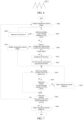
FIG. 7 is a second step flowchart of a universal serial bus interface protection method according to an embodiment of this application. As shown inFIG. 7 , the protection method in this embodiment of this application specifically includes the following steps. - S202: Enable configuration channel polling.
- S204: Determine whether a user manually disables an OTGI device, where if a determining result is yes, S206 is performed, or if the determining result is no, S208 is performed.
- S206: Keep the OTG| device off.
- Herein, S204 is performed again after S206 is performed.
- S208: Detect a configuration channel state to determine whether there is a foreign object, where if a determining result is yes, S210 is performed, or if the determining result is no, step 212 is performed.
- S210: Disable configuration channel polling, where S216 is performed again after S210 is performed.
- S212: Enable the OTG| device, where S214 is performed again after S212 is performed.
- S214: The OTG| device implements a plug-and-play function.
- S216: Determine whether a screen of the OTG| device is on, where if a determining result is yes, S218 is performed, or if the determining result is no, S220 is performed.
- S218: Determine whether the user manually enables the OTG| device, where if a determining result is yes, S220 is performed, or if the determining result is no, S222 is performed.
- S220: Determine whether the screen of the OTG| device changes from off to on, where if a determining result is yes, S202 is performed, or if the determining result is no, S224 is performed.
- S222: Keep configuration channel polling off, where S216 is performed again after S222 is performed.
- S224: Keep configuration channel polling off.
-
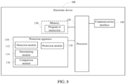
FIG. 8 is a schematic block diagram of composition of an electronic device according to an embodiment of this application. As shown inFIG. 8 , an embodiment of this application further provides anelectronic device 100, including aprocessor 120, amemory 130, and a program or an instruction that is stored in thememory 130 and executable on theprocessor 120. When the program or the instruction is executed by theprocessor 120, processes of the embodiments of the universal serial bus interface protection method can be implemented, and a same technical effect can be achieved. To avoid repetition, details are not described herein. - It should be noted that the electronic device in this embodiment of this application includes the foregoing mobile electronic device and the foregoing non-mobile electronic device.
- The
electronic device 100 includes but is not limited to aprotection apparatus 110, theprocessor 120, and thememory 130. Theprotection apparatus 110 includes adetection module 112, a determiningmodule 114, and aprotection module 118. It may be understood by a person skilled in the art that theelectronic device 100 may further include a power supply such as a battery that supplies power to each component. The power supply may be logically connected to theprocessor 120 by using a power management system, to implement functions such as charging, discharging, and power consumption management by using the power management system. A structure of the electronic device shown inFIG. 8 does not constitute a limitation on the electronic device, and may include more or fewer parts than those shown in the figure, or combine some components, or have different part arrangements. Details are not described herein again. - The
detection module 112 is configured to detect a voltage variable of a configuration channel pin. The determiningmodule 114 is configured to determine conversion time according to the voltage variable. Thecomparison module 116 is configured to compare the conversion time with preset conversion time to obtain a comparison result. In a case that the comparison result is that the conversion time is less than or equal to the preset conversion time, theprotection module 118 is configured to: when the configuration channel pin is in a short-circuit state, cut off power supply of the configuration channel pin. The determiningmodule 114 is specifically configured to determine the conversion time according to a voltage change period variable, or the determiningmodule 114 is specifically configured to determine the conversion time according to a voltage waveform variable. - The
detection module 112 is specifically configured to: cyclically detect the voltage variable of the configuration channel pin in response to a power-on instruction; or cyclically detect the voltage variable of the configuration channel pin in response to a screen-on instruction; or cyclically detect the voltage variable of the configuration channel pin in response to a configuration channel pin detection polling instruction; or cyclically detect the voltage variable of the configuration channel pin in response to in response to a universal serial bus interface connection instruction. - It should be noted that, the universal serial bus interface protection method provided in this embodiment of this application may be performed by a universal serial bus
interface protection apparatus 110, or a control module that is in the universal serial businterface protection apparatus 110 and that is configured to perform and load the universal serial bus interface protection method. In this embodiment of this application, an example in which the universal serial businterface protection apparatus 110 performs and loads the universal serial bus interface protection method is used to describe the universal serial bus interface protection method provided in the embodiments of this application. - The universal serial bus
interface protection apparatus 110 in this embodiment of this application may be an apparatus, or may be a component, an integrated circuit, or a chip in a terminal. The apparatus may be a mobile electronic device, or may be a non-mobile electronic device. For example, the mobile electronic device may be a mobile phone, a tablet computer, a notebook computer, a palmtop computer, an in-vehicle terminal device, a wearable device, an ultra-mobile personal computer (ultra-mobile personal computer, UMPC), a netbook, or a personal digital assistant (personal digital assistant, PDA), and the non-mobile electronic device may be a server, a network attached storage (Network Attached Storage, NAS), a personal computer (personal computer, PC), a television (television, TV), a counter, or a self-service machine. This is not specifically limited in this embodiment of this application. - The universal serial bus
interface protection apparatus 110 in this embodiment of this application may be an apparatus with an operating system. The operating system may be an Android (Android) operating system, may be an ios operating system, or may be another possible operating system. This is not specifically limited in this embodiment of this application. - The universal serial bus
interface protection apparatus 110 provided in this embodiment of this application can implement processes implemented by the universal serial businterface protection apparatus 110 in the method embodiment ofFIG. 1 orFIG. 7 . To avoid repetition, details are not described herein again. - An embodiment of this application further provides a readable storage medium. A program or an instruction is stored in the readable storage medium. When the program or the instruction is executed by a processor, the processes of the foregoing embodiments of the universal serial bus interface protection method can be implemented, and a same technical effect can be achieved. To avoid repetition, details are not described herein again.
- The processor is a processor in the electronic device in the foregoing embodiment. The readable storage medium includes a computer-readable storage medium such as a read-only memory (Read-Only Memory, ROM), a random access memory (Random Access Memory, RAM), a magnetic disk, an optical disc, or the like.
- An embodiment of this application further provides a chip. The chip includes a processor and a communication interface, the communication interface is coupled to the processor, and the processor is configured to run a program or an instruction to implement the processes of the foregoing embodiments of the universal serial bus interface protection method, and a same technical effect can be achieved. To avoid repetition, details are not described herein again. Examples of the shown computer readable storage medium include a non-transient computer readable storage medium such as read-only memory (Read-Only Memory, ROM for short), random access memory (Random Access Memory, RAM for short), a magnetic disk, or an optical disk.
- Aspects of this application are described with reference to a flowchart and/or a block diagram of a method, an apparatus (system), and a computer program product according to embodiments of this application. It should be understood that each block in the flowchart and/or block diagram and a combination of blocks in the flowchart and/or block diagram may be implemented by a computer program instruction. These computer program instructions may be provided to a processor of a general-purpose computer, a dedicated computer, or another programmable data processing apparatus to produce a machine, so that these instructions executed by the processor of the computer or another programmable data processing apparatus enable implementation of a function/action specified in one or more blocks of a flowchart and/or block diagram. The processor may be but is not limited to a general purpose processor, a dedicated processor, a special application processor, or a field programmable logic circuit. It may be further understood that each block in the block diagram and/or flowchart and a combination of blocks in the block diagram and/or flowchart may be implemented by dedicated hardware that performs a specified function or action, or may be implemented by a combination of dedicated hardware and a computer instruction.
- It should be understood that the chip mentioned in this embodiment of this application may also be referred to as a system-level chip, a system chip, a chip system, or a system on a chip.
- It should be noted that in this specification, the term "include", "including", or any other variant is intended to cover non-exclusive inclusion, so that a process, method, article, or apparatus that includes a series of elements includes not only those elements but also other elements that are not explicitly listed, or includes elements inherent to such a process, method, article, or apparatus. In the absence of more restrictions, an element defined by the statement "including a..." does not exclude another same element in a process, method, article, or apparatus that includes the element. In addition, it should be noted that a scope of the method and the apparatus in the embodiments of this application is not limited to: performing a function in a sequence shown or discussed, and may further include: performing a function in a basically simultaneous manner or in a reverse sequence based on an involved function. For example, the described method may be performed in a different order, and various steps may be added, omitted, or combined. In addition, features described with reference to some examples may be combined in other examples.
- According to the descriptions of the foregoing implementations, a person skilled in the art may clearly understand that the foregoing method embodiments may be implemented by using software and a required universal hardware platform, or certainly may be implemented by using hardware. However, in many cases, the former is a better implementation. Based on this understanding, this application essentially or a part contributing to a related technology may be implemented in a form of a computer software product. The computer software product is stored in a storage medium (such as a ROM/RAM, a magnetic disk, or an optical disc) and includes several instructions for instructing a terminal (which may be a mobile phone, a computer, a server, an air conditioner, or a network device) to perform the methods shown in the embodiments of this application.
- The embodiments of this application are described with reference to the accompanying drawings. However, this application is not limited to the foregoing specific implementations. The foregoing specific implementations are merely examples, but are not limiting. A person of ordinary skill in the art may make many forms without departing from the objective and the scope of the claims of this application, and these forms all fall within the protection scope of this application.
Claims (11)
- A universal serial bus interface protection method, wherein a configuration channel pin is disposed on a universal serial bus interface, and the protection method comprises:detecting a voltage variable of the configuration channel pin;determining conversion time of the voltage variable according to the voltage variable;comparing the conversion time with preset conversion time to obtain a comparison result; andcutting off power supply of the configuration channel pin in a case that the comparison result is that the conversion time is less than or equal to the preset conversion time.
- The universal serial bus interface protection method according to claim 1, wherein the determining conversion time of the voltage variable according to the voltage variable comprises:determining the conversion time according to a voltage change period variable; and/ordetermining the conversion time according to a voltage waveform variable.
- The universal serial bus interface protection method according to claim 1 or 2, wherein the detecting a voltage variable of the configuration channel pin comprises:cyclically detecting the voltage variable of the configuration channel pin in response to a power-on instruction; orcyclically detecting the voltage variable of the configuration channel pin in response to a screen-on instruction; orcyclically detecting the voltage variable of the configuration channel pin in response to a configuration channel pin detection polling instruction; orcyclically detecting the voltage variable of the configuration channel pin in response to in response to a universal serial bus interface connection instruction.
- A universal serial bus interface protection apparatus, wherein a configuration channel pin is disposed on a universal serial bus interface, and the protection apparatus comprises:a detection module (112), wherein the detection module (112) is configured to detect a voltage variable of a configuration channel pin;a determining module (114), wherein the determining module (114) is configured to determine conversion time of the voltage variable according to the voltage variable;a comparison module (116), wherein the comparison module (116) is configured to compare the conversion time with preset conversion time to obtain a comparison result; anda protection module (118), wherein in a case that the comparison result is that the conversion time is less than or equal to the preset conversion time, the protection module (118) is configured to cut off power supply of the configuration channel pin.
- The universal serial bus interface protection apparatus according to claim 4, wherein the determining module (114) is specifically configured to:determine the conversion time according to a voltage change period variable; and/ordetermine the conversion time according to a voltage waveform variable.
- The universal serial bus interface protection apparatus according to claim 4 or 5, wherein the detection module (112) is specifically configured to:cyclically detect the voltage variable of the configuration channel pin in response to a power-on instruction; orcyclically detect the voltage variable of the configuration channel pin in response to a screen-on instruction; orcyclically detect the voltage variable of the configuration channel pin in response to a configuration channel pin detection polling instruction; orcyclically detect the voltage variable of the configuration channel pin in response to in response to a universal serial bus interface connection instruction.
- An electronic device, comprising: a processor (120), a memory (130), and a program or an instruction that is stored in the memory (130) and executable on the processor (120), wherein when the program or the instruction is executed by the processor (120), steps in the universal serial bus interface protection method according to any one of claims 1 to 3 are implemented.
- An electronic device, configured to perform steps in the universal serial bus interface protection method according to any one of claims 1 to 3.
- A readable storage medium, wherein the readable storage medium stores a program or an instruction, and when the program or the instruction is executed by a processor, steps in the universal serial bus interface protection method according to any one of claims 1 to 3 are implemented.
- A chip, wherein the chip comprises a processor (120) and a communication interface (140), the communication interface (140) is coupled to the processor (120), and the processor (120) is configured to run a program or an instruction to implement steps in the universal serial bus interface protection method according to any one of claims 1 to 3.
- A computer program product, comprising a computer program that is physically comprised in a computer readable medium, and the computer program comprises program code used to perform the universal serial bus interface protection method according to any one of claims 1 to 3.
Applications Claiming Priority (2)
| Application Number | Priority Date | Filing Date | Title |
|---|---|---|---|
| CN202011477746.3A CN112558741B (en) | 2020-12-15 | 2020-12-15 | Protection method, protection device, electronic apparatus, readable storage medium, and chip |
| PCT/CN2021/136282 WO2022127659A1 (en) | 2020-12-15 | 2021-12-08 | Protection method, protection apparatus, electronic device, readable storage medium, and chip |
Publications (3)
| Publication Number | Publication Date |
|---|---|
| EP4266154A1 true EP4266154A1 (en) | 2023-10-25 |
| EP4266154A4 EP4266154A4 (en) | 2024-05-22 |
| EP4266154B1 EP4266154B1 (en) | 2025-08-13 |
Family
ID=75064714
Family Applications (1)
| Application Number | Title | Priority Date | Filing Date |
|---|---|---|---|
| EP21905588.6A Active EP4266154B1 (en) | 2020-12-15 | 2021-12-08 | Protection method, protection apparatus, electronic device, readable storage medium, and chip |
Country Status (5)
| Country | Link |
|---|---|
| US (1) | US12430273B2 (en) |
| EP (1) | EP4266154B1 (en) |
| CN (1) | CN112558741B (en) |
| ES (1) | ES3041851T3 (en) |
| WO (1) | WO2022127659A1 (en) |
Families Citing this family (3)
| Publication number | Priority date | Publication date | Assignee | Title |
|---|---|---|---|---|
| CN112558741B (en) | 2020-12-15 | 2024-07-26 | 维沃移动通信有限公司 | Protection method, protection device, electronic apparatus, readable storage medium, and chip |
| CN113672533B (en) * | 2021-08-03 | 2024-10-29 | 维沃移动通信有限公司 | Insertion detection method, device, electronic device and storage medium |
| CN119414475B (en) * | 2025-01-07 | 2025-10-03 | 江苏帝奥微电子股份有限公司 | A Type-C interface foreign body detection device and detection method |
Family Cites Families (15)
| Publication number | Priority date | Publication date | Assignee | Title |
|---|---|---|---|---|
| US7542258B2 (en) * | 2004-01-16 | 2009-06-02 | Lutron Electronics Co., Inc. | DV/dt-detecting overcurrent protection circuit for power supply |
| US9141574B2 (en) * | 2009-09-09 | 2015-09-22 | Samsung Electronics Co., Ltd. | Image forming apparatus and low power driving method thereof |
| US10148084B2 (en) * | 2014-12-24 | 2018-12-04 | Texas Instruments Incorporated | Overvoltage protection circuit for USB interface |
| CN106650512B (en) * | 2015-07-30 | 2019-09-24 | 联想(北京)有限公司 | A kind of method and electronic equipment for protecting electronic equipment |
| US10114781B2 (en) * | 2015-08-21 | 2018-10-30 | Apple Inc. | Contact corrosion mitigation |
| US10090671B2 (en) * | 2016-07-15 | 2018-10-02 | Dialog Semiconductor Inc. | Short circuit protection for data interface charging |
| US11482188B2 (en) * | 2017-05-16 | 2022-10-25 | Sony Corporation | Information processing device, control circuit, and information processing method |
| CN108664430B (en) * | 2018-05-21 | 2020-09-08 | Oppo广东移动通信有限公司 | Equipment identification method and device, storage medium and electronic equipment |
| CN108832592A (en) * | 2018-06-14 | 2018-11-16 | 珠海市魅族科技有限公司 | A kind of USB Type-C protection of connector circuit, method, apparatus and electronic equipment |
| CN109189617B (en) * | 2018-07-27 | 2021-06-29 | 维沃移动通信有限公司 | A universal serial bus type C interface detection method and terminal |
| CN111009975B (en) * | 2018-10-08 | 2022-05-31 | 立锜科技股份有限公司 | Foreign object detection method and power supply system with foreign object detection function |
| CN111026684B (en) * | 2019-12-05 | 2021-07-27 | 北京小米移动软件有限公司 | Interface control method, interface control device and storage medium |
| CN111817409B (en) * | 2020-09-11 | 2020-12-15 | 深圳英集芯科技有限公司 | Fast charging protection circuit and method, fast charging chip, and fast charging power supply device |
| CN112558741B (en) * | 2020-12-15 | 2024-07-26 | 维沃移动通信有限公司 | Protection method, protection device, electronic apparatus, readable storage medium, and chip |
| TWI812013B (en) * | 2022-02-16 | 2023-08-11 | 聯陽半導體股份有限公司 | Over voltage protection circuit for usb type-c port and related method |
-
2020
- 2020-12-15 CN CN202011477746.3A patent/CN112558741B/en active Active
-
2021
- 2021-12-08 EP EP21905588.6A patent/EP4266154B1/en active Active
- 2021-12-08 ES ES21905588T patent/ES3041851T3/en active Active
- 2021-12-08 WO PCT/CN2021/136282 patent/WO2022127659A1/en not_active Ceased
-
2023
- 2023-06-14 US US18/210,038 patent/US12430273B2/en active Active
Also Published As
| Publication number | Publication date |
|---|---|
| CN112558741B (en) | 2024-07-26 |
| US12430273B2 (en) | 2025-09-30 |
| EP4266154B1 (en) | 2025-08-13 |
| WO2022127659A1 (en) | 2022-06-23 |
| US20230325339A1 (en) | 2023-10-12 |
| EP4266154A4 (en) | 2024-05-22 |
| ES3041851T3 (en) | 2025-11-17 |
| CN112558741A (en) | 2021-03-26 |
Similar Documents
| Publication | Publication Date | Title |
|---|---|---|
| US12430273B2 (en) | Protection method, protection apparatus, electronic device, readable storage medium, and chip | |
| US12086013B2 (en) | USB interface circuit and method for low power operation | |
| US12009621B2 (en) | Device and method of ensuring power delivery in universal serial bus interface | |
| EP2698969B1 (en) | Electronic device having usb interface and usb communication start method thereof | |
| US20190393694A1 (en) | Current control and protection for universal serial bus type-c (usb-c) connector systems | |
| US20190319410A1 (en) | Overvoltage protection for universal serial bus type-c (usb-c) connector systems | |
| US20220224107A1 (en) | Circuit for and method of protecting overvoltage in universal serial bus interface | |
| US10243386B2 (en) | Power supply circuit in electronic device and control method thereof | |
| US20160091940A1 (en) | Over voltage protection for a communication line of a bus | |
| CN107316598B (en) | Hot-plug short circuit control device and method | |
| US20130024702A1 (en) | Connecting module for coupling output ends of a host device to an external storage device and method thereof | |
| US20130155565A1 (en) | Overcurrent protection circuit | |
| TWI410787B (en) | Power control circuit | |
| CN113824107B (en) | A circuit with USB OTG intelligent identification and voltage/current protection functions | |
| EP3739709B1 (en) | Over current and electrostatic discharge protection system having high operational endurance | |
| US20210184678A1 (en) | Signal Isolation System And Signal Isolation Circuit | |
| CN118889628B (en) | Charging method, circuit and electronic equipment for avoiding abnormal display | |
| CN212012118U (en) | Overvoltage protection circuit | |
| CN110704347B (en) | Protection circuits for electronic devices and related protection methods | |
| TW202123613A (en) | Overvoltage protection circuit and method thereof | |
| CN220173216U (en) | Reset circuit and electronic equipment | |
| US20250335389A1 (en) | Detection method of universal serial bus type-c | |
| TWI664785B (en) | Protection circuit applied to electronic device and associated protection method | |
| CN115765117A (en) | Power supply circuit and terminal equipment | |
| JP2024123621A (en) | Overvoltage protection circuit, connector and semiconductor device |
Legal Events
| Date | Code | Title | Description |
|---|---|---|---|
| STAA | Information on the status of an ep patent application or granted ep patent |
Free format text: STATUS: THE INTERNATIONAL PUBLICATION HAS BEEN MADE |
|
| PUAI | Public reference made under article 153(3) epc to a published international application that has entered the european phase |
Free format text: ORIGINAL CODE: 0009012 |
|
| STAA | Information on the status of an ep patent application or granted ep patent |
Free format text: STATUS: REQUEST FOR EXAMINATION WAS MADE |
|
| 17P | Request for examination filed |
Effective date: 20230710 |
|
| AK | Designated contracting states |
Kind code of ref document: A1 Designated state(s): AL AT BE BG CH CY CZ DE DK EE ES FI FR GB GR HR HU IE IS IT LI LT LU LV MC MK MT NL NO PL PT RO RS SE SI SK SM TR |
|
| DAV | Request for validation of the european patent (deleted) | ||
| DAX | Request for extension of the european patent (deleted) | ||
| REG | Reference to a national code |
Ref country code: DE Free format text: PREVIOUS MAIN CLASS: G06F0001260000 Ref country code: DE Ref legal event code: R079 Ref document number: 602021036391 Country of ref document: DE Free format text: PREVIOUS MAIN CLASS: G06F0001260000 Ipc: G06F0013380000 |
|
| A4 | Supplementary search report drawn up and despatched |
Effective date: 20240422 |
|
| RIC1 | Information provided on ipc code assigned before grant |
Ipc: G06F 13/40 20060101ALI20240416BHEP Ipc: G06F 13/38 20060101AFI20240416BHEP |
|
| GRAP | Despatch of communication of intention to grant a patent |
Free format text: ORIGINAL CODE: EPIDOSNIGR1 |
|
| STAA | Information on the status of an ep patent application or granted ep patent |
Free format text: STATUS: GRANT OF PATENT IS INTENDED |
|
| INTG | Intention to grant announced |
Effective date: 20250328 |
|
| GRAS | Grant fee paid |
Free format text: ORIGINAL CODE: EPIDOSNIGR3 |
|
| GRAA | (expected) grant |
Free format text: ORIGINAL CODE: 0009210 |
|
| STAA | Information on the status of an ep patent application or granted ep patent |
Free format text: STATUS: THE PATENT HAS BEEN GRANTED |
|
| AK | Designated contracting states |
Kind code of ref document: B1 Designated state(s): AL AT BE BG CH CY CZ DE DK EE ES FI FR GB GR HR HU IE IS IT LI LT LU LV MC MK MT NL NO PL PT RO RS SE SI SK SM TR |
|
| REG | Reference to a national code |
Ref country code: GB Ref legal event code: FG4D |
|
| REG | Reference to a national code |
Ref country code: CH Ref legal event code: EP |
|
| REG | Reference to a national code |
Ref country code: DE Ref legal event code: R096 Ref document number: 602021036391 Country of ref document: DE |
|
| REG | Reference to a national code |
Ref country code: IE Ref legal event code: FG4D |
|
| REG | Reference to a national code |
Ref country code: NL Ref legal event code: FP |
|
| REG | Reference to a national code |
Ref country code: ES Ref legal event code: FG2A Ref document number: 3041851 Country of ref document: ES Kind code of ref document: T3 Effective date: 20251117 |
|
| PGFP | Annual fee paid to national office [announced via postgrant information from national office to epo] |
Ref country code: NL Payment date: 20251126 Year of fee payment: 5 |
|
| PG25 | Lapsed in a contracting state [announced via postgrant information from national office to epo] |
Ref country code: IS Free format text: LAPSE BECAUSE OF FAILURE TO SUBMIT A TRANSLATION OF THE DESCRIPTION OR TO PAY THE FEE WITHIN THE PRESCRIBED TIME-LIMIT Effective date: 20251213 |
|
| PGFP | Annual fee paid to national office [announced via postgrant information from national office to epo] |
Ref country code: DE Payment date: 20251119 Year of fee payment: 5 |
|
| PGFP | Annual fee paid to national office [announced via postgrant information from national office to epo] |
Ref country code: GB Payment date: 20251113 Year of fee payment: 5 |
|
| PG25 | Lapsed in a contracting state [announced via postgrant information from national office to epo] |
Ref country code: NO Free format text: LAPSE BECAUSE OF FAILURE TO SUBMIT A TRANSLATION OF THE DESCRIPTION OR TO PAY THE FEE WITHIN THE PRESCRIBED TIME-LIMIT Effective date: 20251113 |
|
| REG | Reference to a national code |
Ref country code: LT Ref legal event code: MG9D |
|
| PG25 | Lapsed in a contracting state [announced via postgrant information from national office to epo] |
Ref country code: PT Free format text: LAPSE BECAUSE OF FAILURE TO SUBMIT A TRANSLATION OF THE DESCRIPTION OR TO PAY THE FEE WITHIN THE PRESCRIBED TIME-LIMIT Effective date: 20251215 |
|
| PG25 | Lapsed in a contracting state [announced via postgrant information from national office to epo] |
Ref country code: FI Free format text: LAPSE BECAUSE OF FAILURE TO SUBMIT A TRANSLATION OF THE DESCRIPTION OR TO PAY THE FEE WITHIN THE PRESCRIBED TIME-LIMIT Effective date: 20250813 |
|
| PGFP | Annual fee paid to national office [announced via postgrant information from national office to epo] |
Ref country code: IT Payment date: 20251126 Year of fee payment: 5 |
|
| PG25 | Lapsed in a contracting state [announced via postgrant information from national office to epo] |
Ref country code: HR Free format text: LAPSE BECAUSE OF FAILURE TO SUBMIT A TRANSLATION OF THE DESCRIPTION OR TO PAY THE FEE WITHIN THE PRESCRIBED TIME-LIMIT Effective date: 20250813 |
|
| PGFP | Annual fee paid to national office [announced via postgrant information from national office to epo] |
Ref country code: FR Payment date: 20251124 Year of fee payment: 5 |
|
| PG25 | Lapsed in a contracting state [announced via postgrant information from national office to epo] |
Ref country code: GR Free format text: LAPSE BECAUSE OF FAILURE TO SUBMIT A TRANSLATION OF THE DESCRIPTION OR TO PAY THE FEE WITHIN THE PRESCRIBED TIME-LIMIT Effective date: 20251114 |
|
| PG25 | Lapsed in a contracting state [announced via postgrant information from national office to epo] |
Ref country code: SE Free format text: LAPSE BECAUSE OF FAILURE TO SUBMIT A TRANSLATION OF THE DESCRIPTION OR TO PAY THE FEE WITHIN THE PRESCRIBED TIME-LIMIT Effective date: 20250813 |
|
| PG25 | Lapsed in a contracting state [announced via postgrant information from national office to epo] |
Ref country code: LV Free format text: LAPSE BECAUSE OF FAILURE TO SUBMIT A TRANSLATION OF THE DESCRIPTION OR TO PAY THE FEE WITHIN THE PRESCRIBED TIME-LIMIT Effective date: 20250813 |
|
| PG25 | Lapsed in a contracting state [announced via postgrant information from national office to epo] |
Ref country code: PL Free format text: LAPSE BECAUSE OF FAILURE TO SUBMIT A TRANSLATION OF THE DESCRIPTION OR TO PAY THE FEE WITHIN THE PRESCRIBED TIME-LIMIT Effective date: 20250813 Ref country code: BG Free format text: LAPSE BECAUSE OF FAILURE TO SUBMIT A TRANSLATION OF THE DESCRIPTION OR TO PAY THE FEE WITHIN THE PRESCRIBED TIME-LIMIT Effective date: 20250813 |
|
| PG25 | Lapsed in a contracting state [announced via postgrant information from national office to epo] |
Ref country code: RS Free format text: LAPSE BECAUSE OF FAILURE TO SUBMIT A TRANSLATION OF THE DESCRIPTION OR TO PAY THE FEE WITHIN THE PRESCRIBED TIME-LIMIT Effective date: 20251113 |
|
| REG | Reference to a national code |
Ref country code: AT Ref legal event code: MK05 Ref document number: 1825433 Country of ref document: AT Kind code of ref document: T Effective date: 20250813 |
|
| PG25 | Lapsed in a contracting state [announced via postgrant information from national office to epo] |
Ref country code: RO Free format text: LAPSE BECAUSE OF FAILURE TO SUBMIT A TRANSLATION OF THE DESCRIPTION OR TO PAY THE FEE WITHIN THE PRESCRIBED TIME-LIMIT Effective date: 20250813 |
|
| REG | Reference to a national code |
Ref country code: CH Ref legal event code: W10 Free format text: ST27 STATUS EVENT CODE: U-0-0-W10-W00 (AS PROVIDED BY THE NATIONAL OFFICE) Effective date: 20260318 |
|
| PG25 | Lapsed in a contracting state [announced via postgrant information from national office to epo] |
Ref country code: SM Free format text: LAPSE BECAUSE OF FAILURE TO SUBMIT A TRANSLATION OF THE DESCRIPTION OR TO PAY THE FEE WITHIN THE PRESCRIBED TIME-LIMIT Effective date: 20250813 |
|
| PGFP | Annual fee paid to national office [announced via postgrant information from national office to epo] |
Ref country code: ES Payment date: 20260115 Year of fee payment: 5 |
|
| PG25 | Lapsed in a contracting state [announced via postgrant information from national office to epo] |
Ref country code: DK Free format text: LAPSE BECAUSE OF FAILURE TO SUBMIT A TRANSLATION OF THE DESCRIPTION OR TO PAY THE FEE WITHIN THE PRESCRIBED TIME-LIMIT Effective date: 20250813 |
|
| PG25 | Lapsed in a contracting state [announced via postgrant information from national office to epo] |
Ref country code: AT Free format text: LAPSE BECAUSE OF FAILURE TO SUBMIT A TRANSLATION OF THE DESCRIPTION OR TO PAY THE FEE WITHIN THE PRESCRIBED TIME-LIMIT Effective date: 20250813 |
|
| RAP2 | Party data changed (patent owner data changed or rights of a patent transferred) |
Owner name: NOKIA TECHNOLOGIES OY |
|
| PG25 | Lapsed in a contracting state [announced via postgrant information from national office to epo] |
Ref country code: CZ Free format text: LAPSE BECAUSE OF FAILURE TO SUBMIT A TRANSLATION OF THE DESCRIPTION OR TO PAY THE FEE WITHIN THE PRESCRIBED TIME-LIMIT Effective date: 20250813 |
|
| PG25 | Lapsed in a contracting state [announced via postgrant information from national office to epo] |
Ref country code: SK Free format text: LAPSE BECAUSE OF FAILURE TO SUBMIT A TRANSLATION OF THE DESCRIPTION OR TO PAY THE FEE WITHIN THE PRESCRIBED TIME-LIMIT Effective date: 20250813 Ref country code: EE Free format text: LAPSE BECAUSE OF FAILURE TO SUBMIT A TRANSLATION OF THE DESCRIPTION OR TO PAY THE FEE WITHIN THE PRESCRIBED TIME-LIMIT Effective date: 20250813 |
|
| REG | Reference to a national code |
Ref country code: GB Ref legal event code: 732E Free format text: REGISTERED BETWEEN 20260409 AND 20260415 |