EP4262020A1 - Electronic device - Google Patents
Electronic device Download PDFInfo
- Publication number
- EP4262020A1 EP4262020A1 EP21913571.2A EP21913571A EP4262020A1 EP 4262020 A1 EP4262020 A1 EP 4262020A1 EP 21913571 A EP21913571 A EP 21913571A EP 4262020 A1 EP4262020 A1 EP 4262020A1
- Authority
- EP
- European Patent Office
- Prior art keywords
- radiator
- sub
- antenna element
- edge
- resonant
- Prior art date
- Legal status (The legal status is an assumption and is not a legal conclusion. Google has not performed a legal analysis and makes no representation as to the accuracy of the status listed.)
- Pending
Links
Images









Classifications
-
- H—ELECTRICITY
- H01—ELECTRIC ELEMENTS
- H01Q—ANTENNAS, i.e. RADIO AERIALS
- H01Q1/00—Details of, or arrangements associated with, antennas
- H01Q1/12—Supports; Mounting means
- H01Q1/22—Supports; Mounting means by structural association with other equipment or articles
- H01Q1/24—Supports; Mounting means by structural association with other equipment or articles with receiving set
- H01Q1/241—Supports; Mounting means by structural association with other equipment or articles with receiving set used in mobile communications, e.g. GSM
- H01Q1/242—Supports; Mounting means by structural association with other equipment or articles with receiving set used in mobile communications, e.g. GSM specially adapted for hand-held use
- H01Q1/243—Supports; Mounting means by structural association with other equipment or articles with receiving set used in mobile communications, e.g. GSM specially adapted for hand-held use with built-in antennas
-
- H—ELECTRICITY
- H01—ELECTRIC ELEMENTS
- H01Q—ANTENNAS, i.e. RADIO AERIALS
- H01Q1/00—Details of, or arrangements associated with, antennas
- H01Q1/12—Supports; Mounting means
- H01Q1/22—Supports; Mounting means by structural association with other equipment or articles
-
- H—ELECTRICITY
- H01—ELECTRIC ELEMENTS
- H01Q—ANTENNAS, i.e. RADIO AERIALS
- H01Q1/00—Details of, or arrangements associated with, antennas
- H01Q1/36—Structural form of radiating elements, e.g. cone, spiral, umbrella; Particular materials used therewith
-
- H—ELECTRICITY
- H01—ELECTRIC ELEMENTS
- H01Q—ANTENNAS, i.e. RADIO AERIALS
- H01Q1/00—Details of, or arrangements associated with, antennas
- H01Q1/52—Means for reducing coupling between antennas; Means for reducing coupling between an antenna and another structure
-
- H—ELECTRICITY
- H01—ELECTRIC ELEMENTS
- H01Q—ANTENNAS, i.e. RADIO AERIALS
- H01Q21/00—Antenna arrays or systems
- H01Q21/28—Combinations of substantially independent non-interacting antenna units or systems
-
- H—ELECTRICITY
- H01—ELECTRIC ELEMENTS
- H01Q—ANTENNAS, i.e. RADIO AERIALS
- H01Q5/00—Arrangements for simultaneous operation of antennas on two or more different wavebands, e.g. dual-band or multi-band arrangements
- H01Q5/20—Arrangements for simultaneous operation of antennas on two or more different wavebands, e.g. dual-band or multi-band arrangements characterised by the operating wavebands
-
- H—ELECTRICITY
- H01—ELECTRIC ELEMENTS
- H01Q—ANTENNAS, i.e. RADIO AERIALS
- H01Q5/00—Arrangements for simultaneous operation of antennas on two or more different wavebands, e.g. dual-band or multi-band arrangements
- H01Q5/30—Arrangements for providing operation on different wavebands
- H01Q5/307—Individual or coupled radiating elements, each element being fed in an unspecified way
-
- H—ELECTRICITY
- H01—ELECTRIC ELEMENTS
- H01Q—ANTENNAS, i.e. RADIO AERIALS
- H01Q5/00—Arrangements for simultaneous operation of antennas on two or more different wavebands, e.g. dual-band or multi-band arrangements
- H01Q5/30—Arrangements for providing operation on different wavebands
- H01Q5/307—Individual or coupled radiating elements, each element being fed in an unspecified way
- H01Q5/314—Individual or coupled radiating elements, each element being fed in an unspecified way using frequency dependent circuits or components, e.g. trap circuits or capacitors
-
- H—ELECTRICITY
- H01—ELECTRIC ELEMENTS
- H01Q—ANTENNAS, i.e. RADIO AERIALS
- H01Q5/00—Arrangements for simultaneous operation of antennas on two or more different wavebands, e.g. dual-band or multi-band arrangements
- H01Q5/40—Imbricated or interleaved structures; Combined or electromagnetically coupled arrangements, e.g. comprising two or more non-connected fed radiating elements
-
- H—ELECTRICITY
- H01—ELECTRIC ELEMENTS
- H01Q—ANTENNAS, i.e. RADIO AERIALS
- H01Q9/00—Electrically-short antennas having dimensions not more than twice the operating wavelength and consisting of conductive active radiating elements
- H01Q9/04—Resonant antennas
- H01Q9/30—Resonant antennas with feed to end of elongated active element, e.g. unipole
- H01Q9/42—Resonant antennas with feed to end of elongated active element, e.g. unipole with folded element, the folded parts being spaced apart a small fraction of the operating wavelength
-
- Y—GENERAL TAGGING OF NEW TECHNOLOGICAL DEVELOPMENTS; GENERAL TAGGING OF CROSS-SECTIONAL TECHNOLOGIES SPANNING OVER SEVERAL SECTIONS OF THE IPC; TECHNICAL SUBJECTS COVERED BY FORMER USPC CROSS-REFERENCE ART COLLECTIONS [XRACs] AND DIGESTS
- Y02—TECHNOLOGIES OR APPLICATIONS FOR MITIGATION OR ADAPTATION AGAINST CLIMATE CHANGE
- Y02D—CLIMATE CHANGE MITIGATION TECHNOLOGIES IN INFORMATION AND COMMUNICATION TECHNOLOGIES [ICT], I.E. INFORMATION AND COMMUNICATION TECHNOLOGIES AIMING AT THE REDUCTION OF THEIR OWN ENERGY USE
- Y02D30/00—Reducing energy consumption in communication networks
- Y02D30/70—Reducing energy consumption in communication networks in wireless communication networks
Definitions
- This disclosure relates to the field of communication technology, and in particular to an electronic device.
- the electronic device usually includes an antenna module for realizing the communication function of the electronic device. How to improve a communication quality of the electronic device and promote miniaturization of the electronic device has become a technical problem to be solved.
- An electronic device for improving a communication quality and facilitating miniaturization of the whole device is provided in the present disclosure.
- the electronic device includes a housing, a first antenna module, and a second antenna module.
- the housing includes a first corner portion and a second corner portion that are disposed diagonally. At least part of the first antenna module is disposed at or close to the first corner portion.
- the first antenna module includes a first radiating element. The first radiating element is configured to transmit and receive a first electromagnetic wave signal, and generate a first induction signal when a subject to-be-detected is approaching. At least part of the second antenna module is disposed at or close to the second corner portion.
- the second antenna module includes a second radiating element, and the second radiating element is configured to transmit and receive a second electromagnetic wave signal, and generate a second induction signal when the subject to-be-detected is approaching.
- the first antenna module and the second antenna module are arranged at two corners of the electronic device respectively, the first antenna module and the second antenna module can not only transmit and receive electromagnetic wave signals, but also detect approach of the subject to-be-detected in a relatively large range by using a relatively small number of antenna modules at two diagonally arranged corner portions, such that a functional integration of the antenna modules is improved, the communication quality of the electronic device is improved, and the miniaturization of the whole device of the electronic device is promoted.
- the first antenna module disposed at the first corner portion and the second antenna module disposed at the second corner portion are combined to at least detect the approach of the subject to-be-detected around the electronic device, such that the approach of the subject to-be-detected is detected omni-directionally, an intelligent detection efficiency of the electronic device for the approach of the subject to-be-detected is improved, and an operating state of the electronic device is further determined effectively, which facilitates favorable response to the operating state of the electronic device, and improves an intelligent characteristic of the electronic device.
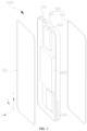
- FIG. 1 is a schematic structural diagram of an electronic device 1000 provided in implementations of the present disclosure.
- the electronic device 1000 may be a telephone, a television, a tablet computer, a mobile phone, a camera, a personal computer, a notebook computer, an on-board device, an earphone, a watch, a wearable device, a base station, an on-board radar, a customer premise equipment (CPE), and other devices capable of transmitting and receiving electromagnetic wave signals.
- the mobile phone is taken as an example of the electronic device 100.
- the electronic device 1000 is defined with reference to a first viewing angle.
- a width direction of the electronic device 1000 is defined as direction X
- a length direction of the electronic device 1000 is defined as direction Y
- a thickness direction of the electronic device 1000 is defined as direction Z.
- a direction indicated by an arrow is forward.
- the electronic device 1000 provided in implementations of the present disclosure includes a display screen 300 and a housing 500 covering the display screen 300.
- the housing 500 includes a middle frame 501 and a rear cover 502 covering the middle frame 501.
- the rear cover 502 is disposed at a side of the middle frame 501 away from the display screen 300.
- the middle frame 501 includes a middle plate and an edge frame that surrounds and is connected with a periphery of the middle plate.
- Electronic components such as a main printed circuit board 200, a battery 400, etc., are disposed on the middle plate.
- An edge of the display screen 300, the edge frame, and the rear cover 502 are connected in sequence.
- the edge frame and the rear cover 502 may be integrally formed.
- the electronic device 1000 further includes an antenna assembly 100. At least part of the antenna assembly 100 is disposed on or electrically connected with the main printed circuit board 200 of the electronic device 1000.
- the antenna assembly 100 is configured to transmit and receive a radio frequency (RF) signal to realize a communication function of the electronic device 1000.
- RF radio frequency
- the antenna assembly 100 at least includes a first antenna module 110 and a second antenna module 120.
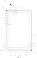
- the housing 500 includes a first corner portion 510 and a second corner portion 520 that are disposed diagonally.
- the housing 500 includes a first edge 51, a second edge 52, a third edge 53, and a fourth edge 54 that are connected in sequence.
- the first edge 51 is disposed opposite to the third edge 53.
- the second edge 52 is disposed opposite to the fourth edge 54.
- a joint between the first edge 51 and the second edge 52 is the first corner portion 510.
- a joint between the third edge 53 and the fourth edge 54 is the second corner portion 520.
- first corner portion 510 and the second corner portion 520 each are disposed on an outer surface of the edge frame.
- the first corner portion 510 may be an upper left corner of the housing 500
- the second corner portion 520 may be a lower right corner of the housing 500.
- the first corner portion 510 may be an upper right corner of the housing 500
- the second corner portion 520 may be a lower left corner of the housing 500
- the first corner portion 510 may be the lower left corner of the housing 500
- the second corner portion 520 may be the upper right corner of the housing 500
- the first corner portion 510 may be the lower right corner of the housing 500 and the second corner portion 520 may be the upper left corner of the housing 500.
- the first antenna module 110 includes a first radiating element 113.
- the first radiating element 113 is configured to transmit and receive a first electromagnetic wave signal, and generate a first induction signal when a subject to-be-detected is approaching.
- the first induction signal is used to feedback that the subject to-be-detected is approaching the first radiating element 113.
- the subject to-be-detected includes but is not limited to a human body. In implementations, the subject to-be-detected is the human body.
- the first radiating element 113 may be disposed at the first corner portion 510.
- the first radiating element 113 may be integrated on the edge frame and/or a battery cover, and disposed at or close to the first corner portion 510; or the first radiating element 113 is disposed in a space defined by the housing 500 and is disposed at or close to the first corner portion 510, for example, the first radiating element 113 is molded on a flexible circuit board and attached to the first corner portion 510 at an inner side of the first corner portion 510.
- part of the first radiating element 113 is disposed at the first edge 51 and the other part of the first radiating element 113 is disposed at the second edge 52.
- the second antenna module 120 includes a second radiating element 123.
- the second radiating element 123 is configured to transmit and receive a second electromagnetic wave signal, and generate a second induction signal when the subject to-be-detected is approaching.
- the second radiating element 123 may be disposed at the second corner portion 520.
- the second radiating element 123 may be integrated on the edge frame and/or the battery cover, and disposed at or close to the second corner portion 520; or the second radiating element 123 is disposed in the space defined by the housing 500 and is disposed at or close to the second corner portion 520, for example, the second radiating element 123 is molded on the flexible circuit board and attached to the second corner portion 520 at an inner side of the second corner portion 520.
- part of the second radiating element 123 is disposed on the third edge 53 and the other part of the second radiating element 123 is disposed on the fourth edge 54.
- the electronic device 1000 includes a front surface, a rear surface, a left side-surface, a right side-surface, an upper side-surface, and a lower side-surface.
- the front surface is disposed opposite to the rear surface.
- the front surface is a surface on which the display screen 300 is disposed and is also a surface facing a forward direction of axis Z.
- the rear surface is a surface on which the rear cover 502 is disposed and is also a surface facing a reverse direction of axis Z.
- the left side-surface is a surface facing a forward direction of axis X
- the right side-surface is a surface facing a reverse direction of axis X.
- the upper side-surface is a surface facing a forward direction of axis Y
- the lower side-surface is a surface facing a reverse direction of axis Y.
- the first radiating element 113 When the first radiating element 113 is disposed at the first corner portion 510, the first radiating element 113 is able to sense that the subject to-be-detected is approaching from the front surface, the rear surface, the left-side surface, and the upper side-surface.
- the second radiating element 123 When the second radiating element 123 is disposed at the second corner portion 520, the second radiating element 123 is able to sense that the subject to-be-detected is approaching from the front surface, the rear surface, the right-side surface, and the lower side-surface.
- the subject to-be-detected that is approaching from the front surface, the rear surface, the left side-surface, the right side-surface, the upper side-surface, and the lower side-surface can be sensed.
- the subject to-be-detected that is approaching the electronic device 1000 can be omni-directionally sensed in a spherical range, and a sensing accuracy of the electronic device 1000 for the subject to-be-detected can be improved.
- the first antenna module 110 and the second antenna module 120 are arranged at two corner portions of the electronic device 1000 respectively, the first antenna module 110 and the second antenna module 120 can not only transmit and receive electromagnetic wave signals, but also detect approach of the subject to-be-detected in a relatively large range by using the relatively small number of antenna modules 100 at two diagonally arranged corner portions, such that a functional integration of the antenna module 100 is improved, and promoting the miniaturization of the electronic device 1000 while improving a communication quality of the electronic device 1000 is improved, and miniaturization of the whole device of electronic device 1000 is promoted.
- the first antenna module 110 disposed at the first corner portion 510 and the second antenna module 120 disposed at the second corner portion 520 are combined to at least detect the approach of the subject to-be-detected form six surfaces of the electronic device 1000 (e.g., the six surfaces include the upper side-surface, the lower side-surface, the left side-surface, the right side-surface, the front surface, and the rear side-surface), such that the approach of the subject to-be-detected is detected omni-directionally, an intelligent detection efficiency of the electronic device 1000 for the approach of the subject to-be-detected is improved, an operating state of the electronic device 1000 is further determined effectively, which facilitates favorable response to the operating state of the electronic device 1000, and improves an intelligent characteristic of the electronic device 1000.
- the six surfaces include the upper side-surface, the lower side-surface, the left side-surface, the right side-surface, the front surface, and the rear side-surface
- the first antenna module 110 and the second antenna module 120 may have the same radiation band or different radiation bands.
- the first antenna module 110 and the second antenna module 120 may have different radiation bands.
- the first antenna module 110 and the second antenna module 120 may have the same radiation structure or different radiation structures.
- the first electromagnetic wave signal has a band at least covering a global positioning system L1 (GPS-L1) band, a wireless fidelity (Wi-Fi) 2.4GHz (2.4G) band, a long term evolution middle high band (LTE-MHB), a new radio middle high band (NR-MHB), a new radio ultra-high band (NR-UHB), and a Wi-Fi 5GHz (5G) band; and/or the second electromagnetic wave signal has a band at least covering a long term evolution lower band (LTE-LB), the LTE-MHB, a new radio lower band (NR-LB), the NR-MHB, and the NR-UHB.
- GPS-L1 global positioning system L1
- Wi-Fi wireless fidelity
- 2.4G long term evolution middle high band
- NR-MHB new radio middle high band
- NR-UHB new radio ultra-high band
- 5G Wi-Fi 5GHz
- the second electromagnetic wave signal has a band at least covering a long term evolution lower band (LTE-LB),
- bands of electromagnetic wave signals transmitted and received by the first antenna module 110 cover application bands of GPS, Wi-Fi, the 4th generation mobile communication technology (4G), and the 5th generation mobile communication technology (5G).
- Bands of electromagnetic wave signals transmitted and received by the second antenna module 120 cover application bands such as lower band (LB), middle high band (MHB), ultra-high band (UHB), etc., of 4G and 5G.
- the first antenna module 110 and the second antenna module 120 are jointly disposed on the electronic device 1000, such that the electronic device 1000 can cover communication bands such as LB, MHB, and UHB of common GPS, Wi-Fi, and 4G/5G.
- the first antenna module 110 is disposed at the first corner portion 510 and the second antenna module 120 is disposed at the second corner portion 520, and a structure of the first antenna module 110 and a structure of the second antenna module 120 are designed, such that the first antenna module 110 and the second antenna module 120 can cover the communication bands such as LB, MHB, and UHB of the common GPS, Wi-Fi, and 4G/5G, and the electronic device 1000 has a high functional integration, a large detection range of the subject to-be-detected, a high detection accuracy, and a large coverage of an antenna signal.
- the electronic device 1000 further includes a controller (not illustrated in the accompanying drawings) electrically connected with the first radiating element 113 and the second radiating element 123.
- the controller is configured to determine whether the subject to-be-detected is approaching the electronic device 1000 according to a magnitude of the first induction signal and a magnitude of the second induction signal.
- the first induction signal is not limited in the present disclosure, and the first induction signal may be a current signal, a voltage signal, etc.
- the controller determines that the subject to-be-detected is not approaching a periphery of the electronic device 1000.
- the preset threshold is not limited in the present disclosure, and the preset threshold may be an induction signal generated by a radiating element when a distance between the subject to-be-detected and the radiating element is 5cm.
- the controller determines that the subject to-be-detected is approaching the first edge 51 and the second edge 52 at which the first antenna module 110 of the electronic device 1000 is disposed, and no subject to-be-detected is approaching the third edge 53 and the fourth edge 54 at which the second antenna module 120 is disposed, which indicates that the electronic device 1000 is currently in an one-handed holding state at a side at which the first antenna module 110 is disposed.
- the controller When the controller detects that the first induction signal is less than the preset threshold and the second induction signal is greater than the preset threshold, the controller is configured to determine that the subject to-be-detected is approaching the third edge 53 and the fourth edge 54 at which the second antenna module 120 of the electronic device 1000 is disposed, and no subject to-be-detected is approaching the first edge 51 and the second edge 52 at which the first antenna module 110 is disposed, which indicates that the electronic device 1000 is currently in the one-handed holding state at a side of at which the second antenna module 120 is disposed.
- the controller detects that each of the first induction signal and the second induction signal is greater than the preset threshold, the controller determines that the electronic device 1000 is in a two-handed holding state at this time.
- the antenna assembly 100 disposed at an unblock position can be switched to operate, such that an influence on the communication quality is reduced when the antenna assembly 100 is in the one-handed holding state or the two-handed holding state, the antenna assembly 100 can be switched intelligently, and an intelligence of the electronic device 1000 is improved.
- the electronic device 1000 further includes a functional device (not illustrated in the accompanying drawings).
- the controller is electrically connected with functional device.
- the controller is configured to determine an operating state of the electronic device 1000 according to a magnitude of the first induction signal, a magnitude of the second induction signal, and an operating state of the functional device, and adjust power of the first antenna module 110 and power of the second antenna module 120 or control enabling and disabling of the first antenna module 110 and enabling and disabling of the second antenna module 120, according to the operating state of the electronic device 1000.
- the functional device includes a display screen 300 and a receiver (not illustrated in the accompanying drawings).
- the controller determines that the subject to-be-detected is approaching each of a position at which the first antenna module 110 is disposed and a position at which the second antenna module 120 is disposed, and the receiver is in the operating state, which indicates that the electronic device 1000 is in a state of approaching a head of the subject to-be-detected, that is, a head of a human body is close to the electronic device 1000 while making a phone call.
- the controller can control the power of the first antenna module 110 and the power of the second antenna module 120 to be reduced, to reduce a specific absorption rate of the human head for electromagnetic waves, thereby improving a safety of the electronic device 1000.
- the controller determines that the subject to-be-detected is approaching each of the position at which the first antenna module 110 is disposed and the position at which the second antenna module 120 is disposed, and the display screen 300 is in the non-display state, which indicates that the electronic device 1000 may be in a carry state.
- the carry state may be a state where the electronic device 1000 is accommodated in a clothing pocket of the subject to-be-detected, the electronic device 1000 is accommodated in a carry-on bag such as a schoolbag, a purse, and a mobile-phone bag close to the subject to-be-detected, or the electronic device 1000 is worn on a body of the subject to-be-detected through a rope, a wristband, etc., which is not limited herein.
- the controller is configured to control each of the power of the first antenna module 110 and the power of the second antenna module 120 to be reduced, such that electromagnetic radiation of the electronic device 1000 for the human body is reduced, and the specific absorption rate of the human head for the electromagnetic waves is reduced, thereby improving the safety of the electronic device 1000.
- whether the receiver is in the operating state can be further detected. If the receiver is in a non-operating state, the electronic device 1000 can be directly determined to be in a state of being accommodated in the clothing pocket of the subject to-be-detected. If the receiver is in the operating state, the electronic device 1000 can be determined to be in the state of being accommodated in the clothing pocket of the subject to-be-detected or a state of making a phone call, and the controller can control each of the power of the first antenna module 110 and the power of the second antenna module 120 to be reduced.
- the electronic device 1000 further at least includes one third antenna module 130.
- a radiation band of the at least one third antenna module 130 and a radiation band of the second antenna module 120 may be completely the same, partially overlapped, or completely non-overlapped.
- the at least one third antenna module 130 may have a structure the same as the second antenna module 120.
- the radiation band of the at least one third antenna module 130 is at least partially overlapped with the radiation band of the second antenna module 120.
- the third antenna module 130 is spaced apart from the second antenna module 120.
- the third antenna module 130 is disposed at or close to a joint between the fourth edge 54 and the first edge 51.
- the third antenna module 130 is disposed at or close to at least one of a joint between the second edge 52 and the third edge 53, the first edge 51, the second edge 52, the third edge 53, or the fourth edge 54.
- One third antenna module 130 is disposed at the joint between the fourth edge 54 and the first edge 51, and the other third antenna module 130 is disposed at the joint between the second edge 52 and the third edge 53.
- the controller is further configured to determine that the electronic device 1000 is in the holding state at an edge or a corner at which the second antenna module 120 is disposed when the second induction signal is detected to be greater than the preset threshold and the first induction signal is detected to be less than the preset threshold.
- the controller may control the power of the second antenna module 120 to increase by adjusting a frequency-tuning (FT) circuit of the second antenna module 120, such that the communication quality of the second antenna module 120 is prevented from being deteriorated due to being held, the communication quality is still good even if the second antenna module 120 is blocked, and a performance of intelligent adjustment communication of the electronic device 1000 is improved; and/or the controller may also control an unblocked third antenna module 130 to start operating, and when the third antenna module 130 starts operating, the second antenna module 120 may be turned off or continue to operate; or the controller may control the power of the third antenna module 130 that has been in the operating state to increase to ensure the communication quality of the electronic device 1000.
- FT frequency-tuning
- the electronic device 1000 further at least includes one fourth antenna module 140.
- the at least one fourth antenna module 140 has a radiation band the same as the first antenna module 110, such that when the first antenna module 110 is blocked, the at least one fourth antenna module 140 is turned on or operating power of the at least one fourth antenna module 140 is increased.
- the electronic device 1000 at least includes one third antenna module 130 and at least one fourth antenna module 140.
- the at least one third antenna module 130 has a radiation band the same as the second antenna module 120.
- the at least one fourth antenna module 140 has a radiation band the same as the first antenna module 110.
- the third antenna module 130 and the fourth antenna module 140 each are disposed at or close to at least one of the joint between the second edge 52 and the third edge 53, the joint between the fourth edge 54 and the first edge 51, the first edge 51, the second edge 52, the third edge 53, or the fourth edge 54.
- the controller is further configured to determine that the electronic device 1000 is in the holding state at both an edge or a corner at which the first antenna module 110 is disposed and an edge or a corner at which the second antenna module 120, when the first induction signal and the second induction signal each are detected to be greater than the preset threshold.
- the controller may control power of the first antenna module 110 to increase by adjusting a FT circuit of the first antenna module 110 and control the power of the second antenna module 120 to increase by adjusting the FT circuit of the second antenna module 120; and/or the controller may also control the at least one third antenna module 130 to start operating or increase power, and control the at least one fourth antenna module 140 to start operating or increase power, such that the communication quality of the first antenna module 110 and the communication quality of the second antenna module 120 are prevented from being deteriorated due to being held, the communication quality is still good even if the first antenna module 110 and the second antenna module 120 are blocked, and the performance of intelligent adjustment communication of the electronic device 1000 is improved.
- the controller can also determine a state of the electronic device 1000 through sensors such as a gyroscope sensor in the electronic device 1000, and then adjust power of each antenna module according to the state of the electronic device 1000, so as to intelligently adjust the specific absorption rate of the human body for the electromagnetic waves and improve the safety of the electronic device 1000.
- sensors such as a gyroscope sensor in the electronic device 1000
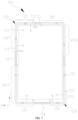
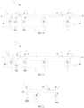
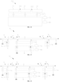
- the first antenna module 110 includes a first antenna element 10, a second antenna element 20, and a third antenna element 30 that are disposed in sequence.
- the first antenna element 10 includes a first radiator 11.
- the second antenna element 20 includes a second radiator 21.
- the third antenna element 30 includes a third radiator 31.
- the first radiating element 113 is formed by at least one of the first radiator 11, the second radiator 21, or the third radiator 31. In implementations, for example, the first radiating element 113 includes the first radiator 11, the second radiator 21, and the third radiator 31.
- a first gap 101 is defined between the first radiator 11 and the second radiator 21, and the first radiator 11 is capacitively coupled with the second radiator 21 through the first gap 101.
- a second gap 102 is defined between the second radiator 21 and the third radiator 31, and the second radiator 21 is capacitively coupled with the third radiator 31 through the second gap 102.
- the first antenna element 10 and part of the second antenna element 20 are disposed at the first edge 51, and the third antenna element 30 and the other part of the second antenna element 20 are disposed at the second edge 52.
- Part of the second radiator 21 is disposed at or close to the first edge 51 of the housing 500.
- the other part of the second radiator 21 is disposed at or close to the second edge 52 of the housing 500.
- the first radiator 11 and the third radiator 31 are disposed at different edges.
- the first radiator 11 is disposed at the first edge 51
- the third radiator 31 is disposed at the second edge 52; or the first radiator 11 is disposed at the second edge 52, and the third radiator 31 is disposed at the first edge 51.
- Part of the first radiating element 113 is disposed at or close to the first edge 51 of the housing 500.
- implementations include but are not limited to the following.
- the first radiator 11, the second radiator 21, and the third radiator 31 are integrated as part of the housing 500. Further, the first radiator 11, the second radiator 21, and the third radiator 31 are embedded in the middle frame 501 to form part of the middle frame 501.
- the middle frame 501 includes multiple metal sections 503 and insulating sections 504, and an insulating section 504 is disposed between two adjacent metal sections 503.
- the multiple metal sections 503 form the first radiator 11, the second radiator 21, and the third radiator 31 respectively.
- An insulating section 504 between the first radiator 11 and the second radiator 21 is filled in the first gap 101, and an insulating section 504 between the second radiator 21 and the third radiator 31 is filled in the second gap 102.
- the first radiator 11, the second radiator 21, and the third radiator 31 are embedded in the battery cover 502 to form part of the battery cover 502.
- the first antenna module 110 is disposed in the housing 500.
- the first radiator 11, the second radiator 21, and the third radiator 31 may be molded on the flexible circuit board and attached to an inner surface of the housing 500 or the like.
- At least one of the first radiator 11, the second radiator 21, or the third radiator 31 is configured to generate the first induction signal when the subject to-be-detected is approaching.
- the second radiator 21 may serve as a detection electrode for detecting approach of the subject to-be-detected.
- the first radiator 11 and the third radiator 31 may serve as detection electrodes for detecting the approach of the subject to-be-detected.
- the first radiator 11, the second radiator 21, and the third radiator 31 may all serve as detection electrodes for detecting the approach of the subject to-be-detected.
- the first radiator 11, the second radiator 21, and the third radiator 31 are all made of conductive materials to serve as inductive electrodes.
- charges carried by the human body change charges of the inductive electrodes, thereby generating the first induction signal.
- the first electromagnetic wave signal has a band at least covering the GPS-L1 band, the Wi-Fi 2.4G band, the LTE-MHB, the NR-MHB, the NR-UHB, and the Wi-Fi 5G band.
- the first antenna element 10 is configured to transmit and receive an electromagnetic wave signal at least covering the LTE-MHB, the NR-MHB, and the NR-UHB; and/or the second antenna element 20 is configured to transmit and receive an electromagnetic wave signal at least covering the GPS-L1 band, the Wi-Fi 2.4G band, the LTE-MHB, and the NR-MHB; and/or, the third antenna element 30 is configured to transmit and receive an electromagnetic wave signal at least covering the NR-UHB and the Wi-Fi 5G band.
- the second antenna module 120 includes a fourth antenna element 40, a fifth antenna element 50, and a sixth antenna element 60 that are disposed in sequence.
- the fourth antenna element 40 includes a fourth radiator 41.
- the fifth antenna element 50 includes a fifth radiator 51.
- the sixth antenna element 60 includes a sixth radiator 61.
- the second radiating element 123 is formed by at least one of the fourth radiator 41, the fifth radiator 51, or the sixth radiator 61. In implementations, for example, the second radiating element 123 includes the fourth radiator 41, the fifth radiator 51, and the sixth radiator 61.
- a third gap 103 is defined between the fourth radiator 41 and the fifth radiator 51, and the fourth radiator 41 is capacitively coupled with the fifth radiator 51 through the third gap 103.
- a fourth gap 104 is defined between the fifth radiator 51 and the sixth radiator 61, and the fifth radiator 51 is capacitively coupled with the sixth radiator 61 through the fourth gap 104.
- part of the fifth radiator 51 is disposed at or close to the third edge 53 of the housing 500.
- the other part of the fifth radiator 51 is disposed at or close to the fourth edge 54 of the housing 500.
- the fourth radiator 41 and the sixth radiator 61 are disposed at different edges.
- the fourth radiator 41 is disposed at the third edge 53, and the sixth radiator 61 is disposed at the fourth edge 54; or the fourth radiator 41 is disposed at the fourth edge 54 and the sixth radiator 61 is disposed at the third edge 53.
- At least one of the fourth radiator 41, the fifth radiator 51, or the sixth radiator 61 is configured to generate the second induction signal when the subject to-be-detected is approaching.
- the fifth radiator 51 may serve as a detection electrode for detecting approach of the subject to-be-detected.
- the fourth radiator 41 and the sixth radiator 61 may serve as detection electrodes for detecting the approach of the subject to-be-detected.
- the fourth radiator 41, the fifth radiator 51, and the sixth radiator 61 may all serve as detection electrodes for detecting the approach of the subject to-be-detected.
- the fourth radiator 41, the fifth radiator 51, and the sixth radiator 61 are all made of conductive materials to serve as inductive electrodes.
- charges carried by the human body change charges of the inductive electrodes, thereby generating the second induction signal.
- the second electromagnetic wave signal has a band at least covering the LTE-LB, the LTE-MHB, the NR-LB, the NR-MHB, and the NR-UHB.
- the fourth antenna element 40 is configured to transmit and receive an electromagnetic wave signal at least covering the LTE-MHB, the LTE-UHB, the NR-MHB, and the NR-UHB.
- the fifth antenna element 50 is configured to transmit and receive an electromagnetic wave signal at least covering the LTE-LB.
- the sixth antenna element 60 is configured to transmit and receive an electromagnetic wave signal at least covering the LTE-MHB, the LTE-UHB, the NR-MHB, and the NR-UHB.
- the first radiator 11 has a strip shape.
- the first radiator 11 may be molded on the housing 500 or a carrier in the housing 500 by coating, printing, or the like.
- An extension trajectory of the first radiator 11 includes, but is not limited to, a straight line, a broken line, a curve, etc.
- the extension trajectory of the first radiator 11 is the straight line.
- the shape of the first radiator 11 on the extension trajectory may be a line with a uniform width, or a line with different widths such as a line with a gradually changing width, a line with a widening region, etc.
- the first radiator 11 includes a first ground end G1, a first coupling end H1, and a first feed point A disposed between the first ground end G1 and the first coupling end H1.
- the first ground end G1 and the first coupling end H1 are two ends of the first radiator 11 respectively.
- the first ground end G1 is electrically connected with reference ground 70.
- the reference ground 70 includes a first reference ground GND1.
- the first ground end G1 is electrically connected with the first reference ground GND1.
- a first RF front-end unit 81 at least includes a first signal source 12 and a first frequency-selective filter circuit M1.
- the first frequency-selective filter circuit M1 is disposed between the first feed point A and the first signal source 12. Specifically, the first frequency-selective filter circuit M1 has an input end electrically connected with an output end of the first signal source 12, and the first frequency-selective filter circuit M1 has an output end electrically connected with the first feed point A of the first radiator 11.
- the first signal source 12 is configured to generate an excitation signal (which is also called a RF signal).
- the first frequency-selective filter circuit M1 is configured to filter out a clutter in the excitation signal transmitted by the first signal source 12, so as to form a first RF signal and transmit the first RF signal to the first radiator 11, such that the first radiator 11 transmits and receives a first electromagnetic wave sub-signal.
- the second radiator 21 has a strip shape.
- the second radiator 21 may be molded on the housing 500 or on a carrier in the housing 500 by coating, printing, or the like.
- An extension trajectory of the second radiator 21 includes, but is not limited to, a straight line, a broken line, a curve, etc.
- the extension trajectory of the second radiator 21 is the straight line.
- the shape of the second radiator 21 on the extension trajectory may be a line with a uniform width, or a line with different widths such as a line with a gradually changing width, a line with a widening region, etc.
- the second radiator 21 includes a second coupling end H2, a third coupling end H3 disposed opposite to the second coupling end H2, and a second feed point C disposed between the second coupling end H2 and the third coupling end H3.
- the second coupling end H2 is spaced apart from the first coupling end H1 to define the first gap 101.
- the first gap 101 is defined between the second radiator 21 and the first radiator 11.
- the first radiator 11 is capacitively coupled with the second radiator 21 through the first gap 101.
- Capacitive coupling means that an electric field is generated between the first radiator 11 and the second radiator 21, a signal of the first radiator 11 can be transmitted to the second radiator 21 through the electric field, and a signal of the second radiator 21 can be transmitted to the first radiator 11 through the electric field, such that electrical signal conduction between the first radiator 11 and the second radiator 21 can still be realized even if the first radiator 11 is disconnected from the second radiator 21.
- a second RF front-end unit 82 includes a second signal source 22 and a second frequency-selective filter circuit M2.
- the reference ground 70 further includes a second reference ground GND2.
- the second reference ground GND2 and the first reference ground GND1 may be the same reference ground or different reference grounds.
- the second frequency-selective filter circuit M2 is disposed between the second feed point C and the second signal source 22. Specifically, the second frequency-selective filter circuit M2 has an input end electrically connected with the second signal source 22, and the output end electrically connected with the second radiator 21.
- the second signal source 22 is configured to generate an excitation signal.
- the second frequency-selective filter circuit M2 is configured to filter out a clutter in the excitation signal transmitted by the second signal source 22, so as to form a second RF signal and transmit the second RF signal to the second radiator 21, such that the second radiator 21 transmits and receives a second electromagnetic wave sub-signal.
- the third radiator 31 has a strip shape.
- the third radiator 31 may be molded on the housing 500 or on a carrier in the housing 500 by coating, printing, or the like.
- An extension trajectory of the third radiator 31 includes, but is not limited to, a straight line, a broken line, a curve, etc.
- the extension trajectory of the third radiator 31 is the straight line.
- the shape of the third radiator 31 on the extension trajectory may be a line with a uniform width, or a line with different widths such as a line with a gradually changing width, a line with widening region, etc.
- the third radiator 31 includes a fourth coupling end H4, a second ground end G2, and a third feed point E disposed between the fourth coupling end H4 and the second ground end G2.
- the fourth coupling end H4 and the second ground end G2 are two ends of the third radiator 31.
- the second gap 102 is defined between the fourth coupling end H4 and the third coupling end H3.
- a third RF front-end unit 83 includes a third signal source 32 and a third frequency-selective filter circuit M3.
- the third frequency-selective filter circuit M3 has one end electrically connected with the third feed point E, and the other end electrically connected with the third signal source 32.
- the third frequency-selective filter circuit M3 is configured to filter out a clutter in a RF signal transmitted by the third signal source 32 to form a third RF signal, and transmit the third RF signal to the third radiator 31 to excite the third radiator 31 to transmit and receive a third electromagnetic wave signal.
- the reference ground 70 further includes a third reference ground GND3.
- the third frequency-selective filter circuit M3 and the second ground end G2 each are electrically connected with the third reference ground GND3.
- the third reference ground GND3, the second reference ground GND2, and the first reference ground GND1 may have an integral structure or separate structures.
- each of the first radiator 11, the second radiator 21, and the third radiator 31 includes, but is not limited to, at least one of a flexible printed circuit (FPC) antenna radiator, a laser direct structuring (LDS) antenna radiator, a print direct structuring (PDS) antenna radiator, or a metal branch.
- FPC flexible printed circuit
- LDS laser direct structuring
- PDS print direct structuring
- a material of each of the first radiator 11, the second radiator 21, and the third radiator 31 is a conductive material, and the specific material includes, but is not limited to, a metal, a transparent conductive oxide (e.g., indium tin oxide (ITO)), a carbon nanotube, graphene, etc.
- the material of each of the first radiator 11, the second radiator 21, and the third radiator 31 is a metal material, such as silver, copper, etc.
- the first signal source 12, the second signal source 22, the third signal source 32, the first frequency-selective filter circuit M1, the second frequency-selective filter circuit M2, and the third frequency-selective filter circuit M3 are all disposed on the main board 200 of the electronic device 1000.
- the first signal source 12, the second signal source 22, and the third signal source 32 are the same signal source, or the first signal source 12, the second signal source 22, and the third signal source 32 are different sources.
- the first signal source 12, the second signal source 22, and the third signal source 32 are the same signal source.
- the same signal source is configured to transmit excitation signals towards the first frequency-selective filter circuit M1, the second frequency-selective filter circuit M2, and the third frequency-selective filter circuit M3 respectively.
- the first frequency-selective filter circuit M1, the second frequency-selective filter circuit M2, and the third frequency-selective filter circuit M3 have different circuit structures
- the first frequency-selective filter circuit M1, the second frequency-selective filter circuit M2, and the third frequency-selective filter circuit M3 have different gated bands, such that the first radiator 11, the second radiator 21, and the third radiator 31 respectively transmit and receive a first electromagnetic wave, a second electromagnetic wave, and a third electromagnetic wave under different excitation signals.
- a band of the first electromagnetic wave sub-signal, a band of the second electromagnetic wave sub-signal, and a band of the third electromagnetic wave signal are different from one another, such that the first antenna module 110 covers a relatively wide band, a signal transceiving isolation between various antenna elements is relatively high, and interference is little.
- the first signal source 12, the second signal source 22, and the third signal source 32 are different from one another.
- the first signal source 12, the second signal source 22, and the third signal source 32 may be integrated on the same chip or separately packaged on different chips.
- the first signal source 12 is configured to generate a first excitation signal.
- the first excitation signal is filtered by the first frequency-selective filter circuit M1 to form the first RF signal.
- the first RF signal is loaded on the first radiator 11, such that the first radiator 11 transmits and receives the first electromagnetic wave sub-signal.
- the second signal source 22 is configured to generate a second excitation signal.
- the second excitation signal is filtered by the second frequency-selective filter circuit M2 to form the second RF signal.
- the second RF signal is loaded on the second radiator 21, such that the second radiator 21 transmits and receives the second electromagnetic wave sub-signal.
- the third signal source 32 is configured to generate the third excitation signal.
- the third excitation signal is filtered by the third frequency-selective filter circuit M3 to form the third RF signal.
- the third RF signal is loaded on the third radiator 31, such that the third radiator 31 transmits and receives the third electromagnetic wave signal.
- the first antenna element 10, the second antenna element 20, and the third antenna element 30 can transmit and receive electromagnetic wave signals of different bands, thereby improving isolation between the first antenna element 10, the second antenna element 20, and the third antenna element 30.
- the first frequency-selective filter circuit M1, the second frequency-selective filter circuit M2, and the third frequency-selective filter circuit M3 can also make the electromagnetic wave signals transmitted and received by the first antenna element 10, the second antenna element 20, and the third antenna element 30 have little or no interference with one another.
- the first frequency-selective filter circuit M1 includes, but is not limited to, capacitors, inductors, resistors, etc. connected in series and/or in parallel.
- the first frequency-selective filter circuit M1 may include multiple branches formed by the capacitors, the inductors, and the resistors connected in series and/or in parallel, and switches for controlling on/off of the multiple branches.
- frequency-selective parameters including a resistance value, an inductance value, and a capacitance value
- a filtering range of the first frequency-selective filter circuit M1 can be adjusted, such that the first frequency-selective filter circuit M1 can obtain the first RF signal from the excitation signal transmitted by the first signal source 12, and then the first antenna element 10 can transmit and receive the first electromagnetic wave sub-signal.
- the second frequency-selective filter circuit M2 and the third frequency-selective filter circuit M3 each include multiple branches formed by capacitors, inductors, and resistors connected in series and/or in parallel, and switches for controlling the on/off of the multiple branches.
- the first frequency-selective filter circuit M1, the second frequency-selective filter circuit M2, and the third frequency-selective filter circuit M3 have different structures.
- the first frequency-selective filter circuit M1 is configured to adjust an impedance of a radiator electrically connected with the first frequency-selective filter circuit M1, such that the impedance of the radiator electrically connected with the first frequency-selective filter circuit M1 matches a frequency at which the radiator generates resonance, thereby realizing relatively large transceiving power of the radiator.
- the second frequency-selective filter circuit M2 is configured to adjust an impedance of a radiator electrically connected with the second frequency-selective filter circuit M2, such that the impedance of the radiator electrically connected with the second frequency-selective filter circuit M2 matches a frequency at which the radiator generates resonance, thereby realizing relatively large transceiving power of the radiator.
- the third frequency-selective filter circuit M3 is configured to adjust an impedance of a radiator electrically connected with the third frequency-selective filter circuit M3, such that the impedance of the radiator electrically connected with the third frequency-selective filter circuit M3 matches a frequency at which the radiator generates resonance, thereby realizing relatively large transceiving power of the radiator. Therefore, the first frequency-selective filter circuit M1, the second frequency-selective filter circuit M2, the third frequency-selective filter circuit M3 each can also be called a matching circuit.
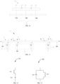
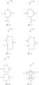
- FIG. 12 to FIG. 19 are schematic diagrams of first frequency-selective filter circuits M1 provided by various implementations.
- the first frequency-selective filter circuit M1 includes one or more of following circuits.
- the first frequency-selective filter circuit M1 includes a band-pass circuit formed by an inductor L0 and a capacitor C0 connected in series.
- the first frequency-selective filter circuit M1 includes a bandstop circuit formed by an inductor L0 and a capacitor C0 connected in parallel.
- the first frequency-selective filter circuit M1 includes an inductor L0, a first capacitor C1, and a second capacitor C2.
- the inductor L0 is connected with the first capacitor C1 in parallel, and the second capacitor C2 is electrically connected with a node where the inductor L0 is electrically connected with the first capacitor C1.
- the first frequency-selective filter circuit M1 includes a capacitor C0, a first inductor L1, and a second inductor L2.
- the capacitor C0 is connected with the first inductor L1 in parallel, and the second inductor L2 is electrically connected with a node where the capacitor C0 is electrically connected with the first inductor L1.
- the first frequency-selective filter circuit M1 includes an inductor L0, a first capacitor C1, and a second capacitor C2.
- the inductor L0 is connected with the first capacitor C1 in series.
- One end of the second capacitor C2 is electrically connected with a first end of the inductor L0 that is not connected with the first capacitor C1, and another end of the second capacitor C2 is electrically connected with one end of the first capacitor C1 which is not connected with the inductor L0.
- the first frequency-selective filter circuit M1 includes a capacitor C0, a first inductor L1, and a second inductor L2.
- the capacitor C0 is connected with the first inductor L1 in series.
- One end of the second inductor L2 is electrically connected with one end of the capacitor C0 which is not connected with the first inductor L1, and another end of the second inductor L2 is electrically connected with one end of the first inductor L1 which is not connected with the capacitor C0.
- the first frequency-selective filter circuit M1 includes a first capacitor C1, a second capacitor C2, a first inductor L1, and a second inductor L2.
- the first capacitor C1 is connected with the first inductor L1 in parallel
- the second capacitor C2 is connected with the second inductor L2 in parallel.
- One end of the circuit formed by the second capacitor C2 and the second inductor L2 connected in parallel is electrically connected with one end of the circuit formed by the first capacitor C1 and the first inductor L1 connected in parallel.
- the first frequency-selective filter circuit M1 includes a first capacitor C1, a second capacitor C2, a first inductor L1, and a second inductor L2.
- the first capacitor C1 is connected with the first inductor L1 in series to define a first unit 111
- the second capacitor C2 is connected with the second inductor L2 in series to define a second unit 112
- the first unit 111 is connected with the second unit 112 in parallel.
- the second frequency-selective filter circuit M2 may include one or more of circuits of FIG. 12 to FIG. 19 .
- the third frequency-selective filter circuit M3 may include one or more of circuits in FIG. 12 to FIG. 19 .
- the first frequency-selective filter circuit M1 presents different band-pass and bandstop characteristics in different bands.
- a resonant frequency of the first antenna element 10 a resonant frequency of the second antenna element 20, and a resonant frequency of the third antenna element 30 can be shifted towards a low frequency or a high frequency, such that a relatively wide bandwidth of the first antenna module 110 is realized to cover the GPS band, the Wi-Fi band, the 4G band, the 5G band, and even more bands at the same time, and coverage and communication quality of an antenna signal of the first antenna module 100 are improved.
- a manner of FT provided in the present disclosure will be described below with reference to the accompanying drawings to obtain suitable impedance matching and increase the power of the first antenna module 110.
- a manner of FT of an antenna element provided in the present disclosure includes, but is not limited to, aperture FT and matching FT.
- a resonant frequency of an antenna element is shifted towards the low frequency or the high frequency, such that the antenna element can transmit and receive an electromagnetic wave of a required band.
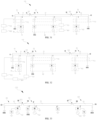
- the second radiator 21 further includes a first coupling point B disposed at a side of the second coupling end H2 away from the first coupling end H1.
- the second antenna element 20 further includes a first FT circuit T1.
- the first FT circuit T1 has one end electrically connected with the first coupling point B and the other end grounded.
- the first FT circuit T1 is directly electrically connected with the second radiator 21 to adjust an impedance matching characteristic of the second radiator 21, thereby realizing the aperture FT.
- the first FT circuit T1 may also be electrically connected with the second frequency-selective filter circuit M2, and the first FT circuit T1 and the second frequency-selective filter circuit M2 form a new matching circuit to adjust the impedance matching characteristic of the second radiator 21, thereby realizing matching FT.
- the first FT circuit T1 includes a combination of a switch and at least one of a capacitor or an inductor; and/or the first FT circuit T1 includes a variable capacitor.
- the first FT circuit T1 includes, but is not limited to, capacitors, inductors, resistors, etc., connected in series and/or in parallel.
- the first FT circuit T1 may include multiple branches formed by the capacitors, the inductors, and the resistors connected in series and/or in parallel, and switches for controlling on/off of the multiple branches. By controlling on/off of different switches, frequency-selective parameters (including a resistance value, an inductance value, and a capacitance value) of the first FT circuit T1 can be adjusted, such that an impedance of the second radiator 21 can be adjusted, and then a resonant frequency-point of the second radiator 21 can be adjusted.
- a specific structure of the first FT circuit T1 is not limited in the present disclosure.
- the first FT circuit T1 may include one or more of circuits in FIG. 12 to FIG. 19 .
- the first FT circuit T1 includes, but is not limited to, a variable capacitor. By adjusting a capacitance value of the variable capacitor, the FT parameters of the first FT circuit T1 are adjusted, such that the impedance of the second radiator 21 is adjusted, and then the resonant frequency-point of the second radiator 21 is adjusted.
- the FT parameters e.g., a resistance value, a capacitance value, and an inductance value
- the FT parameters e.g., a resistance value, a capacitance value, and an inductance value
- the impedance of the second radiator 21 is adjusted to adjust the impedance of the second radiator 21, such that the resonant frequency-point of the second radiator 21 is shifted towards a high band (HB) or a LB in a small range.
- HB high band
- LB LB
- the first antenna element 10 further includes a second FT circuit T2.
- the first radiator 11 further includes a first FT point F.
- the first FT point F is disposed between the first feed point A and the first coupling end H1.
- the second FT circuit T2 has one end electrically connected with the first FT point F or the first frequency-selective filter circuit M1, and the other end grounded.
- the second FT circuit T2 is directly electrically connected with the first radiator 11 to adjust an impedance matching characteristic of the first radiator 11, thereby realizing the aperture FT.
- the second FT circuit T2 may also be electrically connected with the first frequency-selective filter circuit M1, and the second FT circuit T2 and the first frequency-selective filter circuit M1 form a new matching circuit to adjust the impedance matching characteristic of the first radiator 11, thereby realizing the matching FT.
- the second FT circuit T2 includes a combination of a switch and at least one of a capacitor and an inductor; and/or the second FT circuit T2 includes a variable capacitor.
- the second FT circuit T2 includes, but is not limited to, capacitors, inductors, resistors, etc., disposed in series and/or in parallel.
- the second FT circuit T2 may include multiple branches formed by the capacitors, the inductors, and the resistors connected in series and/or in parallel, and switches for controlling on/off of the multiple branches. By controlling the on/off of different switches, frequency-selective parameters (including a resistance value, an inductance value, and a capacitance value) of the second FT circuit T2 can be adjusted, such that an impedance of the first radiator 11 can be adjusted, and then a resonant frequency-point of the first radiator 11 can be adjusted.
- a specific structure of the second FT circuit T2 is not limited in the present disclosure.
- the second FT circuit T2 may include one or more of the circuits in FIG. 12 to FIG. 19 .
- the second FT circuit T2 includes, but is not limited to, a variable capacitor. By adjusting a capacitance value of the variable capacitor, FT parameters of the second FT circuit T2 are adjusted, such that the impedance of the first radiator 11 is adjusted, and then the resonant frequency of the first radiator 11 is adjusted.
- the FT parameters e.g., a resistance value, a capacitance value, and an inductance value
- the FT parameters e.g., a resistance value, a capacitance value, and an inductance value
- the FT parameters are adjusted to adjust the impedance of the first radiator 11, such that the resonant frequency-point of the first radiator 11 is shifted towards a HB or a LB in a small range.
- a frequency coverage range of the first antenna element 10 in a relatively wide band can be improved.
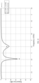
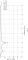
- FIG. 22 is an equivalent circuit diagram of the first antenna element 10. Part of the second antenna element 20 is capacitively coupled with the first antenna element 10. Referring to FIG. 23, FIG. 23 is a return loss graph of the first antenna element 10.
- the number and structure of antenna elements of the first antenna module 110 are designed, and an effective electrical length and a structure of the first radiator 11 of the first antenna element 10, a position of the first feed point A, an effective electrical length of the second radiator 21 coupled with the first radiator 11, etc., are also designed, such that a resonant mode is formed in a band with relatively high practicability to transmit and receive an electromagnetic wave in the band with the relatively high practicability.
- the impedance matching of the first radiator 11 is adjusted by FT circuits (including the first FT circuit T1 and the second FT circuit T2), such that the resonant mode of the first antenna element 10 is shifted towards a HB and a LB.
- the effective electrical length refers to a length at which the first RF signal acts on the first radiator 11.
- the effective electrical length may be an actual length of the first radiator 11, or may be slightly shorter or longer than the actual length of the first radiator 11.
- the first radiator 11 of the first antenna element 10 by designing the effective electrical length of the first radiator 11, the first radiator 11 from the first ground end G1 to the first coupling end H1 is configured to generate an electromagnetic wave signal in a first resonant mode a under excitation of a RF signal transmitted by the first signal source 12.
- the first radiator 11 from the first feed point A to the second coupling end H2 is configured to generate a second resonant mode b under excitation of a RF signal transmitted by the first signal source 12.
- a band of the first resonant mode a and a band of the second resonant mode b jointly cover 2GHz ⁇ 4GHz.
- the first resonant mode a is a 1/4-wavelength fundamental mode in which the first antenna element 10 from the first ground end G1 to the first coupling end H1 is operable. It can be understood that the 1/4-wavelength fundamental mode is a relatively efficient resonant mode of the first RF signal from the first ground end G1 to the first coupling end H1.
- the first antenna element 10 When the first antenna element 10 is operable in the fundamental mode, the first antenna element 10 has relatively high transceiving power.
- a band covered by the first resonant mode a has relatively high transceiving power.
- the band covered by the first resonant mode a includes, but is not limited to, B40 ⁇ 41 and N41.
- an effective electrical length of the first radiator 11 from the first ground end G1 to the first coupling end H1 is designed, for example, the length from the first ground end G1 to the first coupling end H1 is about 2.9cm, and a parameter of the first FT circuit T1 and a parameter of the first frequency-selective filter circuit M1 are adjusted, such that the first radiator 11 from the first ground end G1 to the first coupling end H1 radiates in the first resonant mode a of the 1/4-wavelength fundamental mode.
- the first resonant mode a has a resonant frequency of about 2.5495 gigahertz (GHz).
- the second resonant mode b is a 1/4-wavelength fundamental mode in which the first antenna element 10 from the first feed point A to the first coupling end H1 is operable.
- the first antenna element 10 has relatively high transceiving power.
- a band covered by the second resonant mode b has higher transceiving power.
- the band covered by the second resonant mode b includes, but is not limited to, N77 and N78.
- an effective electrical length of the first radiator 11 from the first feed point A to the first coupling end H1 is designed, for example, the length from the first feed point A to the first coupling end H1 is about 2.1cm, and the parameter of the first FT circuit T1 and the parameter of the first frequency-selective filter circuit M1 are adjusted, such that the first radiator 11 from the first feed point A to the first coupling end H1 radiates in the second resonant mode b of the 1/4-wavelength fundamental mode.
- the second resonant mode b has a resonant frequency of about 3.5293GHz.
- the size and structure of the first radiator 11 and the position of the first feed point A are designed, and the parameter of the first FT circuit T1 is adjusted, such that the first radiator 11 can cover a certain band in a band of 2GHz ⁇ 4GHz, thereby covering B40 ⁇ 41, N41, N77, and N78 and having relatively high transceiving power in B40 ⁇ 41, N41, N77, and N78.
- the second radiator 21 from the first coupling point B to the second coupling end H2 is configured to be capacitively coupled with the first radiator 11. Specifically, a length of the second radiator 21 from the first coupling point B to the second coupling end H2 is less than 1/4 of a wavelength of an electromagnetic wave at a resonant frequency-point of the second resonant mode b. The length of the second radiator 21 from the first coupling point B to the second coupling end H2 is less than 2.1cm.
- the second antenna element 20 plays a role of capacitive loading for the first antenna element 10, such that the electromagnetic wave signal radiated by the first antenna element 10 is shifted to the LB, and a radiation efficiency of the first antenna element 10 can be improved.
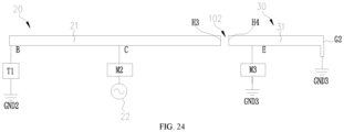
- FIG. 24 is an equivalent circuit diagram of the second antenna element 20.
- the third antenna element 30 is capacitively coupled with the second antenna element 20.
- FIG. 25 is a return loss graph of the second antenna element 20.
- the number and structure of antenna elements of the first antenna module 110 are designed, and an effective electrical length and a structure of the second radiator 21 of the second antenna element 20, a position of the second feed point C, an effective electrical length of the third radiator 31 coupled with the second radiator 21, etc., are also designed, such that a resonant mode is formed in a band with a relatively high practicability to transmit and receive an electromagnetic wave in the band with the relatively high practicability.
- the impedance matching of the second radiator 21 is adjusted by FT circuits (including the second FT circuit T2, the second frequency-selective filter circuit M2, the third frequency-selective filter circuit M3), such that the resonant mode of the second antenna element 20 is shifted towards a HB and a LB.
- the second antenna element 20 has a relatively wide bandwidth in the band with the relatively high practicability.
- the effective electrical length refers to a length at which the second RF signal acts on the second radiator 21.
- the effective electrical length may be an actual length of the second radiator 21, or may be slightly shorter or longer than the actual length of the second radiator 21.
- the second radiator 21 from the first coupling point B to the third coupling end H3 is configured to generate a third resonant mode c under excitation of a RF signal transmitted by the second signal source.
- the second radiator 21 from the second feed point C to the third coupling end H3 is configured to generate a fourth resonant mode d under excitation of a RF signal transmitted by the second signal source 22.
- a band of the third resonant mode c and a band of the fourth resonant mode d jointly cover 1.5GHz ⁇ 3GHz.
- the third resonant mode c is a 1/4-wavelength fundamental mode in which the second antenna element 20 from the first coupling point B to the third coupling end H3 is operable.
- the second antenna element 20 When operating in the fundamental mode, the second antenna element 20 has relatively high transceiving power.
- a band covered by the third resonant mode c has relatively high transceiving power.
- the band covered by the third resonant mode c includes, but is not limited to, GPS-L1, B3, and N3.
- an effective electrical length of the second radiator 21 from the first coupling point B to the third coupling end H3 is designed, for example, the length between the first coupling point B and the third coupling end H3 is about 4.6cm, and a parameter of the second FT circuit T2, a parameter of the second frequency-selective filter circuit M2, and a parameter of the third frequency-selective filter circuit M3 are adjusted, such that the second radiator 21 from the first coupling point B to the third coupling end H3 radiates in the third resonant mode c of the 1/4-wavelength fundamental mode.
- the third resonant mode c has a resonant frequency of about 1.618GHz.
- the fourth resonant mode d is a 1/4-wavelength fundamental mode in which the second antenna element 20 from the second feed point C to the third coupling end H3 is operable.
- the second antenna element 20 has relatively high transceiving power.
- the band covered by the fourth resonant mode d has the relatively high transceiving power.
- the band covered by the fourth resonant mode d includes, but is not limited to, Wi-Fi 2.4GHz band, B7 ⁇ 40 ⁇ 41, N7, and N41.
- an effective electrical length of the second radiator 21 from the second feed point C to the third coupling end H3 is designed, for example, the length from the second feed point C to the third coupling end H3 is about 2.1cm, and the parameter of the first FT circuit T1, the parameter of the second frequency-selective filter circuit M2, and the parameter of the third frequency-selective filter circuit M3 are adjusted, such that the second radiator 21 from the second feed point C to the third coupling end H3 radiates in the fourth resonant mode d of the 1/4-wavelength fundamental mode.
- the fourth resonant mode d has a resonant frequency of about 2.4943GHz.
- the size and structure of the second radiator 21 and the position of the second feed point C are designed, and the parameter of the first FT circuit T1, the parameter of the second frequency-selective filter circuit M2, and the parameter of the third frequency-selective filter circuit M3 are adjusted, such that the second radiator 21 can cover a certain band in a range of 1.5GHz ⁇ 3GHz, thereby covering GPS-L1 band, Wi-Fi 2.4 band, B3 ⁇ 7 ⁇ 40 ⁇ 41, and N3 ⁇ 7 ⁇ 41 and having relatively high transceiving power in Wi-Fi 2.4 band, B3 ⁇ 7 ⁇ 40 ⁇ 41, and N3 ⁇ 7 ⁇ 41.
- first resonant mode a, the second resonant mode b , the third resonant mode c, and the fourth resonant mode b may be generated simultaneously, or one or more of the first resonant mode a, the second resonant mode b , the third resonant mode c, and the fourth resonant mode b may be generated.
- FIG. 16 is an equivalent circuit diagram of the third antenna element 30.
- the second antenna element 20 is capacitively coupled with the third antenna element 30.
- FIG 27 is a return loss graph of the third antenna element 30.
- an effective electrical length and a structure of the third radiator 31 in the radiator element 30, a position of the third feed point, an effective electrical length of coupling between the second radiator 21 and the third radiator 31 are designed, such that a resonant mode is formed in a band with relatively high practicability to transmit and receive an electromagnetic wave in the band with the relatively high practicability.
- the impedance matching of the third radiator 31 is adjusted by FT circuits (including the second FT circuit T2, the second frequency-selective filter circuit M2, and the third frequency-selective filter circuit M3), such that the resonant mode of the third radiator element 30 is shifted towards a HB and a LB.
- the effective electrical length refers to a length at which the third RF signal acts on the third radiator 31.
- the effective electrical length may be an actual length of the third radiator 31, or may be slightly shorter or longer than the actual length of the third radiator 31.
- the third radiator 31 of the third antenna element 30 by designing the effective electrical length of the third radiator 31, the third radiator 31 from the second ground end G2 to the fourth coupling end H4 is configured to generate a fifth resonant mode e and a sixth resonant mode f under excitation of a RF signal transmitted by the third signal source 32.
- the second radiator 21 from the first coupling point B to the third coupling end H3 is configured to generate a seventh resonant mode g under excitation of a RF signal transmitted by the third signal source 32.
- a band of the fifth resonant mode e, a band of the sixth resonant mode f , and a band of the seventh resonant mode g jointly cover 3GHz ⁇ 6.5GHz.
- the fifth resonant mode e is a 1/8-wavelength mode in which the third antenna element 30 from the second ground end G2 to the fourth coupling end H4 is operable.
- the fifth resonant mode e is a 1/4 ⁇ 1/8-wavelength mode in which the third antenna element 30 from the second ground end G2 to the fourth coupling end H4 is operable.
- a band covered by the fifth resonant mode e includes, but is not limited to, N77/78.
- an effective electrical length of the third radiator 31 from the second ground end G2 to the fourth coupling end H4 is designed, for example, the length from the second ground end G2 to the fourth coupling end H4 is about 1.1cm ⁇ 2.2cm, and a parameter of the second FT circuit T2, a parameter of the second frequency-selective filter circuit M2, and a parameter of the third frequency-selective filter circuit M3 are adjusted, such that the third radiator 31 from the second ground end G2 to the fourth coupling end H4 radiates in the fifth resonant mode e of the 1/8-wavelength fundamental mode.
- the fifth resonant mode e has a resonant frequency of about 3.4258GHz.
- the third feed point E is close to the fourth coupling end H4.
- the third feed point E is close to the second gap 102, such that the third feed point is a capacitive coupled feed point, and the third radiator 31 from the second ground end G2 to the fourth coupling end H4 is more easily excited to generate the 1/8-wavelength fundamental mode, so as to better cover N77/78 and have relatively high operating power in N77/78.
- the sixth resonant mode f is a 1/4-wavelength fundamental mode in which the third antenna element 30 from the second ground end G2 to the fourth coupling end H4 is operable.
- the third antenna element 30 has relatively high transceiving power.
- a band covered by the sixth resonant mode f has the relatively high transceiving power.
- the band covered by the sixth resonant mode f includes, but is not limited to, the Wi-Fi 5GHz band.
- an effective electrical length of the second radiator 21 from the second feed point C to the third coupling end H3 is designed, for example, the length from the second feed point C to the third coupling end H3 is about 1.3cm, and the parameter of the first FT circuit T1, the parameter of the second frequency-selective filter circuit M2, and the parameter of the third frequency-selective filter circuit M3 are adjusted, such that the second radiator 21 from the second feed point C to the third coupling end H3 radiates in the sixth resonant mode f of the 1/4-wavelength fundamental mode.
- the sixth resonant mode f has a resonant frequency of about 5.7357GHz.
- the seventh resonant mode g is a 1/2 wavelength mode in which the third antenna element 30 from the first coupling point B to the third coupling end H3 is operable.
- the fifth resonant mode e, the sixth resonant mode f , and the seventh resonant mode g may be generated simultaneously, or one or more of the fifth resonant mode e, the sixth resonant mode f , and the seventh resonant mode g may be generated may be generated.
- the first electromagnetic wave sub-signal transmitted and received by the first antenna element 10 at least covers B40/41+N41/78/77.
- B40 covers 2.3GHz ⁇ 2.5GHz
- B41 covers 2.5GHz ⁇ 2.69GHz
- N41 covers 2.49GHz ⁇ 2.69GHz
- N78 covers 3.3GHz ⁇ 3.8GHz
- N77 covers 3.3GHz ⁇ 4.2GHz.
- the second electromagnetic wave sub-signal transmitted and received by the second antenna element 20 covers at least (GPS-L1 band)+(Wi-Fi 2.4G band)+(LTE-MHB)+(NR-MHB), the GPS-L1 band covers 1.57542GHz, the Wi-Fi 2.4G band covers 2.4 GHz ⁇ 2.5GHz, and the LTE-MHB includes B1/3/7/40/41.
- B1 covers 1.92GHz ⁇ 1.98 GHz
- B3 covers 1.71GHz ⁇ 1.785GHz
- B7 covers 2.5GHz ⁇ 2.57GHz
- B40 covers 2.3GHz ⁇ 2.4GHz
- B40 covers 2.496GHz ⁇ 2.69GHz.
- the NR-MHB band includes N1/3/7/40/41.
- N1 covers 1.920MHz ⁇ 1.980MHz
- N3 covers 1.710GHz ⁇ 1.785GHz
- N7 covers 2.500GHz ⁇ 2.570GHz
- N40 covers 2.300GHz ⁇ 2.400GHz
- N41 covers 2.496GHz ⁇ 2.690GHz.
- the third electromagnetic wave signal transmitted and received by the third antenna element 30 covers at least N77/78/79+Wi-Fi 5G band.
- N77 covers 3.300GHz ⁇ 4.200GHz
- N78 covers 3.300GHz ⁇ 3.800GHz
- N79 covers 4.400GHz ⁇ 5GHz
- Wi-Fi 5G band covers 5.150GHz ⁇ 5.85GHz. Therefore, the first antenna module 110 has a relatively large coverage and relatively high power in a band (1GHz ⁇ 6GHz) with relatively high practicability. By designing the FT circuits, the first antenna module 110 can be adjusted to a desired radiation band.
- the first radiator 11 is spaced apart from and coupled with the second radiator 21, that is, the first radiator 11 and the second radiator 21 are shared-aperture.
- the third radiator 31 is spaced apart from and coupled with the second radiator 21, that is, the third radiator 31 and the second radiator 21 are shared-aperture.
- the electromagnetic wave signal can be transmitted and received not only by the second radiator 21 of the second antenna element 20 but also by first radiator 11 of the first antenna element 10 and the third radiator 31 of the third antenna element 30, such that the second antenna element 20 operates in a relatively wide band.
- the electromagnetic wave signal can be transmitted and received not only by the third radiator 31 of the third antenna element 30 but also by the second radiator 21 of the second antenna element 20, such that the third antenna element 30 operates in a relatively wide band.
- the radiator of the first antenna element 10 and the radiator of the second antenna element 20 can be mutually multiplexed with each other to realize an integration of multiple antenna elements, a bandwidth of the first antenna module 110 can be increased and the overall volume of the first antenna module 110 can be reduced, which facilitates the overall miniaturization of the electronic device 1000.
- the first antenna module 110 further includes a first isolator 71, a second isolator 72, and a proximity sensor 80.
- the first isolator 71 is electrically connected between the first radiating element 113 and a reference ground, a frequency-selective filter circuit, a FT circuit, etc.
- the first isolator 71 is configured to isolate a proximity induction signal generated when the subject to-be-detected is approaching the first radiating element 113 and allow an electromagnetic wave signal transmitted and received by the first radiating element 113 to pass through.
- the first isolator 71 at least includes a direct current (DC) blocking capacitor, such that the first radiating element 113 is in a "floating" state with respect to a DC signal, thereby detecting a capacitance change caused by approach of the subject to-be-detected.
- the subject to-be-detected includes, but is not limited to, the human body.
- the second isolator 72 has one end electrically connected between the first radiating element 113 and the first isolator 71.
- the second isolator 72 is configured to isolate the electromagnetic wave signal transmitted and received by the first radiating element 113 and allow the proximity induction signal to pass through.
- the second isolator 72 at least includes an isolation inductor.
- the second isolator 72 has the other end electrically connected with the proximity sensor 80.
- the proximity sensor 80 is configured to sense the magnitude of the proximity induction signal.
- the proximity induction signal generated by the first radiating element 113 is a DC signal.
- the electromagnetic wave signal is an alternating current (AC) signal.
- the first isolator 71 is disposed between the first radiating element 113 and the reference ground, the frequency-selective filter circuit, the FT circuit, etc., such that the proximity induction signal does not flow to the reference ground, the frequency-selective filter circuit, the FT circuit, etc., through the first radiating element 113, thereby not affecting signal transceiving of the first antenna module 110.
- the second isolator 72 is disposed between the proximity sensor 80 and the first radiating element 113, such that the electromagnetic wave signal does not flow to the proximity sensor 80 through the first radiating element 113, thereby improving a sensing efficiency of the proximity sensor 80 for the proximity induction signal.
- the proximity sensor 80 includes, but is not limited to, a sensor for sensing a change in capacitance or a change in inductance.
- the first antenna module 110 further includes a controller (not illustrated in the accompanying drawings).
- the controller is electrically connected with one end of the proximity sensor 80 away from the second isolator 72.
- the controller is configured to determine whether the subject to-be-detected is approaching the first radiating element 113 according to the magnitude of the proximity induction signal, and reduce operating power of the first antenna module 110 when the subject to-be-detected is approaching the first radiating element 113.
- transmitting power of the first antenna module 110 can be reduced, thereby reducing a specific absorption rate of the human body for the electromagnetic wave signal transmitted by the first antenna module 110.
- the transmitting power of the first antenna module 110 can be increased, such that an antenna performance of the first antenna module 110 is improved and the specific absorption rate of the human body for the electromagnetic wave signal transmitted by the first antenna module 110 is not increased. In this way, a radiation performance of the electronic device 1000 is intelligently adjustable, and a safety performance of the electronic device 1000 is improved.
- devices with functions similar to the first isolator 71, the second isolator 72, and the proximity sensor 80 can be disposed in the second antenna module 120, such that the second radiating element 123 can also detect the approach of the subject to-be-detected. Since the first antenna module 110 and the second antenna module 120 are disposed diagonally, a periphery of the electronic device 1000 can be fully detected, and then the electronic device 1000 has an omni-directional approach detection function.
- the first isolator 71 further includes a first sub-isolator 711.
- the second isolator 72 includes a second sub-isolator 721.
- the proximity sensor 81 includes a first proximity sub-sensor 801.
- the first sub-isolator 711 is electrically connected between the second radiator 21 and the second frequency-selective filter circuit M2 and between the second radiator 21 and the first FT circuit T1.
- the first sub-isolator 711 is configured to isolate a first induction sub-signal generated when the subject to-be-detected is approaching the second radiator 21 and allow the electromagnetic wave signal transmitted and received by the second radiator 21 to pass through.
- the first sub-isolator 711 at least includes a DC blocking capacitor.
- the second sub-isolator 721 has one end electrically connected between the second radiator 21 and the first sub-isolator 711 or electrically connected with the second radiator 21.
- the second sub-isolator 721 is configured to isolate an electromagnetic wave signal received and transmitted by the second radiator 21, and allow the first induction sub-signal to pass through.
- the second sub-isolator 721 at least includes an isolation inductor.
- the second sub-isolator 721 has the other end electrically connected with the first proximity sub-sensor 801.
- the first proximity sub-sensor 801 is configured to sense the magnitude of the first induction sub-signal.
- the proximity induction signal generated by the second radiator 21 is a DC signal.
- the electromagnetic wave signal is an AC signal.
- the first sub-isolator 711 is disposed between the second radiator 21 and the second frequency-selective filter circuit M2 and between the second radiator 21 and the first FT circuit T1, such that the first induction sub-signal does not flow to the second frequency-selective filter circuit M2 and the first FT circuit T1 through the second radiator 21, thereby not affecting signal transceiving of the second antenna element 20.
- the second sub-isolator 721 is disposed between the first proximity sub-sensor 801 and the second radiator 21, such that an electromagnetic wave signal does not flow to the first proximity sub-sensor 801 through the second radiator 21, thereby improving a sensing efficiency of the first proximity sub-sensor 801 for the proximity induction signal.
- the first proximity sub-sensor 801 includes, but is not limited to, a sensor for sensing a change in capacitance or a change in inductance.
- the controller is electrically connected with one end of the first proximity sub-sensor 801 away from the second sub-isolator 721.
- the controller is configured to determine whether the subject to-be-detected is approaching the second radiator 21 according to the magnitude of the first induction sub-signal, and reduce operating power of the second antenna element 20 when the subject to-be-detected is approaching the second radiator 21.
- transmitting power of the second antenna element 20 can be reduced, thereby reducing a specific absorption rate of the human body for the electromagnetic wave signal transmitted by the second antenna element 20.
- the transmitting power of the second antenna element 20 can be increased, such that the antenna performance of the antenna assembly 100 is improved and the specific absorption rate of the human body for the electromagnetic wave signal transmitted by the second antenna element 20 is not increased.
- the radiation performance of the electronic device 1000 is intelligently adjustable, and the safety performance of the electronic device 1000 is improved.
- the first isolator 71 further includes a third sub-isolator 712.
- the third sub-isolator 712 is disposed between the first radiator 11 and the first frequency-selected filter circuit M1 and between the first ground end G1 and the first reference ground GND1.
- the third sub-isolator 712 is configured to isolate a second induction sub-signal generated when the subject to-be-detected is approaching the first radiator 11, and allow the electromagnetic wave signal transmitted and received by the first radiator 11 to pass through.
- the third sub-isolator 712 includes an isolation capacitor.
- the third sub-isolator 712 is configured to make the first radiator 11 in a "floating" state with respect to a DC signal.
- the second induction sub-signal is used to make the second radiator 21 generate a third induction signal through a coupling effect between the first radiator 11 and the second radiator 21.
- the first proximity sub-sensor 801 is further configured to sense the magnitude of the third induction signal.
- the first radiator 11 and the second radiator 21 each serve as an inductive electrode for sensing the approach of the subject to-be-detected, and a proximity induction path of the first radiator 11 is from the first radiator 11, the second radiator 21 to the first proximity sub-sensor 801.
- the first radiator 11 when the subject to-be-detected is approaching the first radiator 11, the first radiator 11 generates the second induction sub-signal, the second induction sub-signal makes the second radiator 21 generate the third induction sub-signal through the coupling effect, such that the first proximity sub-sensor 801 can also sense the subject to-be-detected that is approaching the first radiator 11.
- the first proximity sub-sensor 801 and the coupling effect between the first radiator 11 and the second radiator 21 are also fully utilized, such that the first radiator 11 and the second radiator 21 can be multiplexed during an approach detection, thereby increasing a utilization rate of devices, reducing the number of devices, and further promoting integration and miniaturization of the electronic device 1000.
- the second isolator 72 further includes a fourth sub-isolator 722.
- the fourth sub-isolator 722 is electrically connected between the first radiator 11 and the third sub-isolator 712 or electrically connected with the first radiator 11.
- the fourth sub-isolator 722 is configured to isolate the electromagnetic wave signal transmitted and received by the first radiator 11, and allow the second induction sub-signal to pass through.
- the fourth sub-isolator 722 includes an isolation inductor.
- the first proximity sensor 81 further includes a second proximity sub-sensor 802 electrically connected with the other end of the fourth sub-isolator 722.
- the second proximity sub-sensor 802 is configured to sense the magnitude of the second induction sub-signal.
- the first radiator 11 and the second radiator 21 each are an inductive electrode for sensing the approach of the subject to-be-detected, and the proximity induction path of the first radiator 11 is independent from a proximity induction path of the second radiator 21, such that it can be accurately detected that the subject to-be-detected is approaching the first radiator 11 or the second radiator 21, thereby responding to the above approach behavior in time.
- the second induction sub-signal generated by the first radiator 11 is a DC signal.
- the electromagnetic wave signal is an AC signal.
- the third sub-isolator 712 is disposed between the first radiator 11 and the first frequency-selective filter circuit M1 and between the first ground end G1 and the first reference ground GND1, such that the second induction sub-signal does not flow to the first frequency-selective filter circuit M1 and the first reference ground GND1 through the first radiator 11, thereby not affecting the signal transceiving of the first antenna element 10.
- the fourth sub-isolator 722 is disposed between the second proximity sub-sensor 802 and the first radiator 11, such that the electromagnetic wave signal does not flow to the second proximity sub-sensor 802 through the first radiator 11, thereby improving a sensing efficiency of the second proximity sub-sensor 802 for the second induction sub-signal.
- an induction signal of the second radiator 21 can be transmitted to the second sub-sensing device 802 through the first radiator 11 by the coupling between the second radiator 21 and the first radiator 11.
- the other end of the fourth sub-isolator 722 is electrically connected with the first proximity sub-sensor 801.
- a coupling induction signal is generated when the first radiator 11 is capacitively coupled with the second radiator 21.
- the first proximity sub-sensor 801 is further configured to sense a variation of the coupling induction signal when the subject to-be-detected is approaching the first radiator 11 and/or the second radiator 21.
- a constant electric field is generated when the first radiator 11 is coupled with the second radiator 12, which is manifested as generation of a stable coupling induction signal.
- the constant electric field will change, which is manifested as a change in the coupling induction signal, such that approach of the human body is detected according to the variation of the coupling induction signal.
- the first radiator 11 and the second radiator 12 each serve as an inductive electrode, such that accurate detection can be performed when the human body is approaching a region corresponding to the first radiator 11, a region corresponding to the second radiator 12, and a region corresponding to the first gap 101.
- the proximity sensor 81 and the coupling effect between the first radiator 11 and the second radiator 21 are also fully utilized, such that the first radiator 11 and the second radiator 21 can be multiplexed during the approach detection, thereby increasing the utilization rate of devices, reducing the number of devices, and further promoting the integration and miniaturization of the electronic device 1000.
- the second proximity sub-sensor 802 includes, but is not limited to, a sensor for sensing a change in capacitance or a change in inductance.
- a fifth sub-isolator 713 is disposed between the third radiator 31 and the third frequency-selective filter circuit M3 and between the third radiator 31 and the third reference ground GND3, such that the third radiator 31 can also detect the approach of the subject to-be-detected.
- the third radiator 31 serves as an inductive electrode for sensing the approach of human body, a specific inductive path of the third radiator 31 may be independent from an inductive path of the second radiator 21, or an induction signal of the third radiator 31 may be transmitted to the proximity sensor 81 by the coupling between the third radiator 31 and the second radiator 21, or a coupling induction signal is generated by capacitive coupling between the third radiator 31 and the second radiator 21 and is transmitted to the proximity sensor 81.
- the first radiator 11 serves as the inductive electrode, which will not be repeated herein.
- the first radiator 11, the second radiator 21, and the third radiator 31 each serve as a detection electrode, such that an area of the detection electrodes can be increased, the approach of the subject to-be-detected can be detected in a larger range, and an adjustment accuracy of the radiation performance of the electronic device 1000 can be further improved.
- the radiators of the first antenna module 110 can transmit and receive the electromagnetic wave signals, the radiators of the first antenna module 110 can also serve as inductive electrodes and be multiplexed to detect the approach of the human body and other subjects to-be-detected, the induction signal is isolated through the first isolator 71, and the electromagnetic wave signal is isolated through the second isolator 72, such that the communication performance of the first antenna module 110 and a role of sensing the subject to-be-detected are realized, the radiation performance of the electronic device 1000 is intelligently adjustable, and the safety performance of the electronic device 1000 is improved. Further, a device utilization rate of the electronic device 1000 is improved, and the overall volume of the electronic device 1000 is reduced.
- a structure of the fourth antenna element 40, a structure of the fifth antenna element 50, and a structure of the sixth antenna element 60 of the second antenna module 120 will be described in detail below with reference to the accompanying drawings.
- the fourth antenna element 40 includes a fourth radiator 41, a fourth signal source 42, and a fourth frequency-selective filter circuit M4.
- the fourth radiator 41 includes a third ground end G3 and a fifth coupling end H5 disposed opposite to the third ground end G3, and a fourth feed point A' disposed between the third ground end G3 and the fifth coupling end H5.
- the third ground end G3 is electrically connected with the reference ground 70.
- the third ground end G3 is electrically connected with the first reference ground GND1.
- the fourth frequency-selective filter circuit M4 is disposed between the fourth feed point A' and the fourth signal source 42. Specifically, the fourth frequency-selective filter circuit M4 has an input end electrically connected with the fourth signal source 42, and the output end electrically connected with the fourth feed point A' of the fourth radiator 41.
- the fourth signal source 42 is configured to generate an excitation signal (also called a RF signal).
- the fourth frequency-selective filter circuit M4 is configured to filter out a clutter in the excitation signal transmitted by the fourth signal source 42, so as to obtain an excitation signal of the MHB and the UHB and transmit the excitation signal of the MHB and the UHB to the fourth radiator 41, such that the fourth radiator 41 transmits and receives a fourth electromagnetic wave signal.
- the fifth antenna element 50 includes a fifth radiator 51, a fifth signal source 52, and a fifth frequency-selective filter circuit M5.
- the fifth radiator 51 includes a sixth coupling end H6 and a seventh coupling end H7 disposed opposite to the sixth coupling end H6, and a fifth feed point C' disposed between the sixth coupling end H6 and the seventh coupling end H7.
- the sixth coupling end H6 is spaced apart from the fifth coupling end H5 to define a third gap 103.
- the third gap 103 is defined between the fifth radiator 51 and the fourth radiator 41.
- the fourth radiator 41 is capacitively coupled with the fifth radiator 51 through the third gap 103.
- the size of the third gap 103 is not limited in the present disclosure. In implementations, the size of the third gap 103 is less than or equal to 2mm, but is not limited to this size, which facilitates capacitive coupling between the fourth radiator 41 and the fifth radiator 51.
- the fifth frequency-selective filter circuit M5 is disposed between the fifth feed point C' and the fifth signal source 52. Specifically, the fifth frequency-selective filter circuit M5 has an input end electrically connected with the fifth signal source 52, and an output end electrically connected with the fifth radiator 51.
- the fifth signal source 52 is configured to generate an excitation signal.
- the fifth frequency-selective filter circuit M 5 is configured to filter out a clutter in the excitation signal transmitted by the fifth signal source 52, so as to obtain an excitation signal of the LB and transmit the excitation signal of the LB to the fifth radiator 51, such that the fifth radiator 51 transmits and receives a fifth electromagnetic wave signal.
- the sixth antenna element 60 is configured to transmit and receive a sixth electromagnetic wave signal.
- a minimum value of a third band is greater than a maximum value of a second band.
- the sixth antenna element 60 includes a sixth signal source 62, a sixth frequency-selective filter circuit M6, and a sixth radiator 61.
- a fourth gap 104 is defined between the sixth radiator 61 and the fifth radiator 51.
- the sixth radiator 61 is capacitively coupled with the fifth radiator 51 through the fourth gap 104.
- the sixth radiator 61 includes an eighth coupling end H8 and a fourth ground end G4 that are disposed at two ends of the sixth radiator 61, and a sixth feed point E' disposed between the eighth coupling end H8 and the fourth ground end G4.
- the fourth gap 104 is defined between the eighth coupling end H8 and the seventh coupling end H7.
- the sixth frequency-selective filter circuit M6 has one end electrically connected with the sixth feed point E', and the other end electrically connected with the sixth signal source 62.
- the sixth signal source 62 and the sixth frequency-selective filter circuit M6 each are disposed on the main board 200.
- the fourth signal source 42, the fifth signal source 52, and the sixth signal source 62 are the same signal source, or the fourth signal source 42, the fifth signal source 52, and the sixth signal source 62 are different sources.
- the sixth frequency-selective filter circuit M 6 is configured to filter out a clutter in a RF signal transmitted by the sixth signal source 62, such that the sixth antenna element 60 transmits and receives the sixth electromagnetic wave signal.
- the fourth signal source 42, the fifth signal source 52, the fourth frequency-selective filter circuit M4, the fifth frequency-selective filter circuit M5, the sixth signal source 62, and the sixth frequency-selective filter circuit M6 each can be disposed on the main board 200 of the electronic device 1000.
- a band of an electromagnetic wave signal transmitted and received by the fourth antenna element 40, a band of an electromagnetic wave signal transmitted and received by the fifth antenna element 50, and a band of an electromagnetic wave signal transmitted and received by the sixth antenna element 60 can be different, thereby improving isolation between the fourth antenna element 40, the fifth antenna element 50, and the sixth antenna element 60.
- FIG. 34 is an equivalent circuit diagram of a fourth antenna element 40
- FIG. 35 is a diagram illustrating a resonant mode generated by a fourth antenna element 40.
- the fourth antenna element 40 is configured to generate multiple resonant modes.
- at least one resonant mode is generated by capacitive coupling between the fourth radiator 41 and the fifth radiator 51.
- multiple resonant modes generated by the fourth antenna element 40 at least include a first resonant sub-mode a' , a second resonant sub-mode b' , a third resonant sub-mode c', and a fourth resonant sub-mode d '. It should be noted that resonant modes generated by the fourth antenna element 40 may include other modes besides the resonant modes listed above, and the above four resonant modes are only relatively efficient modes.
- an electromagnetic wave of the second resonant sub-mode b ' and an electromagnetic wave of the third resonant sub-mode c' each are generated by coupling between the fourth radiator 41 and the fifth radiator 51.
- a band of the first resonant sub-mode a ', a band of the second resonant sub-mode b', a band of the third resonant sub-mode c', and a band of the fourth resonant sub-mode d' correspond to a first sub-band, a second sub-band, a third sub-band, and a fourth sub-band, respectively.
- the first sub-band ranges from 1900MHz to 2000MHz; the second sub-band ranges from 2600MHz to 2700MHz; the third sub-band ranges from 3800MHz to 3900MHz; and the fourth sub-band ranges from 4700MHz to 4800MHz.
- multiple first resonant modes are in the MHB (1000MHz-3000MHz) and the UHB (3000MHz-10000Mhz).
- the fourth antenna element 40 can fully cover the MHB and the UHB, and a relatively high efficiency can be realized in a required band.
- the third gap 103 is defined between the fourth radiator 41 of the fourth antenna element 40 and the fifth radiator 51 of the fifth antenna element 50, the fourth antenna element 40 is configured to transmit and receive an electromagnetic wave signal of a HB and the fifth antenna element 50 is configured to transmit and receive an electromagnetic wave signal of a LB.
- the fourth radiator 41 can be capacitively coupled with the fifth radiator 51 to generate more modes of electromagnetic wave signals and improve a bandwidth of the second antenna module 120.
- the fourth antenna element 40 has one MHB and the fifth antenna element 50 has one LB, such that isolation between the fourth antenna element 40 and the fifth antenna element 50 is effectively improved, which facilitates the second antenna module 120 to radiate an electromagnetic wave signal of a required band.
- the second antenna module 120 can increase a bandwidth while also reducing the overall volume of the second antenna module 120, which facilitates the overall miniaturization of the electronic device 1000.
- Implementations where the fourth antenna element 40 and the fifth antenna element 50 transmit and receive electromagnetic waves of different bands includes, but are not limited to, the following implementations.
- the fourth signal source 42 and the fifth signal source 52 may be the same signal source or may be different signal sources.
- the fourth frequency-selective filter circuit M4 includes, but is not limited to, capacitors, inductors, resistors, etc., disposed in series and/or in parallel.
- the fourth frequency-selective filter circuit M4 may include multiple branches formed by the capacitors, the inductors, the resistors connected in series and/or in parallel, and switches for controlling on/off of the multiple branches.
- frequency-selective parameters including a resistance value, an inductance value, and a capacitance value
- the fifth frequency-selective filter circuit M5 can refer to a circuit composition of the fourth frequency-selective filter circuit M4, but the fifth frequency-selective filter circuit M5 has a structure different from the fourth frequency-selective filter circuit M4.
- the fourth frequency-selective filter circuit M4 and the fifth frequency-selective filter circuit M5 each can also be called a matching circuit.
- the structure of the fourth frequency-selective filter circuit M4 at least includes one of circuits in FIG. 12 to FIG. 19 .
- the structure of the fifth frequency-selective filter circuit M5 at least includes one of the circuits in FIG. 12 to FIG. 19 .
- FIG. 36 is an equivalent circuit diagram of a fifth antenna element 50
- FIG. 37 is a diagram illustrating a resonant mode generated by a fifth antenna element 50.
- the fifth antenna element 50 generates a fifth resonant sub-mode e' when the fifth antenna element 50 operates.
- the band of the fifth resonant sub-mode e' is below 1000MHz, for example, 500MHz ⁇ 1000MHz.
- the fifth antenna element 50 can fully cover a low frequency, and a relatively high efficiency can be realized in a required band.
- the fifth antenna element 50 can transmit and receive an electromagnetic wave signal of the LB, for example, electromagnetic wave signals of all LBs of 4G (also called long term evolution, LTE) and 5G (also called new radio, NR).
- the fifth antenna element 50 and the fourth antenna element 40 can cover electromagnetic wave signals of all LB, MHB, and UHB of 4G and 5G, including LTE-1/2/3/4/7/32/40/41, NR-1/3/7/40/41/77/78/79, Wi-Fi 2.4G band, Wi-Fi 5G band, GPS-L1 band, GPS-L5 band, etc., to realize ultra-wideband carrier aggregation (CA) and a combination of a LTE NR double connect (EN-DC) of 4G wireless access network and 5G-NR.
- CA ultra-wideband carrier aggregation
- EN-DC LTE NR double connect
- FIG. 38 is an equivalent circuit diagram of a sixth antenna element 60
- FIG. 39 is a diagram illustrating a resonant mode generated by the sixth antenna element 60.
- the sixth antenna element 60 is configured to generate multiple resonant modes. At least one resonant mode is generated by capacitive coupling between the fifth radiator 51 and the sixth radiator 61.
- multiple resonant modes generated by the sixth antenna element 60 at least include a sixth resonant sub-mode f' , a seventh resonant sub-mode g', an eighth resonant sub-mode h' , and a ninth resonant sub-mode i'. It should be noted that the multiple resonant modes generated by the sixth antenna element 60 further include other modes besides the resonant modes listed above, and the above four resonant modes are only relatively efficient modes.
- a band of the sixth resonant sub-mode f' , a band of the seventh resonant sub-mode g', a band the eighth resonant sub-mode h' , and a band of the ninth resonant sub-mode i' correspond to a fifth sub-band, a sixth sub-band, a seventh sub-band, and an eighth sub-band, respectively.
- the fifth sub-band ranges from 1900MHz to 2000MHz; the sixth sub-band ranges from 2600MHz to 2700MHz; the seventh sub-band ranges from 3800MHz to 3900MHz; and the eighth sub-band ranges from 4700MHz to 4800MHz.
- multiple second resonant modes are in the MHB (1000MHz-3000MHz) and the UHB (3000MHz-10000Mhz).
- the sixth antenna element 60 can fully cover the MHB and the UHB, and a relatively high efficiency can be realized in a required band.
- the sixth antenna element 60 has a structure the same as the fourth antenna element 40. Capacitive coupling between the sixth antenna element 60 and the fifth antenna element 50 is the same as capacitive coupling between the fourth antenna element 40 and the fifth antenna element 50. Therefore, it can be known that when the second antenna module 120 operates, a sixth excitation signal generated by the sixth signal source 62 can be coupled with the fifth radiator 51 through the sixth radiator 61. In other words, when the sixth antenna element 60 operates, the electromagnetic wave signal can be transmitted and received not only by the sixth radiator 61 but also the fifth radiator 51 of the fifth antenna element 50, such that an operating bandwidth of the sixth antenna element 60 can be increased without additionally disposed radiators.
- the fourth antenna element 40, the fifth antenna element 50, and the sixth antenna element 60 are configured to transmit and receive an electromagnetic wave signal of a MHB, an electromagnetic wave signal of a LB, and an electromagnetic wave signal of a MHB and UHB, respectively, such that the fourth antenna element 40 is isolated from the fifth antenna element 50 by bands to avoid mutual signal interference, the fifth antenna element 50 is isolated from the sixth antenna element 60 by bands to avoid mutual signal interference, and the fourth antenna element 40 is isolated from the sixth antenna element 60 by physical spacing to avoid mutual signal interference, which facilitates control of the second antenna module 120 to transmit and receive the electromagnetic wave signal of a required band.
- the fourth antenna element 40 and the sixth antenna element 60 can be disposed on the electronic device 1000 in different orientations or at different positions to facilitate switching in different scenes. For example, it may be switched between the fourth antenna element 40 and the sixth antenna element 60 when the electronic device 1000 is switched between a landscape screen and a portrait screen, or it is switched from the fourth antenna element 40 to the sixth antenna element 60 when the fourth antenna element 40 is blocked and it is switched from the sixth antenna element 60 to the fourth antenna element 40 when the sixth antenna element 60 is blocked, so as to have better transceiving of electromagnetic waves of the MHB and the UHB in different scenes.
- the second antenna module 120 includes the fourth antenna element 40, the fifth antenna element 50, and the sixth antenna element 60, and a tuning manner of covering electromagnetic wave signals of all the LB, the MHB, and the UHB of 4G and 5G is described by examples.
- the fifth radiator 51 includes a second coupling point B'.
- the second coupling point B' is disposed between the sixth coupling end H6 and the seventh coupling end H7. Part of the fifth radiator 51 from the second coupling point B' to one end of the fifth radiator 51 is configured to be coupled with other adjacent radiators.
- the fifth radiator 51 from the second coupling point B' to the sixth coupling end H6 is coupled with the fourth radiator 41. Further, the fifth radiator 51 from the second coupling point B' to the sixth coupling end H6 is configured to be capacitively coupled with the fourth radiator 41.
- a length from the second coupling point B' to the sixth coupling end H6 is about 1/4 ⁇ 1, where ⁇ 1 is a wavelength of the fourth electromagnetic wave signal.
- the fifth radiator 51 from the second coupling point B' to the seventh coupling end H7 is coupled with the sixth radiator 61.
- the fifth radiator 51 from the second coupling point B' to the seventh coupling end H7 is configured to be capacitively coupled with the sixth radiator 61.
- a length from the second coupling point B' to the seventh coupling end H7 is about 1/4 ⁇ 2. Where ⁇ 2 is a wavelength of the sixth electromagnetic wave signal.
- the second coupling point B' is close to the sixth coupling end H6.
- the following arrangement of the second coupling point B' also applies to a case where the second coupling point B' is close to the seventh coupling end H7.
- the second coupling point B' is configured to be grounded, such that a fourth excitation signal transmitted by the fourth signal source 42 is transmitted from the fourth feed point A' to the fourth radiator 41 after being filtered by the fourth frequency-selective filter circuit M4, and the excitation signal acts on the fourth radiator 41 in different manners.
- the fourth excitation signal acts on the fourth radiator 41 from the fourth feed point A' to the third ground end G3, and enters the reference ground 70 at the third ground end G3, so as to form an antenna loop; and the fourth excitation signal acts on the fourth radiator 41 from the fourth feed point A' to the fifth coupling end H5, is coupled to the sixth coupling end H6 and the second coupling point B' through the third gap 103, and enters the reference ground 70 at the second coupling point B', so as to form another coupled antenna loop.
- the first resonant sub-mode a ' is generated.
- the fourth excitation signal generated by the fourth signal source 42 acts between the third ground end G3 and the sixth coupling end H6, the first resonant sub-mode a ' is generated, an efficiency at the resonant frequency-point corresponding to the first resonant sub-mode a ' is relatively high, thereby improving the communication quality of the electronic device 1000 at the resonant frequency-point corresponding to the first resonant sub-mode a '.
- the fourth antenna element 40 further includes a third FT circuit T3.
- the third FT circuit T3 is configured for matching FT.
- the third FT circuit T3 has one end electrically connected with the fourth frequency-selective filter circuit M4 and the other end grounded.
- the third FT circuit T3 is configured for the aperture FT. Specifically, the third FT circuit T3 has one end electrically connected between the third ground end G3 and the fourth feed point A', and the other end grounded. In the above two connection manners, the third FT circuit T3 is configured to adjust the resonant frequency-point of the first resonant sub-mode a' by adjusting the impedance of the fourth radiator 41.
- the third FT circuit T3 includes, but is not limited to, capacitors, inductors, resistors, etc., disposed in series and/or in parallel.
- the third FT circuit T3 may include multiply branches formed by the capacitors, the inductors, and the resistors connected in series and/or in parallel, and switches for controlling on/off of the multiple branches.
- frequency-selective parameters including a resistance value, an inductance value, and a capacitance value
- the impedance of the fourth radiator 41 can be adjusted, such that the resonant frequency of the first resonant sub-mode a ' can be adjusted, and then the resonant frequency-point of the first resonant sub-mode a ' is shifted towards a HB or a LB.
- a specific structure of the third FT circuit T3 can refer to a specific structure of the fourth frequency-selective filter circuit M4.
- the third FT circuit T3 includes, but is not limited to, a variable capacitor. By adjusting a capacitance value of the variable capacitor, the FT parameter of the third FT circuit T3 is adjusted, such that the impedance of the fourth radiator 41 is adjusted to adjust the resonant frequency-point of the first resonant sub-mode a '.
- the second resonant sub-mode b' When the fourth antenna element 40 from the sixth coupling end H6 to the second coupling point B' operates in a fundamental mode, the second resonant sub-mode b' is generated. A resonant frequency-point of the second resonant sub-mode b' is greater than the resonant frequency-point of the first resonant sub-mode a '.
- the fourth excitation signal generated by the fourth signal source 42 acts between the sixth coupling end H6 and the second coupling point B', the second resonant sub-mode b' is generated, an efficiency at the resonant frequency-point corresponding to the second resonant sub-mode b' is relatively high, thereby improving the communication quality of the electronic device 1000 at the resonant frequency-point corresponding to the second resonant sub-mode b'.
- the fifth frequency-selective filter circuit M5 is configured for the aperture FT. Specifically, an end of the fifth frequency-selective filter circuit M5 is electrically connected with the second coupling point B', and an end of the fifth frequency-selective filter circuit M5 away from the second coupling point B' is grounded. The fifth frequency-selective filter circuit M5 is configured to adjust the resonant frequency-point of the second resonant sub-mode b' by adjusting the impedance of the fifth radiator 51.
- the third resonant sub-mode c' is generated.
- a resonant frequency-point of the third resonant sub-mode c' is greater than the resonant frequency-point of the third resonant sub-mode c'.
- the fourth excitation signal generated by the fourth signal source 42 acts between the fourth feed point A' and the fifth coupling end H5
- the third resonant sub-mode c' is generated, a transceiving efficiency at the resonant frequency-point corresponding to the third resonant sub-mode c' is relatively high, thereby improving the communication quality of the electronic device 1000 at the resonant frequency corresponding to the third resonant sub-mode c'.
- the fifth radiator 51 further includes a second FT point F'.
- the second FT point F' is disposed between the sixth coupling end H6 and the second coupling point B'.
- the fifth antenna element 50 further includes a fifth FT circuit T4.
- a fifth FT circuit T4 is configured for the aperture FT.
- the fifth FT circuit T4 has one end electrically connected with the second FT point F', and the other end grounded.
- the fifth FT circuit T4 is configured for matching FT.
- the fifth FT circuit T4 has one end electrically connected with the fifth frequency-selective filter circuit M5, and the other end grounded.
- the fifth FT circuit T4 is configured to adjust the resonant frequency-point of the second resonant sub-mode b' and the resonant frequency-point of the third resonant sub-mode c'.
- the fifth FT circuit T4 is configured to adjust the resonant frequency-point of the third resonant sub-mode c' by adjusting the impedance of part of the fourth radiator 41 from the sixth coupling end H6 to the second coupling point B'.
- the fifth FT circuit T4 includes, but is not limited to, capacitors, inductors, resistors, etc., disposed in series and/or in parallel.
- the fifth FT circuit T4 may include multiple branches formed by the capacitors, the inductors, the resistors connected in series and/or in parallel, and switches for controlling on/off of the multiple branches.
- frequency-selective parameters (including a resistance value, an inductance value, and a capacitance value) of the fifth FT circuit T4 can be adjusted, such that the impedance of part of the fourth radiator 41 from the sixth coupling end H6 to the second coupling point B' can be adjusted, and then the resonant frequency-point of the fourth antenna element 40 transmitting and receiving the third resonant sub-mode c' or a nearby resonant frequency-point is shifted towards a HB or a LB.
- the frequency coverage of the fourth antenna element 40 in a relatively wide band can be achieved by adjusting a FT parameter of the fourth FT circuit T4.
- a specific structure of the fourth FT circuit T4 is not limited in the present disclosure, and a specific adjustment manner of the fourth FT circuit T4 is also not limited in the present disclosure.
- the fourth FT circuit T4 includes, but is not limited to, a variable capacitor. By adjusting a capacitance value of the variable capacitor, the FT parameter of the fourth FT circuit T4 is adjusted, such that the impedance of part of the fourth radiator 41 from the sixth coupling end H6 to the second coupling point B' is adjusted to adjust the resonant frequency-point of the third resonant sub-mode c'.
- the fourth resonant sub-mode d' when the fourth excitation signal generated by the fourth signal source 42 acts between the fourth feed point A' and the fifth coupling end H5, the fourth resonant sub-mode d' is also generated, a transceiving efficiency at a resonant frequency-point corresponding to the fourth resonant sub-mode d ' is relatively high, thereby improving the communication quality of the electronic device 1000 at a resonant frequency-point corresponding to the fourth resonant sub-mode d'.
- a resonance frequency point of the fourth resonant sub-mode d' is greater than a resonant frequency-point of the third resonant sub-mode c'.
- the fourth FT circuit T4 can adjust the resonant frequency-point corresponding to the fourth resonant sub-mode d'.
- the fifth feed point C' may be disposed between the second coupling point B' and the seventh coupling end H7.
- a fifth excitation signal generated by the fifth signal source 52 acts between the second FT point F' and the seventh coupling end H7 after being filtered and adjusted by the fifth frequency-selective filter circuit M5, thereby generating an electromagnetic wave of the fifth resonant sub-mode e'.
- the fifth radiator 51 further includes a third FT point D'.
- the third FT point D' is between the fifth feed point C' and the seventh coupling end H7.
- the fifth antenna element 50 further includes a fifth FT circuit T5.
- the fifth FT circuit T5 is configured for the aperture FT.
- the fifth FT circuit T5 has one end electrically connected with the third FT point D', and the other end grounded.
- the fifth frequency-selective filter circuit M5 has one end electrically connected with the fifth frequency-selective filter circuit M5, and the other end grounded.
- the fifth FT circuit T5 is configured to adjust the resonant frequency of the fifth resonant sub-mode e' by adjusting the impedance between the second FT point F' and the seventh coupling end H7.
- a length between the second FT point F' and the seventh coupling end H7 may be about a quarter of the wavelength of the electromagnetic wave of the second band, such that the fifth antenna element 50 has a relatively high radiation efficiency.
- the second FT point F' is grounded, and the second coupling point B' is the fifth feed point C', such that the fifth antenna element 50 is an inverted F antenna.
- the impedance matching of the fifth antenna element 50 can be conveniently adjusted by adjusting a position of the fifth feed point C'.
- the fifth FT circuit T5 includes, but is not limited to, capacitors, inductors, resistors, etc. disposed in series and/or in parallel.
- the fifth FT circuit T5 may include multiple branches formed by capacitors, inductors, resistors connected in series and/or in parallel, and switches for controlling on/off of the multiple branches.
- frequency-selective parameters (including a resistance value, an inductance value, and a capacitance value) of the fifth FT circuit T5 can be adjusted, such that the impedance of part of the fifth radiator 51 from the second FT point F' to the seventh coupling end H7 can be adjusted, and then the resonant frequency-point of the fifth antenna element 50 transmitting and receiving the fifth resonant sub-mode e' or a nearby resonant frequency-point is shifted towards a HB or a LB, for example, shifted from a position of mode 1 to a position of mode 2, a position of mode 2, a position of mode 3, and a position of mode 4 in FIG. 14 .
- the frequency coverage of the fifth antenna element 50 in a relatively wide band can be realized by adjusting a FT parameter of the fifth FT circuit T5.
- a specific structure of the fifth FT circuit T5 is not limited in the present disclosure, and a specific adjustment manner of the fifth FT circuit T5 is also not limited in the present disclosure.
- the fifth FT circuit T5 includes, but is not limited to, a variable capacitor. By adjusting a capacitance value of the variable capacitor, the FT parameter of the fifth FT circuit T5 is adjusted, such that the impedance of part of the fifth radiator 51 from the second FT point F' to the seventh coupling end H7 is adjusted, thereby adjusting the resonant frequency-point of the fifth resonant sub-mode e'.
- a position of the third FT point D' is a position of the second coupling point B' when the second coupling point B' is close to the seventh coupling end H7. Therefore, the fifth radiator 51 from the third FT point D' to the seventh coupling end H7 is coupled with the sixth radiator 61 through the fourth gap 104 to generate the ninth resonant sub-mode i' .
- the fourth antenna element 40 can fully cover the MHB and the UHB
- the fifth antenna element 50 can fully cover the LB
- the sixth antenna element 60 can fully cover the MHB and the UHB, thereby realizing the full coverage of the second antenna module 120 between the LB, the MHB and the UHB and enhancing the communication function.
- the radiators between the antenna elements are multiplexed, such that the overall size of the second antenna module 120 can be relatively small and the miniaturization of the whole device can be promoted.
- the first antenna module 110 and the second antenna module 120 are similar in structure, but different in radiator size and also different in radiation band. If the structure of the first antenna module 110 and the structure of the second antenna module 120 are summarized, the first radiator 11 and the fourth radiator 41 each can be defined as a first edge-radiator, the second radiator 21 and the fifth radiator 51 each can be defined as an intermediate radiator, the third radiator 31 and the sixth radiator 61 each can be defined as a second edge-radiator, the first antenna element 10 and the fourth antenna element 40 each can be defined as a first edge-antenna-element, the second antenna element 20 and the fifth antenna element 50 each can be defined as an intermediate antenna element, and the third antenna element 30 and the sixth antenna element 60 can be defined as a second edge-antenna-element.
- the first edge-radiator includes the first ground end G1, the first coupling end H1, and the first feed point A disposed from the first ground end G1 to the first coupling end H1.
- the intermediate radiator further includes the second coupling end H2, the first coupling point B, the second feed point C, and the third coupling end H3 that are arranged in sequence.
- the second coupling end H2 is capacitively coupled with the first coupling end H1 through the first gap 101.
- the second edge-radiator further includes the fourth coupling end H4, the third feed point E, and the second ground end G2 that are arranged in sequence.
- the fourth coupling end H4 is capacitively coupled with the third coupling end H3 through the second gap 102.
- the first edge-antenna-element further includes the first frequency-selective filter circuit M1 and the first signal source 12.
- the first frequency-selective filter circuit M1 has one end electrically connected with the first feed point A and the other end electrically connected with the first signal source 12.
- the intermediate antenna element further includes the first FT circuit T1, the second frequency-selective filter circuit M2, and the second signal source 22.
- the first FT circuit T1 has one end electrically connected with the first coupling point B and the other end grounded.
- the second frequency-selective filter circuit M2 has one end electrically connected with the second feed point C and the other end electrically connected with the second signal source 22 and grounded.
- the second edge-antenna-element further includes the third frequency-selective filter circuit M3 and the third signal source 32.
- the third frequency-selective filter circuit M3 has one end electrically connected with the third feed point E and the other end electrically connected with the third signal source 32 and grounded.
- the second antenna module 120 further includes a third isolator 73, a fourth isolator 74, and a proximity sensor 80.
- the third isolator 73 is electrically connected between the fifth radiator 51 and a fifth RF front-end unit 85.
- the third isolator 73 is disposed between the fifth radiator 51 and the fifth frequency-selective filter circuit M5, and the third isolator 72 is disposed between the fifth radiator 51 and the third FT circuit T3.
- the third isolator 73 is configured to isolate the proximity induction signal generated when the subject to-be-detected is approaching the fifth radiator 51 and allow the electromagnetic wave signal transmitted and received by the fifth radiator 51 to pass through.
- the third isolator 73 at least includes a DC blocking capacitor.
- the subject to-be-detected includes but is not limited to the human body.
- the fourth isolator 74 has one end electrically connected between the fifth radiator 51 and the third isolator 73.
- the fourth isolator 74 is configured to isolate an electromagnetic wave signal received and transmitted by the fifth radiator 51 and allow the proximity induction signal to pass through.
- the fourth isolator 74 at least includes an isolation inductor.
- the proximity sensor 80 is electrically connected with the other end of the fourth isolator 74 and is configured to sense the magnitude of the proximity induction signal.
- the proximity induction signal generated by the fifth radiator 51 is a DC signal.
- the electromagnetic wave signal is an AC signal.
- the third isolator 73 between the fifth radiator 51 and the fifth RF front-end unit 85, the proximity induction signal does not flow to the fifth RF front-end unit 85 through the fifth radiator 51, thereby affecting signal transceiving of the second antenna element 20.
- the fourth isolator 74 between the proximity sensor 80 and the fifth radiator 51, the electromagnetic wave signal does not flow to the proximity sensor 80 through the fifth radiator 51, thereby improving a sensing efficiency of the proximity sensor 80 for the proximity induction signal.
- the proximity sensor 80 includes, but is not limited to, a sensor for sensing a change in capacitance or a change in inductance.
- the controller is electrically connected with one end of the proximity sensor 80 away from the fourth isolator 74.
- the controller is configured to determine whether the subject to-be-detected is approaching the fifth radiator 51 according to the magnitude of the proximity induction signal, and reduce operating power of the fifth antenna element 50 when the subject to-be-detected is approaching the fifth radiator 51. Specifically, when the proximity sensor 80 detects that the human body is approaching the fifth antenna element 50, transmitting power of the fifth antenna element 50 can be reduced, thereby reducing a specific absorption rate of the human body for the electromagnetic wave signal transmitted by the fifth antenna element 50.
- the transmitting power of the fifth antenna element 50 can be increased, such that the antenna performance of the second antenna module 120 is improved, and the specific absorption rate of the human body for the electromagnetic wave signal transmitted by the fifth antenna element 50 is not increased.
- the radiation performance of the electronic device 1000 is intelligently adjustable, and the safety performance of the electronic device 1000 is improved.
- the third isolator 73 is disposed between the fourth radiator 41 and a fourth RF front-end unit 84, and the third isolator is disposed between the fourth radiator 41 and the first reference ground GND1, such that the fourth radiator 41 is also able to detect the approach of the subject to-be-detected.
- the third isolator 73 is disposed between the sixth radiator 61 and a sixth RF front-end unit 86, and the third isolator 73 is disposed between the sixth radiator 61 and the third reference ground GND3, such that the sixth radiator 61 can also detect the approach of the subject to-be-detected.
- the area of the detection electrodes can be increased, and the approach of the subject to-be-detected can be detected in a larger range, thereby further improving the adjustment accuracy of the radiation performance of the electronic device 1000.
- an implementation of the second radiating element 123 of the second antenna module 120 as the inductive electrode can refer to the implementation of the first radiating element 113 of the first antenna module 110 as the inductive electrode, which will not be repeated here.
- an implementation of the radiator of the third antenna module 130 and the radiator of the fourth antenna module 140 as inductive electrodes can refer to the implementation of the first radiating element 113 of the first antenna module 110 as the inductive electrode, which will not be repeated here.
- the radiators of the second antenna module 120 can transmit and receive the electromagnetic wave signals, the radiators of the second antenna module 120 can also serve as inductive electrodes and be multiplexed to detect the approach of the human body and other subjects to-be-detected, the induction signal is isolated through the third isolator 73, and the electromagnetic wave signal is isolated through the fourth isolator 74, such that the communication performance of the second antenna module 120 and a role of sensing the subject to-be-detected are realized, the radiation performance of the electronic device 1000 is intelligently adjustable, and the safety performance of the electronic device 1000 is improved. Further, a device utilization rate of the electronic device 1000 is improved, and the overall volume of the electronic device 1000 is reduced.
Landscapes
- Engineering & Computer Science (AREA)
- Computer Networks & Wireless Communication (AREA)
- Physics & Mathematics (AREA)
- Electromagnetism (AREA)
- Support Of Aerials (AREA)
Abstract
Description
- This disclosure relates to the field of communication technology, and in particular to an electronic device.
- With development of technology, electronic devices with communication functions, such as mobile phones, are becoming increasingly popular and increasingly powerful. The electronic device usually includes an antenna module for realizing the communication function of the electronic device. How to improve a communication quality of the electronic device and promote miniaturization of the electronic device has become a technical problem to be solved.
- An electronic device for improving a communication quality and facilitating miniaturization of the whole device is provided in the present disclosure.
- An electronic device is provided in implementations of the present disclosure. The electronic device includes a housing, a first antenna module, and a second antenna module. The housing includes a first corner portion and a second corner portion that are disposed diagonally. At least part of the first antenna module is disposed at or close to the first corner portion. The first antenna module includes a first radiating element. The first radiating element is configured to transmit and receive a first electromagnetic wave signal, and generate a first induction signal when a subject to-be-detected is approaching. At least part of the second antenna module is disposed at or close to the second corner portion. The second antenna module includes a second radiating element, and the second radiating element is configured to transmit and receive a second electromagnetic wave signal, and generate a second induction signal when the subject to-be-detected is approaching.
- In the electronic device provided in implementations of the present disclosure, the first antenna module and the second antenna module are arranged at two corners of the electronic device respectively, the first antenna module and the second antenna module can not only transmit and receive electromagnetic wave signals, but also detect approach of the subject to-be-detected in a relatively large range by using a relatively small number of antenna modules at two diagonally arranged corner portions, such that a functional integration of the antenna modules is improved, the communication quality of the electronic device is improved, and the miniaturization of the whole device of the electronic device is promoted. The first antenna module disposed at the first corner portion and the second antenna module disposed at the second corner portion are combined to at least detect the approach of the subject to-be-detected around the electronic device, such that the approach of the subject to-be-detected is detected omni-directionally, an intelligent detection efficiency of the electronic device for the approach of the subject to-be-detected is improved, and an operating state of the electronic device is further determined effectively, which facilitates favorable response to the operating state of the electronic device, and improves an intelligent characteristic of the electronic device.
- To describe technical solutions of implementations of the present disclosure more clearly, the following will give a brief introduction to the accompanying drawings used for describing implementations. Apparently, the accompanying drawings described below are merely some implementations of the present disclosure. Based on these accompanying drawings, those of ordinary skill in the art can also obtain other accompanying drawings without creative effort.
-
FIG. 1 is a schematic structural diagram of an electronic device provided in implementations of the present disclosure. -
FIG. 2 is an exploded schematic diagram of the electronic device provided inFIG. 1 . -
FIG. 3 is a first schematic structural diagram of an antenna assembly disposed on a housing provided in implementations of the present disclosure. -
FIG. 4 is a second schematic structural diagram of an antenna assembly disposed on a housing provided in implementations of the present disclosure. -
FIG. 5 is a third schematic structural diagram of an antenna assembly disposed on a housing provided in implementations of the present disclosure. -
FIG. 6 is a fourth schematic structural diagram of an antenna assembly disposed on a housing provided in implementations of the present disclosure. -
FIG. 7 is a fifth schematic structural diagram of an antenna assembly disposed on a housing provided in implementations of the present disclosure. -
FIG. 8 is a schematic structural diagram of a first antenna module provided in implementations of the present disclosure. -
FIG. 9 is a sixth schematic structural diagram of an antenna assembly disposed on a housing provided in implementations of the present disclosure. -
FIG. 10 is a schematic structural diagram of a second antenna module provided in implementations of the present disclosure. -
FIG. 11 is a first specific schematic structural diagram of the first antenna module provided inFIG. 9 . -
FIG. 12 is a first schematic structural diagram of a first frequency-selective filter circuit provided in implementations of the present disclosure. -
FIG. 13 is a second schematic structural diagram of a first frequency-selective filter circuit provided in implementations of the present disclosure. -
FIG. 14 is a third schematic structural diagram of a first frequency-selective filter circuit provided in implementations of the present disclosure. -
FIG. 15 is a fourth schematic structural diagram of a first frequency-selective filter circuit provided in implementations of the present disclosure. -
FIG. 16 is a fifth schematic structural diagram of a first frequency-selective filter circuit provided in implementations of the present disclosure. -
FIG. 17 is a sixth schematic structural diagram of a first frequency-selective filter circuit provided in implementations of the present disclosure. -
FIG. 18 is a seventh schematic structural diagram of a first frequency-selective filter circuit provided in implementations of the present disclosure. -
FIG. 19 is an eighth schematic structural diagram of a first frequency-selective filter circuit provided in implementations of the present disclosure. -
FIG. 20 is a second specific schematic structural diagram of the first antenna module provided inFIG. 9 . -
FIG. 21 is a third specific schematic structural diagram of the first antenna module provided inFIG. 9 . -
FIG. 22 is an equivalent circuit diagram of a first antenna element provided inFIG. 11 . -
FIG. 23 is a return loss graph illustrating a resonant mode in which the first antenna element provided inFIG. 11 is operable. -
FIG. 24 is an equivalent circuit diagram of a second antenna element provided inFIG. 11 . -
FIG. 25 is a return loss graph illustrating a resonant mode in which the second antenna element provided inFIG. 11 is operable. -
FIG. 26 is an equivalent circuit diagram of a third antenna element provided inFIG. 11 . -
FIG. 27 is a return loss graph illustrating a resonant mode in which a third antenna element provided inFIG. 11 is operable. -
FIG. 28 is a fourth specific schematic structural diagram of the first antenna module provided inFIG. 9 . -
FIG. 29 is a fifth specific schematic structural diagram of the first antenna module provided inFIG. 9 . -
FIG. 30 is a sixth specific schematic structural diagram of the first antenna module provided inFIG. 9 . -
FIG. 31 is a seventh specific schematic structural diagram of the first antenna module provided inFIG. 9 . -
FIG. 32 is an eighth specific schematic structural diagram of the first antenna module provided inFIG. 9 . -
FIG. 33 is a first specific schematic structural diagram of the second antenna module provided inFIG. 10 . -
FIG. 34 is an equivalent circuit diagram of a fourth antenna element provided inFIG. 33 . -
FIG. 35 is a return loss graph illustrating a resonant mode in which a fourth antenna element provided inFIG. 33 is operable. -
FIG. 36 is an equivalent circuit diagram of a fifth antenna element provided inFIG. 33 . -
FIG. 37 is a return loss graph illustrating a resonant mode in which a fifth antenna element provided inFIG. 33 is operable. -
FIG. 38 is an equivalent circuit diagram of a sixth antenna element provided inFIG. 33 . -
FIG. 39 is a return loss graph illustrating a resonant mode in which a sixth antenna element provided inFIG. 33 is operable. -
FIG. 40 is a second specific schematic structural diagram of the second antenna module provided inFIG. 10 . -
FIG. 41 is a third specific schematic structural diagram of the second antenna module provided inFIG. 10 . -
FIG. 42 is a fourth specific schematic structural diagram of the second antenna module provided inFIG. 10 . -
FIG. 43 is a fifth specific schematic structural diagram of the second antenna module provided inFIG. 10 . - Technical solutions in implementations of the present disclosure will be described clearly and completely hereinafter with reference to the accompanying drawings in implementations of the present disclosure. Apparently, the described implementations are merely some rather than all implementations of the present disclosure. Implementations listed in the present disclosure may be appropriately combined with each other.
- Referring to
FIG. 1, FIG. 1 is a schematic structural diagram of anelectronic device 1000 provided in implementations of the present disclosure. Theelectronic device 1000 may be a telephone, a television, a tablet computer, a mobile phone, a camera, a personal computer, a notebook computer, an on-board device, an earphone, a watch, a wearable device, a base station, an on-board radar, a customer premise equipment (CPE), and other devices capable of transmitting and receiving electromagnetic wave signals. The mobile phone is taken as an example of theelectronic device 100. For ease of description, theelectronic device 1000 is defined with reference to a first viewing angle. A width direction of theelectronic device 1000 is defined as direction X, a length direction of theelectronic device 1000 is defined as direction Y, and a thickness direction of theelectronic device 1000 is defined as direction Z. A direction indicated by an arrow is forward. - Referring to
FIG. 2 , theelectronic device 1000 provided in implementations of the present disclosure includes adisplay screen 300 and ahousing 500 covering thedisplay screen 300. Thehousing 500 includes amiddle frame 501 and arear cover 502 covering themiddle frame 501. Therear cover 502 is disposed at a side of themiddle frame 501 away from thedisplay screen 300. Themiddle frame 501 includes a middle plate and an edge frame that surrounds and is connected with a periphery of the middle plate. Electronic components such as a main printedcircuit board 200, abattery 400, etc., are disposed on the middle plate. An edge of thedisplay screen 300, the edge frame, and therear cover 502 are connected in sequence. The edge frame and therear cover 502 may be integrally formed. - The
electronic device 1000 further includes anantenna assembly 100. At least part of theantenna assembly 100 is disposed on or electrically connected with the main printedcircuit board 200 of theelectronic device 1000. Theantenna assembly 100 is configured to transmit and receive a radio frequency (RF) signal to realize a communication function of theelectronic device 1000. - Referring to
FIG. 3 , theantenna assembly 100 at least includes afirst antenna module 110 and asecond antenna module 120. - Referring to
FIG. 3 , thehousing 500 includes afirst corner portion 510 and asecond corner portion 520 that are disposed diagonally. Specifically, thehousing 500 includes afirst edge 51, asecond edge 52, athird edge 53, and afourth edge 54 that are connected in sequence. Thefirst edge 51 is disposed opposite to thethird edge 53. Thesecond edge 52 is disposed opposite to thefourth edge 54. A joint between thefirst edge 51 and thesecond edge 52 is thefirst corner portion 510. A joint between thethird edge 53 and thefourth edge 54 is thesecond corner portion 520. - Specifically, the
first corner portion 510 and thesecond corner portion 520 each are disposed on an outer surface of the edge frame. Referring toFIG. 3 , thefirst corner portion 510 may be an upper left corner of thehousing 500, and thesecond corner portion 520 may be a lower right corner of thehousing 500. In other implementations, thefirst corner portion 510 may be an upper right corner of thehousing 500, and thesecond corner portion 520 may be a lower left corner of thehousing 500; or thefirst corner portion 510 may be the lower left corner of thehousing 500, and thesecond corner portion 520 may be the upper right corner of thehousing 500; or thefirst corner portion 510 may be the lower right corner of thehousing 500 and thesecond corner portion 520 may be the upper left corner of thehousing 500. - Referring to
FIG. 3 , at least part of thefirst antenna module 110 is disposed at or close to thefirst corner portion 510. Thefirst antenna module 110 includes afirst radiating element 113. Thefirst radiating element 113 is configured to transmit and receive a first electromagnetic wave signal, and generate a first induction signal when a subject to-be-detected is approaching. The first induction signal is used to feedback that the subject to-be-detected is approaching thefirst radiating element 113. The subject to-be-detected includes but is not limited to a human body. In implementations, the subject to-be-detected is the human body. - Specifically, referring to
FIG. 3 andFIG. 4 , thefirst radiating element 113 may be disposed at thefirst corner portion 510. Specifically, thefirst radiating element 113 may be integrated on the edge frame and/or a battery cover, and disposed at or close to thefirst corner portion 510; or thefirst radiating element 113 is disposed in a space defined by thehousing 500 and is disposed at or close to thefirst corner portion 510, for example, thefirst radiating element 113 is molded on a flexible circuit board and attached to thefirst corner portion 510 at an inner side of thefirst corner portion 510. In implementations, part of thefirst radiating element 113 is disposed at thefirst edge 51 and the other part of thefirst radiating element 113 is disposed at thesecond edge 52. - Referring to
FIG. 3 andFIG. 4 , at least part of thesecond antenna module 120 is disposed at or close to thesecond corner portion 520. Thesecond antenna module 120 includes asecond radiating element 123. Thesecond radiating element 123 is configured to transmit and receive a second electromagnetic wave signal, and generate a second induction signal when the subject to-be-detected is approaching. - Specifically, referring to
FIG. 3 andFIG. 4 , thesecond radiating element 123 may be disposed at thesecond corner portion 520. Specifically, thesecond radiating element 123 may be integrated on the edge frame and/or the battery cover, and disposed at or close to thesecond corner portion 520; or thesecond radiating element 123 is disposed in the space defined by thehousing 500 and is disposed at or close to thesecond corner portion 520, for example, thesecond radiating element 123 is molded on the flexible circuit board and attached to thesecond corner portion 520 at an inner side of thesecond corner portion 520. In implementations, part of thesecond radiating element 123 is disposed on thethird edge 53 and the other part of thesecond radiating element 123 is disposed on thefourth edge 54. - Referring to
FIG. 1 andFIG. 2 , theelectronic device 1000 includes a front surface, a rear surface, a left side-surface, a right side-surface, an upper side-surface, and a lower side-surface. The front surface is disposed opposite to the rear surface. The front surface is a surface on which thedisplay screen 300 is disposed and is also a surface facing a forward direction of axis Z. The rear surface is a surface on which therear cover 502 is disposed and is also a surface facing a reverse direction of axis Z. The left side-surface is a surface facing a forward direction of axis X, and the right side-surface is a surface facing a reverse direction of axis X. The upper side-surface is a surface facing a forward direction of axis Y, and the lower side-surface is a surface facing a reverse direction of axis Y. - When the
first radiating element 113 is disposed at thefirst corner portion 510, thefirst radiating element 113 is able to sense that the subject to-be-detected is approaching from the front surface, the rear surface, the left-side surface, and the upper side-surface. When thesecond radiating element 123 is disposed at thesecond corner portion 520, thesecond radiating element 123 is able to sense that the subject to-be-detected is approaching from the front surface, the rear surface, the right-side surface, and the lower side-surface. Therefore, by disposing thefirst radiating element 113 at thefirst corner portion 510 and disposing thesecond radiating element 123 at thesecond corner portion 520, the subject to-be-detected that is approaching from the front surface, the rear surface, the left side-surface, the right side-surface, the upper side-surface, and the lower side-surface can be sensed. In this way, by arranging a relatively small number ofantenna assemblies 100, the subject to-be-detected that is approaching theelectronic device 1000 can be omni-directionally sensed in a spherical range, and a sensing accuracy of theelectronic device 1000 for the subject to-be-detected can be improved. - In the
electronic device 1000 provided in implementations of the present disclosure, thefirst antenna module 110 and thesecond antenna module 120 are arranged at two corner portions of theelectronic device 1000 respectively, thefirst antenna module 110 and thesecond antenna module 120 can not only transmit and receive electromagnetic wave signals, but also detect approach of the subject to-be-detected in a relatively large range by using the relatively small number ofantenna modules 100 at two diagonally arranged corner portions, such that a functional integration of theantenna module 100 is improved, and promoting the miniaturization of theelectronic device 1000 while improving a communication quality of theelectronic device 1000 is improved, and miniaturization of the whole device ofelectronic device 1000 is promoted. Thefirst antenna module 110 disposed at thefirst corner portion 510 and thesecond antenna module 120 disposed at thesecond corner portion 520 are combined to at least detect the approach of the subject to-be-detected form six surfaces of the electronic device 1000 (e.g., the six surfaces include the upper side-surface, the lower side-surface, the left side-surface, the right side-surface, the front surface, and the rear side-surface), such that the approach of the subject to-be-detected is detected omni-directionally, an intelligent detection efficiency of theelectronic device 1000 for the approach of the subject to-be-detected is improved, an operating state of theelectronic device 1000 is further determined effectively, which facilitates favorable response to the operating state of theelectronic device 1000, and improves an intelligent characteristic of theelectronic device 1000. - Optionally, the
first antenna module 110 and thesecond antenna module 120 may have the same radiation band or different radiation bands. In implementations, thefirst antenna module 110 and thesecond antenna module 120 have different radiation bands. Thefirst antenna module 110 and thesecond antenna module 120 may have the same radiation structure or different radiation structures. - Specifically, the first electromagnetic wave signal has a band at least covering a global positioning system L1 (GPS-L1) band, a wireless fidelity (Wi-Fi) 2.4GHz (2.4G) band, a long term evolution middle high band (LTE-MHB), a new radio middle high band (NR-MHB), a new radio ultra-high band (NR-UHB), and a Wi-Fi 5GHz (5G) band; and/or the second electromagnetic wave signal has a band at least covering a long term evolution lower band (LTE-LB), the LTE-MHB, a new radio lower band (NR-LB), the NR-MHB, and the NR-UHB. In other words, bands of electromagnetic wave signals transmitted and received by the
first antenna module 110 cover application bands of GPS, Wi-Fi, the 4th generation mobile communication technology (4G), and the 5th generation mobile communication technology (5G). Bands of electromagnetic wave signals transmitted and received by thesecond antenna module 120 cover application bands such as lower band (LB), middle high band (MHB), ultra-high band (UHB), etc., of 4G and 5G. Thefirst antenna module 110 and thesecond antenna module 120 are jointly disposed on theelectronic device 1000, such that theelectronic device 1000 can cover communication bands such as LB, MHB, and UHB of common GPS, Wi-Fi, and 4G/5G. In this way, in theelectronic device 1000 provided in implementations of the present disclosure, thefirst antenna module 110 is disposed at thefirst corner portion 510 and thesecond antenna module 120 is disposed at thesecond corner portion 520, and a structure of thefirst antenna module 110 and a structure of thesecond antenna module 120 are designed, such that thefirst antenna module 110 and thesecond antenna module 120 can cover the communication bands such as LB, MHB, and UHB of the common GPS, Wi-Fi, and 4G/5G, and theelectronic device 1000 has a high functional integration, a large detection range of the subject to-be-detected, a high detection accuracy, and a large coverage of an antenna signal. - The
electronic device 1000 further includes a controller (not illustrated in the accompanying drawings) electrically connected with thefirst radiating element 113 and thesecond radiating element 123. The controller is configured to determine whether the subject to-be-detected is approaching theelectronic device 1000 according to a magnitude of the first induction signal and a magnitude of the second induction signal. The first induction signal is not limited in the present disclosure, and the first induction signal may be a current signal, a voltage signal, etc. - Specifically, when the controller detects that the first induction signal and the second induction signal each are less than a preset threshold, the controller determines that the subject to-be-detected is not approaching a periphery of the
electronic device 1000. The preset threshold is not limited in the present disclosure, and the preset threshold may be an induction signal generated by a radiating element when a distance between the subject to-be-detected and the radiating element is 5cm. - When the controller detects that the first induction signal is greater than the preset threshold and the second induction signal is less than the preset threshold, the controller determines that the subject to-be-detected is approaching the
first edge 51 and thesecond edge 52 at which thefirst antenna module 110 of theelectronic device 1000 is disposed, and no subject to-be-detected is approaching thethird edge 53 and thefourth edge 54 at which thesecond antenna module 120 is disposed, which indicates that theelectronic device 1000 is currently in an one-handed holding state at a side at which thefirst antenna module 110 is disposed. When the controller detects that the first induction signal is less than the preset threshold and the second induction signal is greater than the preset threshold, the controller is configured to determine that the subject to-be-detected is approaching thethird edge 53 and thefourth edge 54 at which thesecond antenna module 120 of theelectronic device 1000 is disposed, and no subject to-be-detected is approaching thefirst edge 51 and thesecond edge 52 at which thefirst antenna module 110 is disposed, which indicates that theelectronic device 1000 is currently in the one-handed holding state at a side of at which thesecond antenna module 120 is disposed. When the controller detects that each of the first induction signal and the second induction signal is greater than the preset threshold, the controller determines that theelectronic device 1000 is in a two-handed holding state at this time. - After the controller determines that the
electronic device 1000 is in the one-handed holding state or the two-handed holding state, theantenna assembly 100 disposed at an unblock position can be switched to operate, such that an influence on the communication quality is reduced when theantenna assembly 100 is in the one-handed holding state or the two-handed holding state,, theantenna assembly 100 can be switched intelligently, and an intelligence of theelectronic device 1000 is improved. - In implementations, the
electronic device 1000 further includes a functional device (not illustrated in the accompanying drawings). The controller is electrically connected with functional device. The controller is configured to determine an operating state of theelectronic device 1000 according to a magnitude of the first induction signal, a magnitude of the second induction signal, and an operating state of the functional device, and adjust power of thefirst antenna module 110 and power of thesecond antenna module 120 or control enabling and disabling of thefirst antenna module 110 and enabling and disabling of thesecond antenna module 120, according to the operating state of theelectronic device 1000. The functional device includes adisplay screen 300 and a receiver (not illustrated in the accompanying drawings). - Optionally, when the controller detects that each of the first induction signal and the second induction signal is greater than the preset threshold and the receiver is in an operating state, the controller determines that the subject to-be-detected is approaching each of a position at which the
first antenna module 110 is disposed and a position at which thesecond antenna module 120 is disposed, and the receiver is in the operating state, which indicates that theelectronic device 1000 is in a state of approaching a head of the subject to-be-detected, that is, a head of a human body is close to theelectronic device 1000 while making a phone call. Here, the controller can control the power of thefirst antenna module 110 and the power of thesecond antenna module 120 to be reduced, to reduce a specific absorption rate of the human head for electromagnetic waves, thereby improving a safety of theelectronic device 1000. - Optionally, when the controller detects that each of the first induction signal and the second induction signal is greater than the preset threshold and the
display screen 300 is in a non-display state, the controller determines that the subject to-be-detected is approaching each of the position at which thefirst antenna module 110 is disposed and the position at which thesecond antenna module 120 is disposed, and thedisplay screen 300 is in the non-display state, which indicates that theelectronic device 1000 may be in a carry state. The carry state may be a state where theelectronic device 1000 is accommodated in a clothing pocket of the subject to-be-detected, theelectronic device 1000 is accommodated in a carry-on bag such as a schoolbag, a purse, and a mobile-phone bag close to the subject to-be-detected, or theelectronic device 1000 is worn on a body of the subject to-be-detected through a rope, a wristband, etc., which is not limited herein. Here, the controller is configured to control each of the power of thefirst antenna module 110 and the power of thesecond antenna module 120 to be reduced, such that electromagnetic radiation of theelectronic device 1000 for the human body is reduced, and the specific absorption rate of the human head for the electromagnetic waves is reduced, thereby improving the safety of theelectronic device 1000. In implementations, whether the receiver is in the operating state can be further detected. If the receiver is in a non-operating state, theelectronic device 1000 can be directly determined to be in a state of being accommodated in the clothing pocket of the subject to-be-detected. If the receiver is in the operating state, theelectronic device 1000 can be determined to be in the state of being accommodated in the clothing pocket of the subject to-be-detected or a state of making a phone call, and the controller can control each of the power of thefirst antenna module 110 and the power of thesecond antenna module 120 to be reduced. - Optionally, referring to
FIG. 5 , theelectronic device 1000 further at least includes onethird antenna module 130. A radiation band of the at least onethird antenna module 130 and a radiation band of thesecond antenna module 120 may be completely the same, partially overlapped, or completely non-overlapped. Optionally, the at least onethird antenna module 130 may have a structure the same as thesecond antenna module 120. In implementations, the radiation band of the at least onethird antenna module 130 is at least partially overlapped with the radiation band of thesecond antenna module 120. - Referring to
FIG. 5 , thethird antenna module 130 is spaced apart from thesecond antenna module 120. For example, thethird antenna module 130 is disposed at or close to a joint between thefourth edge 54 and thefirst edge 51. In other implementations, thethird antenna module 130 is disposed at or close to at least one of a joint between thesecond edge 52 and thethird edge 53, thefirst edge 51, thesecond edge 52, thethird edge 53, or thefourth edge 54. - In another implementation, referring to
FIG. 6 , there may be multiplethird antenna modules 130. Onethird antenna module 130 is disposed at the joint between thefourth edge 54 and thefirst edge 51, and the otherthird antenna module 130 is disposed at the joint between thesecond edge 52 and thethird edge 53. - The controller is further configured to determine that the
electronic device 1000 is in the holding state at an edge or a corner at which thesecond antenna module 120 is disposed when the second induction signal is detected to be greater than the preset threshold and the first induction signal is detected to be less than the preset threshold. Here, the controller may control the power of thesecond antenna module 120 to increase by adjusting a frequency-tuning (FT) circuit of thesecond antenna module 120, such that the communication quality of thesecond antenna module 120 is prevented from being deteriorated due to being held, the communication quality is still good even if thesecond antenna module 120 is blocked, and a performance of intelligent adjustment communication of theelectronic device 1000 is improved; and/or the controller may also control an unblockedthird antenna module 130 to start operating, and when thethird antenna module 130 starts operating, thesecond antenna module 120 may be turned off or continue to operate; or the controller may control the power of thethird antenna module 130 that has been in the operating state to increase to ensure the communication quality of theelectronic device 1000. - Optionally, the
electronic device 1000 further at least includes onefourth antenna module 140. The at least onefourth antenna module 140 has a radiation band the same as thefirst antenna module 110, such that when thefirst antenna module 110 is blocked, the at least onefourth antenna module 140 is turned on or operating power of the at least onefourth antenna module 140 is increased. - Referring to
FIG. 7 , theelectronic device 1000 at least includes onethird antenna module 130 and at least onefourth antenna module 140. The at least onethird antenna module 130 has a radiation band the same as thesecond antenna module 120. The at least onefourth antenna module 140 has a radiation band the same as thefirst antenna module 110. Thethird antenna module 130 and thefourth antenna module 140 each are disposed at or close to at least one of the joint between thesecond edge 52 and thethird edge 53, the joint between thefourth edge 54 and thefirst edge 51, thefirst edge 51, thesecond edge 52, thethird edge 53, or thefourth edge 54. - The controller is further configured to determine that the
electronic device 1000 is in the holding state at both an edge or a corner at which thefirst antenna module 110 is disposed and an edge or a corner at which thesecond antenna module 120, when the first induction signal and the second induction signal each are detected to be greater than the preset threshold. The controller may control power of thefirst antenna module 110 to increase by adjusting a FT circuit of thefirst antenna module 110 and control the power of thesecond antenna module 120 to increase by adjusting the FT circuit of thesecond antenna module 120; and/or the controller may also control the at least onethird antenna module 130 to start operating or increase power, and control the at least onefourth antenna module 140 to start operating or increase power, such that the communication quality of thefirst antenna module 110 and the communication quality of thesecond antenna module 120 are prevented from being deteriorated due to being held, the communication quality is still good even if thefirst antenna module 110 and thesecond antenna module 120 are blocked, and the performance of intelligent adjustment communication of theelectronic device 1000 is improved. - In other implementations, the controller can also determine a state of the
electronic device 1000 through sensors such as a gyroscope sensor in theelectronic device 1000, and then adjust power of each antenna module according to the state of theelectronic device 1000, so as to intelligently adjust the specific absorption rate of the human body for the electromagnetic waves and improve the safety of theelectronic device 1000. - The structure of the
first antenna module 110 in implementations of the present disclosure will be specifically described in detail below with reference to the accompanying drawings. - Referring to
FIG. 8 and FIG. 9 , thefirst antenna module 110 includes afirst antenna element 10, asecond antenna element 20, and athird antenna element 30 that are disposed in sequence. Thefirst antenna element 10 includes afirst radiator 11. Thesecond antenna element 20 includes asecond radiator 21. Thethird antenna element 30 includes athird radiator 31. Thefirst radiating element 113 is formed by at least one of thefirst radiator 11, thesecond radiator 21, or thethird radiator 31. In implementations, for example, thefirst radiating element 113 includes thefirst radiator 11, thesecond radiator 21, and thethird radiator 31. Afirst gap 101 is defined between thefirst radiator 11 and thesecond radiator 21, and thefirst radiator 11 is capacitively coupled with thesecond radiator 21 through thefirst gap 101. Asecond gap 102 is defined between thesecond radiator 21 and thethird radiator 31, and thesecond radiator 21 is capacitively coupled with thethird radiator 31 through thesecond gap 102. - In an implementation, referring to
FIG. 8 and FIG. 9 , thefirst antenna element 10 and part of thesecond antenna element 20 are disposed at thefirst edge 51, and thethird antenna element 30 and the other part of thesecond antenna element 20 are disposed at thesecond edge 52. - Part of the
second radiator 21 is disposed at or close to thefirst edge 51 of thehousing 500. The other part of thesecond radiator 21 is disposed at or close to thesecond edge 52 of thehousing 500. Thefirst radiator 11 and thethird radiator 31 are disposed at different edges. For example, thefirst radiator 11 is disposed at thefirst edge 51, and thethird radiator 31 is disposed at thesecond edge 52; or thefirst radiator 11 is disposed at thesecond edge 52, and thethird radiator 31 is disposed at thefirst edge 51. - Part of the
first radiating element 113 is disposed at or close to thefirst edge 51 of thehousing 500. Specifically, implementations include but are not limited to the following. - In an implementation, referring to
FIG. 9 , thefirst radiator 11, thesecond radiator 21, and thethird radiator 31 are integrated as part of thehousing 500. Further, thefirst radiator 11, thesecond radiator 21, and thethird radiator 31 are embedded in themiddle frame 501 to form part of themiddle frame 501. - Optionally, referring to
FIG. 9 , themiddle frame 501 includesmultiple metal sections 503 and insulatingsections 504, and an insulatingsection 504 is disposed between twoadjacent metal sections 503. Themultiple metal sections 503 form thefirst radiator 11, thesecond radiator 21, and thethird radiator 31 respectively. An insulatingsection 504 between thefirst radiator 11 and thesecond radiator 21 is filled in thefirst gap 101, and an insulatingsection 504 between thesecond radiator 21 and thethird radiator 31 is filled in thesecond gap 102. Alternatively, thefirst radiator 11, thesecond radiator 21, and thethird radiator 31 are embedded in thebattery cover 502 to form part of thebattery cover 502. - In another implementation, the
first antenna module 110 is disposed in thehousing 500. Thefirst radiator 11, thesecond radiator 21, and thethird radiator 31 may be molded on the flexible circuit board and attached to an inner surface of thehousing 500 or the like. - At least one of the
first radiator 11, thesecond radiator 21, or thethird radiator 31 is configured to generate the first induction signal when the subject to-be-detected is approaching. In implementations, thesecond radiator 21 may serve as a detection electrode for detecting approach of the subject to-be-detected. In other implementations, thefirst radiator 11 and thethird radiator 31 may serve as detection electrodes for detecting the approach of the subject to-be-detected. In other implementations, thefirst radiator 11, thesecond radiator 21, and thethird radiator 31 may all serve as detection electrodes for detecting the approach of the subject to-be-detected. - It can be understood that the
first radiator 11, thesecond radiator 21, and thethird radiator 31 are all made of conductive materials to serve as inductive electrodes. When the human body is approaching, charges carried by the human body change charges of the inductive electrodes, thereby generating the first induction signal. - In this implementation, the first electromagnetic wave signal has a band at least covering the GPS-L1 band, the Wi-Fi 2.4G band, the LTE-MHB, the NR-MHB, the NR-UHB, and the Wi-Fi 5G band.
- Specifically, the
first antenna element 10 is configured to transmit and receive an electromagnetic wave signal at least covering the LTE-MHB, the NR-MHB, and the NR-UHB; and/or thesecond antenna element 20 is configured to transmit and receive an electromagnetic wave signal at least covering the GPS-L1 band, the Wi-Fi 2.4G band, the LTE-MHB, and the NR-MHB; and/or, thethird antenna element 30 is configured to transmit and receive an electromagnetic wave signal at least covering the NR-UHB and the Wi-Fi 5G band. - The structure of the
second antenna module 120 in implementations of the present disclosure will be specifically described in detail below with reference to the accompanying drawings. - Referring to
FIG. 10 , thesecond antenna module 120 includes afourth antenna element 40, afifth antenna element 50, and asixth antenna element 60 that are disposed in sequence. Thefourth antenna element 40 includes afourth radiator 41. Thefifth antenna element 50 includes afifth radiator 51. Thesixth antenna element 60 includes asixth radiator 61. Thesecond radiating element 123 is formed by at least one of thefourth radiator 41, thefifth radiator 51, or thesixth radiator 61. In implementations, for example, thesecond radiating element 123 includes thefourth radiator 41, thefifth radiator 51, and thesixth radiator 61. - A
third gap 103 is defined between thefourth radiator 41 and thefifth radiator 51, and thefourth radiator 41 is capacitively coupled with thefifth radiator 51 through thethird gap 103. Afourth gap 104 is defined between thefifth radiator 51 and thesixth radiator 61, and thefifth radiator 51 is capacitively coupled with thesixth radiator 61 through thefourth gap 104. - Referring to
FIG. 9 , part of thefifth radiator 51 is disposed at or close to thethird edge 53 of thehousing 500. The other part of thefifth radiator 51 is disposed at or close to thefourth edge 54 of thehousing 500. Thefourth radiator 41 and thesixth radiator 61 are disposed at different edges. For example, thefourth radiator 41 is disposed at thethird edge 53, and thesixth radiator 61 is disposed at thefourth edge 54; or thefourth radiator 41 is disposed at thefourth edge 54 and thesixth radiator 61 is disposed at thethird edge 53. - At least one of the
fourth radiator 41, thefifth radiator 51, or thesixth radiator 61 is configured to generate the second induction signal when the subject to-be-detected is approaching. In implementations, thefifth radiator 51 may serve as a detection electrode for detecting approach of the subject to-be-detected. In other implementations, thefourth radiator 41 and thesixth radiator 61 may serve as detection electrodes for detecting the approach of the subject to-be-detected. In other implementations, thefourth radiator 41, thefifth radiator 51, and thesixth radiator 61 may all serve as detection electrodes for detecting the approach of the subject to-be-detected. - It can be understood that the
fourth radiator 41, thefifth radiator 51, and thesixth radiator 61 are all made of conductive materials to serve as inductive electrodes. When the human body is approaching, charges carried by the human body change charges of the inductive electrodes, thereby generating the second induction signal. - The second electromagnetic wave signal has a band at least covering the LTE-LB, the LTE-MHB, the NR-LB, the NR-MHB, and the NR-UHB. Specifically, the
fourth antenna element 40 is configured to transmit and receive an electromagnetic wave signal at least covering the LTE-MHB, the LTE-UHB, the NR-MHB, and the NR-UHB. Thefifth antenna element 50 is configured to transmit and receive an electromagnetic wave signal at least covering the LTE-LB. Thesixth antenna element 60 is configured to transmit and receive an electromagnetic wave signal at least covering the LTE-MHB, the LTE-UHB, the NR-MHB, and the NR-UHB. - A specific structure of the
first antenna element 10, a specific structure of thesecond antenna element 20, and a specific structure of thethird antenna element 30 of thefirst antenna module 110 will be described below with reference to the accompanying drawings. - In implementations, the
first radiator 11 has a strip shape. Thefirst radiator 11 may be molded on thehousing 500 or a carrier in thehousing 500 by coating, printing, or the like. An extension trajectory of thefirst radiator 11 includes, but is not limited to, a straight line, a broken line, a curve, etc. In implementations, the extension trajectory of thefirst radiator 11 is the straight line. The shape of thefirst radiator 11 on the extension trajectory may be a line with a uniform width, or a line with different widths such as a line with a gradually changing width, a line with a widening region, etc. - Referring to
FIG. 11 , thefirst radiator 11 includes a first ground end G1, a first coupling end H1, and a first feed point A disposed between the first ground end G1 and the first coupling end H1. The first ground end G1 and the first coupling end H1 are two ends of thefirst radiator 11 respectively. - The first ground end G1 is electrically connected with reference ground 70. The reference ground 70 includes a first reference ground GND1. The first ground end G1 is electrically connected with the first reference ground GND1.
- Referring to
FIG. 11 , a first RF front-end unit 81 at least includes afirst signal source 12 and a first frequency-selective filter circuit M1. - Referring to
FIG. 11 , the first frequency-selective filter circuit M1 is disposed between the first feed point A and thefirst signal source 12. Specifically, the first frequency-selective filter circuit M1 has an input end electrically connected with an output end of thefirst signal source 12, and the first frequency-selective filter circuit M1 has an output end electrically connected with the first feed point A of thefirst radiator 11. Thefirst signal source 12 is configured to generate an excitation signal (which is also called a RF signal). The first frequency-selective filter circuit M1 is configured to filter out a clutter in the excitation signal transmitted by thefirst signal source 12, so as to form a first RF signal and transmit the first RF signal to thefirst radiator 11, such that thefirst radiator 11 transmits and receives a first electromagnetic wave sub-signal. - Referring to
FIG. 11 , in implementations, thesecond radiator 21 has a strip shape. Thesecond radiator 21 may be molded on thehousing 500 or on a carrier in thehousing 500 by coating, printing, or the like. An extension trajectory of thesecond radiator 21 includes, but is not limited to, a straight line, a broken line, a curve, etc. In implementations, the extension trajectory of thesecond radiator 21 is the straight line. The shape of thesecond radiator 21 on the extension trajectory may be a line with a uniform width, or a line with different widths such as a line with a gradually changing width, a line with a widening region, etc. - Referring to
FIG. 11 , thesecond radiator 21 includes a second coupling end H2, a third coupling end H3 disposed opposite to the second coupling end H2, and a second feed point C disposed between the second coupling end H2 and the third coupling end H3. - The second coupling end H2 is spaced apart from the first coupling end H1 to define the
first gap 101. In other words, thefirst gap 101 is defined between thesecond radiator 21 and thefirst radiator 11. Thefirst radiator 11 is capacitively coupled with thesecond radiator 21 through thefirst gap 101. "Capacitive coupling" means that an electric field is generated between thefirst radiator 11 and thesecond radiator 21, a signal of thefirst radiator 11 can be transmitted to thesecond radiator 21 through the electric field, and a signal of thesecond radiator 21 can be transmitted to thefirst radiator 11 through the electric field, such that electrical signal conduction between thefirst radiator 11 and thesecond radiator 21 can still be realized even if thefirst radiator 11 is disconnected from thesecond radiator 21. - Referring to
FIG. 11 , a second RF front-end unit 82 includes asecond signal source 22 and a second frequency-selective filter circuit M2. The reference ground 70 further includes a second reference ground GND2. The second reference ground GND2 and the first reference ground GND1 may be the same reference ground or different reference grounds. - Referring to
FIG. 11 , the second frequency-selective filter circuit M2 is disposed between the second feed point C and thesecond signal source 22. Specifically, the second frequency-selective filter circuit M2 has an input end electrically connected with thesecond signal source 22, and the output end electrically connected with thesecond radiator 21. Thesecond signal source 22 is configured to generate an excitation signal. The second frequency-selective filter circuit M2 is configured to filter out a clutter in the excitation signal transmitted by thesecond signal source 22, so as to form a second RF signal and transmit the second RF signal to thesecond radiator 21, such that thesecond radiator 21 transmits and receives a second electromagnetic wave sub-signal. - In implementations, the
third radiator 31 has a strip shape. Thethird radiator 31 may be molded on thehousing 500 or on a carrier in thehousing 500 by coating, printing, or the like. An extension trajectory of thethird radiator 31 includes, but is not limited to, a straight line, a broken line, a curve, etc. In implementations, the extension trajectory of thethird radiator 31 is the straight line. The shape of thethird radiator 31 on the extension trajectory may be a line with a uniform width, or a line with different widths such as a line with a gradually changing width, a line with widening region, etc. - Referring to
FIG. 11 , thethird radiator 31 includes a fourth coupling end H4, a second ground end G2, and a third feed point E disposed between the fourth coupling end H4 and the second ground end G2. The fourth coupling end H4 and the second ground end G2 are two ends of thethird radiator 31. Thesecond gap 102 is defined between the fourth coupling end H4 and the third coupling end H3. - Referring to
FIG. 11 , a third RF front-end unit 83 includes athird signal source 32 and a third frequency-selective filter circuit M3. - The third frequency-selective filter circuit M3 has one end electrically connected with the third feed point E, and the other end electrically connected with the
third signal source 32. The third frequency-selective filter circuit M3 is configured to filter out a clutter in a RF signal transmitted by thethird signal source 32 to form a third RF signal, and transmit the third RF signal to thethird radiator 31 to excite thethird radiator 31 to transmit and receive a third electromagnetic wave signal. - Referring to
FIG. 8 andFIG. 11 , the reference ground 70 further includes a third reference ground GND3. The third frequency-selective filter circuit M3 and the second ground end G2 each are electrically connected with the third reference ground GND3. Optionally, the third reference ground GND3, the second reference ground GND2, and the first reference ground GND1 may have an integral structure or separate structures. - A specific forming manner of each of the
first radiator 11, thesecond radiator 21, and thethird radiator 31 is not limited in the present disclosure. Each of thefirst radiator 11, thesecond radiator 21, and thethird radiator 31 includes, but is not limited to, at least one of a flexible printed circuit (FPC) antenna radiator, a laser direct structuring (LDS) antenna radiator, a print direct structuring (PDS) antenna radiator, or a metal branch. - Specifically, a material of each of the
first radiator 11, thesecond radiator 21, and thethird radiator 31 is a conductive material, and the specific material includes, but is not limited to, a metal, a transparent conductive oxide (e.g., indium tin oxide (ITO)), a carbon nanotube, graphene, etc. In implementations, the material of each of thefirst radiator 11, thesecond radiator 21, and thethird radiator 31 is a metal material, such as silver, copper, etc. - Optionally, when the
first antenna module 110 is applied to theelectronic device 1000, thefirst signal source 12, thesecond signal source 22, thethird signal source 32, the first frequency-selective filter circuit M1, the second frequency-selective filter circuit M2, and the third frequency-selective filter circuit M3 are all disposed on themain board 200 of theelectronic device 1000. - Optionally, the
first signal source 12, thesecond signal source 22, and thethird signal source 32 are the same signal source, or thefirst signal source 12, thesecond signal source 22, and thethird signal source 32 are different sources. - Specifically, the
first signal source 12, thesecond signal source 22, and thethird signal source 32 are the same signal source. The same signal source is configured to transmit excitation signals towards the first frequency-selective filter circuit M1, the second frequency-selective filter circuit M2, and the third frequency-selective filter circuit M3 respectively. Since the first frequency-selective filter circuit M1, the second frequency-selective filter circuit M2, and the third frequency-selective filter circuit M3 have different circuit structures, the first frequency-selective filter circuit M1, the second frequency-selective filter circuit M2, and the third frequency-selective filter circuit M3 have different gated bands, such that thefirst radiator 11, thesecond radiator 21, and thethird radiator 31 respectively transmit and receive a first electromagnetic wave, a second electromagnetic wave, and a third electromagnetic wave under different excitation signals. In addition, a band of the first electromagnetic wave sub-signal, a band of the second electromagnetic wave sub-signal, and a band of the third electromagnetic wave signal are different from one another, such that thefirst antenna module 110 covers a relatively wide band, a signal transceiving isolation between various antenna elements is relatively high, and interference is little. - In another possible implementation, the
first signal source 12, thesecond signal source 22, and thethird signal source 32 are different from one another. Thefirst signal source 12, thesecond signal source 22, and thethird signal source 32 may be integrated on the same chip or separately packaged on different chips. Thefirst signal source 12 is configured to generate a first excitation signal. The first excitation signal is filtered by the first frequency-selective filter circuit M1 to form the first RF signal. The first RF signal is loaded on thefirst radiator 11, such that thefirst radiator 11 transmits and receives the first electromagnetic wave sub-signal. Thesecond signal source 22 is configured to generate a second excitation signal. The second excitation signal is filtered by the second frequency-selective filter circuit M2 to form the second RF signal. The second RF signal is loaded on thesecond radiator 21, such that thesecond radiator 21 transmits and receives the second electromagnetic wave sub-signal. Thethird signal source 32 is configured to generate the third excitation signal. The third excitation signal is filtered by the third frequency-selective filter circuit M3 to form the third RF signal. The third RF signal is loaded on thethird radiator 31, such that thethird radiator 31 transmits and receives the third electromagnetic wave signal. - In this implementation, by disposing the first frequency-selective filter circuit M1, the second frequency-selective filter circuit M2, and the third frequency-selective filter circuit M3, the
first antenna element 10, thesecond antenna element 20, and thethird antenna element 30 can transmit and receive electromagnetic wave signals of different bands, thereby improving isolation between thefirst antenna element 10, thesecond antenna element 20, and thethird antenna element 30. In other words, the first frequency-selective filter circuit M1, the second frequency-selective filter circuit M2, and the third frequency-selective filter circuit M3 can also make the electromagnetic wave signals transmitted and received by thefirst antenna element 10, thesecond antenna element 20, and thethird antenna element 30 have little or no interference with one another. - It can be understood that the first frequency-selective filter circuit M1 includes, but is not limited to, capacitors, inductors, resistors, etc. connected in series and/or in parallel. The first frequency-selective filter circuit M1 may include multiple branches formed by the capacitors, the inductors, and the resistors connected in series and/or in parallel, and switches for controlling on/off of the multiple branches. By controlling on/off of different switches, frequency-selective parameters (including a resistance value, an inductance value, and a capacitance value) of the first frequency-selective filter circuit M1 can be adjusted, and then a filtering range of the first frequency-selective filter circuit M1 can be adjusted, such that the first frequency-selective filter circuit M1 can obtain the first RF signal from the excitation signal transmitted by the
first signal source 12, and then thefirst antenna element 10 can transmit and receive the first electromagnetic wave sub-signal. Similarly, the second frequency-selective filter circuit M2 and the third frequency-selective filter circuit M3 each include multiple branches formed by capacitors, inductors, and resistors connected in series and/or in parallel, and switches for controlling the on/off of the multiple branches. Specifically, the first frequency-selective filter circuit M1, the second frequency-selective filter circuit M2, and the third frequency-selective filter circuit M3 have different structures. The first frequency-selective filter circuit M1 is configured to adjust an impedance of a radiator electrically connected with the first frequency-selective filter circuit M1, such that the impedance of the radiator electrically connected with the first frequency-selective filter circuit M1 matches a frequency at which the radiator generates resonance, thereby realizing relatively large transceiving power of the radiator. The second frequency-selective filter circuit M2 is configured to adjust an impedance of a radiator electrically connected with the second frequency-selective filter circuit M2, such that the impedance of the radiator electrically connected with the second frequency-selective filter circuit M2 matches a frequency at which the radiator generates resonance, thereby realizing relatively large transceiving power of the radiator. The third frequency-selective filter circuit M3 is configured to adjust an impedance of a radiator electrically connected with the third frequency-selective filter circuit M3, such that the impedance of the radiator electrically connected with the third frequency-selective filter circuit M3 matches a frequency at which the radiator generates resonance, thereby realizing relatively large transceiving power of the radiator. Therefore, the first frequency-selective filter circuit M1, the second frequency-selective filter circuit M2, the third frequency-selective filter circuit M3 each can also be called a matching circuit. - Referring to
FIG. 12 to FIG. 19, FIG. 12 to FIG. 19 are schematic diagrams of first frequency-selective filter circuits M1 provided by various implementations. The first frequency-selective filter circuit M1 includes one or more of following circuits. - Referring to
FIG. 12 , the first frequency-selective filter circuit M1 includes a band-pass circuit formed by an inductor L0 and a capacitor C0 connected in series. - Referring to
FIG. 13 , the first frequency-selective filter circuit M1 includes a bandstop circuit formed by an inductor L0 and a capacitor C0 connected in parallel. - Referring to
FIG. 14 , the first frequency-selective filter circuit M1 includes an inductor L0, a first capacitor C1, and a second capacitor C2. The inductor L0 is connected with the first capacitor C1 in parallel, and the second capacitor C2 is electrically connected with a node where the inductor L0 is electrically connected with the first capacitor C1. - Referring to
FIG. 15 , the first frequency-selective filter circuit M1 includes a capacitor C0, a first inductor L1, and a second inductor L2. The capacitor C0 is connected with the first inductor L1 in parallel, and the second inductor L2 is electrically connected with a node where the capacitor C0 is electrically connected with the first inductor L1. - Referring to
FIG. 16 , the first frequency-selective filter circuit M1 includes an inductor L0, a first capacitor C1, and a second capacitor C2. The inductor L0 is connected with the first capacitor C1 in series. One end of the second capacitor C2 is electrically connected with a first end of the inductor L0 that is not connected with the first capacitor C1, and another end of the second capacitor C2 is electrically connected with one end of the first capacitor C1 which is not connected with the inductor L0. - Referring to
FIG. 17 , the first frequency-selective filter circuit M1 includes a capacitor C0, a first inductor L1, and a second inductor L2. The capacitor C0 is connected with the first inductor L1 in series. One end of the second inductor L2 is electrically connected with one end of the capacitor C0 which is not connected with the first inductor L1, and another end of the second inductor L2 is electrically connected with one end of the first inductor L1 which is not connected with the capacitor C0. - Referring to
FIG. 18 . The first frequency-selective filter circuit M1 includes a first capacitor C1, a second capacitor C2, a first inductor L1, and a second inductor L2. The first capacitor C1 is connected with the first inductor L1 in parallel, and the second capacitor C2 is connected with the second inductor L2 in parallel. One end of the circuit formed by the second capacitor C2 and the second inductor L2 connected in parallel is electrically connected with one end of the circuit formed by the first capacitor C1 and the first inductor L1 connected in parallel. - Referring to
FIG. 19 . The first frequency-selective filter circuit M1 includes a first capacitor C1, a second capacitor C2, a first inductor L1, and a second inductor L2. The first capacitor C1 is connected with the first inductor L1 in series to define afirst unit 111, the second capacitor C2 is connected with the second inductor L2 in series to define asecond unit 112, and thefirst unit 111 is connected with thesecond unit 112 in parallel. - It can be understood that in the present disclosure, the second frequency-selective filter circuit M2 may include one or more of circuits of
FIG. 12 to FIG. 19 . The third frequency-selective filter circuit M3 may include one or more of circuits inFIG. 12 to FIG. 19 . - The first frequency-selective filter circuit M1 presents different band-pass and bandstop characteristics in different bands.
- It can be seen from the above that by disposing FT circuits and adjusting parameters of the FT circuits, a resonant frequency of the
first antenna element 10, a resonant frequency of thesecond antenna element 20, and a resonant frequency of thethird antenna element 30 can be shifted towards a low frequency or a high frequency, such that a relatively wide bandwidth of thefirst antenna module 110 is realized to cover the GPS band, the Wi-Fi band, the 4G band, the 5G band, and even more bands at the same time, and coverage and communication quality of an antenna signal of thefirst antenna module 100 are improved. - For example, a manner of FT provided in the present disclosure will be described below with reference to the accompanying drawings to obtain suitable impedance matching and increase the power of the
first antenna module 110. Optionally, a manner of FT of an antenna element provided in the present disclosure includes, but is not limited to, aperture FT and matching FT. In the present disclosure, by disposing a FT circuit, a resonant frequency of an antenna element is shifted towards the low frequency or the high frequency, such that the antenna element can transmit and receive an electromagnetic wave of a required band. - Referring to
FIG. 11 , thesecond radiator 21 further includes a first coupling point B disposed at a side of the second coupling end H2 away from the first coupling end H1. Thesecond antenna element 20 further includes a first FT circuit T1. The first FT circuit T1 has one end electrically connected with the first coupling point B and the other end grounded. In implementations, the first FT circuit T1 is directly electrically connected with thesecond radiator 21 to adjust an impedance matching characteristic of thesecond radiator 21, thereby realizing the aperture FT. In other implementations, the first FT circuit T1 may also be electrically connected with the second frequency-selective filter circuit M2, and the first FT circuit T1 and the second frequency-selective filter circuit M2 form a new matching circuit to adjust the impedance matching characteristic of thesecond radiator 21, thereby realizing matching FT. - Optionally, the first FT circuit T1 includes a combination of a switch and at least one of a capacitor or an inductor; and/or the first FT circuit T1 includes a variable capacitor.
- In an implementation, the first FT circuit T1 includes, but is not limited to, capacitors, inductors, resistors, etc., connected in series and/or in parallel. The first FT circuit T1 may include multiple branches formed by the capacitors, the inductors, and the resistors connected in series and/or in parallel, and switches for controlling on/off of the multiple branches. By controlling on/off of different switches, frequency-selective parameters (including a resistance value, an inductance value, and a capacitance value) of the first FT circuit T1 can be adjusted, such that an impedance of the
second radiator 21 can be adjusted, and then a resonant frequency-point of thesecond radiator 21 can be adjusted. A specific structure of the first FT circuit T1 is not limited in the present disclosure. For example, the first FT circuit T1 may include one or more of circuits inFIG. 12 to FIG. 19 . - In another implementation, the first FT circuit T1 includes, but is not limited to, a variable capacitor. By adjusting a capacitance value of the variable capacitor, the FT parameters of the first FT circuit T1 are adjusted, such that the impedance of the
second radiator 21 is adjusted, and then the resonant frequency-point of thesecond radiator 21 is adjusted. - By disposing the first FT circuit T1, the FT parameters (e.g., a resistance value, a capacitance value, and an inductance value) of the first FT circuit T1 are adjusted to adjust the impedance of the
second radiator 21, such that the resonant frequency-point of thesecond radiator 21 is shifted towards a high band (HB) or a LB in a small range. In this way, a frequency coverage range of thesecond antenna element 20 in a relatively wide band can be improved. - Further, referring to
FIG. 20 and FIG. 21 , thefirst antenna element 10 further includes a second FT circuit T2. Thefirst radiator 11 further includes a first FT point F. The first FT point F is disposed between the first feed point A and the first coupling end H1. The second FT circuit T2 has one end electrically connected with the first FT point F or the first frequency-selective filter circuit M1, and the other end grounded. - In implementations, referring to
FIG. 20 , the second FT circuit T2 is directly electrically connected with thefirst radiator 11 to adjust an impedance matching characteristic of thefirst radiator 11, thereby realizing the aperture FT. In other implementations, referring toFIG. 14 , the second FT circuit T2 may also be electrically connected with the first frequency-selective filter circuit M1, and the second FT circuit T2 and the first frequency-selective filter circuit M1 form a new matching circuit to adjust the impedance matching characteristic of thefirst radiator 11, thereby realizing the matching FT. - Optionally, the second FT circuit T2 includes a combination of a switch and at least one of a capacitor and an inductor; and/or the second FT circuit T2 includes a variable capacitor.
- In an implementation, the second FT circuit T2 includes, but is not limited to, capacitors, inductors, resistors, etc., disposed in series and/or in parallel. The second FT circuit T2 may include multiple branches formed by the capacitors, the inductors, and the resistors connected in series and/or in parallel, and switches for controlling on/off of the multiple branches. By controlling the on/off of different switches, frequency-selective parameters (including a resistance value, an inductance value, and a capacitance value) of the second FT circuit T2 can be adjusted, such that an impedance of the
first radiator 11 can be adjusted, and then a resonant frequency-point of thefirst radiator 11 can be adjusted. A specific structure of the second FT circuit T2 is not limited in the present disclosure. For example, the second FT circuit T2 may include one or more of the circuits inFIG. 12 to FIG. 19 . - In another implementation, the second FT circuit T2 includes, but is not limited to, a variable capacitor. By adjusting a capacitance value of the variable capacitor, FT parameters of the second FT circuit T2 are adjusted, such that the impedance of the
first radiator 11 is adjusted, and then the resonant frequency of thefirst radiator 11 is adjusted. - By disposing the second FT circuit T2, the FT parameters (e.g., a resistance value, a capacitance value, and an inductance value) of the second FT circuit T2 are adjusted to adjust the impedance of the
first radiator 11, such that the resonant frequency-point of thefirst radiator 11 is shifted towards a HB or a LB in a small range. In this way, a frequency coverage range of thefirst antenna element 10 in a relatively wide band can be improved. - For example, an equivalent circuit diagram and a resonant mode of the
first antenna element 10 in the present disclosure will be described below with reference to the accompanying drawings. - Referring to
FIG. 22, FIG. 22 is an equivalent circuit diagram of thefirst antenna element 10. Part of thesecond antenna element 20 is capacitively coupled with thefirst antenna element 10. Referring toFIG. 23, FIG. 23 is a return loss graph of thefirst antenna element 10. - In the present disclosure, the number and structure of antenna elements of the
first antenna module 110 are designed, and an effective electrical length and a structure of thefirst radiator 11 of thefirst antenna element 10, a position of the first feed point A, an effective electrical length of thesecond radiator 21 coupled with thefirst radiator 11, etc., are also designed, such that a resonant mode is formed in a band with relatively high practicability to transmit and receive an electromagnetic wave in the band with the relatively high practicability. Further, the impedance matching of thefirst radiator 11 is adjusted by FT circuits (including the first FT circuit T1 and the second FT circuit T2), such that the resonant mode of thefirst antenna element 10 is shifted towards a HB and a LB. In this way, thefirst antenna element 10 has a relatively wide bandwidth in the band with the relatively high practicability. The effective electrical length refers to a length at which the first RF signal acts on thefirst radiator 11. The effective electrical length may be an actual length of thefirst radiator 11, or may be slightly shorter or longer than the actual length of thefirst radiator 11. - Referring to
FIG. 23 , for thefirst radiator 11 of thefirst antenna element 10, by designing the effective electrical length of thefirst radiator 11, thefirst radiator 11 from the first ground end G1 to the first coupling end H1 is configured to generate an electromagnetic wave signal in a first resonant mode a under excitation of a RF signal transmitted by thefirst signal source 12. By designing the position of the first feed point A, thefirst radiator 11 from the first feed point A to the second coupling end H2 is configured to generate a second resonant mode b under excitation of a RF signal transmitted by thefirst signal source 12. A band of the first resonant mode a and a band of the second resonant mode b jointly cover 2GHz~4GHz. - Further, the first resonant mode a is a 1/4-wavelength fundamental mode in which the
first antenna element 10 from the first ground end G1 to the first coupling end H1 is operable. It can be understood that the 1/4-wavelength fundamental mode is a relatively efficient resonant mode of the first RF signal from the first ground end G1 to the first coupling end H1. When thefirst antenna element 10 is operable in the fundamental mode, thefirst antenna element 10 has relatively high transceiving power. In other words, a band covered by the first resonant mode a has relatively high transceiving power. The band covered by the first resonant mode a includes, but is not limited to,B40\ 41 and N41. - In an implementation, an effective electrical length of the
first radiator 11 from the first ground end G1 to the first coupling end H1 is designed, for example, the length from the first ground end G1 to the first coupling end H1 is about 2.9cm, and a parameter of the first FT circuit T1 and a parameter of the first frequency-selective filter circuit M1 are adjusted, such that thefirst radiator 11 from the first ground end G1 to the first coupling end H1 radiates in the first resonant mode a of the 1/4-wavelength fundamental mode. For example, referring toFIG. 23 , the first resonant mode a has a resonant frequency of about 2.5495 gigahertz (GHz). - Optional, referring to
FIG. 23 , the second resonant mode b is a 1/4-wavelength fundamental mode in which thefirst antenna element 10 from the first feed point A to the first coupling end H1 is operable. When operating in the second resonant mode b, thefirst antenna element 10 has relatively high transceiving power. In other words, a band covered by the second resonant mode b has higher transceiving power. The band covered by the second resonant mode b includes, but is not limited to, N77 and N78. - In an implementation, an effective electrical length of the
first radiator 11 from the first feed point A to the first coupling end H1 is designed, for example, the length from the first feed point A to the first coupling end H1 is about 2.1cm, and the parameter of the first FT circuit T1 and the parameter of the first frequency-selective filter circuit M1 are adjusted, such that thefirst radiator 11 from the first feed point A to the first coupling end H1 radiates in the second resonant mode b of the 1/4-wavelength fundamental mode. For example, referring toFIG. 23 , the second resonant mode b has a resonant frequency of about 3.5293GHz. - In implementations of the present disclosure, the size and structure of the
first radiator 11 and the position of the first feed point A are designed, and the parameter of the first FT circuit T1 is adjusted, such that thefirst radiator 11 can cover a certain band in a band of 2GHz~4GHz, thereby coveringB40\ 41, N41, N77, and N78 and having relatively high transceiving power inB40\ 41, N41, N77, and N78. - It can be understood that the
second radiator 21 from the first coupling point B to the second coupling end H2 is configured to be capacitively coupled with thefirst radiator 11. Specifically, a length of thesecond radiator 21 from the first coupling point B to the second coupling end H2 is less than 1/4 of a wavelength of an electromagnetic wave at a resonant frequency-point of the second resonant mode b. The length of thesecond radiator 21 from the first coupling point B to the second coupling end H2 is less than 2.1cm. Thesecond antenna element 20 plays a role of capacitive loading for thefirst antenna element 10, such that the electromagnetic wave signal radiated by thefirst antenna element 10 is shifted to the LB, and a radiation efficiency of thefirst antenna element 10 can be improved. - For example, an equivalent circuit diagram and a resonant mode of the
second antenna element 20 in the present disclosure will be described below with reference to the accompanying drawings. - Referring to
FIG. 24, FIG. 24 is an equivalent circuit diagram of thesecond antenna element 20. Thethird antenna element 30 is capacitively coupled with thesecond antenna element 20. Referring toFIG. 25, FIG. 25 is a return loss graph of thesecond antenna element 20. - It can be understood that in the present disclosure, the number and structure of antenna elements of the
first antenna module 110 are designed, and an effective electrical length and a structure of thesecond radiator 21 of thesecond antenna element 20, a position of the second feed point C, an effective electrical length of thethird radiator 31 coupled with thesecond radiator 21, etc., are also designed, such that a resonant mode is formed in a band with a relatively high practicability to transmit and receive an electromagnetic wave in the band with the relatively high practicability. Further, the impedance matching of thesecond radiator 21 is adjusted by FT circuits (including the second FT circuit T2, the second frequency-selective filter circuit M2, the third frequency-selective filter circuit M3), such that the resonant mode of thesecond antenna element 20 is shifted towards a HB and a LB. In this way, thesecond antenna element 20 has a relatively wide bandwidth in the band with the relatively high practicability. The effective electrical length refers to a length at which the second RF signal acts on thesecond radiator 21. The effective electrical length may be an actual length of thesecond radiator 21, or may be slightly shorter or longer than the actual length of thesecond radiator 21. - Referring to
FIG. 25 , for thesecond radiator 21 of thesecond antenna element 20, by designing the effective electrical length of thesecond radiator 21, thesecond radiator 21 from the first coupling point B to the third coupling end H3 is configured to generate a third resonant mode c under excitation of a RF signal transmitted by the second signal source. By designing the position of the second feed point C, thesecond radiator 21 from the second feed point C to the third coupling end H3 is configured to generate a fourth resonant mode d under excitation of a RF signal transmitted by thesecond signal source 22. A band of the third resonant mode c and a band of the fourth resonant mode d jointly cover 1.5GHz~3GHz. - Optionally, the third resonant mode c is a 1/4-wavelength fundamental mode in which the
second antenna element 20 from the first coupling point B to the third coupling end H3 is operable. When operating in the fundamental mode, thesecond antenna element 20 has relatively high transceiving power. In other words, a band covered by the third resonant mode c has relatively high transceiving power. The band covered by the third resonant mode c includes, but is not limited to, GPS-L1, B3, and N3. - In an implementation, an effective electrical length of the
second radiator 21 from the first coupling point B to the third coupling end H3 is designed, for example, the length between the first coupling point B and the third coupling end H3 is about 4.6cm, and a parameter of the second FT circuit T2, a parameter of the second frequency-selective filter circuit M2, and a parameter of the third frequency-selective filter circuit M3 are adjusted, such that thesecond radiator 21 from the first coupling point B to the third coupling end H3 radiates in the third resonant mode c of the 1/4-wavelength fundamental mode. For example, referring toFIG. 25 , the third resonant mode c has a resonant frequency of about 1.618GHz. - Optionally, the fourth resonant mode d is a 1/4-wavelength fundamental mode in which the
second antenna element 20 from the second feed point C to the third coupling end H3 is operable. When operating in the fourth resonant mode d, thesecond antenna element 20 has relatively high transceiving power. In other words, the band covered by the fourth resonant mode d has the relatively high transceiving power. The band covered by the fourth resonant mode d includes, but is not limited to, Wi-Fi 2.4GHz band,B7\ 40\41, N7, and N41. - In an implementation, an effective electrical length of the
second radiator 21 from the second feed point C to the third coupling end H3 is designed, for example, the length from the second feed point C to the third coupling end H3 is about 2.1cm, and the parameter of the first FT circuit T1, the parameter of the second frequency-selective filter circuit M2, and the parameter of the third frequency-selective filter circuit M3 are adjusted, such that thesecond radiator 21 from the second feed point C to the third coupling end H3 radiates in the fourth resonant mode d of the 1/4-wavelength fundamental mode. For example, referring toFIG. 25 , the fourth resonant mode d has a resonant frequency of about 2.4943GHz. - In implementations, the size and structure of the
second radiator 21 and the position of the second feed point C are designed, and the parameter of the first FT circuit T1, the parameter of the second frequency-selective filter circuit M2, and the parameter of the third frequency-selective filter circuit M3 are adjusted, such that thesecond radiator 21 can cover a certain band in a range of 1.5GHz~3GHz, thereby covering GPS-L1 band, Wi-Fi 2.4 band, B3\7\40\41, and N3\7\41 and having relatively high transceiving power in Wi-Fi 2.4 band, B3\7\40\41, and N3\7\41. - It should be noted that the first resonant mode a, the second resonant mode b, the third resonant mode c, and the fourth resonant mode b may be generated simultaneously, or one or more of the first resonant mode a, the second resonant mode b, the third resonant mode c, and the fourth resonant mode b may be generated.
- For example, an equivalent circuit diagram and a resonant mode of the
third antenna element 30 in the present disclosure will be described below with reference to the accompanying drawings. - Referring to
FIG. 26 ,FIG. 16 is an equivalent circuit diagram of thethird antenna element 30. Thesecond antenna element 20 is capacitively coupled with thethird antenna element 30. Referring toFIG. 27, FIG 27 is a return loss graph of thethird antenna element 30. - It can be understood that in the present disclosure, an effective electrical length and a structure of the
third radiator 31 in theradiator element 30, a position of the third feed point, an effective electrical length of coupling between thesecond radiator 21 and thethird radiator 31 are designed, such that a resonant mode is formed in a band with relatively high practicability to transmit and receive an electromagnetic wave in the band with the relatively high practicability. Further, the impedance matching of thethird radiator 31 is adjusted by FT circuits (including the second FT circuit T2, the second frequency-selective filter circuit M2, and the third frequency-selective filter circuit M3), such that the resonant mode of thethird radiator element 30 is shifted towards a HB and a LB. In this way, thethird antenna element 30 has a relatively wide bandwidth in the band with the relatively high practicability. The effective electrical length refers to a length at which the third RF signal acts on thethird radiator 31. The effective electrical length may be an actual length of thethird radiator 31, or may be slightly shorter or longer than the actual length of thethird radiator 31. - Referring to
FIG. 26 andFIG. 27 , for thethird radiator 31 of thethird antenna element 30, by designing the effective electrical length of thethird radiator 31, thethird radiator 31 from the second ground end G2 to the fourth coupling end H4 is configured to generate a fifth resonant mode e and a sixth resonant mode f under excitation of a RF signal transmitted by thethird signal source 32. By designing the position of the third feed point E, thesecond radiator 21 from the first coupling point B to the third coupling end H3 is configured to generate a seventh resonant mode g under excitation of a RF signal transmitted by thethird signal source 32. A band of the fifth resonant mode e, a band of the sixth resonant mode f, and a band of the seventh resonant mode g jointly cover 3GHz~6.5GHz. - Further, the fifth resonant mode e is a 1/8-wavelength mode in which the
third antenna element 30 from the second ground end G2 to the fourth coupling end H4 is operable. Specifically, the fifth resonant mode e is a 1/4~1/8-wavelength mode in which thethird antenna element 30 from the second ground end G2 to the fourth coupling end H4 is operable. A band covered by the fifth resonant mode e includes, but is not limited to, N77/78. - In an implementation, an effective electrical length of the
third radiator 31 from the second ground end G2 to the fourth coupling end H4 is designed, for example, the length from the second ground end G2 to the fourth coupling end H4 is about 1.1cm~2.2cm, and a parameter of the second FT circuit T2, a parameter of the second frequency-selective filter circuit M2, and a parameter of the third frequency-selective filter circuit M3 are adjusted, such that thethird radiator 31 from the second ground end G2 to the fourth coupling end H4 radiates in the fifth resonant mode e of the 1/8-wavelength fundamental mode. For example, the fifth resonant mode e has a resonant frequency of about 3.4258GHz. - Further, the third feed point E is close to the fourth coupling end H4. In other words, the third feed point E is close to the
second gap 102, such that the third feed point is a capacitive coupled feed point, and thethird radiator 31 from the second ground end G2 to the fourth coupling end H4 is more easily excited to generate the 1/8-wavelength fundamental mode, so as to better cover N77/78 and have relatively high operating power in N77/78. - Further, the sixth resonant mode f is a 1/4-wavelength fundamental mode in which the
third antenna element 30 from the second ground end G2 to the fourth coupling end H4 is operable. When operating in the sixth resonant mode f, thethird antenna element 30 has relatively high transceiving power. In other words, a band covered by the sixth resonant mode f has the relatively high transceiving power. The band covered by the sixth resonant mode f includes, but is not limited to, the Wi-Fi 5GHz band. - In an implementation, an effective electrical length of the
second radiator 21 from the second feed point C to the third coupling end H3 is designed, for example, the length from the second feed point C to the third coupling end H3 is about 1.3cm, and the parameter of the first FT circuit T1, the parameter of the second frequency-selective filter circuit M2, and the parameter of the third frequency-selective filter circuit M3 are adjusted, such that thesecond radiator 21 from the second feed point C to the third coupling end H3 radiates in the sixth resonant mode f of the 1/4-wavelength fundamental mode. For example, the sixth resonant mode f has a resonant frequency of about 5.7357GHz. - Further, the seventh resonant mode g is a 1/2 wavelength mode in which the
third antenna element 30 from the first coupling point B to the third coupling end H3 is operable. - It should be noted that the fifth resonant mode e, the sixth resonant mode f, and the seventh resonant mode g may be generated simultaneously, or one or more of the fifth resonant mode e, the sixth resonant mode f, and the seventh resonant mode g may be generated may be generated.
- In the
first antenna module 110 provided in implementations of the present disclosure, by designing capacitive coupling between three antenna elements, and designing a radiator, a feed point, and a FT circuit of each antenna element, the first electromagnetic wave sub-signal transmitted and received by thefirst antenna element 10 at least covers B40/41+N41/78/77. B40 covers 2.3GHz~2.5GHz, B41 covers 2.5GHz~2.69GHz, N41 covers 2.49GHz~2.69GHz, N78 covers 3.3GHz~3.8GHz, and N77 covers 3.3GHz~4.2GHz. The second electromagnetic wave sub-signal transmitted and received by thesecond antenna element 20 covers at least (GPS-L1 band)+(Wi-Fi 2.4G band)+(LTE-MHB)+(NR-MHB), the GPS-L1 band covers 1.57542GHz, the Wi-Fi 2.4G band covers 2.4 GHz~2.5GHz, and the LTE-MHB includes B1/3/7/40/41. B1 covers 1.92GHz~1.98 GHz, B3 covers 1.71GHz~1.785GHz, B7 covers 2.5GHz~2.57GHz, B40 covers 2.3GHz~2.4GHz, and B40 covers 2.496GHz~2.69GHz. The NR-MHB band includes N1/3/7/40/41. N1 covers 1.920MHz~1.980MHz, N3 covers 1.710GHz~1.785GHz, N7 covers 2.500GHz~2.570GHz, N40 covers 2.300GHz~2.400GHz, and N41 covers 2.496GHz~2.690GHz. The third electromagnetic wave signal transmitted and received by thethird antenna element 30 covers at least N77/78/79+Wi-Fi 5G band. N77 covers 3.300GHz~4.200GHz, N78 covers 3.300GHz~3.800GHz, N79 covers 4.400GHz~5GHz, and Wi-Fi 5G band covers 5.150GHz~5.85GHz. Therefore, thefirst antenna module 110 has a relatively large coverage and relatively high power in a band (1GHz~6GHz) with relatively high practicability. By designing the FT circuits, thefirst antenna module 110 can be adjusted to a desired radiation band. - The
first radiator 11 is spaced apart from and coupled with thesecond radiator 21, that is, thefirst radiator 11 and thesecond radiator 21 are shared-aperture. Thethird radiator 31 is spaced apart from and coupled with thesecond radiator 21, that is, thethird radiator 31 and thesecond radiator 21 are shared-aperture. When thefirst antenna module 110 operates, the first excitation signal generated by thefirst signal source 12 may be coupled with thesecond radiator 21 through thefirst radiator 11. In other words, when thefirst antenna element 10 operates, the electromagnetic wave signal can be transmitted and received not only by thefirst radiator 11 but also by thesecond radiator 21 of thesecond antenna element 20, such that thefirst antenna element 10 operates in a relatively wide band. Similarly, when thesecond antenna element 20 operates, the electromagnetic wave signal can be transmitted and received not only by thesecond radiator 21 of thesecond antenna element 20 but also byfirst radiator 11 of thefirst antenna element 10 and thethird radiator 31 of thethird antenna element 30, such that thesecond antenna element 20 operates in a relatively wide band. Similarly, when thethird antenna element 30 operates, the electromagnetic wave signal can be transmitted and received not only by thethird radiator 31 of thethird antenna element 30 but also by thesecond radiator 21 of thesecond antenna element 20, such that thethird antenna element 30 operates in a relatively wide band. In this way, since the radiator of thefirst antenna element 10 and the radiator of thesecond antenna element 20 can be mutually multiplexed with each other to realize an integration of multiple antenna elements, a bandwidth of thefirst antenna module 110 can be increased and the overall volume of thefirst antenna module 110 can be reduced, which facilitates the overall miniaturization of theelectronic device 1000. - Referring to
FIG. 28 , thefirst antenna module 110 further includes a first isolator 71, asecond isolator 72, and aproximity sensor 80. The first isolator 71 is electrically connected between thefirst radiating element 113 and a reference ground, a frequency-selective filter circuit, a FT circuit, etc. - The first isolator 71 is configured to isolate a proximity induction signal generated when the subject to-be-detected is approaching the
first radiating element 113 and allow an electromagnetic wave signal transmitted and received by thefirst radiating element 113 to pass through. Specifically, the first isolator 71 at least includes a direct current (DC) blocking capacitor, such that thefirst radiating element 113 is in a "floating" state with respect to a DC signal, thereby detecting a capacitance change caused by approach of the subject to-be-detected. The subject to-be-detected includes, but is not limited to, the human body. - The
second isolator 72 has one end electrically connected between thefirst radiating element 113 and the first isolator 71. Thesecond isolator 72 is configured to isolate the electromagnetic wave signal transmitted and received by thefirst radiating element 113 and allow the proximity induction signal to pass through. Specifically, thesecond isolator 72 at least includes an isolation inductor. - The
second isolator 72 has the other end electrically connected with theproximity sensor 80. Theproximity sensor 80 is configured to sense the magnitude of the proximity induction signal. - When the subject to-be-detected is approaching the
first radiating element 113, the proximity induction signal generated by thefirst radiating element 113 is a DC signal. The electromagnetic wave signal is an alternating current (AC) signal. The first isolator 71 is disposed between thefirst radiating element 113 and the reference ground, the frequency-selective filter circuit, the FT circuit, etc., such that the proximity induction signal does not flow to the reference ground, the frequency-selective filter circuit, the FT circuit, etc., through thefirst radiating element 113, thereby not affecting signal transceiving of thefirst antenna module 110. Thesecond isolator 72 is disposed between theproximity sensor 80 and thefirst radiating element 113, such that the electromagnetic wave signal does not flow to theproximity sensor 80 through thefirst radiating element 113, thereby improving a sensing efficiency of theproximity sensor 80 for the proximity induction signal. - A specific structure of the
proximity sensor 80 is not limited in the present disclosure. Theproximity sensor 80 includes, but is not limited to, a sensor for sensing a change in capacitance or a change in inductance. - The
first antenna module 110 further includes a controller (not illustrated in the accompanying drawings). The controller is electrically connected with one end of theproximity sensor 80 away from thesecond isolator 72. The controller is configured to determine whether the subject to-be-detected is approaching thefirst radiating element 113 according to the magnitude of the proximity induction signal, and reduce operating power of thefirst antenna module 110 when the subject to-be-detected is approaching thefirst radiating element 113. Specifically, when theproximity sensor 80 detects that the human body is approaching thefirst radiating element 113, transmitting power of thefirst antenna module 110 can be reduced, thereby reducing a specific absorption rate of the human body for the electromagnetic wave signal transmitted by thefirst antenna module 110. When theproximity sensor 80 detects that the human body is departing from thefirst radiating element 113, the transmitting power of thefirst antenna module 110 can be increased, such that an antenna performance of thefirst antenna module 110 is improved and the specific absorption rate of the human body for the electromagnetic wave signal transmitted by thefirst antenna module 110 is not increased. In this way, a radiation performance of theelectronic device 1000 is intelligently adjustable, and a safety performance of theelectronic device 1000 is improved. - Similarly, devices with functions similar to the first isolator 71, the
second isolator 72, and theproximity sensor 80 can be disposed in thesecond antenna module 120, such that thesecond radiating element 123 can also detect the approach of the subject to-be-detected. Since thefirst antenna module 110 and thesecond antenna module 120 are disposed diagonally, a periphery of theelectronic device 1000 can be fully detected, and then theelectronic device 1000 has an omni-directional approach detection function. - Referring to
FIG. 29 , the first isolator 71 further includes a first sub-isolator 711. Thesecond isolator 72 includes asecond sub-isolator 721. Theproximity sensor 81 includes afirst proximity sub-sensor 801. - The first sub-isolator 711 is electrically connected between the
second radiator 21 and the second frequency-selective filter circuit M2 and between thesecond radiator 21 and the first FT circuit T1. The first sub-isolator 711 is configured to isolate a first induction sub-signal generated when the subject to-be-detected is approaching thesecond radiator 21 and allow the electromagnetic wave signal transmitted and received by thesecond radiator 21 to pass through. Specifically, the first sub-isolator 711 at least includes a DC blocking capacitor. - The
second sub-isolator 721 has one end electrically connected between thesecond radiator 21 and the first sub-isolator 711 or electrically connected with thesecond radiator 21. Thesecond sub-isolator 721 is configured to isolate an electromagnetic wave signal received and transmitted by thesecond radiator 21, and allow the first induction sub-signal to pass through. Specifically, the second sub-isolator 721 at least includes an isolation inductor. - The
second sub-isolator 721 has the other end electrically connected with thefirst proximity sub-sensor 801. Thefirst proximity sub-sensor 801 is configured to sense the magnitude of the first induction sub-signal. - When the subject to-be-detected is approaching the
second radiator 21, the proximity induction signal generated by thesecond radiator 21 is a DC signal. The electromagnetic wave signal is an AC signal. The first sub-isolator 711 is disposed between thesecond radiator 21 and the second frequency-selective filter circuit M2 and between thesecond radiator 21 and the first FT circuit T1, such that the first induction sub-signal does not flow to the second frequency-selective filter circuit M2 and the first FT circuit T1 through thesecond radiator 21, thereby not affecting signal transceiving of thesecond antenna element 20. Thesecond sub-isolator 721 is disposed between thefirst proximity sub-sensor 801 and thesecond radiator 21, such that an electromagnetic wave signal does not flow to thefirst proximity sub-sensor 801 through thesecond radiator 21, thereby improving a sensing efficiency of thefirst proximity sub-sensor 801 for the proximity induction signal. - A specific structure of the
first proximity sub-sensor 801 is not limited in the present disclosure. Thefirst proximity sub-sensor 801 includes, but is not limited to, a sensor for sensing a change in capacitance or a change in inductance. - The controller is electrically connected with one end of the
first proximity sub-sensor 801 away from thesecond sub-isolator 721. The controller is configured to determine whether the subject to-be-detected is approaching thesecond radiator 21 according to the magnitude of the first induction sub-signal, and reduce operating power of thesecond antenna element 20 when the subject to-be-detected is approaching thesecond radiator 21. Specifically, when thefirst proximity sub-sensor 801 detects that the human body is approaching thesecond antenna element 20, transmitting power of thesecond antenna element 20 can be reduced, thereby reducing a specific absorption rate of the human body for the electromagnetic wave signal transmitted by thesecond antenna element 20. When thefirst proximity sub-sensor 801 detects that the human body is departing from thesecond antenna element 20, the transmitting power of thesecond antenna element 20 can be increased, such that the antenna performance of theantenna assembly 100 is improved and the specific absorption rate of the human body for the electromagnetic wave signal transmitted by thesecond antenna element 20 is not increased. In this way, the radiation performance of theelectronic device 1000 is intelligently adjustable, and the safety performance of theelectronic device 1000 is improved. - Referring to
FIG. 30 , the first isolator 71 further includes athird sub-isolator 712. Thethird sub-isolator 712 is disposed between thefirst radiator 11 and the first frequency-selected filter circuit M1 and between the first ground end G1 and the first reference ground GND1. Thethird sub-isolator 712 is configured to isolate a second induction sub-signal generated when the subject to-be-detected is approaching thefirst radiator 11, and allow the electromagnetic wave signal transmitted and received by thefirst radiator 11 to pass through. Specifically, thethird sub-isolator 712 includes an isolation capacitor. Thethird sub-isolator 712 is configured to make thefirst radiator 11 in a "floating" state with respect to a DC signal. - In a first possible implementation, referring to
FIG. 30 , the second induction sub-signal is used to make thesecond radiator 21 generate a third induction signal through a coupling effect between thefirst radiator 11 and thesecond radiator 21. Thefirst proximity sub-sensor 801 is further configured to sense the magnitude of the third induction signal. - In this implementation, the
first radiator 11 and thesecond radiator 21 each serve as an inductive electrode for sensing the approach of the subject to-be-detected, and a proximity induction path of thefirst radiator 11 is from thefirst radiator 11, thesecond radiator 21 to thefirst proximity sub-sensor 801. In other words, when the subject to-be-detected is approaching thefirst radiator 11, thefirst radiator 11 generates the second induction sub-signal, the second induction sub-signal makes thesecond radiator 21 generate the third induction sub-signal through the coupling effect, such that thefirst proximity sub-sensor 801 can also sense the subject to-be-detected that is approaching thefirst radiator 11. There is no need to use two sensors, and thefirst proximity sub-sensor 801 and the coupling effect between thefirst radiator 11 and thesecond radiator 21 are also fully utilized, such that thefirst radiator 11 and thesecond radiator 21 can be multiplexed during an approach detection, thereby increasing a utilization rate of devices, reducing the number of devices, and further promoting integration and miniaturization of theelectronic device 1000. - In a second possible implementation, referring to
FIG. 31 , thesecond isolator 72 further includes afourth sub-isolator 722. Thefourth sub-isolator 722 is electrically connected between thefirst radiator 11 and the third sub-isolator 712 or electrically connected with thefirst radiator 11. Thefourth sub-isolator 722 is configured to isolate the electromagnetic wave signal transmitted and received by thefirst radiator 11, and allow the second induction sub-signal to pass through. Specifically, thefourth sub-isolator 722 includes an isolation inductor. - Further, referring to
FIG. 31 , thefirst proximity sensor 81 further includes asecond proximity sub-sensor 802 electrically connected with the other end of thefourth sub-isolator 722. Thesecond proximity sub-sensor 802 is configured to sense the magnitude of the second induction sub-signal. Specifically, thefirst radiator 11 and thesecond radiator 21 each are an inductive electrode for sensing the approach of the subject to-be-detected, and the proximity induction path of thefirst radiator 11 is independent from a proximity induction path of thesecond radiator 21, such that it can be accurately detected that the subject to-be-detected is approaching thefirst radiator 11 or thesecond radiator 21, thereby responding to the above approach behavior in time. Specifically, when the subject to-be-detected is approaching thefirst radiator 11, the second induction sub-signal generated by thefirst radiator 11 is a DC signal. The electromagnetic wave signal is an AC signal. Thethird sub-isolator 712 is disposed between thefirst radiator 11 and the first frequency-selective filter circuit M1 and between the first ground end G1 and the first reference ground GND1, such that the second induction sub-signal does not flow to the first frequency-selective filter circuit M1 and the first reference ground GND1 through thefirst radiator 11, thereby not affecting the signal transceiving of thefirst antenna element 10. Thefourth sub-isolator 722 is disposed between thesecond proximity sub-sensor 802 and thefirst radiator 11, such that the electromagnetic wave signal does not flow to thesecond proximity sub-sensor 802 through thefirst radiator 11, thereby improving a sensing efficiency of thesecond proximity sub-sensor 802 for the second induction sub-signal. - In other implementations, an induction signal of the
second radiator 21 can be transmitted to the secondsub-sensing device 802 through thefirst radiator 11 by the coupling between thesecond radiator 21 and thefirst radiator 11. - In a third possible implementation, referring to
FIG. 32 , the other end of thefourth sub-isolator 722 is electrically connected with thefirst proximity sub-sensor 801. A coupling induction signal is generated when thefirst radiator 11 is capacitively coupled with thesecond radiator 21. Thefirst proximity sub-sensor 801 is further configured to sense a variation of the coupling induction signal when the subject to-be-detected is approaching thefirst radiator 11 and/or thesecond radiator 21. - Specifically, a constant electric field is generated when the
first radiator 11 is coupled with thesecond radiator 12, which is manifested as generation of a stable coupling induction signal. When the human body is approaching the constant electric field, the constant electric field will change, which is manifested as a change in the coupling induction signal, such that approach of the human body is detected according to the variation of the coupling induction signal. - In this implementation, the
first radiator 11 and thesecond radiator 12 each serve as an inductive electrode, such that accurate detection can be performed when the human body is approaching a region corresponding to thefirst radiator 11, a region corresponding to thesecond radiator 12, and a region corresponding to thefirst gap 101. There is no need to use two sensing devices, theproximity sensor 81 and the coupling effect between thefirst radiator 11 and thesecond radiator 21 are also fully utilized, such that thefirst radiator 11 and thesecond radiator 21 can be multiplexed during the approach detection, thereby increasing the utilization rate of devices, reducing the number of devices, and further promoting the integration and miniaturization of theelectronic device 1000. - A specific structure of the
second proximity sub-sensor 802 is not limited in the present disclosure. Thesecond proximity sub-sensor 802 includes, but is not limited to, a sensor for sensing a change in capacitance or a change in inductance. - Referring to
FIG. 32 , afifth sub-isolator 713 is disposed between thethird radiator 31 and the third frequency-selective filter circuit M3 and between thethird radiator 31 and the third reference ground GND3, such that thethird radiator 31 can also detect the approach of the subject to-be-detected. Thethird radiator 31 serves as an inductive electrode for sensing the approach of human body, a specific inductive path of thethird radiator 31 may be independent from an inductive path of thesecond radiator 21, or an induction signal of thethird radiator 31 may be transmitted to theproximity sensor 81 by the coupling between thethird radiator 31 and thesecond radiator 21, or a coupling induction signal is generated by capacitive coupling between thethird radiator 31 and thesecond radiator 21 and is transmitted to theproximity sensor 81. For a specific implementation, reference can be made to implementations in which thefirst radiator 11 serves as the inductive electrode, which will not be repeated herein. - The
first radiator 11, thesecond radiator 21, and thethird radiator 31 each serve as a detection electrode, such that an area of the detection electrodes can be increased, the approach of the subject to-be-detected can be detected in a larger range, and an adjustment accuracy of the radiation performance of theelectronic device 1000 can be further improved. - The radiators of the
first antenna module 110 can transmit and receive the electromagnetic wave signals, the radiators of thefirst antenna module 110 can also serve as inductive electrodes and be multiplexed to detect the approach of the human body and other subjects to-be-detected, the induction signal is isolated through the first isolator 71, and the electromagnetic wave signal is isolated through thesecond isolator 72, such that the communication performance of thefirst antenna module 110 and a role of sensing the subject to-be-detected are realized, the radiation performance of theelectronic device 1000 is intelligently adjustable, and the safety performance of theelectronic device 1000 is improved. Further, a device utilization rate of theelectronic device 1000 is improved, and the overall volume of theelectronic device 1000 is reduced. - A structure of the
fourth antenna element 40, a structure of thefifth antenna element 50, and a structure of thesixth antenna element 60 of thesecond antenna module 120 will be described in detail below with reference to the accompanying drawings. - Referring to
FIG. 33 , thefourth antenna element 40 includes afourth radiator 41, afourth signal source 42, and a fourth frequency-selective filter circuit M4. - Referring to
FIG. 30 , thefourth radiator 41 includes a third ground end G3 and a fifth coupling end H5 disposed opposite to the third ground end G3, and a fourth feed point A' disposed between the third ground end G3 and the fifth coupling end H5. - The third ground end G3 is electrically connected with the reference ground 70. The third ground end G3 is electrically connected with the first reference ground GND1.
- The fourth frequency-selective filter circuit M4 is disposed between the fourth feed point A' and the
fourth signal source 42. Specifically, the fourth frequency-selective filter circuit M4 has an input end electrically connected with thefourth signal source 42, and the output end electrically connected with the fourth feed point A' of thefourth radiator 41. Thefourth signal source 42 is configured to generate an excitation signal (also called a RF signal). The fourth frequency-selective filter circuit M4 is configured to filter out a clutter in the excitation signal transmitted by thefourth signal source 42, so as to obtain an excitation signal of the MHB and the UHB and transmit the excitation signal of the MHB and the UHB to thefourth radiator 41, such that thefourth radiator 41 transmits and receives a fourth electromagnetic wave signal. - Referring to
FIG. 33 , thefifth antenna element 50 includes afifth radiator 51, afifth signal source 52, and a fifth frequency-selective filter circuit M5. - Referring to
FIG. 33 , thefifth radiator 51 includes a sixth coupling end H6 and a seventh coupling end H7 disposed opposite to the sixth coupling end H6, and a fifth feed point C' disposed between the sixth coupling end H6 and the seventh coupling end H7. - The sixth coupling end H6 is spaced apart from the fifth coupling end H5 to define a
third gap 103. In other words, thethird gap 103 is defined between thefifth radiator 51 and thefourth radiator 41. Thefourth radiator 41 is capacitively coupled with thefifth radiator 51 through thethird gap 103. - The size of the
third gap 103 is not limited in the present disclosure. In implementations, the size of thethird gap 103 is less than or equal to 2mm, but is not limited to this size, which facilitates capacitive coupling between thefourth radiator 41 and thefifth radiator 51. - The fifth frequency-selective filter circuit M5 is disposed between the fifth feed point C' and the
fifth signal source 52. Specifically, the fifth frequency-selective filter circuit M5 has an input end electrically connected with thefifth signal source 52, and an output end electrically connected with thefifth radiator 51. Thefifth signal source 52 is configured to generate an excitation signal. The fifth frequency-selectivefilter circuit M 5 is configured to filter out a clutter in the excitation signal transmitted by thefifth signal source 52, so as to obtain an excitation signal of the LB and transmit the excitation signal of the LB to thefifth radiator 51, such that thefifth radiator 51 transmits and receives a fifth electromagnetic wave signal. - The
sixth antenna element 60 is configured to transmit and receive a sixth electromagnetic wave signal. A minimum value of a third band is greater than a maximum value of a second band. - Referring to
FIG. 33 , thesixth antenna element 60 includes asixth signal source 62, a sixth frequency-selective filter circuit M6, and asixth radiator 61. Afourth gap 104 is defined between thesixth radiator 61 and thefifth radiator 51. Thesixth radiator 61 is capacitively coupled with thefifth radiator 51 through thefourth gap 104. Specifically, thesixth radiator 61 includes an eighth coupling end H8 and a fourth ground end G4 that are disposed at two ends of thesixth radiator 61, and a sixth feed point E' disposed between the eighth coupling end H8 and the fourth ground end G4. Thefourth gap 104 is defined between the eighth coupling end H8 and the seventh coupling end H7. The sixth frequency-selective filter circuit M6 has one end electrically connected with the sixth feed point E', and the other end electrically connected with thesixth signal source 62. Optionally, when thesecond antenna module 120 is applied to theelectronic device 1000, thesixth signal source 62 and the sixth frequency-selective filter circuit M6 each are disposed on themain board 200. Optionally, thefourth signal source 42, thefifth signal source 52, and thesixth signal source 62 are the same signal source, or thefourth signal source 42, thefifth signal source 52, and thesixth signal source 62 are different sources. The sixth frequency-selective filter circuit M 6 is configured to filter out a clutter in a RF signal transmitted by thesixth signal source 62, such that thesixth antenna element 60 transmits and receives the sixth electromagnetic wave signal. - When the
second antenna module 120 is applied to theelectronic device 1000, thefourth signal source 42, thefifth signal source 52, the fourth frequency-selective filter circuit M4, the fifth frequency-selective filter circuit M5, thesixth signal source 62, and the sixth frequency-selective filter circuit M6 each can be disposed on themain board 200 of theelectronic device 1000. In implementations, by disposing the fourth frequency-selective filter circuit M4, the fifth frequency-selective filter circuit M5, and the sixth frequency-selective filter circuit M6, a band of an electromagnetic wave signal transmitted and received by thefourth antenna element 40, a band of an electromagnetic wave signal transmitted and received by thefifth antenna element 50, and a band of an electromagnetic wave signal transmitted and received by thesixth antenna element 60 can be different, thereby improving isolation between thefourth antenna element 40, thefifth antenna element 50, and thesixth antenna element 60. - Referring to
FIG. 34 and FIG. 35, FIG. 34 is an equivalent circuit diagram of afourth antenna element 40, andFIG. 35 is a diagram illustrating a resonant mode generated by afourth antenna element 40. - Referring to
FIG. 34 and FIG. 35 , thefourth antenna element 40 is configured to generate multiple resonant modes. In addition, at least one resonant mode is generated by capacitive coupling between thefourth radiator 41 and thefifth radiator 51. - Referring to
FIG. 34 and FIG. 35 , multiple resonant modes generated by thefourth antenna element 40 at least include a first resonant sub-mode a', a second resonant sub-mode b', a third resonant sub-mode c', and a fourth resonant sub-mode d'. It should be noted that resonant modes generated by thefourth antenna element 40 may include other modes besides the resonant modes listed above, and the above four resonant modes are only relatively efficient modes. - Referring to
FIG. 36 , an electromagnetic wave of the second resonant sub-mode b' and an electromagnetic wave of the third resonant sub-mode c' each are generated by coupling between thefourth radiator 41 and thefifth radiator 51. A band of the first resonant sub-mode a', a band of the second resonant sub-mode b', a band of the third resonant sub-mode c', and a band of the fourth resonant sub-mode d' correspond to a first sub-band, a second sub-band, a third sub-band, and a fourth sub-band, respectively. In an implementation, the first sub-band ranges from 1900MHz to 2000MHz; the second sub-band ranges from 2600MHz to 2700MHz; the third sub-band ranges from 3800MHz to 3900MHz; and the fourth sub-band ranges from 4700MHz to 4800MHz. In other words, multiple first resonant modes are in the MHB (1000MHz-3000MHz) and the UHB (3000MHz-10000Mhz). By adjusting a resonant frequency-point of the above resonant mode, thefourth antenna element 40 can fully cover the MHB and the UHB, and a relatively high efficiency can be realized in a required band. - It is designed that the
third gap 103 is defined between thefourth radiator 41 of thefourth antenna element 40 and thefifth radiator 51 of thefifth antenna element 50, thefourth antenna element 40 is configured to transmit and receive an electromagnetic wave signal of a HB and thefifth antenna element 50 is configured to transmit and receive an electromagnetic wave signal of a LB. On the one hand, when thesecond antenna module 120 operates, thefourth radiator 41 can be capacitively coupled with thefifth radiator 51 to generate more modes of electromagnetic wave signals and improve a bandwidth of thesecond antenna module 120. On the other hand, thefourth antenna element 40 has one MHB and thefifth antenna element 50 has one LB, such that isolation between thefourth antenna element 40 and thefifth antenna element 50 is effectively improved, which facilitates thesecond antenna module 120 to radiate an electromagnetic wave signal of a required band. Since the radiator of thefourth antenna element 40 and the radiator of thefifth antenna element 50 can be mutually multiplexed with each other to realize an integration of multiple antenna elements, thesecond antenna module 120 can increase a bandwidth while also reducing the overall volume of thesecond antenna module 120, which facilitates the overall miniaturization of theelectronic device 1000. - Implementations where the
fourth antenna element 40 and thefifth antenna element 50 transmit and receive electromagnetic waves of different bands includes, but are not limited to, the following implementations. - Specifically, the
fourth signal source 42 and thefifth signal source 52 may be the same signal source or may be different signal sources. - It can be understood that the fourth frequency-selective filter circuit M4 includes, but is not limited to, capacitors, inductors, resistors, etc., disposed in series and/or in parallel. The fourth frequency-selective filter circuit M4 may include multiple branches formed by the capacitors, the inductors, the resistors connected in series and/or in parallel, and switches for controlling on/off of the multiple branches. By controlling on/off of different switches, frequency-selective parameters (including a resistance value, an inductance value, and a capacitance value) of the fourth frequency-selective filter circuit M4 can be adjusted, such that a filtering range of the fourth frequency-selective filter circuit M4 can be adjusted, and then the
fourth antenna element 40 can transmit and receive the fourth electromagnetic wave signal. The fifth frequency-selective filter circuit M5 can refer to a circuit composition of the fourth frequency-selective filter circuit M4, but the fifth frequency-selective filter circuit M5 has a structure different from the fourth frequency-selective filter circuit M4. The fourth frequency-selective filter circuit M4 and the fifth frequency-selective filter circuit M5 each can also be called a matching circuit. The structure of the fourth frequency-selective filter circuit M4 at least includes one of circuits inFIG. 12 to FIG. 19 . The structure of the fifth frequency-selective filter circuit M5 at least includes one of the circuits inFIG. 12 to FIG. 19 . - Referring to
FIG. 36 andFIG. 37 ,FIG. 36 is an equivalent circuit diagram of afifth antenna element 50, andFIG. 37 is a diagram illustrating a resonant mode generated by afifth antenna element 50. - Referring to
FIG. 37 , thefifth antenna element 50 generates a fifth resonant sub-mode e' when thefifth antenna element 50 operates. The band of the fifth resonant sub-mode e' is below 1000MHz, for example, 500MHz~1000MHz. By adjusting the resonant frequency-point of the above resonant mode, thefifth antenna element 50 can fully cover a low frequency, and a relatively high efficiency can be realized in a required band. In this way, thefifth antenna element 50 can transmit and receive an electromagnetic wave signal of the LB, for example, electromagnetic wave signals of all LBs of 4G (also called long term evolution, LTE) and 5G (also called new radio, NR). When thefifth antenna element 50 and thefourth antenna element 40 operate simultaneously, thefifth antenna element 50 and thefourth antenna element 40 can cover electromagnetic wave signals of all LB, MHB, and UHB of 4G and 5G, including LTE-1/2/3/4/7/32/40/41, NR-1/3/7/40/41/77/78/79, Wi-Fi 2.4G band, Wi-Fi 5G band, GPS-L1 band, GPS-L5 band, etc., to realize ultra-wideband carrier aggregation (CA) and a combination of a LTE NR double connect (EN-DC) of 4G wireless access network and 5G-NR. - Referring to
FIG. 38 and FIG. 39, FIG. 38 is an equivalent circuit diagram of asixth antenna element 60, andFIG. 39 is a diagram illustrating a resonant mode generated by thesixth antenna element 60. - The
sixth antenna element 60 is configured to generate multiple resonant modes. At least one resonant mode is generated by capacitive coupling between thefifth radiator 51 and thesixth radiator 61. - Referring to
FIG. 36 , multiple resonant modes generated by thesixth antenna element 60 at least include a sixth resonant sub-mode f', a seventh resonant sub-mode g', an eighth resonant sub-mode h', and a ninth resonant sub-mode i'. It should be noted that the multiple resonant modes generated by thesixth antenna element 60 further include other modes besides the resonant modes listed above, and the above four resonant modes are only relatively efficient modes. - A band of the sixth resonant sub-mode f', a band of the seventh resonant sub-mode g', a band the eighth resonant sub-mode h', and a band of the ninth resonant sub-mode i' correspond to a fifth sub-band, a sixth sub-band, a seventh sub-band, and an eighth sub-band, respectively. In an implementation, the fifth sub-band ranges from 1900MHz to 2000MHz; the sixth sub-band ranges from 2600MHz to 2700MHz; the seventh sub-band ranges from 3800MHz to 3900MHz; and the eighth sub-band ranges from 4700MHz to 4800MHz. In other words, multiple second resonant modes are in the MHB (1000MHz-3000MHz) and the UHB (3000MHz-10000Mhz). By adjusting the resonant frequency-point of the above resonant mode, the
sixth antenna element 60 can fully cover the MHB and the UHB, and a relatively high efficiency can be realized in a required band. - Optionally, the
sixth antenna element 60 has a structure the same as thefourth antenna element 40. Capacitive coupling between thesixth antenna element 60 and thefifth antenna element 50 is the same as capacitive coupling between thefourth antenna element 40 and thefifth antenna element 50. Therefore, it can be known that when thesecond antenna module 120 operates, a sixth excitation signal generated by thesixth signal source 62 can be coupled with thefifth radiator 51 through thesixth radiator 61. In other words, when thesixth antenna element 60 operates, the electromagnetic wave signal can be transmitted and received not only by thesixth radiator 61 but also thefifth radiator 51 of thefifth antenna element 50, such that an operating bandwidth of thesixth antenna element 60 can be increased without additionally disposed radiators. - The
fourth antenna element 40, thefifth antenna element 50, and thesixth antenna element 60 are configured to transmit and receive an electromagnetic wave signal of a MHB, an electromagnetic wave signal of a LB, and an electromagnetic wave signal of a MHB and UHB, respectively, such that thefourth antenna element 40 is isolated from thefifth antenna element 50 by bands to avoid mutual signal interference, thefifth antenna element 50 is isolated from thesixth antenna element 60 by bands to avoid mutual signal interference, and thefourth antenna element 40 is isolated from thesixth antenna element 60 by physical spacing to avoid mutual signal interference, which facilitates control of thesecond antenna module 120 to transmit and receive the electromagnetic wave signal of a required band. - In addition, the
fourth antenna element 40 and thesixth antenna element 60 can be disposed on theelectronic device 1000 in different orientations or at different positions to facilitate switching in different scenes. For example, it may be switched between thefourth antenna element 40 and thesixth antenna element 60 when theelectronic device 1000 is switched between a landscape screen and a portrait screen, or it is switched from thefourth antenna element 40 to thesixth antenna element 60 when thefourth antenna element 40 is blocked and it is switched from thesixth antenna element 60 to thefourth antenna element 40 when thesixth antenna element 60 is blocked, so as to have better transceiving of electromagnetic waves of the MHB and the UHB in different scenes. - In implementations, for example, the
second antenna module 120 includes thefourth antenna element 40, thefifth antenna element 50, and thesixth antenna element 60, and a tuning manner of covering electromagnetic wave signals of all the LB, the MHB, and the UHB of 4G and 5G is described by examples. - Referring to
FIG. 40 , thefifth radiator 51 includes a second coupling point B'. The second coupling point B' is disposed between the sixth coupling end H6 and the seventh coupling end H7. Part of thefifth radiator 51 from the second coupling point B' to one end of thefifth radiator 51 is configured to be coupled with other adjacent radiators. - Referring to
FIG. 40 , when the second coupling point B' is disposed at a position close to the sixth coupling end H6 (e.g., a position C' inFIG. 37 ), thefifth radiator 51 from the second coupling point B' to the sixth coupling end H6 is coupled with thefourth radiator 41. Further, thefifth radiator 51 from the second coupling point B' to the sixth coupling end H6 is configured to be capacitively coupled with thefourth radiator 41. A length from the second coupling point B' to the sixth coupling end H6 is about 1/4 λ1, where λ1 is a wavelength of the fourth electromagnetic wave signal. - When the second coupling point B' is disposed at a position close to the seventh coupling end H7 (e.g., a position D' in
FIG. 37 ), thefifth radiator 51 from the second coupling point B' to the seventh coupling end H7 is coupled with thesixth radiator 61. Thefifth radiator 51 from the second coupling point B' to the seventh coupling end H7 is configured to be capacitively coupled with thesixth radiator 61. A length from the second coupling point B' to the seventh coupling end H7 is about 1/4 λ2. Where λ2 is a wavelength of the sixth electromagnetic wave signal. - In implementations of the present disclosure, for example, the second coupling point B' is close to the sixth coupling end H6. The following arrangement of the second coupling point B' also applies to a case where the second coupling point B' is close to the seventh coupling end H7.
- The second coupling point B' is configured to be grounded, such that a fourth excitation signal transmitted by the
fourth signal source 42 is transmitted from the fourth feed point A' to thefourth radiator 41 after being filtered by the fourth frequency-selective filter circuit M4, and the excitation signal acts on thefourth radiator 41 in different manners. For example, the fourth excitation signal acts on thefourth radiator 41 from the fourth feed point A' to the third ground end G3, and enters the reference ground 70 at the third ground end G3, so as to form an antenna loop; and the fourth excitation signal acts on thefourth radiator 41 from the fourth feed point A' to the fifth coupling end H5, is coupled to the sixth coupling end H6 and the second coupling point B' through thethird gap 103, and enters the reference ground 70 at the second coupling point B', so as to form another coupled antenna loop. - Specifically, when the
fourth antenna element 40 from the third ground end G3 to the fifth coupling end H5 operates in a fundamental mode, the first resonant sub-mode a' is generated. Specifically, when the fourth excitation signal generated by thefourth signal source 42 acts between the third ground end G3 and the sixth coupling end H6, the first resonant sub-mode a' is generated, an efficiency at the resonant frequency-point corresponding to the first resonant sub-mode a' is relatively high, thereby improving the communication quality of theelectronic device 1000 at the resonant frequency-point corresponding to the first resonant sub-mode a'. - Referring to
FIG. 33 , thefourth antenna element 40 further includes a third FT circuit T3. In an implementation, the third FT circuit T3 is configured for matching FT. Specifically, the third FT circuit T3 has one end electrically connected with the fourth frequency-selective filter circuit M4 and the other end grounded. - In another implementation, referring to
FIG. 37 , the third FT circuit T3 is configured for the aperture FT. Specifically, the third FT circuit T3 has one end electrically connected between the third ground end G3 and the fourth feed point A', and the other end grounded. In the above two connection manners, the third FT circuit T3 is configured to adjust the resonant frequency-point of the first resonant sub-mode a' by adjusting the impedance of thefourth radiator 41. - In an implementation, the third FT circuit T3 includes, but is not limited to, capacitors, inductors, resistors, etc., disposed in series and/or in parallel. The third FT circuit T3 may include multiply branches formed by the capacitors, the inductors, and the resistors connected in series and/or in parallel, and switches for controlling on/off of the multiple branches. By controlling on/off of different switches, frequency-selective parameters (including a resistance value, an inductance value, and a capacitance value) of the third FT circuit T3 can be adjusted, the impedance of the
fourth radiator 41 can be adjusted, such that the resonant frequency of the first resonant sub-mode a' can be adjusted, and then the resonant frequency-point of the first resonant sub-mode a' is shifted towards a HB or a LB. In this way, by adjusting a FT parameter of the third FT circuit T3, the frequency coverage of thefourth antenna element 40 can be realized in a relatively wide band. A specific structure of the third FT circuit T3 can refer to a specific structure of the fourth frequency-selective filter circuit M4. - In another implementation, the third FT circuit T3 includes, but is not limited to, a variable capacitor. By adjusting a capacitance value of the variable capacitor, the FT parameter of the third FT circuit T3 is adjusted, such that the impedance of the
fourth radiator 41 is adjusted to adjust the resonant frequency-point of the first resonant sub-mode a'. - When the
fourth antenna element 40 from the sixth coupling end H6 to the second coupling point B' operates in a fundamental mode, the second resonant sub-mode b' is generated. A resonant frequency-point of the second resonant sub-mode b' is greater than the resonant frequency-point of the first resonant sub-mode a'. Specifically, when the fourth excitation signal generated by thefourth signal source 42 acts between the sixth coupling end H6 and the second coupling point B', the second resonant sub-mode b' is generated, an efficiency at the resonant frequency-point corresponding to the second resonant sub-mode b' is relatively high, thereby improving the communication quality of theelectronic device 1000 at the resonant frequency-point corresponding to the second resonant sub-mode b'. - Referring to
FIG. 4 andFIG. 33 , the fifth frequency-selective filter circuit M5 is configured for the aperture FT. Specifically, an end of the fifth frequency-selective filter circuit M5 is electrically connected with the second coupling point B', and an end of the fifth frequency-selective filter circuit M5 away from the second coupling point B' is grounded. The fifth frequency-selective filter circuit M5 is configured to adjust the resonant frequency-point of the second resonant sub-mode b' by adjusting the impedance of thefifth radiator 51. - When the
fourth antenna element 40 from the fourth feed point A' to the fifth coupling end H5 operates in a fundamental mode, the third resonant sub-mode c' is generated. A resonant frequency-point of the third resonant sub-mode c' is greater than the resonant frequency-point of the third resonant sub-mode c'. - Specifically, when the fourth excitation signal generated by the
fourth signal source 42 acts between the fourth feed point A' and the fifth coupling end H5, the third resonant sub-mode c' is generated, a transceiving efficiency at the resonant frequency-point corresponding to the third resonant sub-mode c' is relatively high, thereby improving the communication quality of theelectronic device 1000 at the resonant frequency corresponding to the third resonant sub-mode c'. - Referring to
FIG. 33 , thefifth radiator 51 further includes a second FT point F'. The second FT point F' is disposed between the sixth coupling end H6 and the second coupling point B'. Thefifth antenna element 50 further includes a fifth FT circuit T4. In an implementation, a fifth FT circuit T4 is configured for the aperture FT. Specifically, the fifth FT circuit T4 has one end electrically connected with the second FT point F', and the other end grounded. In another implementation, the fifth FT circuit T4 is configured for matching FT. Specifically, the fifth FT circuit T4 has one end electrically connected with the fifth frequency-selective filter circuit M5, and the other end grounded. The fifth FT circuit T4 is configured to adjust the resonant frequency-point of the second resonant sub-mode b' and the resonant frequency-point of the third resonant sub-mode c'. - The fifth FT circuit T4 is configured to adjust the resonant frequency-point of the third resonant sub-mode c' by adjusting the impedance of part of the
fourth radiator 41 from the sixth coupling end H6 to the second coupling point B'. - In an implementation, the fifth FT circuit T4 includes, but is not limited to, capacitors, inductors, resistors, etc., disposed in series and/or in parallel. The fifth FT circuit T4 may include multiple branches formed by the capacitors, the inductors, the resistors connected in series and/or in parallel, and switches for controlling on/off of the multiple branches. By controlling on/off of different switches, frequency-selective parameters (including a resistance value, an inductance value, and a capacitance value) of the fifth FT circuit T4 can be adjusted, such that the impedance of part of the
fourth radiator 41 from the sixth coupling end H6 to the second coupling point B' can be adjusted, and then the resonant frequency-point of thefourth antenna element 40 transmitting and receiving the third resonant sub-mode c' or a nearby resonant frequency-point is shifted towards a HB or a LB. In this way, the frequency coverage of thefourth antenna element 40 in a relatively wide band can be achieved by adjusting a FT parameter of the fourth FT circuit T4. - A specific structure of the fourth FT circuit T4 is not limited in the present disclosure, and a specific adjustment manner of the fourth FT circuit T4 is also not limited in the present disclosure.
- In another implementation, the fourth FT circuit T4 includes, but is not limited to, a variable capacitor. By adjusting a capacitance value of the variable capacitor, the FT parameter of the fourth FT circuit T4 is adjusted, such that the impedance of part of the
fourth radiator 41 from the sixth coupling end H6 to the second coupling point B' is adjusted to adjust the resonant frequency-point of the third resonant sub-mode c'. - When the
fourth antenna element 40 from the third ground end G3 to the fifth coupling point H5 operates in a third-order fundamental, a fourth resonant sub-mode d' is generated. - Specifically, when the fourth excitation signal generated by the
fourth signal source 42 acts between the fourth feed point A' and the fifth coupling end H5, the fourth resonant sub-mode d' is also generated, a transceiving efficiency at a resonant frequency-point corresponding to the fourth resonant sub-mode d' is relatively high, thereby improving the communication quality of theelectronic device 1000 at a resonant frequency-point corresponding to the fourth resonant sub-mode d'. A resonance frequency point of the fourth resonant sub-mode d' is greater than a resonant frequency-point of the third resonant sub-mode c'. Similarly, the fourth FT circuit T4 can adjust the resonant frequency-point corresponding to the fourth resonant sub-mode d'. - In other implementations, the fifth feed point C' may be disposed between the second coupling point B' and the seventh coupling end H7.
- A fifth excitation signal generated by the
fifth signal source 52 acts between the second FT point F' and the seventh coupling end H7 after being filtered and adjusted by the fifth frequency-selective filter circuit M5, thereby generating an electromagnetic wave of the fifth resonant sub-mode e'. - Further, referring to
FIG. 33 , thefifth radiator 51 further includes a third FT point D'. The third FT point D' is between the fifth feed point C' and the seventh coupling end H7. Thefifth antenna element 50 further includes a fifth FT circuit T5. In an implementation, the fifth FT circuit T5 is configured for the aperture FT. Specifically, the fifth FT circuit T5 has one end electrically connected with the third FT point D', and the other end grounded. - In another implementation, referring to
FIG. 41 , the fifth frequency-selective filter circuit M5 has one end electrically connected with the fifth frequency-selective filter circuit M5, and the other end grounded. The fifth FT circuit T5 is configured to adjust the resonant frequency of the fifth resonant sub-mode e' by adjusting the impedance between the second FT point F' and the seventh coupling end H7. - A length between the second FT point F' and the seventh coupling end H7 may be about a quarter of the wavelength of the electromagnetic wave of the second band, such that the
fifth antenna element 50 has a relatively high radiation efficiency. - In addition, the second FT point F' is grounded, and the second coupling point B' is the fifth feed point C', such that the
fifth antenna element 50 is an inverted F antenna. In an antenna form of inverted F, the impedance matching of thefifth antenna element 50 can be conveniently adjusted by adjusting a position of the fifth feed point C'. - In an implementation, the fifth FT circuit T5 includes, but is not limited to, capacitors, inductors, resistors, etc. disposed in series and/or in parallel. The fifth FT circuit T5 may include multiple branches formed by capacitors, inductors, resistors connected in series and/or in parallel, and switches for controlling on/off of the multiple branches. By controlling on/off of different switches, frequency-selective parameters (including a resistance value, an inductance value, and a capacitance value) of the fifth FT circuit T5 can be adjusted, such that the impedance of part of the
fifth radiator 51 from the second FT point F' to the seventh coupling end H7 can be adjusted, and then the resonant frequency-point of thefifth antenna element 50 transmitting and receiving the fifth resonant sub-mode e' or a nearby resonant frequency-point is shifted towards a HB or a LB, for example, shifted from a position ofmode 1 to a position ofmode 2, a position ofmode 2, a position ofmode 3, and a position of mode 4 inFIG. 14 . In this way, the frequency coverage of thefifth antenna element 50 in a relatively wide band can be realized by adjusting a FT parameter of the fifth FT circuit T5. - A specific structure of the fifth FT circuit T5 is not limited in the present disclosure, and a specific adjustment manner of the fifth FT circuit T5 is also not limited in the present disclosure.
- In another implementation, the fifth FT circuit T5 includes, but is not limited to, a variable capacitor. By adjusting a capacitance value of the variable capacitor, the FT parameter of the fifth FT circuit T5 is adjusted, such that the impedance of part of the
fifth radiator 51 from the second FT point F' to the seventh coupling end H7 is adjusted, thereby adjusting the resonant frequency-point of the fifth resonant sub-mode e'. - A position of the third FT point D' is a position of the second coupling point B' when the second coupling point B' is close to the seventh coupling end H7. Therefore, the
fifth radiator 51 from the third FT point D' to the seventh coupling end H7 is coupled with thesixth radiator 61 through thefourth gap 104 to generate the ninth resonant sub-mode i' . - It can be seen from the above that by disposing the FT circuit and adjusting the parameter of the FT circuit, the
fourth antenna element 40 can fully cover the MHB and the UHB, thefifth antenna element 50 can fully cover the LB, and thesixth antenna element 60 can fully cover the MHB and the UHB, thereby realizing the full coverage of thesecond antenna module 120 between the LB, the MHB and the UHB and enhancing the communication function. The radiators between the antenna elements are multiplexed, such that the overall size of thesecond antenna module 120 can be relatively small and the miniaturization of the whole device can be promoted. - It can be seen from the above that the
first antenna module 110 and thesecond antenna module 120 are similar in structure, but different in radiator size and also different in radiation band. If the structure of thefirst antenna module 110 and the structure of thesecond antenna module 120 are summarized, thefirst radiator 11 and thefourth radiator 41 each can be defined as a first edge-radiator, thesecond radiator 21 and thefifth radiator 51 each can be defined as an intermediate radiator, thethird radiator 31 and thesixth radiator 61 each can be defined as a second edge-radiator, thefirst antenna element 10 and thefourth antenna element 40 each can be defined as a first edge-antenna-element, thesecond antenna element 20 and thefifth antenna element 50 each can be defined as an intermediate antenna element, and thethird antenna element 30 and thesixth antenna element 60 can be defined as a second edge-antenna-element. - Referring to
FIG. 11 , the first edge-radiator includes the first ground end G1, the first coupling end H1, and the first feed point A disposed from the first ground end G1 to the first coupling end H1. The intermediate radiator further includes the second coupling end H2, the first coupling point B, the second feed point C, and the third coupling end H3 that are arranged in sequence. The second coupling end H2 is capacitively coupled with the first coupling end H1 through thefirst gap 101. The second edge-radiator further includes the fourth coupling end H4, the third feed point E, and the second ground end G2 that are arranged in sequence. The fourth coupling end H4 is capacitively coupled with the third coupling end H3 through thesecond gap 102. - The first edge-antenna-element further includes the first frequency-selective filter circuit M1 and the
first signal source 12. The first frequency-selective filter circuit M1 has one end electrically connected with the first feed point A and the other end electrically connected with thefirst signal source 12. The intermediate antenna element further includes the first FT circuit T1, the second frequency-selective filter circuit M2, and thesecond signal source 22. The first FT circuit T1 has one end electrically connected with the first coupling point B and the other end grounded. The second frequency-selective filter circuit M2 has one end electrically connected with the second feed point C and the other end electrically connected with thesecond signal source 22 and grounded. The second edge-antenna-element further includes the third frequency-selective filter circuit M3 and thethird signal source 32. The third frequency-selective filter circuit M3 has one end electrically connected with the third feed point E and the other end electrically connected with thethird signal source 32 and grounded. - Referring to
FIG. 42 , thesecond antenna module 120 further includes athird isolator 73, afourth isolator 74, and aproximity sensor 80. For example, thethird isolator 73 is electrically connected between thefifth radiator 51 and a fifth RF front-end unit 85. - Specifically, there are multiple
third isolators 73. Thethird isolator 73 is disposed between thefifth radiator 51 and the fifth frequency-selective filter circuit M5, and thethird isolator 72 is disposed between thefifth radiator 51 and the third FT circuit T3. Thethird isolator 73 is configured to isolate the proximity induction signal generated when the subject to-be-detected is approaching thefifth radiator 51 and allow the electromagnetic wave signal transmitted and received by thefifth radiator 51 to pass through. Specifically, thethird isolator 73 at least includes a DC blocking capacitor. The subject to-be-detected includes but is not limited to the human body. - The
fourth isolator 74 has one end electrically connected between thefifth radiator 51 and thethird isolator 73. Thefourth isolator 74 is configured to isolate an electromagnetic wave signal received and transmitted by thefifth radiator 51 and allow the proximity induction signal to pass through. Specifically, thefourth isolator 74 at least includes an isolation inductor. - The
proximity sensor 80 is electrically connected with the other end of thefourth isolator 74 and is configured to sense the magnitude of the proximity induction signal. - When the subject to-be-detected is approaching the
fifth radiator 51, the proximity induction signal generated by thefifth radiator 51 is a DC signal. The electromagnetic wave signal is an AC signal. By disposing thethird isolator 73 between thefifth radiator 51 and the fifth RF front-end unit 85, the proximity induction signal does not flow to the fifth RF front-end unit 85 through thefifth radiator 51, thereby affecting signal transceiving of thesecond antenna element 20. By disposing thefourth isolator 74 between theproximity sensor 80 and thefifth radiator 51, the electromagnetic wave signal does not flow to theproximity sensor 80 through thefifth radiator 51, thereby improving a sensing efficiency of theproximity sensor 80 for the proximity induction signal. - A specific structure of the
proximity sensor 80 is not limited in the present disclosure. Theproximity sensor 80 includes, but is not limited to, a sensor for sensing a change in capacitance or a change in inductance. - The controller is electrically connected with one end of the
proximity sensor 80 away from thefourth isolator 74. The controller is configured to determine whether the subject to-be-detected is approaching thefifth radiator 51 according to the magnitude of the proximity induction signal, and reduce operating power of thefifth antenna element 50 when the subject to-be-detected is approaching thefifth radiator 51. Specifically, when theproximity sensor 80 detects that the human body is approaching thefifth antenna element 50, transmitting power of thefifth antenna element 50 can be reduced, thereby reducing a specific absorption rate of the human body for the electromagnetic wave signal transmitted by thefifth antenna element 50. When theproximity sensor 80 detects that the human body is departing from thefifth antenna element 50, the transmitting power of thefifth antenna element 50 can be increased, such that the antenna performance of thesecond antenna module 120 is improved, and the specific absorption rate of the human body for the electromagnetic wave signal transmitted by thefifth antenna element 50 is not increased. In this way, the radiation performance of theelectronic device 1000 is intelligently adjustable, and the safety performance of theelectronic device 1000 is improved. - In a further implementation, referring to
FIG. 43 , thethird isolator 73 is disposed between thefourth radiator 41 and a fourth RF front-end unit 84, and the third isolator is disposed between thefourth radiator 41 and the first reference ground GND1, such that thefourth radiator 41 is also able to detect the approach of the subject to-be-detected. Alternatively, thethird isolator 73 is disposed between thesixth radiator 61 and a sixth RF front-end unit 86, and thethird isolator 73 is disposed between thesixth radiator 61 and the third reference ground GND3, such that thesixth radiator 61 can also detect the approach of the subject to-be-detected. Alternatively, when thefourth radiator 41, thefifth radiator 51, and thesixth radiator 61 each formed a detection electrode, the area of the detection electrodes can be increased, and the approach of the subject to-be-detected can be detected in a larger range, thereby further improving the adjustment accuracy of the radiation performance of theelectronic device 1000. - It can be understood that an implementation of the
second radiating element 123 of thesecond antenna module 120 as the inductive electrode can refer to the implementation of thefirst radiating element 113 of thefirst antenna module 110 as the inductive electrode, which will not be repeated here. In addition, an implementation of the radiator of thethird antenna module 130 and the radiator of thefourth antenna module 140 as inductive electrodes can refer to the implementation of thefirst radiating element 113 of thefirst antenna module 110 as the inductive electrode, which will not be repeated here. - The radiators of the
second antenna module 120 can transmit and receive the electromagnetic wave signals, the radiators of thesecond antenna module 120 can also serve as inductive electrodes and be multiplexed to detect the approach of the human body and other subjects to-be-detected, the induction signal is isolated through thethird isolator 73, and the electromagnetic wave signal is isolated through thefourth isolator 74, such that the communication performance of thesecond antenna module 120 and a role of sensing the subject to-be-detected are realized, the radiation performance of theelectronic device 1000 is intelligently adjustable, and the safety performance of theelectronic device 1000 is improved. Further, a device utilization rate of theelectronic device 1000 is improved, and the overall volume of theelectronic device 1000 is reduced.
Claims (20)
- An electronic device comprising:a housing comprising a first corner portion and a second corner portion that are disposed diagonally;a first antenna module, wherein at least part of the first antenna module is disposed at or close to the first corner portion; and the first antenna module comprises a first radiating element, and the first radiating element is configured to transmit and receive a first electromagnetic wave signal, and generate a first induction signal when a subject to-be-detected is approaching; anda second antenna module, wherein at least part of the second antenna module is disposed at or close to the second corner portion, the second antenna module comprises a second radiating element, and the second radiating element is configured to transmit and receive a second electromagnetic wave signal, and generate a second induction signal when the subject to-be-detected is approaching.
- The electronic device of claim 1, wherein the first electromagnetic wave signal has a band at least covering a global positioning system L1 (GPS-L1) band, a wireless fidelity (Wi-Fi) 2.4GHz (2.4G) band, a long term evolution middle high band (LTE-MHB), a new radio middle high band (NR-MHB), a new radio ultra-high band (NR-UHB), and a Wi-Fi 5GHz (5G) band; and/or the second electromagnetic wave signal has a band at least covering a long term evolution lower band (LTE-LB), the LTE-MHB, a new radio lower band (NR-LB), the NR-MHB, and the NR-UHB.
- The electronic device of claim 2, wherein the housing comprises a first edge, a second edge, a third edge, and a fourth edge that are connected in sequence, the first edge is disposed opposite to the third edge, the second edge is disposed opposite to the fourth edge, a joint between the first edge and the second edge is the first corner portion, and a joint between the third edge and the fourth edge is the second corner portion; and
the first antenna module comprises a first antenna element, a second antenna element, and a third antenna element that are arranged in sequence, the first antenna element comprises a first radiator, the second element comprises a second radiator, and the third antenna element comprises a third radiator, the first radiator is capacitively coupled with the second radiator, the second radiator is capacitively coupled with the third radiator, part of the second radiator is disposed at or close to the first edge, another part of the second radiator is disposed at or close to the second edge, and at least one of the first radiator, the second radiator, or the third radiator is configured to generate the first induction signal when the subject to-be-detected is approaching. - The electronic device of claim 3, wherein the first antenna element is configured to transmit and receive an electromagnetic wave signal at least covering the LTE-MHB, the NR-MHB, and the NR-UHB; and/or the second antenna element is configured to transmit and receive an electromagnetic wave signal at least covering the GPS-L1 band, the Wi-Fi 2.4G band, the LTE-MHB, and the NR-MHB; and/or the third antenna element is configured to transmit and receive an electromagnetic wave signal at least covering the NR-UHB and the Wi-Fi 5G band.
- The electronic device of claim 3, wherein the second antenna module comprises a fourth antenna element, a fifth antenna element, and a sixth antenna element that are arranged in sequence, the fourth antenna element comprises a fourth radiator, the fifth antenna element comprises a fifth radiator, the sixth antenna element comprises a sixth radiator, the fourth radiator is capacitively coupled with the fifth radiator, and the fifth radiator is capacitively coupled with the sixth radiator; part of the fifth radiator is disposed at or close to the third edge, and another part of the fifth radiator is disposed at or close to the fourth edge; and at least one of the fourth radiator, the fifth radiator, or the sixth radiator is configured to generate the second induction signal when the subject to-be-detected is approaching.
- The electronic device of claim 5, wherein the fourth antenna element is configured to transmit and receive an electromagnetic wave signal at least covering the LTE-MHB, a long term evolution ultra-high band (LTE-UHB), the NR-MHB, and the NR-UHB; the fifth antenna element is configured to transmit and receive an electromagnetic wave signal at least covering the LTE-LB; and the sixth antenna element is configured to transmit and receive an electromagnetic wave signal at least covering the LTE-MHB, the LTE-UHB, the NR-MHB, and the NR-UHB.
- The electronic device of claim 5, wherein the first radiator and the fourth radiator each are a first edge-radiator, and the first antenna element and the fourth antenna element each are a first edge-antenna-element; the first edge-radiator comprises a first ground end, a first coupling end, and a first feed point disposed between the first ground end and the first coupling end; and the first edge-antenna-element further comprises a first frequency-selective filter circuit and a first signal source, and the first frequency-selective filter circuit has one end electrically connected with the first feed point, and another end electrically connected with the first signal source.
- The electronic device of claim 7, wherein the second radiator and the fifth radiator each are an intermediate radiator; the second antenna element and the fifth antenna element each are an intermediate antenna element; the intermediate radiator further comprises a second coupling end, a coupling point, a second feed point, and a third coupling end that are arranged in sequence; the second coupling end is capacitively coupled with the first coupling end through a first gap; the intermediate antenna element further comprises a first frequency-tuning (FT) circuit, a second frequency-selective filter circuit, and a second signal source, and the first FT circuit has one end electrically connected with the coupling point, and another end grounded; and the second frequency-selective filter circuit has one end electrically connected with the second feed point, and another end electrically connected with the second signal source and grounded.
- The electronic device of claim 8, wherein the third radiator and the sixth radiator each are a second edge-radiator, and the third antenna element and the sixth antenna element each are a second edge-antenna-element;the second edge-radiator further comprises a fourth coupling end, a third feed point, and a second ground end that are arranged in sequence, and the fourth coupling end is capacitively coupled with the third coupling end through a second gap; andthe second edge-antenna-element further comprises a third frequency-selective filter circuit and a third signal source, and the third frequency-selective filter circuit has one end electrically connected with the third feed point, and another end electrically connected the third signal source and grounded.
- The electronic device of claim 9, wherein the first antenna element is configured to generate a first resonant mode and a second resonant mode, wherein a band of the first resonant mode and a band of the second resonant mode jointly cover 2GHz~4GHz, the first resonant mode is a fundamental mode in which the first antenna element from the first ground end to the first coupling end is operable, and the second resonant mode is a 1/4-wavelength fundamental mode in which the first antenna element from the first feed point to the first coupling end is operable; and/orthe second antenna element is configured to generate a third resonant mode and a fourth resonant mode; wherein a band of the third resonant mode and a band of the fourth resonant mode jointly cover 1.5GHz~3GHz, and the third resonant mode is a 1/4-wavelength fundamental mode in which the second antenna element from the coupling point to the third coupling end is operable; and the fourth resonant mode is a 1/4-wavelength fundamental mode in which the second antenna element from the second feed point to the third coupling end is operable; and/orthe third antenna element is configured to generate a fifth resonant mode and a sixth resonant mode; the second radiator from the coupling point to the third coupling end is configured to generate a seventh resonant mode under excitation of a radio frequency (RF) signal transmitted by the third source; wherein a band of the fifth resonant mode, a band of the sixth resonant mode, and a band of the seventh resonant mode jointly cover 3GHz~6.5GHz, and the fifth resonant mode is a 1/8-wavelength mode in which the third antenna element from the second ground end to the fourth coupling end is operable; the sixth resonant mode is a 1/4-wavelength fundamental mode in which the third antenna element from the second ground end to the fourth coupling end is operable; and the seventh resonant mode is a 1/2-wavelength mode in which the second antenna element from the coupling point to the third coupling end is operable.
- The electronic device of claim 9, wherein the fourth antenna element is configured to generate a first resonant sub-mode, a second resonant sub-mode, a third resonant sub-mode, and a fourth resonant sub-mode, wherein the first resonant sub-mode is a fundamental mode in which the fourth antenna element from the first ground end to the first coupling end is operable; the second resonant sub-mode is a fundamental mode in which the fourth antenna element from the coupling point and the second coupling end is operable; the third resonant sub-mode is a fundamental mode in which the fourth antenna element from the first feed point to the first coupling end is operable; and the fourth resonant sub-mode is a third-order mode in which the fourth antenna element from the first ground end to the first coupling end is operable, wherein a resonant frequency of the first resonant sub-mode, a resonant frequency of the second resonant sub-mode, a resonant frequency of the third sub resonant mode, and a resonant frequency of the fourth resonant sub-mode increase in sequence; and/or
the fifth antenna element from the coupling point to the third coupling end is configured to generate a fifth resonant sub-mode when operating in a fundamental mode; and/or the sixth antenna element is configured to generate a plurality of sixth resonant sub-modes, and at least one of the plurality of sixth resonant sub-modes is generated by capacitive coupling between the fifth radiator and the sixth radiator. - The electronic device of claim 3, wherein the first radiating element comprises at least one of the first radiator, the second radiator, or the third radiator; the electronic device further comprises a first isolator, a second isolator, and a proximity sensor, the first isolator is electrically connected with the first radiating element, the first isolator is configured to isolate the first induction signal generated when the subject to-be-detected is approaching the first radiating element and allow the first electromagnetic wave signal transmitted and received by the first radiating element to pass through; the second isolator has one end electrically connected between the first radiating element and the first isolator or electrically connected with the first radiating element, and the second isolator is configured to isolate an electromagnetic wave signal transmitted and received by the first radiating element and allow the first induction signal to pass through; and the proximity sensor is electrically connected with another end of the second isolator, and is configured to sense a magnitude of the first induction signal.
- The electronic device of claim 12, wherein the first isolator comprises a first sub-isolator, the first sub-isolator is configured to isolate a first induction sub-signal generated when the subject to-be-detected is approaching the second radiator and allow an electromagnetic wave signal transmitted and received by the second radiator to pass through; the second isolator comprises a second sub-isolator, the second sub-isolator has one end electrically connected between the second radiator and the first sub-isolator or electrically connected with the second radiator, and the second sub-isolator is configured to isolate the electromagnetic wave signal transmitted and received by the second radiator and allow the first induction sub-signal to pass through; and the proximity sensor comprises a first proximity sub-sensor, the first proximity sub-sensor is electrically connected with another end of the second sub-isolator, and is configured to sense the magnitude of the first induction sub-signal.
- The electronic device of claim 13, wherein the first isolator comprises a third sub-isolator, and the third sub-isolator is electrically connected with the first radiator, and is configured to isolate a second induction sub-signal generated when the subject to-be-detected is approaching the first radiator and allow an electromagnetic wave signal transmitted and received by the first radiator to pass through.
- The electronic device of claim 14, wherein the second induction sub-signal is used to make the second radiator generate a third induction sub-signal through a coupling effect between the first radiator and the second radiator, and the first proximity sub-sensor is further configured to sense a magnitude of the third induction sub-signal.
- The electronic device of claim 14, wherein the second isolator comprises a fourth sub-isolator, the fourth sub-isolator has one end electrically connected between the first radiator and the third sub-isolator or electrically connected with the first radiator, and the fourth sub-isolator is configured to isolate the electromagnetic wave signal transmitted and received by the first radiator and allow the second induction sub-signal to pass through, and is configured to output the second induction sub-signal at another end of the fourth sub-isolator;the proximity sensor further comprises a second proximity sub-sensor, and the second proximity sub-sensor is electrically connected with said another end of the fourth sub-isolator, and the second proximity sub-sensor is configured to sense a magnitude of the second induction sub-signal; orsaid another end of the fourth sub-isolator is electrically connected with the first proximity sub-sensor, a coupling induction signal is generated when the first radiator is capacitively coupled with the second radiator, and the first proximity sub-sensor is further configured to sense a variation of the coupling induction signal when the subject to-be-detected is approaching the first radiator and/or the second radiator.
- The electronic device of any one of claims 1 to 16, further comprising a controller and a functional device, wherein the controller is electrically connected with the first radiating element, the second radiating element, and the functional device, the controller is configured to determine an operating state of the electronic device according to a magnitude of the first induction signal, a magnitude of the second induction signal, and an operating state of the functional device, and adjust power of the first antenna module and power of the second antenna module or control enabling and disabling of the first antenna module and enabling and disabling of the second antenna module, according to the operating state of the electronic device, wherein the functional device comprises a display screen and a receiver.
- The electronic device of claim 17, wherein the controller is further configured to determine that the electronic device is in a state of approaching a head of the subject to-be-detected and control each of the power of the first antenna module and the power of the second antenna to be reduced, when each of the first induction signal and the second induction signal is detected to be greater than a preset threshold and the receiver is detected to be in an operating state; and/or
the controller is further configured to determine that the electronic device is in a carry state and control each of the power of the first antenna module and the power of the second antenna module to be reduced, when each of the first induction signal and the second induction signal is detected to be greater than the preset threshold and the display screen is detected to be in a non-display state. - The electronic device of any one of claims 3 to 16, further comprising at least one third antenna module or a controller, wherein the at least one third antenna module is disposed at or close to at least one of a joint between the second edge and the third edge, a joint between the fourth edge and the first edge, the first edge, the second edge, the third edge, or the fourth edge; and
the controller is further configured to determine that the electronic device is in a holding state at an edge or a corner at which the second antenna module is disposed when the second induction signal is detected to be greater than a preset threshold and the first induction signal is detected to be less than the preset threshold, and control an increase in power of the second antenna module by adjusting a FT circuit in the second antenna module, and/or control the at least one third antenna module to start operating or increase power. - The electronic device of claim 19, further comprising at least one fourth antenna module, wherein the at least one fourth antenna module is disposed at or close to at least one of the joint between the second edge and the third edge, the joint between the fourth edge and the first edge, the first edge, the second edge, the third edge, and the fourth edge; and
the controller is further configured to determine that the electronic device is in the holding state at both an edge or a corner at which the first antenna module is disposed and the edge or the corner at which the second antenna module is disposed when the first induction signal and the second induction signal each are detected to be greater than the preset threshold, and control an increase in power of the first antenna module by adjusting a FT circuit in the first antenna module and the increase in the power of the second antenna module by adjusting the FT circuit in the second antenna module, and/or control the third antenna module to start operating or increase power, and control the fourth antenna module to start operating or increase power.
Applications Claiming Priority (2)
| Application Number | Priority Date | Filing Date | Title |
|---|---|---|---|
| CN202011603135.9A CN112821031B (en) | 2020-12-29 | 2020-12-29 | Electronic equipment |
| PCT/CN2021/131261 WO2022142828A1 (en) | 2020-12-29 | 2021-11-17 | Electronic device |
Publications (2)
| Publication Number | Publication Date |
|---|---|
| EP4262020A1 true EP4262020A1 (en) | 2023-10-18 |
| EP4262020A4 EP4262020A4 (en) | 2024-05-29 |
Family
ID=75854711
Family Applications (1)
| Application Number | Title | Priority Date | Filing Date |
|---|---|---|---|
| EP21913571.2A Pending EP4262020A4 (en) | 2020-12-29 | 2021-11-17 | ELECTRONIC DEVICE |
Country Status (4)
| Country | Link |
|---|---|
| US (1) | US12424746B2 (en) |
| EP (1) | EP4262020A4 (en) |
| CN (1) | CN112821031B (en) |
| WO (1) | WO2022142828A1 (en) |
Families Citing this family (27)
| Publication number | Priority date | Publication date | Assignee | Title |
|---|---|---|---|---|
| KR102347921B1 (en) * | 2020-02-28 | 2022-01-06 | 전북대학교산학협력단 | Phased array antenna module and mobile device including the same |
| EP4113741A4 (en) * | 2020-03-12 | 2023-08-02 | Guangdong Oppo Mobile Telecommunications Corp., Ltd. | ANTENNA ARRANGEMENT AND ELECTRONIC DEVICE |
| CN116722341B (en) * | 2020-06-04 | 2024-06-04 | 华为技术有限公司 | An electronic device |
| CN114122710A (en) * | 2020-08-28 | 2022-03-01 | 深圳富泰宏精密工业有限公司 | Antenna structure and electronic equipment with same |
| CN112821031B (en) * | 2020-12-29 | 2024-01-02 | Oppo广东移动通信有限公司 | Electronic equipment |
| CN115332792B (en) * | 2021-05-11 | 2025-05-13 | Oppo广东移动通信有限公司 | Antenna structure and electronic equipment |
| CN115473032B (en) * | 2021-06-10 | 2025-02-18 | 深圳富泰宏精密工业有限公司 | Antenna structure and electronic equipment with same |
| CN115579615B (en) * | 2021-06-21 | 2025-06-27 | 深圳富泰宏精密工业有限公司 | Antenna structure and electronic device having the same |
| CN115515345B (en) * | 2021-06-22 | 2024-10-25 | Oppo广东移动通信有限公司 | Proximity sensing module and electronic equipment |
| CN113594697B (en) * | 2021-06-25 | 2022-06-24 | 荣耀终端有限公司 | Low SAR antenna and electronic equipment |
| CN115706314A (en) * | 2021-08-10 | 2023-02-17 | 南京矽力微电子(香港)有限公司 | Co-radiator multi-feed antenna |
| CN215499825U (en) * | 2021-09-18 | 2022-01-11 | Oppo广东移动通信有限公司 | Electronic device |
| CN114221127B (en) * | 2021-11-30 | 2022-11-01 | 荣耀终端有限公司 | Self-decoupling broadband antenna system and terminal equipment |
| CN116365215B (en) * | 2021-12-28 | 2025-11-11 | Oppo广东移动通信有限公司 | Electronic apparatus and control method thereof |
| CN114335998B (en) * | 2022-02-14 | 2024-10-11 | Oppo广东移动通信有限公司 | Antenna Assemblies and Electronic Devices |
| CN114944548A (en) * | 2022-05-27 | 2022-08-26 | Oppo广东移动通信有限公司 | Antenna assembly and electronic equipment |
| CN114924134B (en) * | 2022-05-30 | 2023-12-19 | Oppo广东移动通信有限公司 | Electronic equipment |
| CN117630507A (en) * | 2022-08-11 | 2024-03-01 | 北京小米移动软件有限公司 | Electronic equipment |
| CN117673743B (en) * | 2022-08-29 | 2025-10-31 | 华为技术有限公司 | Electronic equipment |
| CN115425400A (en) * | 2022-08-31 | 2022-12-02 | Oppo广东移动通信有限公司 | Electronic device |
| WO2024050994A1 (en) * | 2022-09-08 | 2024-03-14 | 昆山睿翔讯通通信技术有限公司 | Mobile terminal antenna and mobile terminal |
| CN115483531B (en) * | 2022-09-08 | 2025-07-22 | Oppo广东移动通信有限公司 | Electronic equipment |
| CN115528420B (en) * | 2022-09-30 | 2024-08-09 | Oppo广东移动通信有限公司 | Electronic equipment |
| CN117913511A (en) * | 2022-10-10 | 2024-04-19 | Oppo广东移动通信有限公司 | Antenna assembly, middle frame assembly and electronic device |
| CN119009482A (en) * | 2023-05-17 | 2024-11-22 | 北京小米移动软件有限公司 | Antenna structure and electronic equipment |
| CN119381766B (en) * | 2023-07-26 | 2025-11-11 | Oppo广东移动通信有限公司 | electronic devices |
| WO2025100824A1 (en) * | 2023-11-06 | 2025-05-15 | 삼성전자 주식회사 | Electronic device comprising antenna |
Family Cites Families (29)
| Publication number | Priority date | Publication date | Assignee | Title |
|---|---|---|---|---|
| CN101436710B (en) * | 2007-11-14 | 2012-12-19 | 深圳富泰宏精密工业有限公司 | Directionality antenna and portable electronic device equipped with the same |
| CN104426590A (en) | 2013-08-19 | 2015-03-18 | 中兴通讯股份有限公司 | Method for reducing electromagnetic wave energy specific absorption rate and mobile terminal |
| CN103716468B (en) * | 2013-12-30 | 2017-08-29 | 联想(北京)有限公司 | Information processing method and electronic equipment |
| US10122081B2 (en) * | 2014-03-13 | 2018-11-06 | Google Technology Holdings LLC | Hand grip sensor for external chassis antenna |
| CN104979635B (en) * | 2014-04-03 | 2018-07-24 | 中国移动通信集团公司 | A kind of array antenna |
| KR102306080B1 (en) * | 2015-08-13 | 2021-09-30 | 삼성전자주식회사 | Antenna and electronic device including the antenna |
| TW201711272A (en) | 2015-09-11 | 2017-03-16 | 耀登科技股份有限公司 | Proximity sensor antenna device and antenna structure thereof |
| US10361490B1 (en) * | 2015-12-14 | 2019-07-23 | Amazon Technologies, Inc. | Pattern diversity assisted antenna systems |
| CN106850881A (en) * | 2016-12-15 | 2017-06-13 | 奇酷互联网络科技(深圳)有限公司 | Antenna assembly, antenna switching method and mobile terminal |
| CN108206331B (en) * | 2016-12-20 | 2020-11-03 | 南宁富桂精密工业有限公司 | Antenna device and mobile terminal thereof |
| US10461406B2 (en) * | 2017-01-23 | 2019-10-29 | Microsoft Technology Licensing, Llc | Loop antenna with integrated proximity sensing |
| KR101921182B1 (en) * | 2017-07-25 | 2018-11-22 | 엘지전자 주식회사 | Array antenna and mobile terminal |
| KR102426351B1 (en) * | 2017-09-29 | 2022-07-29 | 삼성전자주식회사 | Electronic device for grip sensing and method for operating thereof |
| CN110998973B (en) * | 2017-10-09 | 2022-03-08 | 华为技术有限公司 | Antenna device and mobile terminal |
| KR102372187B1 (en) * | 2017-11-24 | 2022-03-08 | 삼성전자주식회사 | Electronic device comprising antenna module comprising sensing electrode |
| JP7103556B2 (en) * | 2018-05-15 | 2022-07-20 | ホアウェイ・テクノロジーズ・カンパニー・リミテッド | Antenna system and terminal device |
| CN110718761B (en) * | 2018-07-11 | 2021-11-09 | 华为技术有限公司 | Antenna device and mobile terminal |
| CN208738425U (en) * | 2018-09-30 | 2019-04-12 | Oppo广东移动通信有限公司 | Antenna components and electronic equipment |
| CN111628298B (en) * | 2019-02-27 | 2022-03-11 | 华为技术有限公司 | Common Antenna and Electronic Equipment |
| KR102684407B1 (en) * | 2019-06-13 | 2024-07-12 | 삼성전자 주식회사 | Antenna and electronic device including the same |
| CN112114202B (en) * | 2019-07-12 | 2021-07-23 | 中兴通讯股份有限公司 | Device for detecting SAR, method for reducing SAR, and mobile terminal |
| CN210805993U (en) * | 2019-11-05 | 2020-06-19 | RealMe重庆移动通信有限公司 | Antenna radiator and electronic device |
| CN110994156B (en) * | 2019-12-20 | 2021-06-15 | 惠州Tcl移动通信有限公司 | Antenna assembly and mobile terminal |
| CN211404735U (en) * | 2020-02-08 | 2020-09-01 | 驰为创新科技(深圳)有限公司 | High-efficient dual-frenquency WIFI antenna |
| KR102735631B1 (en) * | 2020-02-10 | 2024-11-29 | 삼성전자 주식회사 | Electronic device including antenna |
| CN112086753B (en) * | 2020-09-30 | 2025-03-04 | Oppo广东移动通信有限公司 | Antenna Assemblies and Electronic Devices |
| CN112821031B (en) * | 2020-12-29 | 2024-01-02 | Oppo广东移动通信有限公司 | Electronic equipment |
| EP4262014A4 (en) * | 2021-04-14 | 2024-06-19 | Samsung Electronics Co., Ltd. | ELECTRONIC DEVICE WITH ANTENNA |
| KR20220168434A (en) * | 2021-06-16 | 2022-12-23 | 삼성전자주식회사 | An electronic device comprising an antenna |
-
2020
- 2020-12-29 CN CN202011603135.9A patent/CN112821031B/en active Active
-
2021
- 2021-11-17 WO PCT/CN2021/131261 patent/WO2022142828A1/en not_active Ceased
- 2021-11-17 EP EP21913571.2A patent/EP4262020A4/en active Pending
-
2023
- 2023-06-28 US US18/343,667 patent/US12424746B2/en active Active
Also Published As
| Publication number | Publication date |
|---|---|
| CN112821031B (en) | 2024-01-02 |
| US12424746B2 (en) | 2025-09-23 |
| US20230361467A1 (en) | 2023-11-09 |
| WO2022142828A1 (en) | 2022-07-07 |
| EP4262020A4 (en) | 2024-05-29 |
| CN112821031A (en) | 2021-05-18 |
Similar Documents
| Publication | Publication Date | Title |
|---|---|---|
| EP4262020A1 (en) | Electronic device | |
| US12562504B2 (en) | Antenna system and electronic device | |
| US12438288B2 (en) | Antenna assembly and electronic device | |
| US12388181B2 (en) | Antenna assembly and electronic device | |
| US12407113B2 (en) | Antenna assembly and electronic device | |
| CN112768959B (en) | Antenna assembly and electronic equipment | |
| US10741909B2 (en) | Electronic devices having multi-band slot antennas | |
| CN115411501B (en) | Antenna assembly and electronic equipment | |
| CN102684722B (en) | Tunable antenna system with receiver diversity | |
| CN115347371B (en) | Antenna components and electronic equipment | |
| WO2023142785A1 (en) | Antenna assembly and electronic device | |
| CN116345145B (en) | Foldable electronic device and antenna system thereof | |
| CN115036676B (en) | Antenna assembly and electronic equipment | |
| TW201907615A (en) | Mobile device | |
| EP4297185A1 (en) | Antenna assembly and electronic device | |
| CN113437480A (en) | Multi-frequency antenna device and mobile terminal | |
| CN116565539A (en) | Antennas and Electronics | |
| CN119070001A (en) | Electronic devices | |
| CN119233580A (en) | Electronic equipment | |
| CN119231166A (en) | Electronic devices |
Legal Events
| Date | Code | Title | Description |
|---|---|---|---|
| STAA | Information on the status of an ep patent application or granted ep patent |
Free format text: STATUS: THE INTERNATIONAL PUBLICATION HAS BEEN MADE |
|
| PUAI | Public reference made under article 153(3) epc to a published international application that has entered the european phase |
Free format text: ORIGINAL CODE: 0009012 |
|
| STAA | Information on the status of an ep patent application or granted ep patent |
Free format text: STATUS: REQUEST FOR EXAMINATION WAS MADE |
|
| 17P | Request for examination filed |
Effective date: 20230714 |
|
| AK | Designated contracting states |
Kind code of ref document: A1 Designated state(s): AL AT BE BG CH CY CZ DE DK EE ES FI FR GB GR HR HU IE IS IT LI LT LU LV MC MK MT NL NO PL PT RO RS SE SI SK SM TR |
|
| DAV | Request for validation of the european patent (deleted) | ||
| DAX | Request for extension of the european patent (deleted) | ||
| REG | Reference to a national code |
Ref country code: DE Ref legal event code: R079 Free format text: PREVIOUS MAIN CLASS: H01Q0005100000 Ipc: H01Q0005307000 |
|
| A4 | Supplementary search report drawn up and despatched |
Effective date: 20240425 |
|
| RIC1 | Information provided on ipc code assigned before grant |
Ipc: H01Q 9/42 20060101ALI20240419BHEP Ipc: H01Q 21/28 20060101ALI20240419BHEP Ipc: H01Q 1/24 20060101ALI20240419BHEP Ipc: H01Q 5/40 20150101ALI20240419BHEP Ipc: H01Q 5/307 20150101AFI20240419BHEP |