EP4261795A1 - Module integrated with optical sensor, display panel, and display apparatus - Google Patents
Module integrated with optical sensor, display panel, and display apparatus Download PDFInfo
- Publication number
- EP4261795A1 EP4261795A1 EP22885345.3A EP22885345A EP4261795A1 EP 4261795 A1 EP4261795 A1 EP 4261795A1 EP 22885345 A EP22885345 A EP 22885345A EP 4261795 A1 EP4261795 A1 EP 4261795A1
- Authority
- EP
- European Patent Office
- Prior art keywords
- optical sensor
- light guide
- guide plate
- display panel
- optical
- Prior art date
- Legal status (The legal status is an assumption and is not a legal conclusion. Google has not performed a legal analysis and makes no representation as to the accuracy of the status listed.)
- Granted
Links
Images






Classifications
-
- G—PHYSICS
- G02—OPTICS
- G02B—OPTICAL ELEMENTS, SYSTEMS OR APPARATUS
- G02B6/00—Light guides; Structural details of arrangements comprising light guides and other optical elements, e.g. couplings
- G02B6/24—Coupling light guides
- G02B6/42—Coupling light guides with opto-electronic elements
- G02B6/4298—Coupling light guides with opto-electronic elements coupling with non-coherent light sources and/or radiation detectors, e.g. lamps, incandescent bulbs, scintillation chambers
-
- G—PHYSICS
- G06—COMPUTING OR CALCULATING; COUNTING
- G06V—IMAGE OR VIDEO RECOGNITION OR UNDERSTANDING
- G06V40/00—Recognition of biometric, human-related or animal-related patterns in image or video data
- G06V40/10—Human or animal bodies, e.g. vehicle occupants or pedestrians; Body parts, e.g. hands
- G06V40/12—Fingerprints or palmprints
- G06V40/13—Sensors therefor
- G06V40/1318—Sensors therefor using electro-optical elements or layers, e.g. electroluminescent sensing
-
- G—PHYSICS
- G02—OPTICS
- G02B—OPTICAL ELEMENTS, SYSTEMS OR APPARATUS
- G02B6/00—Light guides; Structural details of arrangements comprising light guides and other optical elements, e.g. couplings
- G02B6/24—Coupling light guides
- G02B6/42—Coupling light guides with opto-electronic elements
-
- G—PHYSICS
- G06—COMPUTING OR CALCULATING; COUNTING
- G06V—IMAGE OR VIDEO RECOGNITION OR UNDERSTANDING
- G06V10/00—Arrangements for image or video recognition or understanding
- G06V10/94—Hardware or software architectures specially adapted for image or video understanding
-
- H—ELECTRICITY
- H10—SEMICONDUCTOR DEVICES; ELECTRIC SOLID-STATE DEVICES NOT OTHERWISE PROVIDED FOR
- H10K—ORGANIC ELECTRIC SOLID-STATE DEVICES
- H10K59/00—Integrated devices, or assemblies of multiple devices, comprising at least one organic light-emitting element covered by group H10K50/00
- H10K59/60—OLEDs integrated with inorganic light-sensitive elements, e.g. with inorganic solar cells or inorganic photodiodes
-
- H—ELECTRICITY
- H10—SEMICONDUCTOR DEVICES; ELECTRIC SOLID-STATE DEVICES NOT OTHERWISE PROVIDED FOR
- H10K—ORGANIC ELECTRIC SOLID-STATE DEVICES
- H10K39/00—Integrated devices, or assemblies of multiple devices, comprising at least one organic radiation-sensitive element covered by group H10K30/00
- H10K39/601—Assemblies of multiple devices comprising at least one organic radiation-sensitive element
-
- H—ELECTRICITY
- H10—SEMICONDUCTOR DEVICES; ELECTRIC SOLID-STATE DEVICES NOT OTHERWISE PROVIDED FOR
- H10K—ORGANIC ELECTRIC SOLID-STATE DEVICES
- H10K59/00—Integrated devices, or assemblies of multiple devices, comprising at least one organic light-emitting element covered by group H10K50/00
- H10K59/60—OLEDs integrated with inorganic light-sensitive elements, e.g. with inorganic solar cells or inorganic photodiodes
- H10K59/65—OLEDs integrated with inorganic image sensors
-
- Y—GENERAL TAGGING OF NEW TECHNOLOGICAL DEVELOPMENTS; GENERAL TAGGING OF CROSS-SECTIONAL TECHNOLOGIES SPANNING OVER SEVERAL SECTIONS OF THE IPC; TECHNICAL SUBJECTS COVERED BY FORMER USPC CROSS-REFERENCE ART COLLECTIONS [XRACs] AND DIGESTS
- Y02—TECHNOLOGIES OR APPLICATIONS FOR MITIGATION OR ADAPTATION AGAINST CLIMATE CHANGE
- Y02E—REDUCTION OF GREENHOUSE GAS [GHG] EMISSIONS, RELATED TO ENERGY GENERATION, TRANSMISSION OR DISTRIBUTION
- Y02E10/00—Energy generation through renewable energy sources
- Y02E10/50—Photovoltaic [PV] energy
- Y02E10/549—Organic PV cells
Definitions
- This application relates to the sensor field, and specifically, to a module integrated with an optical sensor, a display panel, and a display apparatus.
- an optical sensor is integrated into a display panel, to implement biometric feature recognition (for example, fingerprint recognition or facial recognition), proximity light detection, ambient light detection, or the like.
- biometric feature recognition for example, fingerprint recognition or facial recognition
- proximity light detection for example, proximity light detection
- ambient light detection or the like.
- a line and a device related to light emission inside the display panel severely hinder the optical sensor from receiving an optical signal.
- this application provides a module integrated with an optical sensor, a display panel, and a display apparatus.
- At least two second protrusion structures are included on a side that is of the first part and that is close to the optical sensor.
- the module includes a plurality of optical sensors; and in the thickness direction of the module, the light guide plate covers at least two optical sensors;
- the module includes a plurality of optical sensors and a plurality of light guide plates, and the optical sensors and the light guide plates are disposed in a one-to-one correspondence.
- a projection of the second part surrounds a projection of the optical sensor in the thickness direction of the module; and an included angle between each side edge of the second part and the thickness direction of the module is greater than 0°.
- the optical sensor is at least one of an organic photosensitive device and a photodiode device.
- this application provides a display panel, including a display area and a non-display area.
- the non-display area surrounds the display area, and at least one of the display area and the non-display area includes:
- At least two second protrusion structures are included on a side that is of the first part and that is close to the optical sensor.
- the non-display area includes a plurality of optical sensors
- a projection of the second part surrounds a projection of the optical sensor in the thickness direction of the display panel; and an included angle between each side edge of the second part and the thickness direction of the display panel is greater than 0°.
- the non-display area includes at least one optical sensor and at least one light guide plate; and a side edge that is of the light guide plate disposed in the non-display area and that is close to the display area is parallel to the thickness direction of the display panel.
- the display area includes the optical sensor, and the optical sensor located in the display area is configured to perform biometric feature recognition.
- the optical sensor is a thin film transistor device, and a gate of the thin film transistor device is located on a side that is of an active layer and that is away from the light guide plate.
- this application provides a display apparatus, including the display panel provided in the second aspect.
- FIG. 1 is a schematic diagram of a module integrated with an optical sensor according to an embodiment of this application.
- the module integrated with the optical sensor 10 provided in this embodiment of this application includes at least one optical sensor 10 and at least one light guide plate 20.
- the light guide plate 20 and the optical sensor 10 are arranged in a thickness direction Z of the module.
- the optical sensor 10 receives an optical signal from a first side of the module, and the light guide plate 20 is disposed on a side that is of the optical sensor 10 and that is away from the first side.
- an upper side of the module is the first side of the module, and the optical sensor 10 receives an optical signal transmitted from the upper side, and the light guide plate 20 is disposed on a lower side of the optical sensor 10.
- the second protrusion structure 211 may change a transmission path of a received optical signal, to specifically enable an emergent angle of the optical signal to be less than an incident angle.
- the second protrusion structure 211 may be a prism structure such as a tapered structure or a hemispherical structure.
- the second protrusion structure 211 may be made of acrylic resin.
- the module includes a plurality of optical sensors 10, and a light guide plate 20 covers at least two optical sensors 10 in a thickness direction Z of the module.
- one light guide plate 20 corresponds to at least two optical sensors 10.
- the light guide plate 20 covers the at least two optical sensors 10
- the light guide plate 20 that covers the at least two optical sensors 10 includes at least two first parts 21, and one optical sensor 10 corresponds to one first part 21.
- FIG. 6 is a schematic diagram of an optical sensor 10 and a light guide plate 20 according to an embodiment of this application.
- the gate 12 of the thin film transistor device that serves as the optical sensor 10 is located on a side that is of the optical sensor 10 and that is away from the light guide plate 20.
- the gate 12 of the thin film transistor device that serves as the optical sensor 10 is located on a side that is of the active layer and that receives an optical signal.
- the gate 12 blocks the optical signal, and a quantity of optical signals received by the optical sensor 10 is affected.
- an inventive concept of this application is used.
- the light guide plate 20 provided in any one of the foregoing embodiments is disposed below the optical sensor 10, to significantly increase a quantity of optical signals of a structure of the optical sensor 10.
- FIG. 7 is a schematic diagram of a display panel according to an embodiment of this application.
- FIG. 8 is a schematic diagram of another display panel according to an embodiment of this application.
- FIG. 9 is a schematic cross-sectional diagram corresponding to FIG. 7 .
- FIG. 10 is a schematic cross-sectional diagram corresponding to FIG. 8 .
- the optical sensor 10 and the light guide plate 20 are disposed in the display area AA.
- the display area AA includes the optical sensor 10, and the optical sensor 10 located in the display area AA may be configured to perform biometric feature recognition, for example, fingerprint recognition.
- the light-emitting subpixel 30 in the display area AA may serve as a detection light source for biometric feature recognition, and emit detection light to a biological object. Detection light reflected by the biological object is incident on the optical sensor 10 and the light guide plate 20, to implement biometric feature recognition.
- some optical sensors 10 and some light guide plates 20 are disposed in the non-display area BB, and the other optical sensors 10 and the other light guide plates 20 are disposed in the display area AA.
- the optical signal is a signal that is to be transmitted to the optical sensor 10 and that is to be converted by the optical sensor 10 into an electrical signal, to implement optical feature recognition, and may be specifically near-infrared light, infrared light, visible light, ultraviolet light, or the like.
- the light guide plate 20 includes a first part 21 and a second part 22. To be specific, the light guide plate 20 is a continuous whole, and the light guide plate 20 is divided into the first part 21 and the second part 22 based on different locations of the light guide plate 20 and the corresponding optical sensor 10.
- the first part 21 at least partially overlaps the optical sensor 10 in the thickness direction Z of the display panel. In other words, at least a part of the first part 21 is blocked by the optical sensor 10.
- a surface that is of the first part 21 and that is away from the optical sensor 10 is a first protrusion structure 210.
- the first protrusion structure 210 may change a transmission path of light that is totally reflected inside the light guide plate 20. In other words, the first protrusion structure 210 may damage total reflection of the light inside the light guide plate 20, so that the light is emitted by the light guide plate 20.
- the optical signal whose transmission path is damaged inside the light guide plate 20 is mainly emitted from a surface that is of the first part 21 and that is close to the optical sensor 10, and mainly arrives at the optical sensor 10.
- the first protrusion structure 210 may be specifically a printed white dot or an injection-molded small raised point.
- the second part 22 that protrudes from the optical sensor 10 may receive an optical signal around the optical sensor 10, and enable the optical signal to be totally reflected inside the light guide plate 20.
- the first part 21 that is blocked by the optical sensor 10 may enable the optical signal inside the light guide plate 20 to be emitted by the light guide plate 20 after a total reflection path of the optical signal inside the light guide plate 20 is changed, and to mainly arrive at the optical sensor 10.
- the light guide plate 20 is disposed below the optical sensor 10, and the light guide plate 20 is specially designed, so that intensity of an optical signal received by the optical sensor 10 can be increased, and optical feature recognition precision of the display panel can be increased.
- the display panel integrated with the optical sensor 10 may implement biometric feature recognition (for example, fingerprint recognition or facial recognition), proximity light detection, ambient light detection, or the like.
- the display panel in the thickness direction Z of the display panel, includes a substrate 01, a protective cover 02, and a functional layer 03 located between the substrate 01 and the protective cover 02.
- the light-emitting subpixel 30 is disposed at the functional layer 03, and a photosensitive device may be integrated into the functional layer 03.
- the substrate 01 may be a rigid substrate or a flexible substrate.
- the light guide plate 20 may be attached to a side that is of the substrate 01 and that is away from the functional layer 03, or may be attached to a side that is of the protective cover 02 and that is away from the functional layer 03.
- the light guide plate 20 may be attached to the side that is of the substrate 01 and that is away from the functional layer 03.
- the light guide plate 20 may be attached to the side that is of the protective cover 02 and that is away from the functional layer 03.
- a display manner of the display panel is top emission, and the photosensitive device receives the optical signal on the side of the light-emitting surface of the display panel.
- a side on which the protective cover 02 is located is the light-emitting surface of the display panel, and the photosensitive device receives the optical signal from the side of the light-emitting surface of the display panel.
- the light guide plate 20 may be attached to the substrate 01.
- FIG. 11 is another schematic cross-sectional diagram corresponding to FIG. 7 .
- FIG. 12 is another schematic cross-sectional diagram corresponding to FIG. 8 .
- At least two second protrusion structures 211 are included on a side that is of the first part 21 and that is close to the optical sensor 10.
- Large-angle light exists in an optical signal that is transmitted inside the light guide plate 20 and whose total reflection path is damaged by the first protrusion structure 210.
- the second protrusion structure 211 may change an emission angle of the large-angle light, so that more light emitted by the light guide plate 20 is incident on the optical sensor 10.
- a specific structure, material, and disposing manner of the second protrusion structure 211 may be the same as a specific structure and disposing manner of the second protrusion structure 211 in the module integrated with the optical sensor 10 in the foregoing embodiments, and details are not described herein again.
- FIG. 13 is a schematic cross-sectional diagram of a display panel according to an embodiment of this application.
- a non-display area BB includes a plurality of optical sensors 10, and in a thickness direction Z of the display panel, a light guide plate 20 covers at least two optical sensors 10 located on two opposite sides of a display area AA.
- at least one optical sensor 10 is disposed in each of non-display areas BB located on two opposite sides of the display area AA, and optical devices respectively disposed in the non-display areas BB on the two opposite sides may be covered by a same light guide plate 20.
- the light guide plate 20 further includes a third part 23, and at least a part of the third part 23 is located in the display area AA.
- a first protrusion structure 210 does not overlap the third part 23 located in the display area AA.
- the first protrusion structure 210 is not disposed on a part that is of the light guide plate 20 and that is located in the display area AA, so that an optical signal received by the light guide plate 20 can be prevented from being emitted by the light guide plate 20 in the display area AA.
- a waste caused when the optical signal received by the light guide plate 20 is not used for optical feature recognition is avoided.
- impact exerted, on a normal display picture in the display area AA when an optical signal used for optical feature recognition is emitted from the display area AA is avoided.
- a second protrusion structure 211 does not overlap the third part 23.
- the light guide plate 20 covers the at least two optical sensors 10
- the light guide plate 20 that covers the at least two optical sensors 10 includes at least two first parts 21, and one optical sensor 10 corresponds to one first part 21.
- the display panel includes one light guide plate 20, and the light guide plate 20 may be an entire-surface structure that covers all optical sensors 10.
- a projection of a second part 22 surrounds a projection of the optical sensor 10 in the thickness direction Z of the display panel, and an included angle between each side edge 220 of the second part 22 and the thickness direction Z of the display panel is greater than 0°.
- all optical signals around the optical sensor 10 may arrive at the light guide plate 20, and are received and used by the light guide plate 20, to effectively increase a signal quantity of optical signals received by the optical sensor 10.
- the display panel includes a plurality of optical sensors 10 and a plurality of light guide plates 20.
- at least one of the light guide plates 20 covers at least two optical sensors 10 in a thickness direction Z of the display panel, and the at least one of the light guide plates 20 is disposed in a one-to-one correspondence with the optical sensors 10.
- a non-display area BB includes at least one optical sensor 10 and at least one light guide plate 20, and a side edge that is of the light guide plate 20 disposed in the non-display area BB and that is close to a display area AA is parallel to a thickness direction of the display panel.
- an included angle between the thickness direction Z of the display panel and the side edge close to the display area AA in side edges of the light guide plate 20 disposed in the non-display area BB is basically 0°.
- a right side edge of the light guide plate 20 disposed in the non-display area BB is a side edge close to the display area AA, and the side edge is basically parallel to the thickness direction Z of the display panel.
- FIG. 15 is a schematic cross-sectional diagram of still another display panel according to an embodiment of this application.
- the gate 12 of the thin film transistor device that serves as the optical sensor 10 is located on a side that is of the optical sensor 10 and that is away from a light guide plate 20.
- the gate 12 of the thin film transistor device that serves as the optical sensor 10 is located on a side that is of the active layer and that receives an optical signal.
- the gate 12 blocks the optical signal, and a quantity of optical signals received by the optical sensor 10 is affected.
- an inventive concept of this application is used.
- the light guide plate 20 provided in any one of the foregoing embodiments is disposed below the optical sensor 10, to significantly increase a quantity of optical signals of a structure of the optical sensor 10.
Landscapes
- Engineering & Computer Science (AREA)
- Physics & Mathematics (AREA)
- General Physics & Mathematics (AREA)
- Optics & Photonics (AREA)
- Theoretical Computer Science (AREA)
- Multimedia (AREA)
- Human Computer Interaction (AREA)
- Life Sciences & Earth Sciences (AREA)
- Software Systems (AREA)
- Sustainable Development (AREA)
- Inorganic Chemistry (AREA)
- Chemical & Material Sciences (AREA)
- Devices For Indicating Variable Information By Combining Individual Elements (AREA)
- Image Input (AREA)
Abstract
Description
- This application claims priority to
Chinese Patent Application No. 202111264791.5, filed with the China National Intellectual Property Administration on October 28, 2021 - This application relates to the sensor field, and specifically, to a module integrated with an optical sensor, a display panel, and a display apparatus.
- In the optical sensor field, a quantity of signals received by an optical sensor directly affects optical feature recognition accuracy of the optical sensor. Currently, a degree of integration is increasingly higher, integrating an optical sensor into an apparatus with another function has been a conventional means. However, when the optical sensor is integrated into the apparatus with another function, a quantity of optical signals received by the optical sensor is affected by more other structures, and directly affects optical feature recognition accuracy.
- For example, in the display field, an optical sensor is integrated into a display panel, to implement biometric feature recognition (for example, fingerprint recognition or facial recognition), proximity light detection, ambient light detection, or the like. However, a line and a device related to light emission inside the display panel severely hinder the optical sensor from receiving an optical signal.
- Therefore, how to improve optical feature recognition accuracy of an apparatus integrated with an optical sensor is still an urgent problem to be resolved.
- In view of this, this application provides a module integrated with an optical sensor, a display panel, and a display apparatus.
- According to a first aspect, this application provides a module integrated with an optical sensor, including:
- at least one optical sensor, where the optical sensor receives an optical signal from a first side of the module; and
- at least one light guide plate, where the light guide plate and the optical sensor are arranged in a thickness direction of the module, and the light guide plate is disposed on a side that is of the optical sensor and that is away from the first side, where
- the light guide plate includes a first part and a second part; and in the thickness direction of the module, the first part at least partially overlaps the optical sensor, and the second part does not overlap the optical sensor; and
- a surface that is of the first part and that is away from the optical sensor is a first protrusion structure, and an included angle between at least a partial side edge of the second part and the thickness direction of the module is greater than 0°.
- In an implementation of the first aspect, at least two second protrusion structures are included on a side that is of the first part and that is close to the optical sensor.
- In an implementation of the first aspect, the module includes a plurality of optical sensors; and in the thickness direction of the module, the light guide plate covers at least two optical sensors;
- the light guide plate further includes a third part; and in the thickness direction of the module, the third part covers an area between the at least two optical sensors; and
- the first protrusion structure does not overlap the third part in the thickness direction of the module.
- In an implementation of the first aspect, the module includes a plurality of optical sensors and a plurality of light guide plates, and the optical sensors and the light guide plates are disposed in a one-to-one correspondence.
- In an implementation of the first aspect, in the optical sensor and the light guide plate that are correspondingly disposed, a projection of the second part surrounds a projection of the optical sensor in the thickness direction of the module; and
an included angle between each side edge of the second part and the thickness direction of the module is greater than 0°. - In an implementation of the first aspect, the optical sensor is a thin film transistor device, and a gate of the thin film transistor device is located on a side that is of the optical sensor and that is away from the light guide plate.
- In an implementation of the first aspect, the optical sensor is at least one of an organic photosensitive device and a photodiode device.
- According to a second aspect, this application provides a display panel, including a display area and a non-display area. The non-display area surrounds the display area, and at least one of the display area and the non-display area includes:
- at least one optical sensor, where the optical sensor receives an optical signal from a first side of the display panel; and
- at least one light guide plate, where the light guide plate and the optical sensor are arranged in a thickness direction of the display panel, and the light guide plate is disposed on a side that is of the optical sensor and that is away from the first side, where
- the light guide plate includes a first part and a second part; and in the thickness direction of the display panel, the first part at least partially overlaps the optical sensor, and the second part does not overlap the optical sensor; and
- a surface that is of the first part and that is away from the optical sensor is a first protrusion structure, and an included angle between at least a partial side edge of the second part and the thickness direction of the display panel is greater than 0°.
- In an implementation of the second aspect, at least two second protrusion structures are included on a side that is of the first part and that is close to the optical sensor.
- In an implementation of the second aspect, the non-display area includes a plurality of optical sensors;
- in the thickness direction of the display panel, the light guide plate covers at least two optical sensors located on two opposite sides of the display area;
- the light guide plate further includes a third part, and at least a part of the third part is located in the display area; and
- in the thickness direction of the display panel, the first protrusion structure does not overlap the third part located in the display area.
- In an implementation of the second aspect, the display panel includes a plurality of optical sensors and a plurality of light guide plates, and the optical sensors and the light guide plates are disposed in a one-to-one correspondence.
- In an implementation of the second aspect, in the optical sensor and the light guide plate that are correspondingly disposed, a projection of the second part surrounds a projection of the optical sensor in the thickness direction of the display panel; and
an included angle between each side edge of the second part and the thickness direction of the display panel is greater than 0°. - In an implementation of the second aspect, the non-display area includes at least one optical sensor and at least one light guide plate; and
a side edge that is of the light guide plate disposed in the non-display area and that is close to the display area is parallel to the thickness direction of the display panel. - In an implementation of the second aspect, the display area includes the optical sensor, and the optical sensor located in the display area is configured to perform biometric feature recognition. In an implementation of the second aspect, the optical sensor is a thin film transistor device, and a gate of the thin film transistor device is located on a side that is of an active layer and that is away from the light guide plate.
- In an implementation of the second aspect, the optical sensor is at least one of an organic photosensitive device and a photodiode device.
- According to a third aspect, this application provides a display apparatus, including the display panel provided in the second aspect.
- In the module integrated with an optical sensor, the display panel, and the display apparatus that are provided in the embodiments of this application, the light guide plate that is located on the optical sensor and that is away from a side on which an optical signal is received includes the first part and the second part. The second part that protrudes from the optical sensor may receive an optical signal around the optical sensor, and enable the optical signal to be totally reflected inside the light guide plate. The first part that is blocked by the optical sensor may enable the optical signal inside the light guide plate to be emitted by the light guide plate after a total reflection path of the optical signal inside the light guide plate is changed, and to mainly arrive at the optical sensor. In the embodiments of this application, the light guide plate is disposed below the optical sensor, and the light guide plate is specially designed, so that intensity of an optical signal received by the optical sensor can be increased, and optical feature recognition precision of the module, the display panel, and the display apparatus can be increased.
- To describe the technical solutions in embodiments of this application more clearly, the following briefly describes the accompanying drawings that need to be used by the embodiments. It is clear that, the accompanying drawings in the following descriptions show merely some embodiments of this application, and a person of ordinary skill in the art may still derive other drawings from these accompanying drawings without creative efforts.
-
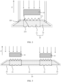
FIG. 1 is a schematic diagram of a module integrated with an optical sensor according to an embodiment of this application; -
FIG. 2 is a schematic diagram of another module integrated with an optical sensor according to an embodiment of this application; -
FIG. 3 is a schematic diagram of still another module integrated with an optical sensor according to an embodiment of this application; -
FIG. 4 is a schematic diagram of yet another module integrated with an optical sensor according to an embodiment of this application; -
FIG. 5 is a schematic diagram of still yet another module integrated with an optical sensor according to an embodiment of this application; -
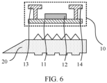
FIG. 6 is a schematic diagram of an optical sensor and a light guide plate according to an embodiment of this application; -
FIG. 7 is a schematic diagram of a display panel according to an embodiment of this application; -
FIG. 8 is a schematic diagram of another display panel according to an embodiment of this application; -
FIG. 9 is a schematic cross-sectional diagram corresponding toFIG. 7 ; -
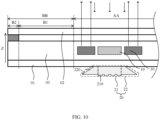
FIG. 10 is a schematic cross-sectional diagram corresponding toFIG. 8 ; -
FIG. 11 is another schematic cross-sectional diagram corresponding toFIG. 7 ; -
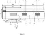
FIG. 12 is another schematic cross-sectional diagram corresponding toFIG. 8 ; -
FIG. 13 is a schematic cross-sectional diagram of a display panel according to an embodiment of this application; -
FIG. 14 is a schematic cross-sectional diagram of another display panel according to an embodiment of this application; -
FIG. 15 is a schematic cross-sectional diagram of still another display panel according to an embodiment of this application; and -
FIG. 16 is a schematic diagram of a display apparatus according to an embodiment of this application. - To better understand the technical solutions of this application, the following describes embodiments of this application in detail with reference to the accompanying drawings.
- It should be noted that the described embodiments are merely some but not all of embodiments of this application. Based on embodiments of this application, all other embodiments obtained by a person of ordinary skill in the art without creative efforts fall within the protection scope of this application.
- Terms used in embodiments of this application are merely for the purpose of describing specific embodiments, but are not intended to limit this application. Terms "a", "the", and "this" in singular forms in embodiments of this application and the appended claims are also intended to include plural forms, unless otherwise stated in the context clearly.
- It should be understood that the term "and/or" used in this specification is merely an association relationship for describing associated objects, and indicates that there may be three relationships. For example, A and/or B may indicate the following three cases: Only A exists, both A and B exist, and only B exists. In addition, the character "/" in this specification usually indicates an "or" relationship between the associated objects.
-
FIG. 1 is a schematic diagram of a module integrated with an optical sensor according to an embodiment of this application. - As shown in
FIG. 1 , the module integrated with theoptical sensor 10 provided in this embodiment of this application includes at least oneoptical sensor 10 and at least onelight guide plate 20. Thelight guide plate 20 and theoptical sensor 10 are arranged in a thickness direction Z of the module. Theoptical sensor 10 receives an optical signal from a first side of the module, and thelight guide plate 20 is disposed on a side that is of theoptical sensor 10 and that is away from the first side. For example, as shown inFIG. 1 , an upper side of the module is the first side of the module, and theoptical sensor 10 receives an optical signal transmitted from the upper side, and thelight guide plate 20 is disposed on a lower side of theoptical sensor 10. - In this embodiment of this application, the optical signal is a signal that is to be transmitted to the
optical sensor 10 and that is to be converted by theoptical sensor 10 into an electrical signal, to implement optical feature recognition, and may be specifically near-infrared light, infrared light, visible light, ultraviolet light, or the like. - The
light guide plate 20 includes afirst part 21 and asecond part 22. To be specific, thelight guide plate 20 is a continuous whole, and thelight guide plate 20 is divided into thefirst part 21 and thesecond part 22 based on different locations of thelight guide plate 20 and theoptical sensor 10. Thesecond part 22 does not overlap theoptical sensor 10 in the thickness direction Z of the module. In other words, thesecond part 22 is a part protruding from theoptical sensor 10. In addition, an included angle between at least apartial side edge 220 of thesecond part 22 and the thickness direction Z of the module is α, and α>0°. Thesecond part 22 is configured to receive an optical signal that is from the first side of the module and that is around theoptical sensor 10. In addition, a tilt angle of thepartial side edge 220 of thesecond part 22 is set to match a refractive index of thelight guide plate 20, to convert the received optical signal into light that can be totally reflected inside thelight guide plate 20. - The
light guide plate 20 is a material with a high refractive index. For example, when thelight guide plate 20 is made of an acrylic material, the refractive index of thelight guide plate 20 is 1.491. Based on a refractive index formula, when an optical signal that is incident on thelight guide plate 20 is totally reflected inside thelight guide plate 20, an incident angle of the optical signal needs to be greater than 41.8°. Based on this, the tilt angle of the at leastpartial side edge 220 of thesecond part 22 may be set. - The
first part 21 at least partially overlaps theoptical sensor 10 in the thickness direction Z of the module. In other words, at least a part of thefirst part 21 is blocked by theoptical sensor 10. In addition, a surface that is of thefirst part 21 and that is away from theoptical sensor 10 is afirst protrusion structure 210. Thefirst protrusion structure 210 may change a transmission path of light that is totally reflected inside thelight guide plate 20. In other words, thefirst protrusion structure 210 may damage total reflection of the light inside thelight guide plate 20, so that the light is emitted by thelight guide plate 20. In addition, because the surface that is of thefirst part 21 and that is away from theoptical sensor 10 is provided with thefirst protrusion structure 210, the optical signal whose transmission path is damaged inside thelight guide plate 20 is mainly emitted from a surface that is of thefirst part 21 and that is close to theoptical sensor 10, and mainly arrives at theoptical sensor 10. - The
first protrusion structure 210 may be specifically a printed white dot or an injection-molded small raised point. - In this embodiment of this application, the
second part 22 that protrudes from theoptical sensor 10 may receive an optical signal around theoptical sensor 10, and enable the optical signal to be totally reflected inside thelight guide plate 20. Thefirst part 21 that is blocked by theoptical sensor 10 may enable the optical signal inside thelight guide plate 20 to be emitted by thelight guide plate 20 after a total reflection path of the optical signal inside thelight guide plate 20 is changed, and to mainly arrive at theoptical sensor 10. In this embodiment of this application, thelight guide plate 20 is disposed below theoptical sensor 10, and thelight guide plate 20 is specially designed, so that intensity of an optical signal received by theoptical sensor 10 can be increased, and optical feature recognition precision of the module can be increased. - In an embodiment of this application, as shown in
FIG. 1 , thefirst protrusion structure 210 is disposed on only thefirst part 21 that overlaps theoptical sensor 10, and thefirst protrusion structure 210 is disposed on the surface that is of thefirst part 21 and that is away from theoptical sensor 10. In this case, an optical signal received by thelight guide plate 20 may be emitted from an area that is of thelight guide plate 20 and that corresponds to theoptical sensor 10, to effectively increase a signal quantity of optical signals received by theoptical sensor 10. -
FIG. 2 is a schematic diagram of another module integrated with anoptical sensor 10 according to an embodiment of this application. - In an embodiment of this application, as shown in
FIG. 2 , at least twosecond protrusion structures 211 are included on a side that is of afirst part 21 and that is close to theoptical sensor 10. Large-angle light exists in an optical signal that is transmitted inside alight guide plate 20 and whose total reflection path is damaged by afirst protrusion structure 210. Thesecond protrusion structure 211 may change an emission angle of the large-angle light, so that more light emitted by thelight guide plate 20 is incident on theoptical sensor 10. - In other words, the
second protrusion structure 211 may change a transmission path of a received optical signal, to specifically enable an emergent angle of the optical signal to be less than an incident angle. Thesecond protrusion structure 211 may be a prism structure such as a tapered structure or a hemispherical structure. Thesecond protrusion structure 211 may be made of acrylic resin. - It should be noted that, in this embodiment of this application, the
first protrusion structure 210 may be a part of thelight guide plate 20. To be specific, thefirst protrusion structure 210 is obtained by designing a surface that is of thefirst part 21 and that is away from theoptical sensor 10. Thesecond protrusion structure 211 may alternatively be a part of thelight guide plate 20. To be specific, thesecond protrusion structure 211 is obtained by designing a surface that is of thefirst part 21 and that is close to theoptical sensor 10. In addition, thesecond protrusion structure 211 may alternatively be a structure different from thelight guide plate 20. To be specific, thesecond protrusion structure 211 is additionally disposed on an upper surface that is of thelight guide plate 20 and that is close to theoptical sensor 10. -
FIG. 3 is a schematic diagram of still another module integrated with anoptical sensor 10 according to an embodiment of this application. - In an embodiment of this application, as shown in
FIG. 3 , the module includes a plurality ofoptical sensors 10, and alight guide plate 20 covers at least twooptical sensors 10 in a thickness direction Z of the module. In other words, onelight guide plate 20 corresponds to at least twooptical sensors 10. - In this embodiment, the
light guide plate 20 further includes athird part 23. Thethird part 23 covers an area between the at least twooptical sensors 10 in the thickness direction of the module. In other words, thethird part 23 of thelight guide plate 20 is a part located between adjacentfirst parts 21 that belong to a samelight guide plate 20. - The
first protrusion structure 210 does not overlap thethird part 23 in the thickness direction Z of the module. In other words, thefirst protrusion structure 210 is not disposed on athird part 23 that is of thelight guide plate 20 and that is located between adjacentoptical sensors 10, to prevent an optical signal received by thelight guide plate 20 from being emitted by thelight guide plate 20 from an area in which nooptical sensor 10 is disposed. - It can be understood that when the
light guide plate 20 covers the at least twooptical sensors 10, thelight guide plate 20 that covers the at least twooptical sensors 10 includes at least twofirst parts 21, and oneoptical sensor 10 corresponds to onefirst part 21. - In an implementation of this embodiment, the module includes one
light guide plate 20, and thelight guide plate 20 may be an entire-surface structure that covers alloptical sensors 10. -
FIG. 4 is a schematic diagram of yet another module integrated with anoptical sensor 10 according to an embodiment of this application. - In another embodiment of this application, as shown in
FIG. 4 , the module includes a plurality ofoptical sensors 10 and a plurality oflight guide plates 20, and theoptical sensors 10 and thelight guide plates 20 are disposed in a one-to-one correspondence. - In an implementation of this embodiment, as shown in
FIG. 4 , in theoptical sensor 10 and thelight guide plate 20 that are correspondingly disposed, a projection of thesecond part 22 surrounds a projection of theoptical sensor 10 in the thickness direction Z of the module, and an included angle between eachside edge 220 of thesecond part 22 and the thickness direction Z of the module is greater than 0°. In other words, all optical signals around theoptical sensor 10 may arrive at thelight guide plate 20, and are received and used by thelight guide plate 20. - In still another embodiment of this application, the module includes a plurality of
optical sensors 10 and a plurality oflight guide plates 20. In addition, at least one of thelight guide plates 20 covers at least twooptical sensors 10 in a thickness direction Z of the module, and the at least one of thelight guide plates 20 is disposed in a one-to-one correspondence with theoptical sensors 10.FIG. 5 is a schematic diagram of still yet another module integrated with anoptical sensor 10 according to an embodiment of this application. - In an embodiment of this application, as shown in
FIG. 5 , when the module includes at least twooptical sensors 10, the twooptical sensors 10 are disposed adjacent to each other and correspond to differentlight guide plates 20. In the twolight guide plates 20, an included angle between a thickness direction Z of the module and a side edge that is of onelight guide plate 20 and that is close to the otherlight guide plate 20 is basically equal to 0°. In other words, in a process error range, an included angle between the thickness direction Z of the module and a side edge located between twolight guide plates 20 in side edges of the twolight guide plates 20 that are disposed adjacent to each other is basically 0°. For example, as shown inFIG. 5 , a right side edge of a leftlight guide plate 20 is a side edge close to a rightlight guide plate 20, and the side edge is basically parallel to the thickness direction Z of the module; and a left side edge of the rightlight guide plate 20 is a side edge close to the leftlight guide plate 20, and the side edge is also basically parallel to the thickness direction Z of the module. In this way, crosstalk between optical signals above differentoptical sensors 10 can be avoided. -
FIG. 6 is a schematic diagram of anoptical sensor 10 and alight guide plate 20 according to an embodiment of this application. - In an embodiment of this application, as shown in
FIG. 6 , theoptical sensor 10 is a thin film transistor device, and theoptical sensor 10 includes anactive layer 11, agate 12, asource 13, and adrain 14. Theactive layer 11 may generate different carrier concentrations based on a quantity of received optical signals, so that theoptical sensor 10 generates different electrical signals, to implement optical feature recognition. Theactive layer 11 may be specifically at least one of an amorphous silicon film, a polycrystalline silicon film, or a metal oxide semiconductor layer. - In an implementation of this embodiment, the
gate 12 of the thin film transistor device that serves as theoptical sensor 10 is located on a side that is of theoptical sensor 10 and that is away from thelight guide plate 20. In other words, thegate 12 of the thin film transistor device that serves as theoptical sensor 10 is located on a side that is of the active layer and that receives an optical signal. In this case, thegate 12 blocks the optical signal, and a quantity of optical signals received by theoptical sensor 10 is affected. In this implementation, an inventive concept of this application is used. To be specific, thelight guide plate 20 provided in any one of the foregoing embodiments is disposed below theoptical sensor 10, to significantly increase a quantity of optical signals of a structure of theoptical sensor 10. - In this embodiment of this application, the
gate 12 of the thin film transistor device that serves as theoptical sensor 10 may be disposed in contact with theactive layer 11 of the thin film transistor device. In other words, no insulation layer is disposed between thegate 12 and theactive layer 11. In another embodiment of this application, theoptical sensor 10 may alternatively be at least one of an organic photosensitive device and a photodiode device. -
FIG. 7 is a schematic diagram of a display panel according to an embodiment of this application.FIG. 8 is a schematic diagram of another display panel according to an embodiment of this application.FIG. 9 is a schematic cross-sectional diagram corresponding toFIG. 7 .FIG. 10 is a schematic cross-sectional diagram corresponding toFIG. 8 . - An embodiment of this application further provides a display panel. As shown in
FIG. 7 to FIG. 10 , the display panel provided in this embodiment of this application includes a display area AA and a non-display area BB, and the non-display area BB surrounds the display area AA. The display area AA includes a plurality of light-emittingsubpixels 30, and the area is mainly configured to perform light-emitting display. The non-display area BB may further include a black frame area B2 and a middle area B1 located between the black frame area B2 and the display area AA. - At least one of the display area AAand the non-display area BB includes at least one
optical sensor 10 and at least onelight guide plate 20, and thelight guide plate 20 and theoptical sensor 10 are arranged in a thickness direction Z of the display panel. In other words, the display panel includes at least oneoptical sensor 10 and at least onelight guide plate 20, and the at least oneoptical sensor 10 and the at least onelight guide plate 20 are disposed in an area in which at least one of the display area AA and the non-display area BB is located. - For example, as shown in
FIG. 7 andFIG. 9 , theoptical sensor 10 and thelight guide plate 20 are disposed in the non-display area. In this case, theoptical sensor 10 may preferably serve as a device for ambient light detection or proximity light detection, to avoid impact of light emitted by the display area AA on ambient light detection or proximity light detection. - For example, as shown in
FIG. 8 andFIG. 10 , theoptical sensor 10 and thelight guide plate 20 are disposed in the display area AA. To be specific, the display area AA includes theoptical sensor 10, and theoptical sensor 10 located in the display area AA may be configured to perform biometric feature recognition, for example, fingerprint recognition. In a biometric feature recognition process, the light-emittingsubpixel 30 in the display area AA may serve as a detection light source for biometric feature recognition, and emit detection light to a biological object. Detection light reflected by the biological object is incident on theoptical sensor 10 and thelight guide plate 20, to implement biometric feature recognition. - For example, some
optical sensors 10 and somelight guide plates 20 are disposed in the non-display area BB, and the otheroptical sensors 10 and the otherlight guide plates 20 are disposed in the display area AA. - In addition, when at least some
optical sensors 10 and at least somelight guide plates 20 are disposed in the non-display area BB, theoptical sensors 10 and thelight guide plates 20 may be disposed in themiddle area B 1 as shown inFIG. 7 andFIG. 9 , or may be disposed in the black frame area B2, or may be partially disposed in the middle area B1 and partially disposed in the black frame area B2. - The
optical sensor 10 receives an optical signal from a first side of the display panel, and thelight guide plate 20 is disposed on a side that is of theoptical sensor 10 and that is away from the first side. For example, as shown inFIG. 9 andFIG. 10 , a side of a light-emitting surface of the display panel is the first side of the display panel. In this case, theoptical sensor 10 receives an optical signal transmitted from the side of the light-emitting surface of the display panel, and thelight guide plate 20 is disposed on a side that is of theoptical sensor 10 and that is away from the light-emitting surface of the display panel. - In this embodiment of this application, the optical signal is a signal that is to be transmitted to the
optical sensor 10 and that is to be converted by theoptical sensor 10 into an electrical signal, to implement optical feature recognition, and may be specifically near-infrared light, infrared light, visible light, ultraviolet light, or the like. - The
light guide plate 20 includes afirst part 21 and asecond part 22. To be specific, thelight guide plate 20 is a continuous whole, and thelight guide plate 20 is divided into thefirst part 21 and thesecond part 22 based on different locations of thelight guide plate 20 and the correspondingoptical sensor 10. - The
second part 22 does not overlap theoptical sensor 10 in the thickness direction Z of the display panel. In other words, thesecond part 22 is a part protruding from theoptical sensor 10. In addition, an included angle between at least apartial side edge 220 of thesecond part 22 and the thickness direction Z of the display panel is α, and α>0°. Thesecond part 22 is configured to receive an optical signal that is from the first side of the display panel and that is around theoptical sensor 10. In addition, a tilt angle of thepartial side edge 220 of thesecond part 22 is set to match a refractive index of thelight guide plate 20, to convert the received optical signal into light that may be totally reflected inside thelight guide plate 20. - The
light guide plate 20 is a material with a high refractive index. For example, when thelight guide plate 20 is made of an acrylic material, the refractive index of thelight guide plate 20 is 1.491. Based on a refractive index formula, when an optical signal that is incident on thelight guide plate 20 is totally reflected inside thelight guide plate 20, an incident angle of the optical signal needs to be greater than 41.8°. Based on this, the tilt angle of the at leastpartial side edge 220 of thesecond part 22 may be set. - The
first part 21 at least partially overlaps theoptical sensor 10 in the thickness direction Z of the display panel. In other words, at least a part of thefirst part 21 is blocked by theoptical sensor 10. In addition, a surface that is of thefirst part 21 and that is away from theoptical sensor 10 is afirst protrusion structure 210. Thefirst protrusion structure 210 may change a transmission path of light that is totally reflected inside thelight guide plate 20. In other words, thefirst protrusion structure 210 may damage total reflection of the light inside thelight guide plate 20, so that the light is emitted by thelight guide plate 20. In addition, because the surface that is of thefirst part 21 and that is away from theoptical sensor 10 is provided with thefirst protrusion structure 210, the optical signal whose transmission path is damaged inside thelight guide plate 20 is mainly emitted from a surface that is of thefirst part 21 and that is close to theoptical sensor 10, and mainly arrives at theoptical sensor 10. - The
first protrusion structure 210 may be specifically a printed white dot or an injection-molded small raised point. - In this embodiment of this application, the
second part 22 that protrudes from theoptical sensor 10 may receive an optical signal around theoptical sensor 10, and enable the optical signal to be totally reflected inside thelight guide plate 20. Thefirst part 21 that is blocked by theoptical sensor 10 may enable the optical signal inside thelight guide plate 20 to be emitted by thelight guide plate 20 after a total reflection path of the optical signal inside thelight guide plate 20 is changed, and to mainly arrive at theoptical sensor 10. In this embodiment of this application, thelight guide plate 20 is disposed below theoptical sensor 10, and thelight guide plate 20 is specially designed, so that intensity of an optical signal received by theoptical sensor 10 can be increased, and optical feature recognition precision of the display panel can be increased. - In this embodiment of this application, the display panel integrated with the
optical sensor 10 may implement biometric feature recognition (for example, fingerprint recognition or facial recognition), proximity light detection, ambient light detection, or the like. - In this embodiment of this application, in the thickness direction Z of the display panel, the display panel includes a
substrate 01, aprotective cover 02, and afunctional layer 03 located between thesubstrate 01 and theprotective cover 02. The light-emittingsubpixel 30 is disposed at thefunctional layer 03, and a photosensitive device may be integrated into thefunctional layer 03. Thesubstrate 01 may be a rigid substrate or a flexible substrate. - In addition, the
light guide plate 20 may be attached to a side that is of thesubstrate 01 and that is away from thefunctional layer 03, or may be attached to a side that is of theprotective cover 02 and that is away from thefunctional layer 03. When an optical signal received by the photosensitive device comes from a side that is of the display panel and that is close to theprotective cover 02, thelight guide plate 20 may be attached to the side that is of thesubstrate 01 and that is away from thefunctional layer 03. When an optical signal received by the photosensitive device comes from a side that is of the display panel and that is close to thesubstrate 01, thelight guide plate 20 may be attached to the side that is of theprotective cover 02 and that is away from thefunctional layer 03. - In an implementation, as shown in
FIG. 9 andFIG. 10 , a display manner of the display panel is top emission, and the photosensitive device receives the optical signal on the side of the light-emitting surface of the display panel. In other words, a side on which theprotective cover 02 is located is the light-emitting surface of the display panel, and the photosensitive device receives the optical signal from the side of the light-emitting surface of the display panel. In this case, thelight guide plate 20 may be attached to thesubstrate 01. -
FIG. 11 is another schematic cross-sectional diagram corresponding toFIG. 7 .FIG. 12 is another schematic cross-sectional diagram corresponding toFIG. 8 . - In an embodiment of this application, as shown in
FIG. 11 andFIG. 12 , at least twosecond protrusion structures 211 are included on a side that is of thefirst part 21 and that is close to theoptical sensor 10. Large-angle light exists in an optical signal that is transmitted inside thelight guide plate 20 and whose total reflection path is damaged by thefirst protrusion structure 210. Thesecond protrusion structure 211 may change an emission angle of the large-angle light, so that more light emitted by thelight guide plate 20 is incident on theoptical sensor 10. - A specific structure, material, and disposing manner of the
second protrusion structure 211 may be the same as a specific structure and disposing manner of thesecond protrusion structure 211 in the module integrated with theoptical sensor 10 in the foregoing embodiments, and details are not described herein again. -
FIG. 13 is a schematic cross-sectional diagram of a display panel according to an embodiment of this application. - In an embodiment of this application, as shown in
FIG. 13 , a non-display area BB includes a plurality ofoptical sensors 10, and in a thickness direction Z of the display panel, alight guide plate 20 covers at least twooptical sensors 10 located on two opposite sides of a display area AA. In other words, at least oneoptical sensor 10 is disposed in each of non-display areas BB located on two opposite sides of the display area AA, and optical devices respectively disposed in the non-display areas BB on the two opposite sides may be covered by a samelight guide plate 20. - In this embodiment, the
light guide plate 20 further includes athird part 23, and at least a part of thethird part 23 is located in the display area AA. In the thickness direction Z of the display panel, afirst protrusion structure 210 does not overlap thethird part 23 located in the display area AA. In other words, thefirst protrusion structure 210 is not disposed on a part that is of thelight guide plate 20 and that is located in the display area AA, so that an optical signal received by thelight guide plate 20 can be prevented from being emitted by thelight guide plate 20 in the display area AA. A waste caused when the optical signal received by thelight guide plate 20 is not used for optical feature recognition is avoided. In addition, impact exerted, on a normal display picture in the display area AA, when an optical signal used for optical feature recognition is emitted from the display area AA is avoided. - In addition, a
second protrusion structure 211 does not overlap thethird part 23. - It can be understood that when the
light guide plate 20 covers the at least twooptical sensors 10, thelight guide plate 20 that covers the at least twooptical sensors 10 includes at least twofirst parts 21, and oneoptical sensor 10 corresponds to onefirst part 21. - In an implementation of this embodiment, the display panel includes one
light guide plate 20, and thelight guide plate 20 may be an entire-surface structure that covers alloptical sensors 10. - In another embodiment of this application, the display panel includes a plurality of
optical sensors 10 and a plurality oflight guide plates 20, and theoptical sensors 10 and thelight guide plates 20 are disposed in a one-to-one correspondence. - In an implementation of this application, in the
optical sensor 10 and thelight guide plate 20 that are correspondingly disposed, a projection of asecond part 22 surrounds a projection of theoptical sensor 10 in the thickness direction Z of the display panel, and an included angle between eachside edge 220 of thesecond part 22 and the thickness direction Z of the display panel is greater than 0°. In other words, all optical signals around theoptical sensor 10 may arrive at thelight guide plate 20, and are received and used by thelight guide plate 20, to effectively increase a signal quantity of optical signals received by theoptical sensor 10. - In still another embodiment of this application, the display panel includes a plurality of
optical sensors 10 and a plurality oflight guide plates 20. In addition, at least one of thelight guide plates 20 covers at least twooptical sensors 10 in a thickness direction Z of the display panel, and the at least one of thelight guide plates 20 is disposed in a one-to-one correspondence with theoptical sensors 10. -
FIG. 14 is a schematic cross-sectional diagram of another display panel according to an embodiment of this application. - In an embodiment of this application, as shown in
FIG. 14 , a non-display area BB includes at least oneoptical sensor 10 and at least onelight guide plate 20, and a side edge that is of thelight guide plate 20 disposed in the non-display area BB and that is close to a display area AA is parallel to a thickness direction of the display panel. In other words, in a process error range, an included angle between the thickness direction Z of the display panel and the side edge close to the display area AA in side edges of thelight guide plate 20 disposed in the non-display area BB is basically 0°. For example, as shown inFIG. 14 , a right side edge of thelight guide plate 20 disposed in the non-display area BB is a side edge close to the display area AA, and the side edge is basically parallel to the thickness direction Z of the display panel. - Therefore, when light that is emitted by the display panel and that is used to perform light-emitting display arrives at the non-display area BB, a case in which the light is emitted to the
optical sensor 10 after being totally reflected inside thelight guide plate 20 basically does not occur, to avoid impact of the light for light-emitting display in the display area AA on optical feature recognition accuracy of the non-display area BB. -
FIG. 15 is a schematic cross-sectional diagram of still another display panel according to an embodiment of this application. - In an embodiment of this application, as shown in
FIG. 15 , anoptical sensor 10 is a thin film transistor device, and theoptical sensor 10 includes anactive layer 11, agate 12, asource 13, and adrain 14. Theactive layer 11 may generate different carrier concentrations based on a quantity of received optical signals, so that theoptical sensor 10 generates different electrical signals, to implement optical feature recognition. Theactive layer 11 may be specifically at least one of an amorphous silicon film, a polycrystalline silicon film, or a metal oxide semiconductor layer. - In an implementation of this embodiment, the
gate 12 of the thin film transistor device that serves as theoptical sensor 10 is located on a side that is of theoptical sensor 10 and that is away from alight guide plate 20. In other words, thegate 12 of the thin film transistor device that serves as theoptical sensor 10 is located on a side that is of the active layer and that receives an optical signal. In this case, thegate 12 blocks the optical signal, and a quantity of optical signals received by theoptical sensor 10 is affected. In this implementation, an inventive concept of this application is used. To be specific, thelight guide plate 20 provided in any one of the foregoing embodiments is disposed below theoptical sensor 10, to significantly increase a quantity of optical signals of a structure of theoptical sensor 10. - Further, the thin film transistor device that serves as the
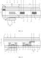
optical sensor 10 may be manufactured at a same layer as at least a part of a structure of a thinfilm transistor device 301 in a light-emittingsubpixel 30. The thinfilm transistor device 301 in the light-emittingsubpixel 30 may provide a light emitting signal for alight emitting device 302 in the light-emittingsubpixel 30. As shown inFIG. 15 , thegate 12 of the thin film transistor device that serves as theoptical sensor 10 may be disposed at a same layer as thegate 32 of the thinfilm transistor device 301 in the light-emittingsubpixel 30, and thesource 13 and thedrain 14 of the thin film transistor device that serves as theoptical sensor 10 may be disposed at a same layer as thesource 33 and thedrain 34 of the thinfilm transistor device 301 in the light-emittingsubpixel 30. - The
active layer 11 of the thin film transistor device that serves as theoptical sensor 10 and theactive layer 31 of the thinfilm transistor device 301 in the light-emittingsubpixel 30 may be disposed at a same layer or disposed at different layers. In addition, in this embodiment of this application, thegate 12 of the thin film transistor device that serves as theoptical sensor 10 may be disposed in contact with theactive layer 11 of the thin film transistor device. In other words, no insulation layer is disposed between thegate 12 and theactive layer 11. - In another embodiment of this application, the
optical sensor 10 may alternatively be at least one of an organic photosensitive device and a photodiode device. - This application further provides a display apparatus.
FIG. 16 is a schematic diagram of a display apparatus according to an embodiment of this application. In an embodiment of this application, as shown inFIG. 16 , the display apparatus includes adisplay panel 001 provided in any embodiment of this application. A specific structure of thedisplay panel 001 has been described in detail in the foregoing embodiments. Details are not described herein again. Certainly, the display apparatus shown inFIG. 16 is provided only for schematic illustration. For example, the display apparatus may be any display apparatus with a display function, for example, a mobile phone, a tablet computer, a notebook computer, an E-book, a television, or a smartwatch; or the display panel. - The foregoing descriptions are merely specific implementations of this application, and any change or replacement readily figured out by a person skilled in the art within the technical scope disclosed in this application shall fall within the protection scope of this application. The protection scope of this application shall be subject to the protection scope of the claims.
Claims (17)
- A module integrated with an optical sensor, comprising:at least one optical sensor, wherein the optical sensor receives an optical signal from a first side of the module; andat least one light guide plate, wherein the light guide plate and the optical sensor are arranged in a thickness direction of the module, and the light guide plate is disposed on a side that is of the optical sensor and that is away from the first side, whereinthe light guide plate comprises a first part and a second part; and in the thickness direction of the module, the first part at least partially overlaps the optical sensor, and the second part does not overlap the optical sensor; anda surface that is of the first part and that is away from the optical sensor is a first protrusion structure, and an included angle between at least a partial side edge of the second part and the thickness direction of the module is greater than 0°.
- The module according to claim 1, wherein at least two second protrusion structures are comprised on a side that is of the first part and that is close to the optical sensor.
- The module according to claim 1, wherein the module comprises a plurality of optical sensors; and in the thickness direction of the module, the light guide plate covers at least two optical sensors;the light guide plate further comprises a third part; and in the thickness direction of the module, the third part covers an area between the at least two optical sensors; andthe first protrusion structure does not overlap the third part in the thickness direction of the module.
- The module according to claim 1, wherein the module comprises a plurality of optical sensors and a plurality of light guide plates, and the optical sensors and the light guide plates are disposed in a one-to-one correspondence.
- The module according to claim 4, wherein in the optical sensor and the light guide plate that are correspondingly disposed, a projection of the second part surrounds a projection of the optical sensor in the thickness direction of the module; and
an included angle between each side edge of the second part and the thickness direction of the module is greater than 0°. - The module according to claim 1, wherein the optical sensor is a thin film transistor device, and a gate of the thin film transistor device is located on a side that is of the optical sensor and that is away from the light guide plate.
- The module according to claim 1, wherein the optical sensor is at least one of an organic photosensitive device and a photodiode device.
- A display panel, comprising a display area and a non-display area, wherein the non-display area surrounds the display area, and at least one of the display area and the non-display area comprises:at least one optical sensor, wherein the optical sensor receives an optical signal from a first side of the display panel; andat least one light guide plate, wherein the light guide plate and the optical sensor are arranged in a thickness direction of the display panel, and the light guide plate is disposed on a side that is of the optical sensor and that is away from the first side, whereinthe light guide plate comprises a first part and a second part; and in the thickness direction of the display panel, the first part at least partially overlaps the optical sensor, and the second part does not overlap the optical sensor; anda surface that is of the first part and that is away from the optical sensor is a first protrusion structure, and an included angle between at least a partial side edge of the second part and the thickness direction of the display panel is greater than 0°.
- The display panel according to claim 8, wherein at least two second protrusion structures are comprised on a side that is of the first part and that is close to the optical sensor.
- The display panel according to claim 8, wherein the non-display area comprises a plurality of optical sensors;in the thickness direction of the display panel, the light guide plate covers at least two optical sensors located on two opposite sides of the display area;the light guide plate further comprises a third part, and at least a part of the third part is located in the display area; andin the thickness direction of the display panel, the first protrusion structure does not overlap the third part located in the display area.
- The display panel according to claim 8, wherein the display panel comprises a plurality of optical sensors and a plurality of light guide plates, and the optical sensors and the light guide plates are disposed in a one-to-one correspondence.
- The display panel according to claim 11, wherein in the optical sensor and the light guide plate that are correspondingly disposed, a projection of the second part surrounds a projection of the optical sensor in the thickness direction of the display panel; and
an included angle between each side edge of the second part and the thickness direction of the display panel is greater than 0°. - The display panel according to claim 8, wherein the non-display area comprises at least one optical sensor and at least one light guide plate; and
a side edge that is of the light guide plate disposed in the non-display area and that is close to the display area is parallel to the thickness direction of the display panel. - The display panel according to claim 8, wherein the display area comprises the optical sensor, and the optical sensor located in the display area is configured to perform biometric feature recognition.
- The display panel according to claim 8, wherein the optical sensor is a thin film transistor device, and a gate of the thin film transistor device is located on a side that is of an active layer and that is away from the light guide plate.
- The display panel according to claim 8, wherein the optical sensor is at least one of an organic photosensitive device and a photodiode device.
- A display apparatus, comprising the display panel according to any one of claims 8 to 16.
Applications Claiming Priority (2)
| Application Number | Priority Date | Filing Date | Title |
|---|---|---|---|
| CN202111264791.5A CN115019353B (en) | 2021-10-28 | 2021-10-28 | Modules, display panels, and display devices integrating optical sensors |
| PCT/CN2022/113332 WO2023071445A1 (en) | 2021-10-28 | 2022-08-18 | Module integrated with optical sensor, display panel, and display apparatus |
Publications (3)
| Publication Number | Publication Date |
|---|---|
| EP4261795A1 true EP4261795A1 (en) | 2023-10-18 |
| EP4261795A4 EP4261795A4 (en) | 2024-07-24 |
| EP4261795B1 EP4261795B1 (en) | 2025-06-25 |
Family
ID=83065168
Family Applications (1)
| Application Number | Title | Priority Date | Filing Date |
|---|---|---|---|
| EP22885345.3A Active EP4261795B1 (en) | 2021-10-28 | 2022-08-18 | Module integrated with optical sensor, display panel, and display apparatus |
Country Status (4)
| Country | Link |
|---|---|
| US (1) | US12175789B2 (en) |
| EP (1) | EP4261795B1 (en) |
| CN (1) | CN115019353B (en) |
| WO (1) | WO2023071445A1 (en) |
Family Cites Families (20)
| Publication number | Priority date | Publication date | Assignee | Title |
|---|---|---|---|---|
| CN101620025A (en) * | 2009-05-05 | 2010-01-06 | 华映光电股份有限公司 | Display optical detection device and display optical detection method |
| CN102644890B (en) * | 2012-04-01 | 2013-11-20 | 深圳市华星光电技术有限公司 | Narrow-frame backlight module |
| US9140930B2 (en) * | 2012-04-01 | 2015-09-22 | Shenzhen China Star Optoelectronics Technology Co., Ltd. | Slim frame backlight module |
| JP6355066B2 (en) * | 2013-08-29 | 2018-07-11 | 株式会社リコー | Sensor device and image forming apparatus |
| CN106951816A (en) * | 2016-01-07 | 2017-07-14 | 上海箩箕技术有限公司 | Optical fingerprint sensor module |
| CN205880271U (en) * | 2016-07-25 | 2017-01-11 | 深圳Tcl新技术有限公司 | Light guide plate and backlight module |
| CN109074495A (en) | 2017-01-04 | 2018-12-21 | 深圳市汇顶科技股份有限公司 | Improve the optical sensing performance of optical sensor module under the screen for shielding upper fingerprint sensing |
| US10529759B2 (en) * | 2017-09-11 | 2020-01-07 | Pixart Imaging Inc. | Optical sensor package module and manufacturing method thereof |
| CN108258017B (en) * | 2018-01-02 | 2021-05-14 | 上海天马微电子有限公司 | Display panel and display device |
| CN109037296B (en) * | 2018-08-07 | 2021-02-05 | 武汉天马微电子有限公司 | Display device and electronic equipment |
| CN109618025B (en) * | 2018-11-20 | 2021-01-12 | 维沃移动通信有限公司 | Electronic equipment |
| CN109447046B (en) | 2018-12-27 | 2021-07-23 | 厦门天马微电子有限公司 | Display panels and display devices |
| CN110515231B (en) | 2019-08-30 | 2021-11-23 | 厦门天马微电子有限公司 | Display device |
| US11380129B2 (en) * | 2019-09-04 | 2022-07-05 | Beijing Boe Optoelectronics Technology Co., Ltd. | Texture recognition device and display device |
| CN213210660U (en) * | 2020-04-15 | 2021-05-14 | 深圳阜时科技有限公司 | Backlight module, passive light-emitting display device, under-screen biological characteristic detection system and electronic equipment |
| CN111965897B (en) * | 2020-08-26 | 2022-07-12 | 厦门天马微电子有限公司 | Backlight module and display device |
| CN112485947B (en) * | 2020-12-09 | 2022-08-16 | 武汉天马微电子有限公司 | Display module and display device |
| CN112882288B (en) * | 2021-03-12 | 2022-09-09 | 厦门天马微电子有限公司 | Display device |
| CN113301190B (en) * | 2021-04-16 | 2022-08-05 | 荣耀终端有限公司 | Pressure sensor and electronic device |
| CN113296314B (en) * | 2021-06-01 | 2022-07-12 | 厦门天马微电子有限公司 | Display module and display device |
-
2021
- 2021-10-28 CN CN202111264791.5A patent/CN115019353B/en active Active
-
2022
- 2022-08-18 EP EP22885345.3A patent/EP4261795B1/en active Active
- 2022-08-18 US US18/262,639 patent/US12175789B2/en active Active
- 2022-08-18 WO PCT/CN2022/113332 patent/WO2023071445A1/en not_active Ceased
Also Published As
| Publication number | Publication date |
|---|---|
| WO2023071445A9 (en) | 2023-07-13 |
| WO2023071445A1 (en) | 2023-05-04 |
| US12175789B2 (en) | 2024-12-24 |
| CN115019353A (en) | 2022-09-06 |
| EP4261795A4 (en) | 2024-07-24 |
| US20240304024A1 (en) | 2024-09-12 |
| CN115019353B (en) | 2023-05-09 |
| EP4261795B1 (en) | 2025-06-25 |
Similar Documents
| Publication | Publication Date | Title |
|---|---|---|
| EP3396588B1 (en) | Display screen, display device and mobile terminal | |
| US10503952B2 (en) | Fingerprint identification display device | |
| US9620571B2 (en) | Electronic devices with light sensors and displays | |
| US10691916B1 (en) | Pattern recognition device, array substrate and display apparatus | |
| US11003886B2 (en) | Display apparatus including a fingerprint identification device | |
| US8570303B2 (en) | Display module | |
| US10592722B2 (en) | Photosensitive unit, photosensitive module and display device | |
| US20210357614A1 (en) | Terminal device | |
| US8325156B2 (en) | Optical touch screen device | |
| WO2021087742A1 (en) | Under-screen fingerprint recognition apparatus, lcd fingerprint recognition system, and electronic device | |
| US11308308B2 (en) | Fingerprint recognition device, recognition device and display device | |
| US12279505B2 (en) | Display device and touch controller | |
| US11569290B2 (en) | Sensing device and display apparatus including the same | |
| CN109037296B (en) | Display device and electronic equipment | |
| WO2021012117A1 (en) | Under-screen optical fingerprint recognition apparatus and system, diffusion film, and liquid crystal display | |
| CN212163464U (en) | Optical sensing device and electronic apparatus | |
| US20160231774A1 (en) | Display module | |
| KR20190027475A (en) | Flat Panel Display Embedding Optical Imaging Sensor | |
| CN114740994B (en) | Display screen and display device | |
| EP4047656B1 (en) | Optical sensing device | |
| CN111586267A (en) | Optical sensing devices and electronic equipment | |
| US20230181067A1 (en) | In-cell optical biometrics sensor | |
| KR102911080B1 (en) | Display modules and electronic devices | |
| US12175789B2 (en) | Module integrated with optical sensor, display panel, and display apparatus | |
| US20230074241A1 (en) | Electronic device |
Legal Events
| Date | Code | Title | Description |
|---|---|---|---|
| STAA | Information on the status of an ep patent application or granted ep patent |
Free format text: STATUS: THE INTERNATIONAL PUBLICATION HAS BEEN MADE |
|
| PUAI | Public reference made under article 153(3) epc to a published international application that has entered the european phase |
Free format text: ORIGINAL CODE: 0009012 |
|
| STAA | Information on the status of an ep patent application or granted ep patent |
Free format text: STATUS: REQUEST FOR EXAMINATION WAS MADE |
|
| 17P | Request for examination filed |
Effective date: 20230712 |
|
| AK | Designated contracting states |
Kind code of ref document: A1 Designated state(s): AL AT BE BG CH CY CZ DE DK EE ES FI FR GB GR HR HU IE IS IT LI LT LU LV MC MK MT NL NO PL PT RO RS SE SI SK SM TR |
|
| A4 | Supplementary search report drawn up and despatched |
Effective date: 20240625 |
|
| RIC1 | Information provided on ipc code assigned before grant |
Ipc: G02B 6/42 20060101ALI20240619BHEP Ipc: H10K 59/60 20230101ALI20240619BHEP Ipc: G06V 10/94 20220101ALI20240619BHEP Ipc: G06V 40/13 20220101AFI20240619BHEP |
|
| GRAP | Despatch of communication of intention to grant a patent |
Free format text: ORIGINAL CODE: EPIDOSNIGR1 |
|
| STAA | Information on the status of an ep patent application or granted ep patent |
Free format text: STATUS: GRANT OF PATENT IS INTENDED |
|
| DAV | Request for validation of the european patent (deleted) | ||
| DAX | Request for extension of the european patent (deleted) | ||
| INTG | Intention to grant announced |
Effective date: 20250117 |
|
| GRAS | Grant fee paid |
Free format text: ORIGINAL CODE: EPIDOSNIGR3 |
|
| GRAA | (expected) grant |
Free format text: ORIGINAL CODE: 0009210 |
|
| STAA | Information on the status of an ep patent application or granted ep patent |
Free format text: STATUS: THE PATENT HAS BEEN GRANTED |
|
| AK | Designated contracting states |
Kind code of ref document: B1 Designated state(s): AL AT BE BG CH CY CZ DE DK EE ES FI FR GB GR HR HU IE IS IT LI LT LU LV MC MK MT NL NO PL PT RO RS SE SI SK SM TR |
|
| REG | Reference to a national code |
Ref country code: GB Ref legal event code: FG4D |
|
| REG | Reference to a national code |
Ref country code: CH Ref legal event code: EP |
|
| REG | Reference to a national code |
Ref country code: DE Ref legal event code: R096 Ref document number: 602022016627 Country of ref document: DE |
|
| REG | Reference to a national code |
Ref country code: CH Ref legal event code: EP |
|
| REG | Reference to a national code |
Ref country code: IE Ref legal event code: FG4D |
|
| REG | Reference to a national code |
Ref country code: NL Ref legal event code: FP |
|
| PGFP | Annual fee paid to national office [announced via postgrant information from national office to epo] |
Ref country code: NL Payment date: 20250716 Year of fee payment: 4 |
|
| PG25 | Lapsed in a contracting state [announced via postgrant information from national office to epo] |
Ref country code: FI Free format text: LAPSE BECAUSE OF FAILURE TO SUBMIT A TRANSLATION OF THE DESCRIPTION OR TO PAY THE FEE WITHIN THE PRESCRIBED TIME-LIMIT Effective date: 20250625 |
|
| PGFP | Annual fee paid to national office [announced via postgrant information from national office to epo] |
Ref country code: DE Payment date: 20250708 Year of fee payment: 4 |
|
| REG | Reference to a national code |
Ref country code: LT Ref legal event code: MG9D |
|
| PG25 | Lapsed in a contracting state [announced via postgrant information from national office to epo] |
Ref country code: NO Free format text: LAPSE BECAUSE OF FAILURE TO SUBMIT A TRANSLATION OF THE DESCRIPTION OR TO PAY THE FEE WITHIN THE PRESCRIBED TIME-LIMIT Effective date: 20250925 Ref country code: GR Free format text: LAPSE BECAUSE OF FAILURE TO SUBMIT A TRANSLATION OF THE DESCRIPTION OR TO PAY THE FEE WITHIN THE PRESCRIBED TIME-LIMIT Effective date: 20250926 |
|
| PG25 | Lapsed in a contracting state [announced via postgrant information from national office to epo] |
Ref country code: BG Free format text: LAPSE BECAUSE OF FAILURE TO SUBMIT A TRANSLATION OF THE DESCRIPTION OR TO PAY THE FEE WITHIN THE PRESCRIBED TIME-LIMIT Effective date: 20250625 |
|
| PG25 | Lapsed in a contracting state [announced via postgrant information from national office to epo] |
Ref country code: HR Free format text: LAPSE BECAUSE OF FAILURE TO SUBMIT A TRANSLATION OF THE DESCRIPTION OR TO PAY THE FEE WITHIN THE PRESCRIBED TIME-LIMIT Effective date: 20250625 |
|
| PGFP | Annual fee paid to national office [announced via postgrant information from national office to epo] |
Ref country code: AT Payment date: 20251020 Year of fee payment: 4 |
|
| PG25 | Lapsed in a contracting state [announced via postgrant information from national office to epo] |
Ref country code: RS Free format text: LAPSE BECAUSE OF FAILURE TO SUBMIT A TRANSLATION OF THE DESCRIPTION OR TO PAY THE FEE WITHIN THE PRESCRIBED TIME-LIMIT Effective date: 20250925 |
|
| PG25 | Lapsed in a contracting state [announced via postgrant information from national office to epo] |
Ref country code: LV Free format text: LAPSE BECAUSE OF FAILURE TO SUBMIT A TRANSLATION OF THE DESCRIPTION OR TO PAY THE FEE WITHIN THE PRESCRIBED TIME-LIMIT Effective date: 20250625 |
|
| PG25 | Lapsed in a contracting state [announced via postgrant information from national office to epo] |
Ref country code: PT Free format text: LAPSE BECAUSE OF FAILURE TO SUBMIT A TRANSLATION OF THE DESCRIPTION OR TO PAY THE FEE WITHIN THE PRESCRIBED TIME-LIMIT Effective date: 20251027 |
|
| REG | Reference to a national code |
Ref country code: AT Ref legal event code: MK05 Ref document number: 1807350 Country of ref document: AT Kind code of ref document: T Effective date: 20250625 |
|
| PG25 | Lapsed in a contracting state [announced via postgrant information from national office to epo] |
Ref country code: IS Free format text: LAPSE BECAUSE OF FAILURE TO SUBMIT A TRANSLATION OF THE DESCRIPTION OR TO PAY THE FEE WITHIN THE PRESCRIBED TIME-LIMIT Effective date: 20251025 |
|
| PG25 | Lapsed in a contracting state [announced via postgrant information from national office to epo] |
Ref country code: AT Free format text: LAPSE BECAUSE OF FAILURE TO SUBMIT A TRANSLATION OF THE DESCRIPTION OR TO PAY THE FEE WITHIN THE PRESCRIBED TIME-LIMIT Effective date: 20250625 Ref country code: SM Free format text: LAPSE BECAUSE OF FAILURE TO SUBMIT A TRANSLATION OF THE DESCRIPTION OR TO PAY THE FEE WITHIN THE PRESCRIBED TIME-LIMIT Effective date: 20250625 |
|
| PG25 | Lapsed in a contracting state [announced via postgrant information from national office to epo] |
Ref country code: CZ Free format text: LAPSE BECAUSE OF FAILURE TO SUBMIT A TRANSLATION OF THE DESCRIPTION OR TO PAY THE FEE WITHIN THE PRESCRIBED TIME-LIMIT Effective date: 20250625 |
|
| PG25 | Lapsed in a contracting state [announced via postgrant information from national office to epo] |
Ref country code: PL Free format text: LAPSE BECAUSE OF FAILURE TO SUBMIT A TRANSLATION OF THE DESCRIPTION OR TO PAY THE FEE WITHIN THE PRESCRIBED TIME-LIMIT Effective date: 20250625 |
|
| PG25 | Lapsed in a contracting state [announced via postgrant information from national office to epo] |
Ref country code: EE Free format text: LAPSE BECAUSE OF FAILURE TO SUBMIT A TRANSLATION OF THE DESCRIPTION OR TO PAY THE FEE WITHIN THE PRESCRIBED TIME-LIMIT Effective date: 20250625 |
|
| PG25 | Lapsed in a contracting state [announced via postgrant information from national office to epo] |
Ref country code: SK Free format text: LAPSE BECAUSE OF FAILURE TO SUBMIT A TRANSLATION OF THE DESCRIPTION OR TO PAY THE FEE WITHIN THE PRESCRIBED TIME-LIMIT Effective date: 20250625 |
|
| PG25 | Lapsed in a contracting state [announced via postgrant information from national office to epo] |
Ref country code: ES Free format text: LAPSE BECAUSE OF FAILURE TO SUBMIT A TRANSLATION OF THE DESCRIPTION OR TO PAY THE FEE WITHIN THE PRESCRIBED TIME-LIMIT Effective date: 20250625 |
|
| PG25 | Lapsed in a contracting state [announced via postgrant information from national office to epo] |
Ref country code: RO Free format text: LAPSE BECAUSE OF FAILURE TO SUBMIT A TRANSLATION OF THE DESCRIPTION OR TO PAY THE FEE WITHIN THE PRESCRIBED TIME-LIMIT Effective date: 20250625 |
|
| REG | Reference to a national code |
Ref country code: CH Ref legal event code: H13 Free format text: ST27 STATUS EVENT CODE: U-0-0-H10-H13 (AS PROVIDED BY THE NATIONAL OFFICE) Effective date: 20260324 |
|
| REG | Reference to a national code |
Ref country code: DE Ref legal event code: R097 Ref document number: 602022016627 Country of ref document: DE |
|
| PG25 | Lapsed in a contracting state [announced via postgrant information from national office to epo] |
Ref country code: MC Free format text: LAPSE BECAUSE OF FAILURE TO SUBMIT A TRANSLATION OF THE DESCRIPTION OR TO PAY THE FEE WITHIN THE PRESCRIBED TIME-LIMIT Effective date: 20250625 |
|
| PG25 | Lapsed in a contracting state [announced via postgrant information from national office to epo] |
Ref country code: DK Free format text: LAPSE BECAUSE OF FAILURE TO SUBMIT A TRANSLATION OF THE DESCRIPTION OR TO PAY THE FEE WITHIN THE PRESCRIBED TIME-LIMIT Effective date: 20250625 |
|
| PG25 | Lapsed in a contracting state [announced via postgrant information from national office to epo] |
Ref country code: LU Free format text: LAPSE BECAUSE OF NON-PAYMENT OF DUE FEES Effective date: 20250818 Ref country code: IT Free format text: LAPSE BECAUSE OF FAILURE TO SUBMIT A TRANSLATION OF THE DESCRIPTION OR TO PAY THE FEE WITHIN THE PRESCRIBED TIME-LIMIT Effective date: 20250625 |
|
| PG25 | Lapsed in a contracting state [announced via postgrant information from national office to epo] |
Ref country code: CH Free format text: LAPSE BECAUSE OF NON-PAYMENT OF DUE FEES Effective date: 20250831 |
|
| PLBE | No opposition filed within time limit |
Free format text: ORIGINAL CODE: 0009261 |
|
| STAA | Information on the status of an ep patent application or granted ep patent |
Free format text: STATUS: NO OPPOSITION FILED WITHIN TIME LIMIT |
|
| REG | Reference to a national code |
Ref country code: CH Ref legal event code: L10 Free format text: ST27 STATUS EVENT CODE: U-0-0-L10-L00 (AS PROVIDED BY THE NATIONAL OFFICE) Effective date: 20260507 |