EP4261550A1 - Redundancy circuit - Google Patents
Redundancy circuit Download PDFInfo
- Publication number
- EP4261550A1 EP4261550A1 EP23163828.9A EP23163828A EP4261550A1 EP 4261550 A1 EP4261550 A1 EP 4261550A1 EP 23163828 A EP23163828 A EP 23163828A EP 4261550 A1 EP4261550 A1 EP 4261550A1
- Authority
- EP
- European Patent Office
- Prior art keywords
- scan
- flop
- flip
- input
- output
- Prior art date
- Legal status (The legal status is an assumption and is not a legal conclusion. Google has not performed a legal analysis and makes no representation as to the accuracy of the status listed.)
- Granted
Links
Images


Classifications
-
- G—PHYSICS
- G01—MEASURING; TESTING
- G01R—MEASURING ELECTRIC VARIABLES; MEASURING MAGNETIC VARIABLES
- G01R31/00—Arrangements for testing electric properties; Arrangements for locating electric faults; Arrangements for electrical testing characterised by what is being tested not provided for elsewhere
- G01R31/28—Testing of electronic circuits, e.g. by signal tracer
- G01R31/317—Testing of digital circuits
- G01R31/3181—Functional testing
- G01R31/3185—Reconfiguring for testing, e.g. LSSD, partitioning
- G01R31/318533—Reconfiguring for testing, e.g. LSSD, partitioning using scanning techniques, e.g. LSSD, Boundary Scan, JTAG
-
- H—ELECTRICITY
- H03—ELECTRONIC CIRCUITRY
- H03K—PULSE TECHNIQUE
- H03K19/00—Logic circuits, i.e. having at least two inputs acting on one output; Inverting circuits
- H03K19/20—Logic circuits, i.e. having at least two inputs acting on one output; Inverting circuits characterised by logic function, e.g. AND, OR, NOR, NOT circuits
- H03K19/23—Majority or minority circuits, i.e. giving output having the state of the majority or the minority of the inputs
-
- G—PHYSICS
- G01—MEASURING; TESTING
- G01R—MEASURING ELECTRIC VARIABLES; MEASURING MAGNETIC VARIABLES
- G01R31/00—Arrangements for testing electric properties; Arrangements for locating electric faults; Arrangements for electrical testing characterised by what is being tested not provided for elsewhere
- G01R31/28—Testing of electronic circuits, e.g. by signal tracer
- G01R31/317—Testing of digital circuits
- G01R31/3181—Functional testing
- G01R31/31816—Soft error testing; Soft error rate evaluation; Single event testing
-
- G—PHYSICS
- G01—MEASURING; TESTING
- G01R—MEASURING ELECTRIC VARIABLES; MEASURING MAGNETIC VARIABLES
- G01R31/00—Arrangements for testing electric properties; Arrangements for locating electric faults; Arrangements for electrical testing characterised by what is being tested not provided for elsewhere
- G01R31/28—Testing of electronic circuits, e.g. by signal tracer
- G01R31/317—Testing of digital circuits
- G01R31/3181—Functional testing
- G01R31/3185—Reconfiguring for testing, e.g. LSSD, partitioning
- G01R31/318522—Test of Sequential circuits
- G01R31/318525—Test of flip-flops or latches
-
- G—PHYSICS
- G01—MEASURING; TESTING
- G01R—MEASURING ELECTRIC VARIABLES; MEASURING MAGNETIC VARIABLES
- G01R31/00—Arrangements for testing electric properties; Arrangements for locating electric faults; Arrangements for electrical testing characterised by what is being tested not provided for elsewhere
- G01R31/28—Testing of electronic circuits, e.g. by signal tracer
- G01R31/317—Testing of digital circuits
- G01R31/3181—Functional testing
- G01R31/3185—Reconfiguring for testing, e.g. LSSD, partitioning
- G01R31/318533—Reconfiguring for testing, e.g. LSSD, partitioning using scanning techniques, e.g. LSSD, Boundary Scan, JTAG
- G01R31/318536—Scan chain arrangements, e.g. connections, test bus, analog signals
-
- G—PHYSICS
- G01—MEASURING; TESTING
- G01R—MEASURING ELECTRIC VARIABLES; MEASURING MAGNETIC VARIABLES
- G01R31/00—Arrangements for testing electric properties; Arrangements for locating electric faults; Arrangements for electrical testing characterised by what is being tested not provided for elsewhere
- G01R31/28—Testing of electronic circuits, e.g. by signal tracer
- G01R31/317—Testing of digital circuits
- G01R31/3181—Functional testing
- G01R31/3185—Reconfiguring for testing, e.g. LSSD, partitioning
- G01R31/318533—Reconfiguring for testing, e.g. LSSD, partitioning using scanning techniques, e.g. LSSD, Boundary Scan, JTAG
- G01R31/318544—Scanning methods, algorithms and patterns
-
- G—PHYSICS
- G01—MEASURING; TESTING
- G01R—MEASURING ELECTRIC VARIABLES; MEASURING MAGNETIC VARIABLES
- G01R31/00—Arrangements for testing electric properties; Arrangements for locating electric faults; Arrangements for electrical testing characterised by what is being tested not provided for elsewhere
- G01R31/28—Testing of electronic circuits, e.g. by signal tracer
- G01R31/317—Testing of digital circuits
- G01R31/3181—Functional testing
- G01R31/3185—Reconfiguring for testing, e.g. LSSD, partitioning
- G01R31/318533—Reconfiguring for testing, e.g. LSSD, partitioning using scanning techniques, e.g. LSSD, Boundary Scan, JTAG
- G01R31/318566—Comparators; Diagnosing the device under test
-
- G—PHYSICS
- G01—MEASURING; TESTING
- G01R—MEASURING ELECTRIC VARIABLES; MEASURING MAGNETIC VARIABLES
- G01R31/00—Arrangements for testing electric properties; Arrangements for locating electric faults; Arrangements for electrical testing characterised by what is being tested not provided for elsewhere
- G01R31/28—Testing of electronic circuits, e.g. by signal tracer
- G01R31/317—Testing of digital circuits
- G01R31/3181—Functional testing
- G01R31/3185—Reconfiguring for testing, e.g. LSSD, partitioning
- G01R31/318533—Reconfiguring for testing, e.g. LSSD, partitioning using scanning techniques, e.g. LSSD, Boundary Scan, JTAG
- G01R31/318594—Timing aspects
-
- H—ELECTRICITY
- H03—ELECTRONIC CIRCUITRY
- H03K—PULSE TECHNIQUE
- H03K19/00—Logic circuits, i.e. having at least two inputs acting on one output; Inverting circuits
- H03K19/0021—Modifications of threshold
-
- H—ELECTRICITY
- H03—ELECTRONIC CIRCUITRY
- H03K—PULSE TECHNIQUE
- H03K19/00—Logic circuits, i.e. having at least two inputs acting on one output; Inverting circuits
- H03K19/20—Logic circuits, i.e. having at least two inputs acting on one output; Inverting circuits characterised by logic function, e.g. AND, OR, NOR, NOT circuits
-
- H—ELECTRICITY
- H03—ELECTRONIC CIRCUITRY
- H03K—PULSE TECHNIQUE
- H03K3/00—Circuits for generating electric pulses; Monostable, bistable or multistable circuits
- H03K3/02—Generators characterised by the type of circuit or by the means used for producing pulses
- H03K3/027—Generators characterised by the type of circuit or by the means used for producing pulses by the use of logic circuits, with internal or external positive feedback
- H03K3/037—Bistable circuits
Definitions
- the present disclosure relates generally to an electronic system and method, and, in particular embodiments, to a redundancy circuit.
- Integrated circuits are generally tested for faults.
- Logic circuits are commonly tested using a method often referred to as scan testing.
- scan testing patterns are shifted in through one or more chains of flip-flops (also referred to as a scan chains) to stimulate one or more logic circuits. Results from the stimulated logic circuits are loaded into the scan chains and are shifted out for evaluation.
- expected patterns based on proper functionality of the one or more logic circuits
- no faults are detected and the circuit may be treated as defect-free.
- the shifted out patterns do not match the expected patterns, then faults are detected.
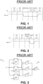
- Figure 1 shows exemplary launch-on-capture (LOC) waveforms of scan chain clock signal clk and scan enable signal scan_en.
- LOC launch-on-capture
- the second pulse of clock signal clk causes the loading of the outputs of the stimulated logic circuits into flip-flops of the scan chain. Once scan enable signal scan_en transitions to the high state, data in the scan chain shifts out each time clock signal clk pulses. The data shifted out is then evaluated for faults.
- the launch and capture clock pulses may be performed at-speed so that the logic circuits are tested for faults related to transition delays.
- LOC testing allows for shifting data into or out of the scan chain at slow speed while still performing at-speed testing of the logic circuits.
- LOC testing may allow for an easier implementation of the scan circuit (compared with LOS testing) since the scan enable signal scan_en transition may be slow.
- Figure 2 shows exemplary launch-on-shift (LOS) waveforms of scan chain clock signal clk and scan enable signal scan_en.
- LOS testing is very similar to LOC testing. However, LOS testing performs the launch operation during the last shift pulse of clock signal clk.
- scan enable signal scan_en transitions to the low state after the last shift pulse of clock signal clk but before the capture pulse of clock signal clk.
- LOS testing may be performed at-speed.
- the scan enable signal scan_en implementation is designed to transition fast enough to allow for at-speed testing during LOS.
- LOS testing may allow for lower test time (compared with LOC testing) since LOS testing uses the clock pulse for the last shift for both shifting data through the scan chain and for the launch operation.
- Scan testing may be implemented in an automated test equipment (ATE), where, e.g., the ATE provides the test vectors to the IC and evaluates the results (data shifted out) for determining faults.
- ATE automated test equipment
- Scan testing may also be performed as a logic built-in-self-test (LBIST), where the IC applies the test vectors to itself (e.g., using a pseudorandom number generator) and determines whether a fault occurred by using an LBIST controller of the IC.
- LBIST logic built-in-self-test
- Scan testing and/or the performance of LBIST may provide a way of detecting the presence of faults.
- a circuit is expected to continue proper operation even in the presence of a fault.
- a redundancy circuit may be used. This is typically true for safety sensitive automotive applications.
- Security features may also demand logic redundancy around critical bits, e.g., to prevent against adversary attacks.
- a redundancy circuit may be understood as a fault tolerant circuit in which the circuit is capable of continued and proper operation in the presence of a fault.
- FIG. 3 shows a schematic diagram of exemplary triple-voting flop (TVF) 300, which is an example of a redundancy circuit.
- Triple-voting flop 300 includes D-flip-flops 302, 304, and 306, and voting circuit 318.
- Voting circuit 318 includes AND gates 310, 312, and 314, and OR gate 320.
- Triple-voting flop 300 uses majority voting to determine output D out . For example, when all D-flip-flops 302, 304, and 306 are operating properly, the content of each of D-flip-flops 302, 304, and 306 is the same, and the output D out is equal to the content of D-flip-flops 302, 304, and 306. If one of D-flip-flops 302, 304, or 306 outputs a wrong state, output D out continues to output the correct value (since the two other D-flip-flops of D-flip-flops 302, 304, and 306 output the correct value).
- D-flip-flops 302 and 304 output a logic 1 and D-flip-flop 306 flips and outputs a logic o
- the output of AND gate 310 is a logic 1
- the output of each of AND gates 312 and 314 is a logic o
- the output of OR gate 320 is a logic 1.
- D-flip-flops 302 and 304 output a logic 0 and D-flip-flop 306 flips and outputs a logic 1
- the output of each of AND gates 310, 312 and 314 is a logic o
- the output of OR gate 320 is a logic 0.
- Triple-voting flops may be used for safety sensitive bits, where an accidental flip of the bit (e.g., due to a soft error) cannot be tolerated.
- triple-voting flop 300 may replace a D-flip-flop where redundancy of such D-flip-flop is desired.
- an integrated circuit includes: a voting circuit including N scan flip-flops, where N is an odd number greater than or equal to 3, and where the N scan flip-flops includes a first scan flip-flop and a second scan flip-flop, where an output of the first scan flip-flop is coupled to a scan input of the second scan flip-flop; a scan chain including the N scan flip-flops of the voting circuit, and third and fourth scan flip-flops, the scan chain configured to receive a scan enable signal; and a scan enable control circuit configured to control a scan enable input of the first or second scan flip-flops based on the scan enable signal and based on a scan input of the third scan flip-flop or an output of the fourth scan flip-flop.
- an integrated circuit includes: a triple-voting flop including first, second, and third scan flip-flops, where an output of the first scan flip-flop is coupled to a scan input of the second scan flip-flop, and where an output of the second scan flip-flop is coupled to a scan input of the third scan flip-flop; a scan chain configured to receive a scan enable signal, the scan chain including the first, second, and third scan flip-flops of the triple-voting flop, the scan chain further including a fourth and a fifth scan flip-flops; and a scan enable control circuit configured to control a scan enable input of the first or third scan flip-flops based on the scan enable signal and based on a scan input of the fourth scan flip-flop or an output of the fifth scan flip-flop.
- a method for testing a triple-voting flop includes: providing a scan enable signal to a scan chain that includes first, second, third, fourth, fifth, and sixth scan flip-flops, where the triple-voting flop includes the first, second, and third scan flip-flops, where an output of the first scan flip-flop is coupled to a scan input of the second scan flip-flop, where an output of the second scan flip-flop is coupled to a scan input of the third scan flip-flop, and where an output of the third scan flip-flop is coupled to a scan input of the sixth scan flip-flop; providing a scan input signal to the scan chain; controlling a scan enable input of the first scan flip-flop based on the scan enable signal and based on a scan input of the fourth scan flip-flop; controlling a scan enable input of the third scan flip-flop based on the scan enable signal and based on an output of the fifth scan flip-flop; receiving a scan output signal from the scan chain; and determining whether there is a fault in the triple
- references to "an embodiment” in this description indicate that a particular configuration, structure or feature described in relation to the embodiment is included in at least one embodiment. Consequently, phrases such as "in one embodiment” that may appear at different points of the present description do not necessarily refer exactly to the same embodiment. Furthermore, specific formations, structures or features may be combined in any appropriate manner in one or more embodiments. Embodiments of the present invention will be described in specific contexts, e.g., a triple-voting flop capable of improved scan coverage, e.g., for automotive applications. Some embodiments may be implemented with other types of voting flops, such as with N-voting flops, where N is an odd number greater than 3. Some embodiments may be implemented in applications other than automotive, such as industrial applications, space applications, or any other applications that could benefit from improved scan coverage of a voting flop.
- Figure 4 shows exemplary triple-voting flop 400 with scan flip flops.
- Triple-voting flop 400 is structurally similar to triple-voting flop 300.
- Triple-voting flop 400 replaces D-flip-flops 302, 304, and 306 with scan flip-flops 402, 404, and 406, respectively.
- An additional scan flip-flop 410 is used to capture the output of OR gate 320.
- scan flip-flops 402, 404, 406, and 410 are connected to form a portion of scan chain 420.
- each of scan flip-flops 402, 404, 406, and 410 is as follows.
- the scan enable input SE is deasserted (e.g., low)
- the scan flip-flop latches the content of its D input and outputs it at its output Q during each clock pulse of clock signal clk.
- the scan enable input SE is asserted (e.g., high)
- the scan flip-flop latches the content at the scan in input SI and outputs it at the output Q during each pulse of clock clk.
- each of scan flip-flops 402, 404, 406, and 410 latches the content at the respective D input and outputs it at the respective Q output during each pulse of clock clk.
- scan enable signal scan_en is asserted (e.g., high)
- each of scan flip-flops 402, 404, 406, and 410 latches the content at the respective SI input and outputs it at the respective Q output during each pulse of clock clk.
- triple-voting flop 400 operates in similar manner as triple-voting flop 300.
- scan chain 420 implements LOC
- data e.g., a test pattern
- scan flip-flops 402, 404, and 406 latch the same content of input D in and outputs it in their respective outputs Q.
- the output of OR gate 320 is captured by scan flip-flop 410. Such output is then shifted out with further shift pulses and then may be compared with the expected output to determine if a fault of triple-voting flop 400 exists.
- triple-voting flop 400 may achieve a fault coverage greater than 50% of triple-voting flop 400.
- scan flip-flop 402 is slow to rise but scan flip-flops 404 and 406 are operating properly, such slow-to-rise fault of scan flip-flop 402 is masked by the presence of logic 1 at outputs of scan flip-flops 404 and 406. Thus, a slow-to-rise fault at scan flip-flop 402 may be undetectable.
- scan chain 420 implements LOS
- data is first loaded into scan flip-flops 402, 404, and 406 (during the shift pulses) from scan input signal scan_in.
- the content of each scan flip-flops 402, 404, and 406 is outputted at their respective outputs Q.
- the output of OR gate 320 is captured by scan flip-flop 410. Such output may then be compared with the expected output to determine if a fault of triple-voting flop 400 exists.
- triple-voting flop 400 may achieve a fault coverage greater than 80% of triple-voting flop 400.
- Such operation causes that during the last shift/launch pulse, scan flip-flop 402 transitions from a logic 1 to a logic o, and the output of scan flip-flops 404 and 406 remain a logic 1, which causes the output of OR gate 320 to remain a 1.
- scan flip-flop 402 is slow-to-fall but scan flip-flops 404 and 406 are operating properly, such slow-to-fall fault of scan flip-flop 402 is masked and may be undetectable.
- a triple-voting flop is advantageously capable of improved coverage (e.g., 100% at-speed and stuck-at coverage) using LOC scan.
- the triple-voting flop includes first, second, and third scan flip-flops connected in a chain.
- a first logic circuit gates the scan enable input SE of the first scan flip-flop based on a scan input SI of a preceding scan flip-flop of the scan chain.
- a second logic circuit gates the scan enable input SE of the third scan flip-flop based on an output Q of a subsequent scan flip-flop of the scan chain.
- some embodiments are advantageously capable of selectively disabling the scan enable input SE of the first and third scan flip-flops, thereby allowing flexibility to load independent values to the first, second, and third scan flip-flops, thereby allowing improved (e.g., at-speed) scan coverage of the first, second, and third scan flip-flops.
- some embodiments advantageously allow for an easier implementation of the scan circuit (compared with LOS testing) since the scan enable signal scan_en transition may be slow.
- Figure 5 shows a schematic diagram of triple-voting flop 500, according to an embodiment of the present invention.
- Triple-voting flop 500 includes scan flip-flops 402, 404, 406, voting circuit 318, and scan enable control circuits 550 and 552.
- Scan enable control circuit 550 includes AND gate 546 and OR gate 542.
- Scan enable control circuit 552 includes AND gate 548 and OR gate 544.
- scan flip-flops 402, 404, 406, and 410 are connected to form a portion of scan chain 520, where scan chain 520 further includes scan flip-flops 532 and 534.
- scan enable signal scan_en is kept low
- trans_mode signal is kept low
- triple-voting flop 500 operates in similar manner as triple-voting flop 300.
- scan chain 520 implements LOC.
- the scan enable input SE of each of scan flip-flops 402, 404, 406, and 408 receives scan enable signal scan_en, and thus, operates in a similar manner as triple-voting flop 400 when triple-voting flop 400 operates with LOC.
- the scan enable inputs SE of scan flip-flops 402 and 406 are selectively controlled based on the scan input SI of scan flip-flop 532 and the output Q of scan flip-flop 534, respectively.
- the content of scan flip-flops 402, 404, and 406 is independently controlled using trans_mode signal to achieve improved (e.g., at-speed) scan coverage, e.g., compared with triple-voting flop 400.
- at-speed testing using LOC it is possible to test a slow-to-rise fault at the output of scan flip-flop 402.
- scan flip-flops 402, 404, and 406 are loaded with logic o.
- the scan test pattern is designed such that the scan in input SI of scan flip-flop 532 is low and the output Q of scan flip-flop 534 is high while trans_mode signal is high.
- the scan enable input SE of scan flip-flops 402 and 404 is low and the scan enable input SE of scan flip-flop 406 is high.
- input D in provides a logic 1 to all scan flip-flops 402, 404, and 406. Since, the scan enable input SE of scan flip-flop 406 is low, the output Q of scan flip-flop 406 remains a logic 0 while the outputs Q of scan flip-flops 402 and 404 transition from low to high.
- scan test patterns can be designed, e.g., manually or with the aid of a conventional automated test pattern generator (ATPG), to advantageously achieve up to 100% stuck-at scan coverage and 100% at-speed scan coverage for triple-voting flop 500.
- AVG automated test pattern generator
- all transitions (rising or falling) over every node of voting circuit 318 is tested to ensure that each transition occurs within a predetermined time.
- the additional logic e.g., 542, 544, 546, and 548 introduced in triple-voting flop 500 is fully covered by scan (e.g., using scan flip-flops 402, 404, and 406 to capture the outputs of OR gates 542 and 544).
- the trans_mode signal is kept static (with the same value) through the execution of one or more (or all) scan test pattern (the trans_mode signal may have different states in different scan patterns, but may not change during the execution of each of the one or more (or all) scan test pattern).
- triple-voting flop 500 is implemented as part of an integrated circuit (IC). In some embodiments, scan test of triple-voting flop 500 is performed using an ATE (e.g., during production testing of the IC). In some embodiments, scan test of triple-voting flop 500 is performed using LBIST.
- IC integrated circuit
- scan test of triple-voting flop 500 is performed using an ATE (e.g., during production testing of the IC). In some embodiments, scan test of triple-voting flop 500 is performed using LBIST.
- the output Q of scan flip-flop 532 may be connected to the scan input SI of scan flip-flop 402. In some embodiments, there may be additional scan flip-flops coupled between the output Q of scan flip-flop 532 and the scan in input SI of scan flip-flop 402.
- the output Q of scan flip-flop 410 may be connected to the scan input SI of scan flip-flop 534. In some embodiments, there may be additional scan flip-flops coupled between the output Q of scan flip-flop 410 and the scan in input SI of scan flip-flop 534.
- scan flip-flops 402, 404, 406, 410, 532, and 534 may be implemented in any way known in the art.
- a triple-voting flop with improved scan coverage may be implemented with voting circuit 318, as shown in Figure 5 .
- a triple-voting flop with improved scan coverage may be implemented with different voting circuits.
- Figure 6 shows a schematic diagram of triple-voting flop 600, according to an embodiment of the present invention. Triple-voting flop 600 operates in a similar manner as triple-voting flop 500. Triple-voting flop 500, however, replaces voting circuit 318 with voting circuit 618. In some embodiments, triple-voting flop 600 is capable of achieving improved (e.g., 100% at-speed and stuck-at coverage) using LOC scan in a similar manner as triple-voting flop 500.
- Advantages of some embodiments include the capability of achieving improved scan coverage of a triple-voting flop with no impact on the functional path of the triple-voting flop (e.g., from the D input of scan flip-flops 402, 404, and 406 to the output of OR gate 320), and with no impact to scan-stitching. Some embodiments achieve the improved scan coverage with low area impact (e.g., only 4 logic gates added to the triple-voting flop). In some embodiments, the improved scan coverage of the triple-voting flop is achieved without routing fast signals (e.g., since scan is performed using LOC, and thus, scan enable signal scan_en may be a relatively slow signal, and since the trans_mode signal may be a static signal during scan testing).
- fast signals e.g., since scan is performed using LOC, and thus, scan enable signal scan_en may be a relatively slow signal, and since the trans_mode signal may be a static signal during scan testing.
- Figure 7 shows a schematic diagram of IC 700, according to an embodiment of the present invention.
- IC 700 includes scan chain 720 and scan controller 730.
- Scan chain 720 includes scan flip-flops 702, 704, 402, 404, 406, and 708.
- IC 700 also includes triple-voting flop 706, which includes scan flip-flops 402, 404, and 406, and scan enable control circuits 550 and 552.
- triple-voting flop 706 may be implemented as triple-voting flop 500 or 600.
- scan enable control circuit 550 receives trans_mode signal, scan enable signal scan_en, and a control signal from a scan input SI of preceding scan flip-flop (704) and controls the scan enable input SE of scan flip-flop 402 based on the received signals.
- Scan enable control circuit 552 receives trans_mode signal, scan enable signal scan_en, and a control signal from an output Q of a subsequent scan flip-flop (708) and controls the scan enable input SE of scan flip-flop 406 based on the received signals.
- scan enable control circuit 550 may receive its control signal from a scan input SI or output Q of another scan flip-flop of scan chain 720, such as another scan flip-flop preceding triple-voting flop 706 or a scan flip-flop subsequent to triple voting flop 706.
- scan enable control circuit 552 may receive its control signal from a scan input SI or output Q of another scan flip-flop of scan chain 720, such as another scan flip-flop preceding triple-voting flop 706 or a scan flip-flop subsequent to triple voting flop 706.
- scan controller 730 performs LBIST by generating signals scan_en, trans_mode, and scan_in, testing triple-voting flop 706 using LOC, receiving signal scan_out, and determining whether a fault exist in triple-voting flop 706 based on output signal scan_out.
- an ATE generates signals scan_in, scan_en, and trans_mode, receives signal scan_out, and determines whether a fault exist in voting circuit 706 based on signal scan_out.
- scan controller 730 may be implemented using digital circuits, such as with a finite state machine. In some embodiments, scan controller 730 may be implemented with a generic or custom micro-controller or processor coupled to a memory. Other implementations may also be possible.
- Example 1 An integrated circuit including: a voting circuit including N scan flip-flops, where N is an odd number greater than or equal to 3, and where the N scan flip-flops includes a first scan flip-flop and a second scan flip-flop, where an output of the first scan flip-flop is coupled to a scan input of the second scan flip-flop; a scan chain including the N scan flip-flops of the voting circuit, and third and fourth scan flip-flops, the scan chain configured to receive a scan enable signal; and a scan enable control circuit configured to control a scan enable input of the first or second scan flip-flops based on the scan enable signal and based on a scan input of the third scan flip-flop or an output of the fourth scan flip-flop.
- a voting circuit including N scan flip-flops, where N is an odd number greater than or equal to 3
- the N scan flip-flops includes a first scan flip-flop and a second scan flip-flop, where an output of the first scan flip-flop is coupled to a scan input of the second scan flip-
- Example 2 The integrated circuit of example 1, where the scan enable control circuit is configured to control the scan enable input of the first or second scan flip-flops based on the scan input of the third scan flip-flop or the output of the fourth scan flip-flop when a further signal is asserted.
- Example 3 The integrated circuit of one of examples 1 or 2, where the scan enable control circuit is configured to control the scan enable input of the first and second scan flip-flops with the scan enable signal when the further signal is deasserted.
- Example 4 The integrated circuit of one of examples 1 to 3, where the scan enable control circuit includes a first OR gate having an output coupled to the scan enable input of the first or second scan flip-flops, a first input configured to receive the scan enable signal, and a second input coupled to the scan input of the third scan flip-flop or to the output of the fourth scan flip-flop.
- Example 5 The integrated circuit of one of examples 1 to 4, where the scan enable control circuit further includes a first AND gate having an output coupled to a second input of the first OR gate, a first input coupled to the scan input of the third scan flip-flop or to the output of the fourth scan flip-flop, and a second input configured to receive a further signal.
- Example 6 The integrated circuit of one of examples 1 to 5, where the first input of the first AND gate is coupled to the scan input of the third scan flip-flop, and where the output of the first OR gate is coupled to the scan enable input of the first scan flip-flop, the scan enable control circuit further including: a second OR gate having an output coupled to the scan enable input of the second scan flip-flop, and a first input configured to receive the scan enable signal; and a second AND gate having an output coupled to a second input of the second OR gate, a first input coupled to the output of the fourth scan flip-flop, and a second input configured to receive the further signal.
- Example 7 The integrated circuit of one of examples 1 to 6, further including a scan controller configured to provide the scan enable signal to the scan chain.
- Example 8 The integrated circuit of one of examples 1 to 7, where, when the integrated circuit is in scan mode, the scan controller is configured to provide a scan input signal to the scan chain, receive a scan output signal from the scan chain, and determine whether there is a fault in the voting circuit based on the scan output signal.
- Example 9 The integrated circuit of one of examples 1 to 8, where the second scan flip-flop is a last scan flip-flop of the N scan flip-flops of the voting circuit.
- Example 10. The integrated circuit of one of examples 1 to 9, where an output of the second scan flip-flop is coupled to a scan input of the fourth scan flip-flop.
- Example 11. The integrated circuit of one of examples 1 to 10, where an output of the third scan flip-flop is coupled to a scan input of the first scan flip-flop.
- Example 12 The integrated circuit of one of examples 1 to 11, where the output of the third scan flip-flop is directly connected to the scan input of the first scan flip-flop.
- Example 13 The integrated circuit of one of examples 1 to 12, where N is equal to 3.
- Example 14 An integrated circuit including: a triple-voting flop including first, second, and third scan flip-flops, where an output of the first scan flip-flop is coupled to a scan input of the second scan flip-flop, and where an output of the second scan flip-flop is coupled to a scan input of the third scan flip-flop; a scan chain configured to receive a scan enable signal, the scan chain including the first, second, and third scan flip-flops of the triple-voting flop, the scan chain further including a fourth and a fifth scan flip-flops; and a scan enable control circuit configured to control a scan enable input of the first or third scan flip-flops based on the scan enable signal and based on a scan input of the fourth scan flip-flop or an output of the fifth scan flip-flop.
- Example 15 The integrated circuit of example 14, where the triple-voting flop includes: a first AND gate having a first input coupled to the output of the first scan flip-flop, and a second input coupled to the output of the second scan flip-flop; a second AND gate having a first input coupled to the output of the second scan flip-flop, and a second input coupled to an output of the third scan flip-flop; a third AND gate having a first input coupled to the output of the first scan flip-flop, and a second input coupled to the output of the third scan flip-flop; and an OR gate having a first input coupled to an output of the first AND gate, a second input coupled to an output of the second AND gate, and a third input coupled to an output of the third AND gate.
- Example 16 The integrated circuit of one of examples 14 or 15, where triple-voting flop includes: a first OR gate having a first input coupled to the output of the first scan flip-flop, and a second input coupled to the output of the second scan flip-flop; a second OR gate having a first input coupled to the output of the second scan flip-flop, and a second input coupled to an output of the third scan flip-flop; a third OR gate having a first input coupled to the output of the first scan flip-flop, and a second input coupled to the output of the third scan flip-flop; and an AND gate having a first input coupled to an output of the first OR gate, a second input coupled to an output of the second OR gate, and a third input coupled to an output of the third OR gate.
- Example 17 A method for testing a triple-voting flop, the method including: providing a scan enable signal to a scan chain that includes first, second, third, fourth, fifth, and sixth scan flip-flops, where the triple-voting flop includes the first, second, and third scan flip-flops, where an output of the first scan flip-flop is coupled to a scan input of the second scan flip-flop, where an output of the second scan flip-flop is coupled to a scan input of the third scan flip-flop, and where an output of the third scan flip-flop is coupled to a scan input of the sixth scan flip-flop; providing a scan input signal to the scan chain; controlling a scan enable input of the first scan flip-flop based on the scan enable signal and based on a scan input of the fourth scan flip-flop; controlling a scan enable input of the third scan flip-flop based on the scan enable signal and based on an output of the fifth scan flip-flop; receiving a scan output signal from the scan chain; and determining whether there is a fault in the triple-vo
- Example 18 The method of example 17, further including providing a further signal to the scan chain, where controlling the scan enable input of the first scan flip-flop is further based on the further signal, and where controlling the scan enable input of the third scan flip-flop is further based on the further signal.
- Example 19 The method of one of examples 17 or 18, further including: asserting the scan enable signal; asserting the further signal; providing a clock signal to the scan chain; while the scan enable and further signals are asserted, pulsing the clock signal to shift into the scan chain a first test pattern based on the scan input signal; after shifting the first test pattern into the scan chain and while keeping the further signal asserted, deasserting the scan enable signal and pulsing the clock signal twice to capture an output of the triple-voting flop with the sixth scan flip-flop; and after capturing the output of the triple-voting flop, asserting the scan enable signal and pulsing the clock signal to generate the scan output signal.
- Example 20 The method of one of examples 17 to 19, where determining whether there is a fault in the triple-voting flop includes verifying that all rising and falling transitions of every output node of the triple-voting flop occur within a predetermined time.
Landscapes
- Engineering & Computer Science (AREA)
- General Engineering & Computer Science (AREA)
- Physics & Mathematics (AREA)
- General Physics & Mathematics (AREA)
- Computer Hardware Design (AREA)
- Computing Systems (AREA)
- Mathematical Physics (AREA)
- Microelectronics & Electronic Packaging (AREA)
- Tests Of Electronic Circuits (AREA)
Abstract

Description
- The present disclosure relates generally to an electronic system and method, and, in particular embodiments, to a redundancy circuit.
- Integrated circuits (ICs) are generally tested for faults. Logic circuits are commonly tested using a method often referred to as scan testing. During scan testing, patterns are shifted in through one or more chains of flip-flops (also referred to as a scan chains) to stimulate one or more logic circuits. Results from the stimulated logic circuits are loaded into the scan chains and are shifted out for evaluation. When the shifted out patterns match expected patterns (based on proper functionality of the one or more logic circuits), then no faults are detected and the circuit may be treated as defect-free. When the shifted out patterns do not match the expected patterns, then faults are detected.
-
Figure 1 shows exemplary launch-on-capture (LOC) waveforms of scan chain clock signal clk and scan enable signal scan_en. As shown inFigure 1 , when scan_en is in a high state (also referred to as high, or logic 1), data (also referred to as test vectors, test patterns, vectors, or patterns) shifts into the scan chain each time clock signal clk pulses. When scan enable signal scan_en transitions to a low state (also referred to as low, or logic o), the first pulse of clock signal clk causes the logic circuits having inputs coupled to the scan chain to transition in a step generally referred to as launch. The second pulse of clock signal clk causes the loading of the outputs of the stimulated logic circuits into flip-flops of the scan chain. Once scan enable signal scan_en transitions to the high state, data in the scan chain shifts out each time clock signal clk pulses. The data shifted out is then evaluated for faults. The launch and capture clock pulses may be performed at-speed so that the logic circuits are tested for faults related to transition delays. - As can be seen in
Figure 1 , LOC testing allows for shifting data into or out of the scan chain at slow speed while still performing at-speed testing of the logic circuits. Thus, in some implementations, LOC testing may allow for an easier implementation of the scan circuit (compared with LOS testing) since the scan enable signal scan_en transition may be slow. -
Figure 2 shows exemplary launch-on-shift (LOS) waveforms of scan chain clock signal clk and scan enable signal scan_en. As shown, LOS testing is very similar to LOC testing. However, LOS testing performs the launch operation during the last shift pulse of clock signal clk. Thus, as shown inFigure 2 , scan enable signal scan_en transitions to the low state after the last shift pulse of clock signal clk but before the capture pulse of clock signal clk. - In a similar manner as in LOC testing, LOS testing may be performed at-speed. Thus, in some implementations, the scan enable signal scan_en implementation is designed to transition fast enough to allow for at-speed testing during LOS.
- As can be seen in
Figure 2 , in some implementations, LOS testing may allow for lower test time (compared with LOC testing) since LOS testing uses the clock pulse for the last shift for both shifting data through the scan chain and for the launch operation. - Scan testing, e.g., with implementations as illustrated in
Figures 1 and 2 , may be implemented in an automated test equipment (ATE), where, e.g., the ATE provides the test vectors to the IC and evaluates the results (data shifted out) for determining faults. Scan testing may also be performed as a logic built-in-self-test (LBIST), where the IC applies the test vectors to itself (e.g., using a pseudorandom number generator) and determines whether a fault occurred by using an LBIST controller of the IC. - Scan testing and/or the performance of LBIST may provide a way of detecting the presence of faults.
- In some applications, a circuit is expected to continue proper operation even in the presence of a fault. In such applications, a redundancy circuit may be used. This is typically true for safety sensitive automotive applications. Security features may also demand logic redundancy around critical bits, e.g., to prevent against adversary attacks.
- A redundancy circuit may be understood as a fault tolerant circuit in which the circuit is capable of continued and proper operation in the presence of a fault.
-
Figure 3 shows a schematic diagram of exemplary triple-voting flop (TVF) 300, which is an example of a redundancy circuit. Triple-voting flop 300 includes D-flip-flops voting circuit 318.Voting circuit 318 includes ANDgates gate 320. - Triple-
voting flop 300 uses majority voting to determine output Dout. For example, when all D-flip-flops flops flops flops flops flops flop 306 flips and outputs a logic o, the output ofAND gate 310 is a logic 1, the output of each ofAND gates gate 320 is a logic 1. If D-flip-flops flop 306 flips and outputs a logic 1, the output of each ofAND gates OR gate 320 is a logic 0. - Triple-voting flops may be used for safety sensitive bits, where an accidental flip of the bit (e.g., due to a soft error) cannot be tolerated. For example, triple-
voting flop 300 may replace a D-flip-flop where redundancy of such D-flip-flop is desired. - In accordance with an embodiment, an integrated circuit includes: a voting circuit including N scan flip-flops, where N is an odd number greater than or equal to 3, and where the N scan flip-flops includes a first scan flip-flop and a second scan flip-flop, where an output of the first scan flip-flop is coupled to a scan input of the second scan flip-flop; a scan chain including the N scan flip-flops of the voting circuit, and third and fourth scan flip-flops, the scan chain configured to receive a scan enable signal; and a scan enable control circuit configured to control a scan enable input of the first or second scan flip-flops based on the scan enable signal and based on a scan input of the third scan flip-flop or an output of the fourth scan flip-flop.
- In accordance with an embodiment, an integrated circuit includes: a triple-voting flop including first, second, and third scan flip-flops, where an output of the first scan flip-flop is coupled to a scan input of the second scan flip-flop, and where an output of the second scan flip-flop is coupled to a scan input of the third scan flip-flop; a scan chain configured to receive a scan enable signal, the scan chain including the first, second, and third scan flip-flops of the triple-voting flop, the scan chain further including a fourth and a fifth scan flip-flops; and a scan enable control circuit configured to control a scan enable input of the first or third scan flip-flops based on the scan enable signal and based on a scan input of the fourth scan flip-flop or an output of the fifth scan flip-flop.
- In accordance with an embodiment, a method for testing a triple-voting flop includes: providing a scan enable signal to a scan chain that includes first, second, third, fourth, fifth, and sixth scan flip-flops, where the triple-voting flop includes the first, second, and third scan flip-flops, where an output of the first scan flip-flop is coupled to a scan input of the second scan flip-flop, where an output of the second scan flip-flop is coupled to a scan input of the third scan flip-flop, and where an output of the third scan flip-flop is coupled to a scan input of the sixth scan flip-flop; providing a scan input signal to the scan chain; controlling a scan enable input of the first scan flip-flop based on the scan enable signal and based on a scan input of the fourth scan flip-flop; controlling a scan enable input of the third scan flip-flop based on the scan enable signal and based on an output of the fifth scan flip-flop; receiving a scan output signal from the scan chain; and determining whether there is a fault in the triple-voting flop based on the scan output signal.
- For a more complete understanding of the present invention, and the advantages thereof, reference is now made to the following descriptions taken in conjunction with the accompanying drawings, in which:
-
Figure 1 shows exemplary launch-on-capture (LOC) waveforms of scan chain clock signal clk and scan enable signal scan_en; -
Figure 2 shows exemplary launch-on-shift (LOS) waveforms of scan chain clock signal clk and scan enable signal scan_en; -
Figure 3 shows a schematic diagram of an exemplary triple-voting flop; -
Figure 4 shows a schematic diagram an exemplary triple-voting flop with scan flip flops; -
Figures 5 and6 show schematic diagrams of triple-voting flops, according to embodiments of the present invention; and -
Figure 7 shows a schematic diagram of an integrated circuit (IC), according to an embodiment of the present invention. - Corresponding numerals and symbols in different figures generally refer to corresponding parts unless otherwise indicated. The figures are drawn to clearly illustrate the relevant aspects of the preferred embodiments and are not necessarily drawn to scale.
- The making and using of the embodiments disclosed are discussed in detail below. It should be appreciated, however, that the present invention provides many applicable inventive concepts that can be embodied in a wide variety of specific contexts. The specific embodiments discussed are merely illustrative of specific ways to make and use the invention, and do not limit the scope of the invention. The description below illustrates the various specific details to provide an in-depth understanding of several example embodiments according to the description. The embodiments may be obtained without one or more of the specific details, or with other methods, components, materials and the like. In other cases, known structures, materials or operations are not shown or described in detail so as not to obscure the different aspects of the embodiments. References to "an embodiment" in this description indicate that a particular configuration, structure or feature described in relation to the embodiment is included in at least one embodiment. Consequently, phrases such as "in one embodiment" that may appear at different points of the present description do not necessarily refer exactly to the same embodiment. Furthermore, specific formations, structures or features may be combined in any appropriate manner in one or more embodiments. Embodiments of the present invention will be described in specific contexts, e.g., a triple-voting flop capable of improved scan coverage, e.g., for automotive applications. Some embodiments may be implemented with other types of voting flops, such as with N-voting flops, where N is an odd number greater than 3. Some embodiments may be implemented in applications other than automotive, such as industrial applications, space applications, or any other applications that could benefit from improved scan coverage of a voting flop.
- It may be desirable to test, e.g., with 100% coverage, a voting flop such as triple-voting flop 100 using scan. However, achieving 100% at-speed (transition) coverage maybe challenging. For example,
Figure 4 shows exemplary triple-voting flop 400 with scan flip flops. Triple-voting flop 400 is structurally similar to triple-voting flop 300. Triple-voting flop 400, however, replaces D-flip-flops flops flop 410 is used to capture the output of ORgate 320. As shown inFigure 4 , scan flip-flops scan chain 420. - The operation of each of scan flip-
flops flops flops - During normal operation, scan enable signal scan_en is kept low and triple-
voting flop 400 operates in similar manner as triple-voting flop 300. - During scan testing (during scan mode), if
scan chain 420 implements LOC, data (e.g., a test pattern) is first loaded into scan flip-flops flops gate 320 is captured by scan flip-flop 410. Such output is then shifted out with further shift pulses and then may be compared with the expected output to determine if a fault of triple-voting flop 400 exists. - When
scan chain 420 implements LOC, triple-voting flop 400 may achieve a fault coverage greater than 50% of triple-voting flop 400. However, it may be challenging to catch some faults of triple-voting flop 400. For example, during at-speed testing using LOC, to test a slow-to-rise fault at the output of scan flip-flop 402, scan flip-flop 402 is loaded with a logic 0 during the shift pulses. During the launch pulse, input Din provides a logic 1 to all scan flip-flops flop 402 is slow to rise but scan flip-flops flop 402 is masked by the presence of logic 1 at outputs of scan flip-flops flop 402 may be undetectable. - During scan mode, if
scan chain 420 implements LOS, data is first loaded into scan flip-flops flops gate 320 is captured by scan flip-flop 410. Such output may then be compared with the expected output to determine if a fault of triple-voting flop 400 exists. - When
scan chain 420 implements LOS, triple-voting flop 400 may achieve a fault coverage greater than 80% of triple-voting flop 400. However, it may be challenging to catch some faults of triple-voting flop 400. For example, during at-speed testing using LOS, to test a slow-to-fall fault at the output of scan flip-flop 402, scan flip-flops gate 310 to be a logic 1). During the last shift/launch pulse, scan flip-flop 402 is loaded with a logic o. Such operation causes that during the last shift/launch pulse, scan flip-flop 402 transitions from a logic 1 to a logic o, and the output of scan flip-flops gate 320 to remain a 1. Thus, if scan flip-flop 402 is slow-to-fall but scan flip-flops flop 402 is masked and may be undetectable. - In an embodiment of the present invention, a triple-voting flop is advantageously capable of improved coverage (e.g., 100% at-speed and stuck-at coverage) using LOC scan. The triple-voting flop includes first, second, and third scan flip-flops connected in a chain. A first logic circuit gates the scan enable input SE of the first scan flip-flop based on a scan input SI of a preceding scan flip-flop of the scan chain. A second logic circuit gates the scan enable input SE of the third scan flip-flop based on an output Q of a subsequent scan flip-flop of the scan chain. By controlling the scan enable inputs SE of the first and third scan flip-flops, some embodiments are advantageously capable of selectively disabling the scan enable input SE of the first and third scan flip-flops, thereby allowing flexibility to load independent values to the first, second, and third scan flip-flops, thereby allowing improved (e.g., at-speed) scan coverage of the first, second, and third scan flip-flops. By operating the scan using LOC, some embodiments advantageously allow for an easier implementation of the scan circuit (compared with LOS testing) since the scan enable signal scan_en transition may be slow.
-
Figure 5 shows a schematic diagram of triple-voting flop 500, according to an embodiment of the present invention. Triple-voting flop 500 includes scan flip-flops circuit 318, and scan enablecontrol circuits control circuit 550 includes ANDgate 546 andOR gate 542. Scan enablecontrol circuit 552 includes ANDgate 548 andOR gate 544. As shown inFigure 5 , scan flip-flops scan chain 520, wherescan chain 520 further includes scan flip-flops voting flop 500 operates in similar manner as triple-voting flop 300. - In some embodiments, during scan mode, scan
chain 520 implements LOC. When trans_mode signal is kept low, the scan enable input SE of each of scan flip-flops voting flop 400 when triple-voting flop 400 operates with LOC. - When trans_mode signal is high, the scan enable inputs SE of scan flip-
flops flop 532 and the output Q of scan flip-flop 534, respectively. Thus, in some embodiments, the content of scan flip-flops voting flop 400. For example, during at-speed testing using LOC, it is possible to test a slow-to-rise fault at the output of scan flip-flop 402. For example, during the shift pulses, scan flip-flops flop 532 is low and the output Q of scan flip-flop 534 is high while trans_mode signal is high. Thus, during the launch pulse, the scan enable input SE of scan flip-flops flop 406 is high. During the launch pulse, input Din provides a logic 1 to all scan flip-flops flop 406 is low, the output Q of scan flip-flop 406 remains a logic 0 while the outputs Q of scan flip-flops flop 402 is slow to rise, such fault is propagated to the output of ANDgate 310. Since the outputs of ANDgates flop 406 is low), the fault is also propagated to the output of ORgate 320, which is captured by scan flip-flop 410 during the capture pulse. - In some embodiments, scan test patterns can be designed, e.g., manually or with the aid of a conventional automated test pattern generator (ATPG), to advantageously achieve up to 100% stuck-at scan coverage and 100% at-speed scan coverage for triple-
voting flop 500. For example, in some embodiments, all transitions (rising or falling) over every node ofvoting circuit 318 is tested to ensure that each transition occurs within a predetermined time. - In some embodiments, the additional logic (e.g., 542, 544, 546, and 548) introduced in triple-
voting flop 500 is fully covered by scan (e.g., using scan flip-flops gates 542 and 544). - In some embodiments, the trans_mode signal is kept static (with the same value) through the execution of one or more (or all) scan test pattern (the trans_mode signal may have different states in different scan patterns, but may not change during the execution of each of the one or more (or all) scan test pattern).
- In some embodiments, triple-
voting flop 500 is implemented as part of an integrated circuit (IC). In some embodiments, scan test of triple-voting flop 500 is performed using an ATE (e.g., during production testing of the IC). In some embodiments, scan test of triple-voting flop 500 is performed using LBIST. - As shown in
Figure 5 , in some embodiments, the output Q of scan flip-flop 532 may be connected to the scan input SI of scan flip-flop 402. In some embodiments, there may be additional scan flip-flops coupled between the output Q of scan flip-flop 532 and the scan in input SI of scan flip-flop 402. - As shown in
Figure 5 , in some embodiments, the output Q of scan flip-flop 410 may be connected to the scan input SI of scan flip-flop 534. In some embodiments, there may be additional scan flip-flops coupled between the output Q of scan flip-flop 410 and the scan in input SI of scan flip-flop 534. - In some embodiments, scan flip-
flops - In some embodiments, a triple-voting flop with improved scan coverage may be implemented with
voting circuit 318, as shown inFigure 5 . In some embodiments, a triple-voting flop with improved scan coverage may be implemented with different voting circuits. For example,Figure 6 shows a schematic diagram of triple-voting flop 600, according to an embodiment of the present invention. Triple-voting flop 600 operates in a similar manner as triple-voting flop 500. Triple-voting flop 500, however, replaces votingcircuit 318 withvoting circuit 618. In some embodiments, triple-voting flop 600 is capable of achieving improved (e.g., 100% at-speed and stuck-at coverage) using LOC scan in a similar manner as triple-voting flop 500. - Advantages of some embodiments include the capability of achieving improved scan coverage of a triple-voting flop with no impact on the functional path of the triple-voting flop (e.g., from the D input of scan flip-
flops -
Figure 7 shows a schematic diagram ofIC 700, according to an embodiment of the present invention.IC 700 includesscan chain 720 andscan controller 730.Scan chain 720 includes scan flip-flops IC 700 also includes triple-voting flop 706, which includes scan flip-flops control circuits voting flop 706 may be implemented as triple-voting flop - As shown in
Figure 7 , in some embodiments, scan enablecontrol circuit 550 receives trans_mode signal, scan enable signal scan_en, and a control signal from a scan input SI of preceding scan flip-flop (704) and controls the scan enable input SE of scan flip-flop 402 based on the received signals. Scan enablecontrol circuit 552 receives trans_mode signal, scan enable signal scan_en, and a control signal from an output Q of a subsequent scan flip-flop (708) and controls the scan enable input SE of scan flip-flop 406 based on the received signals. - In some embodiments, scan enable
control circuit 550 may receive its control signal from a scan input SI or output Q of another scan flip-flop ofscan chain 720, such as another scan flip-flop preceding triple-voting flop 706 or a scan flip-flop subsequent totriple voting flop 706. In some embodiments, scan enablecontrol circuit 552 may receive its control signal from a scan input SI or output Q of another scan flip-flop ofscan chain 720, such as another scan flip-flop preceding triple-voting flop 706 or a scan flip-flop subsequent totriple voting flop 706. - As shown in
Figure 7 , in some embodiments,scan controller 730 performs LBIST by generating signals scan_en, trans_mode, and scan_in, testing triple-voting flop 706 using LOC, receiving signal scan_out, and determining whether a fault exist in triple-voting flop 706 based on output signal scan_out. In some embodiments, an ATE generates signals scan_in, scan_en, and trans_mode, receives signal scan_out, and determines whether a fault exist invoting circuit 706 based on signal scan_out. - In some embodiments,
scan controller 730 may be implemented using digital circuits, such as with a finite state machine. In some embodiments,scan controller 730 may be implemented with a generic or custom micro-controller or processor coupled to a memory. Other implementations may also be possible. - Example embodiments of the present invention are summarized here. Other embodiments can also be understood from the entirety of the specification and the claims filed herein.
- Example 1. An integrated circuit including: a voting circuit including N scan flip-flops, where N is an odd number greater than or equal to 3, and where the N scan flip-flops includes a first scan flip-flop and a second scan flip-flop, where an output of the first scan flip-flop is coupled to a scan input of the second scan flip-flop; a scan chain including the N scan flip-flops of the voting circuit, and third and fourth scan flip-flops, the scan chain configured to receive a scan enable signal; and a scan enable control circuit configured to control a scan enable input of the first or second scan flip-flops based on the scan enable signal and based on a scan input of the third scan flip-flop or an output of the fourth scan flip-flop.
- Example 2. The integrated circuit of example 1, where the scan enable control circuit is configured to control the scan enable input of the first or second scan flip-flops based on the scan input of the third scan flip-flop or the output of the fourth scan flip-flop when a further signal is asserted.
- Example 3. The integrated circuit of one of examples 1 or 2, where the scan enable control circuit is configured to control the scan enable input of the first and second scan flip-flops with the scan enable signal when the further signal is deasserted. Example 4. The integrated circuit of one of examples 1 to 3, where the scan enable control circuit includes a first OR gate having an output coupled to the scan enable input of the first or second scan flip-flops, a first input configured to receive the scan enable signal, and a second input coupled to the scan input of the third scan flip-flop or to the output of the fourth scan flip-flop.
- Example 5. The integrated circuit of one of examples 1 to 4, where the scan enable control circuit further includes a first AND gate having an output coupled to a second input of the first OR gate, a first input coupled to the scan input of the third scan flip-flop or to the output of the fourth scan flip-flop, and a second input configured to receive a further signal.
- Example 6. The integrated circuit of one of examples 1 to 5, where the first input of the first AND gate is coupled to the scan input of the third scan flip-flop, and where the output of the first OR gate is coupled to the scan enable input of the first scan flip-flop, the scan enable control circuit further including: a second OR gate having an output coupled to the scan enable input of the second scan flip-flop, and a first input configured to receive the scan enable signal; and a second AND gate having an output coupled to a second input of the second OR gate, a first input coupled to the output of the fourth scan flip-flop, and a second input configured to receive the further signal.
- Example 7. The integrated circuit of one of examples 1 to 6, further including a scan controller configured to provide the scan enable signal to the scan chain.
- Example 8. The integrated circuit of one of examples 1 to 7, where, when the integrated circuit is in scan mode, the scan controller is configured to provide a scan input signal to the scan chain, receive a scan output signal from the scan chain, and determine whether there is a fault in the voting circuit based on the scan output signal.
- Example 9. The integrated circuit of one of examples 1 to 8, where the second scan flip-flop is a last scan flip-flop of the N scan flip-flops of the voting circuit. Example 10. The integrated circuit of one of examples 1 to 9, where an output of the second scan flip-flop is coupled to a scan input of the fourth scan flip-flop. Example 11. The integrated circuit of one of examples 1 to 10, where an output of the third scan flip-flop is coupled to a scan input of the first scan flip-flop. Example 12. The integrated circuit of one of examples 1 to 11, where the output of the third scan flip-flop is directly connected to the scan input of the first scan flip-flop.
- Example 13. The integrated circuit of one of examples 1 to 12, where N is equal to 3.
- Example 14. An integrated circuit including: a triple-voting flop including first, second, and third scan flip-flops, where an output of the first scan flip-flop is coupled to a scan input of the second scan flip-flop, and where an output of the second scan flip-flop is coupled to a scan input of the third scan flip-flop; a scan chain configured to receive a scan enable signal, the scan chain including the first, second, and third scan flip-flops of the triple-voting flop, the scan chain further including a fourth and a fifth scan flip-flops; and a scan enable control circuit configured to control a scan enable input of the first or third scan flip-flops based on the scan enable signal and based on a scan input of the fourth scan flip-flop or an output of the fifth scan flip-flop.
- Example 15. The integrated circuit of example 14, where the triple-voting flop includes: a first AND gate having a first input coupled to the output of the first scan flip-flop, and a second input coupled to the output of the second scan flip-flop; a second AND gate having a first input coupled to the output of the second scan flip-flop, and a second input coupled to an output of the third scan flip-flop; a third AND gate having a first input coupled to the output of the first scan flip-flop, and a second input coupled to the output of the third scan flip-flop; and an OR gate having a first input coupled to an output of the first AND gate, a second input coupled to an output of the second AND gate, and a third input coupled to an output of the third AND gate.
- Example 16. The integrated circuit of one of examples 14 or 15, where triple-voting flop includes: a first OR gate having a first input coupled to the output of the first scan flip-flop, and a second input coupled to the output of the second scan flip-flop; a second OR gate having a first input coupled to the output of the second scan flip-flop, and a second input coupled to an output of the third scan flip-flop; a third OR gate having a first input coupled to the output of the first scan flip-flop, and a second input coupled to the output of the third scan flip-flop; and an AND gate having a first input coupled to an output of the first OR gate, a second input coupled to an output of the second OR gate, and a third input coupled to an output of the third OR gate.
- Example 17. A method for testing a triple-voting flop, the method including: providing a scan enable signal to a scan chain that includes first, second, third, fourth, fifth, and sixth scan flip-flops, where the triple-voting flop includes the first, second, and third scan flip-flops, where an output of the first scan flip-flop is coupled to a scan input of the second scan flip-flop, where an output of the second scan flip-flop is coupled to a scan input of the third scan flip-flop, and where an output of the third scan flip-flop is coupled to a scan input of the sixth scan flip-flop; providing a scan input signal to the scan chain; controlling a scan enable input of the first scan flip-flop based on the scan enable signal and based on a scan input of the fourth scan flip-flop; controlling a scan enable input of the third scan flip-flop based on the scan enable signal and based on an output of the fifth scan flip-flop; receiving a scan output signal from the scan chain; and determining whether there is a fault in the triple-voting flop based on the scan output signal.
- Example 18. The method of example 17, further including providing a further signal to the scan chain, where controlling the scan enable input of the first scan flip-flop is further based on the further signal, and where controlling the scan enable input of the third scan flip-flop is further based on the further signal.
- Example 19. The method of one of examples 17 or 18, further including: asserting the scan enable signal; asserting the further signal; providing a clock signal to the scan chain; while the scan enable and further signals are asserted, pulsing the clock signal to shift into the scan chain a first test pattern based on the scan input signal; after shifting the first test pattern into the scan chain and while keeping the further signal asserted, deasserting the scan enable signal and pulsing the clock signal twice to capture an output of the triple-voting flop with the sixth scan flip-flop; and after capturing the output of the triple-voting flop, asserting the scan enable signal and pulsing the clock signal to generate the scan output signal.
- Example 20. The method of one of examples 17 to 19, where determining whether there is a fault in the triple-voting flop includes verifying that all rising and falling transitions of every output node of the triple-voting flop occur within a predetermined time.
- While this invention has been described with reference to illustrative embodiments, this description is not intended to be construed in a limiting sense. Various modifications and combinations of the illustrative embodiments, as well as other embodiments of the invention, will be apparent to persons skilled in the art upon reference to the description. It is therefore intended that the appended claims encompass any such modifications or embodiments.
Claims (16)
- An integrated circuit comprising:a voting circuit (500; 600; 706) comprising N scan flip-flops (402, 404, 406), wherein N is an odd number greater than or equal to 3, and wherein the N scan flip-flops (402, 404, 406) comprises a first scan flip-flop (402) and a second scan flip-flop (406), wherein an output (Q) of the first scan flip-flop (402) is coupled to a scan input (SI) of the second scan flip-flop (406);a scan chain (520, 720) comprising the N scan flip-flops (402, 404, 406) of the voting circuit, and third (532; 704) and fourth (534; 708) scan flip-flops, the scan chain configured to receive a scan enable signal (scan_en); anda scan enable control circuit (550, 552) configured to control a scan enable input (SE) of the first (402) or second (406) scan flip-flops based on the scan enable signal (scan_en) and based on a scan input (SI) of the third scan flip-flop (532; 704) or an output (Q) of the fourth scan flip-flop (534; 708).
- The integrated circuit of claim 1, wherein the scan enable control circuit (550, 552) is configured to control the scan enable input (SE) of the first (402) or second (406) scan flip-flops based on the scan input (SI) of the third scan flip-flop (532; 704) or the output (Q) of the fourth scan flip-flop (534; 708) when a further signal (trans_mode) is asserted.
- The integrated circuit of claim 2, wherein the scan enable control circuit (550, 552) is configured to control the scan enable input (SE) of the first (402) and second (406) scan flip-flops with the scan enable signal (scan_en) when the further signal (trans_mode) is deasserted.
- The integrated circuit of claim 1, wherein the scan enable control circuit (550, 552) comprises a first OR gate (542, 544) having an output coupled to the scan enable input (SE) of the first (402) or second (406) scan flip-flops, a first input configured to receive the scan enable signal (scan_en), and a second input coupled to the scan input (SI) of the third scan flip-flop (532; 704) or to the output (Q) of the fourth scan flip-flop (534; 708).
- The integrated circuit of claim 4, wherein the scan enable control circuit (550, 552) further comprises a first AND gate (546, 548) having an output coupled to a second input of the first OR gate (542, 544), a first input coupled to the scan input (SI) of the third scan flip-flop (532; 704) or to the output (Q) of the fourth scan flip-flop (534; 708), and a second input configured to receive a further signal (trans_mode).
- The integrated circuit of claim 5, wherein the first input of the first AND gate (546) is coupled to the scan input (SI) of the third scan flip-flop (532; 704), and wherein the output of the first OR gate (542) is coupled to the scan enable input (SE) of the first scan flip-flop (402), the scan enable control circuit (550, 552) further comprising:a second OR gate (544) having an output coupled to the scan enable input (SE) of the second scan flip-flop (406), and a first input configured to receive the scan enable signal (scan_en); anda second AND gate (548) having an output coupled to a second input of the second OR gate (544), a first input coupled to the output (Q) of the fourth scan flip-flop (534), and a second input configured to receive the further signal (trans_mode).
- The integrated circuit of claim 1, further comprising a scan controller (730) configured to provide the scan enable signal (scan_en) to the scan chain (720).
- The integrated circuit of claim 7, wherein, when the integrated circuit is in scan mode, the scan controller (730) is configured to provide a scan input signal (scan_in) to the scan chain (720), receive a scan output signal (scan_out) from the scan chain (720), and determine whether there is a fault in the voting circuit (706) based on the scan output signal (scan_out).
- The integrated circuit of claim 1, wherein:the second scan flip-flop (406) is a last scan flip-flop of the N scan flip-flops (402, 404, 406) of the voting circuit (500; 600; 706); and/oran output (Q) of the second scan flip-flop (406) is coupled to a scan input (SI) of the fourth scan flip-flop (534; 708).
- The integrated circuit of claim 1, wherein an output (Q) of the third scan flip-flop (532; 704) is coupled to a scan input (SI) of the first scan flip-flop (402), wherein preferably the output (Q) of the third scan flip-flop (532; 704) is directly connected to the scan input (SI) of the first scan flip-flop (402).
- The integrated circuit of claim 1, wherein:
said voting circuit is a triple-voting flop (500; 600; 706) wherein said N scan flip-flops comprises said first (402) and second (406) scan flip-flops and a fifth (404) scan flip-flop, wherein an output (Q) of the first scan flip-flop (402) is coupled to a scan input (SI) of the fifth scan flip-flop (404), and wherein an output (Q) of the fifth scan flip-flop (404) is coupled to a scan input (SI) of the second scan flip-flop (406). - The integrated circuit of claim 11, wherein the triple-voting flop (500) comprises:a first AND gate (310) having a first input coupled to the output (Q) of the first scan flip-flop (402), and a second input coupled to the output (Q) of the fifth scan flip-flop (404);a second AND gate (312) having a first input coupled to the output (Q) of the fifth scan flip-flop (404), and a second input coupled to an output (Q) of the second scan flip-flop (406);a third AND gate (314) having a first input coupled to the output (Q) of the first scan flip-flop (402), and a second input coupled to the output (Q) of the second scan flip-flop (406); andan OR gate (320) having a first input coupled to an output of the first AND gate (310), a second input coupled to an output of the second AND gate (312), and a third input coupled to an output of the third AND gate (314).
- The integrated circuit of claim 11, wherein triple-voting flop (600) comprises:a first OR gate (610) having a first input coupled to the output (Q) of the first scan flip-flop (402), and a second input coupled to the output (Q) of the fifth scan flip-flop (404);a second OR gate (612) having a first input coupled to the output (Q) of the fifth scan flip-flop (404), and a second input coupled to an output (Q) of the second scan flip-flop (406);a third OR gate (614) having a first input coupled to the output (Q) of the first scan flip-flop (402), and a second input coupled to the output (Q) of the second scan flip-flop (406); andan AND gate (620) having a first input coupled to an output of the first OR gate (610), a second input coupled to an output of the second OR gate (612), and a third input coupled to an output of the third OR gate (614).
- A method for testing a triple-voting flop (500; 600; 706), the method comprising:providing a scan enable signal (scan_en) to a scan chain (520; 720) that comprises first (402), second (404), third (406), fourth (532; 704), fifth (534; 708), and sixth (410) scan flip-flops, wherein the triple-voting flop comprises the first (402), second (404), and third (406) scan flip-flops, wherein an output (Q) of the first scan flip-flop (402) is coupled to a scan input (SI) of the second scan flip-flop (404), wherein an output (Q) of the second scan flip-flop (404) is coupled to a scan input (SI) of the third scan flip-flop (406), and wherein an output (Q) of the third scan flip-flop (406) is coupled to a scan input (SI) of the sixth scan flip-flop (410);providing a scan input signal (scan_in) to the scan chain (520; 720);controlling a scan enable input (SE) of the first scan flip-flop (402) based on the scan enable signal (scan_en) and based on a scan input (SI) of the fourth scan flip-flop (532; 704);controlling a scan enable input (SE) of the third scan flip-flop (406) based on the scan enable signal (scan_en) and based on an output (Q) of the fifth scan flip-flop (534; 708);receiving a scan output signal (scan_out) from the scan chain (520; 720); anddetermining whether there is a fault in the triple-voting flop (500; 600; 706) based on the scan output signal (scan_out), wherein preferably said determining whether there is a fault in the triple-voting flop (500; 600; 706) comprises verifying that all rising and falling transitions of every output node of the triple-voting flop occur within a predetermined time.
- The method of claim 14, further comprising providing a further signal (trans_mode) to the scan chain (520; 720), wherein controlling the scan enable input (SE) of the first scan flip-flop (402) is further based on the further signal (trans_mode), and wherein controlling the scan enable input (SE) of the third scan flip-flop (406) is further based on the further signal (trans_mode).
- The method of claim 15, further comprising:asserting the scan enable signal (scan_en);asserting the further signal (trans_mode);providing a clock signal (clk) to the scan chain (520; 720);while the scan enable and further signals are asserted, pulsing the clock signal to shift into the scan chain a first test pattern based on the scan input signal (scan_in);after shifting the first test pattern into the scan chain and while keeping the further signal (trans_mode) asserted, deasserting the scan enable signal (scan_en) and pulsing the clock signal (clk) twice to capture an output (Dout) of the triple-voting flop with the sixth scan flip-flop (410); andafter capturing the output of the triple-voting flop, asserting the scan enable signal (scan_en) and pulsing the clock signal (clk) to generate the scan output signal (scan_out).
Applications Claiming Priority (1)
| Application Number | Priority Date | Filing Date | Title |
|---|---|---|---|
| US17/719,004 US11848672B2 (en) | 2022-04-12 | 2022-04-12 | Redundancy circuit |
Publications (2)
| Publication Number | Publication Date |
|---|---|
| EP4261550A1 true EP4261550A1 (en) | 2023-10-18 |
| EP4261550B1 EP4261550B1 (en) | 2025-12-10 |
Family
ID=85726113
Family Applications (1)
| Application Number | Title | Priority Date | Filing Date |
|---|---|---|---|
| EP23163828.9A Active EP4261550B1 (en) | 2022-04-12 | 2023-03-23 | Redundancy circuit |
Country Status (3)
| Country | Link |
|---|---|
| US (1) | US11848672B2 (en) |
| EP (1) | EP4261550B1 (en) |
| CN (1) | CN116908661A (en) |
Cited By (1)
| Publication number | Priority date | Publication date | Assignee | Title |
|---|---|---|---|---|
| US12265124B1 (en) | 2023-09-26 | 2025-04-01 | Stmicroelectronics International N.V. | Test time reduction in circuits with redundancy flip-flops |
Families Citing this family (1)
| Publication number | Priority date | Publication date | Assignee | Title |
|---|---|---|---|---|
| US20250199070A1 (en) * | 2023-12-15 | 2025-06-19 | Nxp B.V. | Scan flip-flop |
Citations (3)
| Publication number | Priority date | Publication date | Assignee | Title |
|---|---|---|---|---|
| US20070262787A1 (en) * | 2006-05-10 | 2007-11-15 | Lucent Technologies Inc. | Soft error tolerant flip flops |
| US20110022909A1 (en) * | 2009-07-24 | 2011-01-27 | Laung-Terng Wang | Apparatus and method for protecting soft errors |
| US20110022908A1 (en) * | 2009-07-24 | 2011-01-27 | StarDFX Technologies, Inc. | Robust scan synthesis for protecting soft errors |
Family Cites Families (7)
| Publication number | Priority date | Publication date | Assignee | Title |
|---|---|---|---|---|
| US6127864A (en) * | 1998-08-19 | 2000-10-03 | Mission Research Corporation | Temporally redundant latch for preventing single event disruptions in sequential integrated circuits |
| US6480019B2 (en) * | 2000-05-11 | 2002-11-12 | Goodrich Corporation | Multiple voted logic cell testable by a scan chain and system and method of testing the same |
| US7162673B2 (en) * | 2003-11-14 | 2007-01-09 | Integrated Device Technology, Inc. | Scan chain registers that utilize feedback paths within latch units to support toggling of latch unit outputs during enhanced delay fault testing |
| US7027333B2 (en) * | 2004-09-03 | 2006-04-11 | Hewlett-Packard Development Company, L.P. | High reliability triple redundant memory element with integrated testability and voting structures on each latch |
| JP5806050B2 (en) * | 2011-08-30 | 2015-11-10 | ルネサスエレクトロニクス株式会社 | Output control scan flip-flop, semiconductor integrated circuit having the same, and method for designing semiconductor integrated circuit |
| FR3023027B1 (en) * | 2014-06-27 | 2016-07-29 | St Microelectronics Crolles 2 Sas | METHOD FOR MANAGING THE OPERATION OF A MAJOR-RESOLVED REDUNDANT CIRCUIT AND ASSOCIATED DEVICE |
| US11296700B1 (en) * | 2020-10-07 | 2022-04-05 | Qualcomm Incorporated | Triple modular redundancy flip-flop with improved power performance area and design for testability |
-
2022
- 2022-04-12 US US17/719,004 patent/US11848672B2/en active Active
-
2023
- 2023-03-23 EP EP23163828.9A patent/EP4261550B1/en active Active
- 2023-04-11 CN CN202310378616.1A patent/CN116908661A/en active Pending
Patent Citations (3)
| Publication number | Priority date | Publication date | Assignee | Title |
|---|---|---|---|---|
| US20070262787A1 (en) * | 2006-05-10 | 2007-11-15 | Lucent Technologies Inc. | Soft error tolerant flip flops |
| US20110022909A1 (en) * | 2009-07-24 | 2011-01-27 | Laung-Terng Wang | Apparatus and method for protecting soft errors |
| US20110022908A1 (en) * | 2009-07-24 | 2011-01-27 | StarDFX Technologies, Inc. | Robust scan synthesis for protecting soft errors |
Non-Patent Citations (1)
| Title |
|---|
| ADITYA JAGIRDAR ET AL: "A Robust Architecture for Flip-Flops Tolerant to Soft-Errors and Transients from Combinational Circuits", VLSI DESIGN, 2008. VLSID 2208. 21ST INTERNATIONAL CONFERENCE ON, IEEE, PISCATAWAY, NJ, USA, 4 January 2008 (2008-01-04), pages 39 - 44, XP031230017, ISBN: 978-0-7695-3083-3 * |
Cited By (2)
| Publication number | Priority date | Publication date | Assignee | Title |
|---|---|---|---|---|
| US12265124B1 (en) | 2023-09-26 | 2025-04-01 | Stmicroelectronics International N.V. | Test time reduction in circuits with redundancy flip-flops |
| EP4530648A1 (en) * | 2023-09-26 | 2025-04-02 | STMicroelectronics International N.V. | Test time reduction in circuits with redundancy flip-flops |
Also Published As
| Publication number | Publication date |
|---|---|
| US20230327674A1 (en) | 2023-10-12 |
| US11848672B2 (en) | 2023-12-19 |
| CN116908661A (en) | 2023-10-20 |
| EP4261550B1 (en) | 2025-12-10 |
Similar Documents
| Publication | Publication Date | Title |
|---|---|---|
| US8464117B2 (en) | System for testing integrated circuit with asynchronous clock domains | |
| US7055077B2 (en) | Systems and methods for circuit testing | |
| US8689067B1 (en) | Control of clock gate cells during scan testing | |
| US7188285B2 (en) | Scan test circuit with reset control circuit | |
| US11848672B2 (en) | Redundancy circuit | |
| US12360161B2 (en) | Scan circuit and method | |
| US10151797B2 (en) | Logic built-in self-test (LBIST) with pipeline scan enable launch on shift (LOS) flip-flop circuit | |
| EP4474836B1 (en) | Tvf transition coverage with self-test and production-test time reduction | |
| US9568551B1 (en) | Scan wrapper circuit for integrated circuit | |
| US10302700B2 (en) | Test circuit to debug missed test clock pulses | |
| US20190154757A1 (en) | Scan testing and method thereof | |
| US10393804B2 (en) | Clock selection circuit and test clock generation circuit for LBIST and ATPG test circuit | |
| US20090240996A1 (en) | Semiconductor integrated circuit device | |
| EP1971871B1 (en) | Reduced pin count scan chain implementation | |
| US6941498B2 (en) | Technique for debugging an integrated circuit having a parallel scan-chain architecture | |
| US7461307B2 (en) | System and method for improving transition delay fault coverage in delay fault tests through use of an enhanced scan flip-flop | |
| US10261128B2 (en) | Test circuit capable of measuring PLL clock signal in ATPG mode | |
| JP5383588B2 (en) | Scan test circuit, semiconductor integrated circuit | |
| JP4650928B2 (en) | Scan flip-flop circuit, scan test circuit and test design method using the same | |
| EP4660643A1 (en) | Test pattern reset control circuit | |
| US20230258714A1 (en) | Icg test coverage with no timing overhead | |
| JP2008064717A (en) | Delay measurement circuit in semiconductor integrated circuit | |
| CN117854575A (en) | Semiconductor chip and sequence check circuit | |
| KR20080050858A (en) | Scan chain inspection method using functional logic |
Legal Events
| Date | Code | Title | Description |
|---|---|---|---|
| PUAI | Public reference made under article 153(3) epc to a published international application that has entered the european phase |
Free format text: ORIGINAL CODE: 0009012 |
|
| STAA | Information on the status of an ep patent application or granted ep patent |
Free format text: STATUS: THE APPLICATION HAS BEEN PUBLISHED |
|
| AK | Designated contracting states |
Kind code of ref document: A1 Designated state(s): AL AT BE BG CH CY CZ DE DK EE ES FI FR GB GR HR HU IE IS IT LI LT LU LV MC ME MK MT NL NO PL PT RO RS SE SI SK SM TR |
|
| STAA | Information on the status of an ep patent application or granted ep patent |
Free format text: STATUS: REQUEST FOR EXAMINATION WAS MADE |
|
| 17P | Request for examination filed |
Effective date: 20240312 |
|
| RBV | Designated contracting states (corrected) |
Designated state(s): AL AT BE BG CH CY CZ DE DK EE ES FI FR GB GR HR HU IE IS IT LI LT LU LV MC ME MK MT NL NO PL PT RO RS SE SI SK SM TR |
|
| GRAP | Despatch of communication of intention to grant a patent |
Free format text: ORIGINAL CODE: EPIDOSNIGR1 |
|
| STAA | Information on the status of an ep patent application or granted ep patent |
Free format text: STATUS: GRANT OF PATENT IS INTENDED |
|
| INTG | Intention to grant announced |
Effective date: 20250814 |
|
| GRAS | Grant fee paid |
Free format text: ORIGINAL CODE: EPIDOSNIGR3 |
|
| GRAA | (expected) grant |
Free format text: ORIGINAL CODE: 0009210 |
|
| STAA | Information on the status of an ep patent application or granted ep patent |
Free format text: STATUS: THE PATENT HAS BEEN GRANTED |
|
| AK | Designated contracting states |
Kind code of ref document: B1 Designated state(s): AL AT BE BG CH CY CZ DE DK EE ES FI FR GB GR HR HU IE IS IT LI LT LU LV MC ME MK MT NL NO PL PT RO RS SE SI SK SM TR |
|
| REG | Reference to a national code |
Ref country code: CH Ref legal event code: F10 Free format text: ST27 STATUS EVENT CODE: U-0-0-F10-F00 (AS PROVIDED BY THE NATIONAL OFFICE) Effective date: 20251210 Ref country code: GB Ref legal event code: FG4D |
|
| REG | Reference to a national code |
Ref country code: DE Ref legal event code: R096 Ref document number: 602023009427 Country of ref document: DE |
|
| REG | Reference to a national code |
Ref country code: IE Ref legal event code: FG4D |
|
| PG25 | Lapsed in a contracting state [announced via postgrant information from national office to epo] |
Ref country code: ES Free format text: LAPSE BECAUSE OF FAILURE TO SUBMIT A TRANSLATION OF THE DESCRIPTION OR TO PAY THE FEE WITHIN THE PRESCRIBED TIME-LIMIT Effective date: 20251210 |
|
| REG | Reference to a national code |
Ref country code: LT Ref legal event code: MG9D |
|
| PG25 | Lapsed in a contracting state [announced via postgrant information from national office to epo] |
Ref country code: NO Free format text: LAPSE BECAUSE OF FAILURE TO SUBMIT A TRANSLATION OF THE DESCRIPTION OR TO PAY THE FEE WITHIN THE PRESCRIBED TIME-LIMIT Effective date: 20260310 |
|
| PGFP | Annual fee paid to national office [announced via postgrant information from national office to epo] |
Ref country code: DE Payment date: 20260219 Year of fee payment: 4 |
|
| PG25 | Lapsed in a contracting state [announced via postgrant information from national office to epo] |
Ref country code: HR Free format text: LAPSE BECAUSE OF FAILURE TO SUBMIT A TRANSLATION OF THE DESCRIPTION OR TO PAY THE FEE WITHIN THE PRESCRIBED TIME-LIMIT Effective date: 20251210 Ref country code: FI Free format text: LAPSE BECAUSE OF FAILURE TO SUBMIT A TRANSLATION OF THE DESCRIPTION OR TO PAY THE FEE WITHIN THE PRESCRIBED TIME-LIMIT Effective date: 20251210 |
|
| PGFP | Annual fee paid to national office [announced via postgrant information from national office to epo] |
Ref country code: AT Payment date: 20260301 Year of fee payment: 4 |
|
| REG | Reference to a national code |
Ref country code: NL Ref legal event code: MP Effective date: 20251210 |
|
| PG25 | Lapsed in a contracting state [announced via postgrant information from national office to epo] |
Ref country code: RS Free format text: LAPSE BECAUSE OF FAILURE TO SUBMIT A TRANSLATION OF THE DESCRIPTION OR TO PAY THE FEE WITHIN THE PRESCRIBED TIME-LIMIT Effective date: 20260310 |
|
| PG25 | Lapsed in a contracting state [announced via postgrant information from national office to epo] |
Ref country code: LV Free format text: LAPSE BECAUSE OF FAILURE TO SUBMIT A TRANSLATION OF THE DESCRIPTION OR TO PAY THE FEE WITHIN THE PRESCRIBED TIME-LIMIT Effective date: 20251210 |
|
| PG25 | Lapsed in a contracting state [announced via postgrant information from national office to epo] |
Ref country code: BG Free format text: LAPSE BECAUSE OF FAILURE TO SUBMIT A TRANSLATION OF THE DESCRIPTION OR TO PAY THE FEE WITHIN THE PRESCRIBED TIME-LIMIT Effective date: 20251210 |