EP4258344A1 - Heat dissipation structure, forming method for heat dissipation structure, and semiconductor structure - Google Patents
Heat dissipation structure, forming method for heat dissipation structure, and semiconductor structure Download PDFInfo
- Publication number
- EP4258344A1 EP4258344A1 EP21949001.8A EP21949001A EP4258344A1 EP 4258344 A1 EP4258344 A1 EP 4258344A1 EP 21949001 A EP21949001 A EP 21949001A EP 4258344 A1 EP4258344 A1 EP 4258344A1
- Authority
- EP
- European Patent Office
- Prior art keywords
- heat dissipation
- ring
- dissipation ring
- etched
- heat
- Prior art date
- Legal status (The legal status is an assumption and is not a legal conclusion. Google has not performed a legal analysis and makes no representation as to the accuracy of the status listed.)
- Granted
Links
Images





Classifications
-
- H—ELECTRICITY
- H10—SEMICONDUCTOR DEVICES; ELECTRIC SOLID-STATE DEVICES NOT OTHERWISE PROVIDED FOR
- H10W—GENERIC PACKAGES, INTERCONNECTIONS, CONNECTORS OR OTHER CONSTRUCTIONAL DETAILS OF DEVICES COVERED BY CLASS H10
- H10W40/00—Arrangements for thermal protection or thermal control
- H10W40/20—Arrangements for cooling
- H10W40/22—Arrangements for cooling characterised by their shape, e.g. having conical or cylindrical projections
- H10W40/226—Arrangements for cooling characterised by their shape, e.g. having conical or cylindrical projections characterised by projecting parts, e.g. fins to increase surface area
- H10W40/228—Arrangements for cooling characterised by their shape, e.g. having conical or cylindrical projections characterised by projecting parts, e.g. fins to increase surface area the projecting parts being wire-shaped or pin-shaped
-
- H—ELECTRICITY
- H10—SEMICONDUCTOR DEVICES; ELECTRIC SOLID-STATE DEVICES NOT OTHERWISE PROVIDED FOR
- H10W—GENERIC PACKAGES, INTERCONNECTIONS, CONNECTORS OR OTHER CONSTRUCTIONAL DETAILS OF DEVICES COVERED BY CLASS H10
- H10W40/00—Arrangements for thermal protection or thermal control
- H10W40/20—Arrangements for cooling
- H10W40/22—Arrangements for cooling characterised by their shape, e.g. having conical or cylindrical projections
-
- H—ELECTRICITY
- H10—SEMICONDUCTOR DEVICES; ELECTRIC SOLID-STATE DEVICES NOT OTHERWISE PROVIDED FOR
- H10W—GENERIC PACKAGES, INTERCONNECTIONS, CONNECTORS OR OTHER CONSTRUCTIONAL DETAILS OF DEVICES COVERED BY CLASS H10
- H10W20/00—Interconnections in chips, wafers or substrates
- H10W20/01—Manufacture or treatment
- H10W20/021—Manufacture or treatment of interconnections within wafers or substrates
- H10W20/023—Manufacture or treatment of interconnections within wafers or substrates the interconnections being through-semiconductor vias
-
- H—ELECTRICITY
- H10—SEMICONDUCTOR DEVICES; ELECTRIC SOLID-STATE DEVICES NOT OTHERWISE PROVIDED FOR
- H10W—GENERIC PACKAGES, INTERCONNECTIONS, CONNECTORS OR OTHER CONSTRUCTIONAL DETAILS OF DEVICES COVERED BY CLASS H10
- H10W20/00—Interconnections in chips, wafers or substrates
- H10W20/01—Manufacture or treatment
- H10W20/021—Manufacture or treatment of interconnections within wafers or substrates
- H10W20/023—Manufacture or treatment of interconnections within wafers or substrates the interconnections being through-semiconductor vias
- H10W20/0245—Manufacture or treatment of interconnections within wafers or substrates the interconnections being through-semiconductor vias comprising use of blind vias during the manufacture
-
- H—ELECTRICITY
- H10—SEMICONDUCTOR DEVICES; ELECTRIC SOLID-STATE DEVICES NOT OTHERWISE PROVIDED FOR
- H10W—GENERIC PACKAGES, INTERCONNECTIONS, CONNECTORS OR OTHER CONSTRUCTIONAL DETAILS OF DEVICES COVERED BY CLASS H10
- H10W20/00—Interconnections in chips, wafers or substrates
- H10W20/01—Manufacture or treatment
- H10W20/031—Manufacture or treatment of conductive parts of the interconnections
- H10W20/056—Manufacture or treatment of conductive parts of the interconnections by filling conductive material into holes, grooves or trenches
-
- H—ELECTRICITY
- H10—SEMICONDUCTOR DEVICES; ELECTRIC SOLID-STATE DEVICES NOT OTHERWISE PROVIDED FOR
- H10W—GENERIC PACKAGES, INTERCONNECTIONS, CONNECTORS OR OTHER CONSTRUCTIONAL DETAILS OF DEVICES COVERED BY CLASS H10
- H10W20/00—Interconnections in chips, wafers or substrates
- H10W20/01—Manufacture or treatment
- H10W20/071—Manufacture or treatment of dielectric parts thereof
- H10W20/081—Manufacture or treatment of dielectric parts thereof by forming openings in the dielectric parts
-
- H—ELECTRICITY
- H10—SEMICONDUCTOR DEVICES; ELECTRIC SOLID-STATE DEVICES NOT OTHERWISE PROVIDED FOR
- H10W—GENERIC PACKAGES, INTERCONNECTIONS, CONNECTORS OR OTHER CONSTRUCTIONAL DETAILS OF DEVICES COVERED BY CLASS H10
- H10W20/00—Interconnections in chips, wafers or substrates
- H10W20/20—Interconnections within wafers or substrates, e.g. through-silicon vias [TSV]
-
- H—ELECTRICITY
- H10—SEMICONDUCTOR DEVICES; ELECTRIC SOLID-STATE DEVICES NOT OTHERWISE PROVIDED FOR
- H10W—GENERIC PACKAGES, INTERCONNECTIONS, CONNECTORS OR OTHER CONSTRUCTIONAL DETAILS OF DEVICES COVERED BY CLASS H10
- H10W20/00—Interconnections in chips, wafers or substrates
- H10W20/20—Interconnections within wafers or substrates, e.g. through-silicon vias [TSV]
- H10W20/211—Through-semiconductor vias, e.g. TSVs
- H10W20/213—Cross-sectional shapes or dispositions
- H10W20/2134—TSVs extending from the semiconductor wafer into back-end-of-line layers
-
- H—ELECTRICITY
- H10—SEMICONDUCTOR DEVICES; ELECTRIC SOLID-STATE DEVICES NOT OTHERWISE PROVIDED FOR
- H10W—GENERIC PACKAGES, INTERCONNECTIONS, CONNECTORS OR OTHER CONSTRUCTIONAL DETAILS OF DEVICES COVERED BY CLASS H10
- H10W40/00—Arrangements for thermal protection or thermal control
- H10W40/40—Arrangements for thermal protection or thermal control involving heat exchange by flowing fluids
- H10W40/43—Arrangements for thermal protection or thermal control involving heat exchange by flowing fluids by flowing gases, e.g. forced air cooling
-
- H—ELECTRICITY
- H10—SEMICONDUCTOR DEVICES; ELECTRIC SOLID-STATE DEVICES NOT OTHERWISE PROVIDED FOR
- H10W—GENERIC PACKAGES, INTERCONNECTIONS, CONNECTORS OR OTHER CONSTRUCTIONAL DETAILS OF DEVICES COVERED BY CLASS H10
- H10W70/00—Package substrates; Interposers; Redistribution layers [RDL]
- H10W70/01—Manufacture or treatment
- H10W70/02—Manufacture or treatment of conductive package substrates serving as an interconnection, e.g. of metal plates
Definitions
- the embodiments of the present application relate to, but are not limited to, a heat dissipation structure, a method for forming a heat dissipation structure, and a semiconductor structure.
- TSV Through Silicon Via
- one isolation dielectric layer for example, SiO2
- SiO2 is generally arranged around the TSV to achieve electrical isolation from the silicon substrate.
- MOS Metal-Oxide-Semiconductor
- the MOS capacitor will cause a signal on the TSV to be coupled to the silicon substrate or surrounding devices and TSVs, resulting in signal distortion and leakage current, which increases the static power consumption of the chip.
- the embodiments of the present application provide a heat dissipation structure, comprising: a first heat dissipation ring and a second heat dissipation ring.
- the first heat dissipation ring is formed in a dielectric layer around a Through Silicon Via (TSV) and is in contact with the TSV.
- TSV Through Silicon Via
- the TSV passes through a silicon substrate of a chip and the dielectric layer located on a surface of the silicon substrate.
- the second heat dissipation ring is formed around the first heat dissipation ring and is in contact with the first heat dissipation ring.
- the interior of the second heat dissipation ring has a heat dissipation gap.
- a dimension of the second heat dissipation ring in a first direction is less than a dimension of the first heat dissipation ring in the first direction.
- the first direction is a thickness direction of the silicon substrate.
- the embodiments of the present application further provide a method for forming a heat dissipation structure, comprising: providing a chip, the chip at least comprising a Through Silicon Via (TSV) passing through a silicon substrate and a dielectric layer; forming a first heat dissipation ring of the heat dissipation ring around the TSV in the dielectric layer in the dielectric layer, the first heat dissipation ring being in contact with the TSV; and forming a second heat dissipation ring of the heat dissipation structure around the first heat dissipation ring.
- TSV Through Silicon Via
- the second heat dissipation ring is in contact with the first heat dissipation ring and has a heat dissipation gap in the interior thereof.
- a dimension of the second heat dissipation ring in a first direction is less than a dimension of the first heat dissipation ring in the first direction.
- the first direction is a thickness direction of the silicon substrate.
- the embodiments of the present application provide a method for forming a heat dissipation structure.
- Heat conduction metal particles are deposited around a Through Silicon Via (TSV), and hollowed metal rings connected to one another are formed by depositing the heat conduction metal for multiple times.
- Heat generated by the TSV can be dissipated by the high heat conductivity of metal, thus effectively solving the problem of difficult heat dissipation of the TSV.
- the heat generated by the TSV is conducted by metals.
- the hollowed structures formed between the metals have a relatively large specific surface area, which is favorable for heat dissipation.
- the heat dissipation structure formed by the embodiments of the present application is a heat dissipation ring of a step-shaped structure, which is not only favorable for upwards dissipating heat, but also can effectively reduce the occupancy of the area of an Active Area (AA), so as to avoid stress impact and temperature impact on devices around the TSV and effectively improve the heat dissipation efficiency.
- AA Active Area
- FIG. 1 is flow chart of a method for forming a heat dissipation structure according to the embodiments of the present application. As shown in FIG. 1 , the method comprises the following operations.
- a chip At S101, a chip is provided.
- the chip at least comprises a TSV passing through a silicon substrate and a dielectric layer.
- the chip at least comprises the silicon substrate.
- the TSV is a via formed inside the chip and passes through the silicon substrate of the chip.
- the TSV is filled with a conductive material to transmit a signal from a front surface of the chip to a back surface of the chip.
- the silicon substrate may comprise a top surface located on the front face and a bottom surface located on the back face opposite to the front face. If the flatness of the top surface and the bottom surface of the silicon substrate is disregarded, a direction perpendicular to the top surface and the bottom surface of the silicon substrate is defined as a first direction, i.e., a thickness direction of the silicon substrate. In the top surface and the bottom surface of the silicon substrate (i.e., a plane where the silicon substrate is located), any direction is defined as a second direction. The first direction is perpendicular to the second direction. In the embodiments of the present application, the first direction is defined as an X-axis direction and the second direction is defined as a Y-axis direction.
- the dielectric layer is formed on a surface of the silicon substrate and is configured for protecting the silicon substrate.
- the dielectric layer may be a SiO2 layer or other insulation material layer.
- a first heat dissipation ring of the heat dissipation structure is formed around the TSV in the dielectric layer.
- the first heat dissipation ring is in contact with the TSV.
- the first heat dissipation ring may pass through the dielectric layer, or may not pass through the dielectric layer. That is, a dimension of the first heat dissipation ring in the first direction is less than or equal to that of the dielectric layer in the first direction.
- the first heat dissipation ring is filled with a heat conduction metal material. Heat generated by the TSV is dissipated by the high heat conductivity of the metal material.
- a second heat dissipation ring of the heat dissipation structure is formed around the first heat dissipation ring.
- the second heat dissipation ring is in contact with the first heat dissipation ring and has a heat dissipation gap within the second heat dissipation.
- a dimension of the second heat dissipation ring in the first direction is less than that of the first heat dissipation ring in the first direction.
- the first direction is the thickness direction of the silicon substrate.
- the first heat dissipation ring and the second heat dissipation ring form a step-shaped heat dissipation structure.
- any two adjacent second heat dissipation rings are in contact with each other.
- the heat dissipation structure is also formed in the KOZ of the silicon substrate.
- the heat dissipation structure comprising the first heat dissipation ring and the second heat dissipation ring is formed at a periphery of the TSV, the heat generated by the TSV can be dissipated to the outside of the chip, thereby improving the reliability and stability of the TSV.
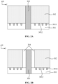
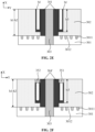
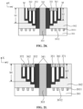
- FIGS. 2A to 2L are views showing the method of forming a heat dissipation structure according to the embodiments of the present application. The method for forming the heat dissipation structure according to the embodiments of the present application is further described in detail with reference to FIGS. 2A to 2L .
- the S101 may be executed with reference to FIG. 2A .
- a chip is provided.
- the chip comprises at least a TSV passing through a silicon substrate and a dielectric layer.
- the chip at least comprises a TSV 303 passing through a silicon substrate 301 and a dielectric layer 302.
- the dielectric layer 302 is located on a surface of the silicon substrate 301.
- the silicon substrate 301 comprises a plurality of Active Areas (AAs) 3012 isolated from each other by Shallow Trench Isolations (STI) 3011.
- AAs Active Areas
- STI Shallow Trench Isolations
- the TSV 303 may be formed by the following operations.
- a silicon substrate and a dielectric layer located on an upper surface of the substrate are provided.
- the dielectric layer and the silicon substrate are etched to form a blind hole structure in the silicon substrate, and a buffer layer, a barrier layer, and a conductive pillar are sequentially formed in the blind hole structure.
- a bottom of the silicon substrate is thinned so that the blind hole structure passes through the substrate to form the TSV.
- a top metal contact layer is formed at a top of the conductive pillar, and a bottom metal contact layer is formed at a bottom of the conductive pillar.
- the buffer layer may be, for example, SiO2, which is configured to protect the silicon substrate from being damaged.
- a material of the barrier layer may be metal tantalum, tantalum nitride, or titanium nitride, etc.
- the barrier layer is configured to prevent diffusion of the metal material of the conductive pillar subsequently filled in the TSV.
- the metal material of the conductive pillar can be any kind of conductive metal, for example, tungsten (W), cobalt (Co), copper (Cu) , aluminum (Al), etc., such as copper metal.
- a copper conductive pillar may be obtained by depositing a copper seed crystal layer by Physical Vapor Deposition (PVD) and then electroplating copper.
- PVD Physical Vapor Deposition
- a first heat dissipation ring of the heat dissipation structure is formed around the TSV in the dielectric layer.
- the S102 can be realized through the following operations.
- the dielectric layer around the TSV is etched to form a first etched annulus.
- a first etched annulus 304 is formed around the TSV 303, and the first etched annulus 304 is in contact with the TSV 303.
- the first etched annulus 304 runs through the dielectric layer 302 and is located above a surface of the AA 3012 in the silicon substrate 301.
- the dielectric layer 302 around the TSV 303 may be etched by means of a dry etching process or a wet etching process to form the first etched annulus 304.
- the dry etching process may be a plasma etching process, a reactive ion etching process or an ion milling process.
- the buffer layer, the barrier layer, and the conductive layer in the TSV are retained.
- the buffer layer in the TSV in the dielectric layer may also be removed, the buffer layer and the conductive pillar located in the TSV in the dielectric layer are retained, and the buffer layer, the barrier layer, and the conductive pillar in the TSV located in the silicon substrate are retained.
- the first heat dissipation ring of the heat dissipation structure is formed by filling the first heat conduction metal material in the first etched annulus through spin-coating.
- the first heat conduction metal material may be filled by Chemical Vapor Deposition (CVD), PVD, Atomic Layer Deposition (ALD), or any suitable deposition process.
- the first heat conduction metal material may be W, Co, Cu, Al, gold (Au) or tantalum (Ta).
- the first etched annulus 304 is filled, for example by spin- coating, with the first heat conduction metal material to form the first heat dissipation ring 341.
- the dimension h2 of the first heat dissipation ring 341 in the X-axis direction i.e. height of the first heat dissipation ring
- the first heat dissipation ring 341 surrounds the TSV 303 on the dielectric layer 302, so as to guarantee the heat dissipation effect by means of the heat conduction metal with good compactness and uniformity, and allow a good heat dissipation uniform.
- the dimension of the first heat dissipation ring 341 in the Y-axis direction i.e. width of the first heat dissipation ring
- the dimension of the first heat dissipation ring 341 in the Y-axis direction may be 0.1 ⁇ m to 2 ⁇ m, for example, 1.5 ⁇ m.
- the S103 may be executed, with reference to FIGS. 2A to 2L .
- a second heat dissipation ring of the heat dissipation structure is formed around the first heat dissipation ring.
- the S103 can be implemented through the following operations.
- the dielectric layer around the first heat dissipation ring is etched to form a second etched annulus.
- a second etched annulus 305 is formed around the first heat dissipation ring 341 by etching the dielectric layer, and the second etched annulus 305 is in contact with the first heat dissipation ring 341.
- the dimension h3 of the second etched annulus 305 in the X-axis direction is less than the dimension h2 of the first heat dissipation ring 341 in the X-axis direction, so that a dimension of the subsequently formed second heat dissipation ring in the X-axis direction is less than that of the first heat dissipation ring 341, which ensures that the outermost layer of heat dissipation ring has a relatively small area and has a good heat dissipation effect.
- the first heat dissipation ring and the second heat dissipation ring form a step-shape. This is conducive to upwards dissipating heat, avoiding the influence on bottom elements around the TSV, and also reducing the impact of stress.
- the dimension of the subsequently formed second heat dissipation ring in the X-axis direction is reduced by about 10%-20%, such as 18%, compared to this dimension of the first heat dissipation ring.
- a second heat conduction metal material of a predetermined volume is deposited, by a predetermined deposition process, on a sidewall and bottom of the second etched annulus.
- the predetermined deposition process may be CVD, PVD, ALD or any suitable deposition process.
- the second heat conduction metal material may be tungsten, cobalt, copper, aluminum, gold or tantalum.
- the predetermined volume is less than the total volume of the second etched annulus.
- the predetermined volume is greater than or equal to 10% of the total volume of the second etched annulus, and is less than or equal to 70% of the total volume of the second etched annulus.
- the heat conduction metal material of the predetermined volume is deposited on the bottom and sidewall of the second etched annulus to form a hollowed metal ring, which is conductive to heat dissipation and also reduces the manufacturing cost of the heat dissipation structure.
- a second heat conduction metal material M having a volume of 10%-70% of the total volume of the second etched annulus is deposited on the sidewall and bottom of the second etched annulus 305.
- a closure is formed at the top of the second etched annulus in which the second heat conduction metal material is deposited, so as to form the second heat dissipation ring of the heat dissipation structure.
- the formation of a closure at the top of the second etched annulus in which the second heat conduction metal material is deposited may comprise the following operations.
- a closure material is deposited by CVD process at the top of the second etched annulus in which the second heat conduction metal material is deposited, so as to form the closure.
- the closure is configured to close the top of the second etched annulus, and the closure material comprises any kind of insulation material, for example, SiO 2 .
- a closure material is deposited at the top of the second etched annulus 305 in which the second heat conduction metal material is deposited, so as to form a closure 351, and then the second heat dissipation ring 352 is formed.
- a dimension h3 of the second heat dissipation ring 352 in the X-axis direction is less than the dimension h2 of the first heat dissipation ring 341 in the X-axis direction.
- the dielectric substance may be air.
- the heat conduction metal materials are filled in the first heat dissipation ring and the second heat dissipation ring, the heat generated by the TSV can be conducted through the heat conduction metal materials.
- the hollowed structure formed between the heat conduction metals has a relatively large specific surface area, which is conductive to heat dissipation.
- the dimension of the second heat dissipation ring in the first direction is less than the dimension of the first heat dissipation ring in the first direction, a step-shaped heat dissipation structure can be formed, which can effectively reduce the occupancy of the area of the AA, reduce the stress impact and temperature impact on devices around the TSV, and improve the heat dissipation efficiency.
- the first heat conduction metal material in the first heat dissipation ring is the same as or different from the second heat conduction metal material in the second heat dissipation ring.
- the heat dissipation structure comprises at least two second heat dissipation rings.
- the heat dissipation structure comprising three second heat dissipation rings is taken as an example for description.
- FIGS. 2D to 2F illustrate a process of forming one second heat dissipation ring (that is, the first one of second heat dissipation rings), and the second etched annulus 305 is the second one of the etched annuluses of the embodiments of the present application.
- the second heat dissipation ring 352 is the second one of the second heat dissipation rings in the embodiments of the present application.
- the process of forming the second one of the second heat dissipation rings comprises the following operations.
- the dielectric layer around the first one of the second heat dissipation rings is etched to form the second one of second etched annuluses.
- the second one 306 of second etched annuluses is formed by etching the dielectric layer around the first one 352 of second heat dissipation rings, and the second one 306 of second etched annuluses is in contact with the first one 352 of second heat dissipation rings.
- a dimension h4 of the second one 306 of second etched annuluses in the X-axis direction is less than the dimension h3 of the first one 352 of second heat dissipation rings in the X-axis direction.
- a step is formed between the second one of second heat dissipation rings and the first one of second heat dissipation rings, which is conductive to upwards dissipating heat, avoiding the influence on bottom elements around the TSV, and also reducing the impact of stress.
- the dimension of the second one of second heat dissipation rings in the X-axis direction is reduced by about 10%-20%, such as 11%, compared to the dimension of the first one of second heat dissipation rings.
- a second heat conduction metal material of a predetermined volume is deposited, by the predetermined deposition process, on a sidewall and bottom of the second one of second etched annuluses.
- a second heat conduction metal material M having a volume of 10%-70% of the total volume of second one of the second etched annuluses is deposited on the sidewall and bottom of the second one 306 of second etched annuluses.
- a closure is formed at the top of the second one of second etched annuluses in which the second heat conduction metal material is deposited, so as to form the second one of second heat dissipation rings of the heat dissipation structure.
- the process of forming the closure at the top of the second one of second etched annuluses is the same as the process of forming the closure at the top of the first one of second etched annuluses in the above embodiment, and descriptions thereof will not be repeated here.
- a closure material is deposited at the top of the second one 306 of second etched annuluses in which the second heat conduction metal material M is deposited, so as to form a closure 361, and then the second one 362 of second heat dissipation rings is formed.
- a dimension h4 of the second one 362 of second heat dissipation rings in the X-axis direction is less than the dimension h3 of the first one 352 of second heat dissipation rings in the X-axis direction.
- a step is formed between the third one of the second heat dissipation rings and the second one of second heat dissipation rings, which is conductive to upwards dissipating heat, avoiding the influence on bottom elements around the TSV, and also reducing the impact of stress.
- the dimension of the third one of the heat dissipation rings in the X-axis direction is reduced by about 10%-20%, such as 15%, compared to the dimension of the second one of second heat dissipation rings.
- a process of forming the third one of the second heat dissipation rings in the embodiments of the present application can be described with reference to FIGS. 2J to 2L .
- the process of forming the third one of the second heat dissipation rings comprises the following operations.
- the dielectric layer around the second one of second heat dissipation rings is etched to form a third one of the second etched annuluses.
- the process of forming the third one of the second etched annuluses is the same as the process of forming the first one of second etched annuluses in the above embodiment, and descriptions thereof will not be repeated here.
- a third one of the second etched annuluses 307 is formed by etching the dielectric layer around the second one 362 of the second heat dissipation rings, and the third one 307 of the second etched annuluses is in contact with the second one 362 of the second heat dissipation rings.
- a dimension h5 of the third one 307 of the second etched annuluses in the X-axis direction is less than the dimension h4 of the second one 362 of second heat dissipation rings in the X-axis direction.
- a second heat conduction metal material of a predetermined volume is deposited, by the predetermined deposition process, on a sidewall and bottom of the third one of the second etched annuluses.
- the process of depositing the second heat conduction metal material in the third one of the second etched annuluses is the same as the process of depositing the second heat conduction metal material in the first one of second etched annuluses, and descriptions thereof will not be repeated here.
- a second heat conduction metal material M having a volume of 10%-70% of the total volume of the third one 307 of the second etched annuluses is deposited on the sidewall and bottom of the third one 307.
- a closure is formed at the top of the third one of the second etched annuluses in which the second heat conduction metal material is deposited, so as to form the third one of the second heat dissipation rings of the heat dissipation structure.
- the process of forming the closure at the top of the third one of the second etched annuluses is the same as the process of forming the closure at the top of the first one of second etched annuluses in the above embodiment, and descriptions thereof will not be repeated here.
- a closure material is deposited at the top of the third one 307 of the second etched annuluses in which the second heat conduction metal material M is deposited, so as to form a closure 371, and then the third one 372 of the second heat dissipation rings is formed.
- a dimension h5 of the third one 372 of the second heat dissipation rings in the X-axis direction is less than the dimension h4 of the second one 362 of second heat dissipation rings in the X-axis direction.
- the second heat conduction metal material may be tungsten, cobalt, copper, or aluminum.
- the second heat conduction metal materials filled in the first one of second etched annuluses, the second one of second etched annuluses, and the third one of the second etched annuluses may be the same or different.
- the embodiments of the present application exemplarily illustrate three second etched annuluses.
- the number of the second etched annuluses is not limited to this.
- the dimension of the third one of the second heat dissipation rings in the first direction is less than the dimension of the second one of the second heat dissipation rings in the first direction
- the dimension of the second one of second heat dissipation rings in the first direction is less than the dimension of the first one of second heat dissipation rings in the first direction
- the dimension of the first one of second heat dissipation rings in the first direction is less than the dimension of the first heat dissipation ring in the first direction.
- the formed heat dissipation structure is step-shaped, which can effectively reduce the occupancy of the area of the AA, reduce the stress impact and temperature impact on the devices around the TSV, and effectively improve the heat dissipation efficiency.
- the embodiments of the present application provide a hollowed TSV heat dissipation structure.
- Heat conduction metal particles are deposited around the TSV, and hollowed metal rings connected to one another are formed by depositing heat conduction metals for multiple times, so that the problem of difficult heat dissipation of the TSV can be effectively solved.
- Heat generated by the TSV is conducted through metals.
- the hollowed structures formed between the metals have relatively large specific surface areas, which is conductive to heat dissipation.
- the signal distortion and leakage current caused by the MOS capacitor of the TSV can be alleviated, and the static power consumption of the chip can be reduced.
- FIG. 3 is one optional schematic view of a heat dissipation structure according to the embodiments of the present application.
- the heat dissipation structure comprises a first heat dissipation ring 401 and a second heat dissipation ring 402.
- the first heat dissipation ring 401 is formed in a dielectric layer 404 around a TSV 403.
- the first heat dissipation ring 401 is in contact with the TSV 403.
- the TSV 403 passes through the silicon substrate 405 of the chip and the dielectric layer 404 located on a surface of the silicon substrate.
- the second heat dissipation ring 402 is formed around the first heat dissipation ring 401.
- the second heat dissipation ring 402 is in contact with the first heat dissipation ring 401.
- the interior of the second heat dissipation ring 402 has a heat dissipation gap 4021.
- a dimension of the second heat dissipation ring in a first direction is less than a dimension of the first heat dissipation ring in the first direction.
- the first direction is a thickness direction of the silicon substrate.
- the first direction is defined as an X-axis direction
- a second direction is defined as a Y-axis direction perpendicular to the first direction
- a first heat conduction metal material is filled in the first heat dissipation ring.
- a second heat conduction metal material of a predetermined volume is filled in the second heat dissipation ring.
- the first heat conduction metal material is the same as or different from and the second heat conduction metal material.
- the second heat conduction metal material is deposited on a bottom and sidewall of the second heat dissipation ring.
- the predetermined volume is less than the total volume of the second heat dissipation ring.
- the predetermined volume is greater than or equal to 10% of the total volume of the second heat dissipation ring.
- the predetermined volume is less than or equal to 70% of the total volume of the second heat dissipation ring.
- the dimension of the second heat dissipation ring in the second direction is 0.1 ⁇ m to 1 ⁇ m.
- the second direction is perpendicular to the first direction.
- the heat conduction metal materials are filled in the first heat dissipation ring and the first one of second heat dissipation rings, the heat generated by the TSV can be conducted through the heat conduction metals.
- the hollowed structure formed between the heat conduction metals has a relatively large specific surface area, which is conductive to heat dissipation.
- the dimension of the second heat dissipation ring in the first direction is less than the dimension of the first heat dissipation ring in the first direction, a step-shaped heat dissipation structure can be formed, which can effectively reduce the occupancy of the area of an AA, reduce the stress impact and temperature impact on devices around the TSV, and improve the heat dissipation efficiency.
- the heat dissipation structure comprises at least two second heat dissipation rings, and any two adjacent second heat dissipation rings are in contact with each other. Dimensions in the X axis, of the at least two second heat dissipation rings arranged successively in a direction from center of the TSV to the outside, sequentially decrease.
- the dimensions of any two second heat dissipation rings in the second direction are the same or different.
- the dimension of the first one of second heat dissipation rings in the Y-axis direction may be 0.5 ⁇ m
- the dimension of the second one of second heat dissipation rings in the Y-axis direction may be 0.5 ⁇ m
- the dimension of the second one of second heat dissipation rings in the Y-axis direction may also be 0.8 ⁇ m.
- a first dimension difference in the first direction between the first heat dissipation ring and the second heat dissipation ring adjacent to it is different from or the same as a second dimension difference in the first direction between any two adjacent second heat dissipation rings.
- Any two adjacent second heat dissipation rings may have the same dimension or different dimensions in the first direction.
- the method for forming the heat dissipation structure in the embodiment of the present application is similar to the method for forming the heat dissipation structure in the above embodiments.
- Technical features that are not disclosed in detail in the embodiments of the present application can be understood with reference to the foregoing embodiments. Descriptions thereof are omitted here.
- the heat dissipation structure Due to the hollowed metal rings of the heat dissipation structure, the heat dissipation structure according to the embodiments of the present application can effectively solve the heat dissipation problem of the TSV.
- the heat generated by the TSV is conducted through the heat conduction metals.
- the hollowed structures formed between the heat conduction metals have relatively large specific surface areas, which is conductive to heat dissipation.
- the signal distortion and leakage current caused by the MOS capacitor of the TSV can be alleviated, and the static power consumption of the chip can be reduced.
- FIG. 4 is one optional schematic view of a semiconductor structure according to the embodiments of the present application.
- the semiconductor structure 60 comprises a TSV 601 and a heat dissipation structure 602.
- the TSV 601 passes through the silicon substrate 603 and a dielectric layer 604 located on a surface of the silicon substrate.
- the heat dissipation structure 602 is formed in the dielectric layer around the TSV 601, and the heat dissipation structure 602 is in contact with the TSV 601.
- the heat dissipation structure is configured to dissipate heat generated by the TSV.
- the heat dissipation structure comprises a first heat dissipation ring 6021 and at least one second heat dissipation ring 6022.
- the first heat dissipation ring is in contact with the TSV.
- the second heat dissipation ring is in contact with the first heat dissipation ring, and has a heat dissipation gap in the interior of the second heat dissipation ring.
- a dimension of the second heat dissipation ring in the first direction is less than that of the first heat dissipation ring in the first direction.
- the first direction is a thickness direction of the silicon substrate.
- any two adjacent second heat dissipation rings are in contact with each other.
- Dimensions, in the first direction, of the at least two second heat dissipation rings extending to the outside along the center of the TSV sequentially decrease.
- the heat dissipation structure in the semiconductor structure according to the embodiments of the present application is similar to the heat dissipation structure or the method for forming the heat dissipation structure in the foregoing embodiment.
- Technical features that are not disclosed in detail in the embodiments of the present application are understood with reference to the foregoing embodiments. Descriptions thereof are omitted here.
- the semiconductor structure according to the embodiments of the present application comprises a heat dissipation structure located on an outer side of the TSV.
- the heat generated by the TSV can be dissipated, thereby improving the electrical performance of the semiconductor structure while improving the reliability and stability of the STV.
- the device in the embodiments described above are merely illustrative. In actual implementation, there may be another manner. For example, a plurality of units or components may be combined, or integrated into another system, or some features may be ignored or not executed. In addition, all the components illustrated or discussed may be coupled or directly coupled to each other.
Landscapes
- Internal Circuitry In Semiconductor Integrated Circuit Devices (AREA)
Abstract
Description
- The present application is based upon and claims priority to
Chinese Patent Application No. 202110766667.2, filed on July 7, 2021 - The embodiments of the present application relate to, but are not limited to, a heat dissipation structure, a method for forming a heat dissipation structure, and a semiconductor structure.
- Due to the continuous improvement of chip integration, the number of device units on each chip has increased sharply, resulting in a continuous increase in an area of a chip. However, various electronic devices have higher requirements for the area, volume, power consumption, cost, and performance of the chip. Therefore, it gave rise to a three-dimensional integrated Through Silicon Via (TSV) vertical interconnection technology.
- In the related art, since a TSV stacks multiple layers of chips together, a power density rises sharply. Greater heat and poor heat dissipation make the operating temperature of the chip rise. However, only the first layer of chip is adjacent to a heat sink so that heat dissipation is very difficult, resulting in an excessive heat density inside the chip, which seriously affects the reliability and stability of the TSV. In addition, a metal material in the TSV will expand and contract due to a thermal stress. This phenomenon easily causes stress deformation of a silicon substrate and a dielectric layer, which in turn affects the characteristics of elements in an Active Area (AA).
- In addition, in the related art, one isolation dielectric layer (for example, SiO2) is generally arranged around the TSV to achieve electrical isolation from the silicon substrate. However, this will generate a Metal-Oxide-Semiconductor (MOS) capacitor. The MOS capacitor will cause a signal on the TSV to be coupled to the silicon substrate or surrounding devices and TSVs, resulting in signal distortion and leakage current, which increases the static power consumption of the chip.
- The embodiments of the present application provide a heat dissipation structure, comprising: a first heat dissipation ring and a second heat dissipation ring. The first heat dissipation ring is formed in a dielectric layer around a Through Silicon Via (TSV) and is in contact with the TSV. The TSV passes through a silicon substrate of a chip and the dielectric layer located on a surface of the silicon substrate. The second heat dissipation ring is formed around the first heat dissipation ring and is in contact with the first heat dissipation ring. The interior of the second heat dissipation ring has a heat dissipation gap. A dimension of the second heat dissipation ring in a first direction is less than a dimension of the first heat dissipation ring in the first direction. The first direction is a thickness direction of the silicon substrate.
- The embodiments of the present application further provide a method for forming a heat dissipation structure, comprising: providing a chip, the chip at least comprising a Through Silicon Via (TSV) passing through a silicon substrate and a dielectric layer; forming a first heat dissipation ring of the heat dissipation ring around the TSV in the dielectric layer in the dielectric layer, the first heat dissipation ring being in contact with the TSV; and forming a second heat dissipation ring of the heat dissipation structure around the first heat dissipation ring. The second heat dissipation ring is in contact with the first heat dissipation ring and has a heat dissipation gap in the interior thereof. A dimension of the second heat dissipation ring in a first direction is less than a dimension of the first heat dissipation ring in the first direction. The first direction is a thickness direction of the silicon substrate.
- In the drawings (not necessarily drawn according to a proportion), similar reference signs can describe similar parts in the different diagrams. Similar reference signs with different letter suffixes can represent different examples of the similar parts. The drawings almost show every embodiment discussed herein with examples rather than in a limiting manner.
-
FIG. 1 is a flow chart of a method for forming a heat dissipation structure according to the embodiments of the present application; -
FIGS. 2A-2L are views of a method for forming a heat dissipation structure according to the embodiments of the present application; -
FIG. 3 is a schematic view of a heat dissipation structure according to the embodiments of the present application; and -
FIG. 4 is a schematic view of a semiconductor structure according to the embodiments of the present application. - The specific technical solutions of the invention will be further described in detail below in combination with accompanying drawings in the embodiments of the present application. The embodiments below are used to illustrate the present application, but are not intended to limit the scope of the present application.
- Based on the problems in the related art, the embodiments of the present application provide a method for forming a heat dissipation structure. Heat conduction metal particles are deposited around a Through Silicon Via (TSV), and hollowed metal rings connected to one another are formed by depositing the heat conduction metal for multiple times. Heat generated by the TSV can be dissipated by the high heat conductivity of metal, thus effectively solving the problem of difficult heat dissipation of the TSV. In the embodiments of the present application, the heat generated by the TSV is conducted by metals. The hollowed structures formed between the metals have a relatively large specific surface area, which is favorable for heat dissipation. Spaces between the hollowed metals are full of air that has an extremely low dielectric constant, so that signal distortion and leakage current caused by a Metal-Oxide-Semiconductor (MOS) capacitor of the TSV can be alleviated and the static power consumption of a chip can be reduced. In addition, the heat dissipation structure formed by the embodiments of the present application is a heat dissipation ring of a step-shaped structure, which is not only favorable for upwards dissipating heat, but also can effectively reduce the occupancy of the area of an Active Area (AA), so as to avoid stress impact and temperature impact on devices around the TSV and effectively improve the heat dissipation efficiency.
-
FIG. 1 is flow chart of a method for forming a heat dissipation structure according to the embodiments of the present application. As shown inFIG. 1 , the method comprises the following operations. - At S101, a chip is provided. The chip at least comprises a TSV passing through a silicon substrate and a dielectric layer.
- Various active devices and circuits are formed inside the chip to realize a variety of functions. In the embodiments of the present application, the chip at least comprises the silicon substrate.
- The TSV is a via formed inside the chip and passes through the silicon substrate of the chip. The TSV is filled with a conductive material to transmit a signal from a front surface of the chip to a back surface of the chip.
- The silicon substrate may comprise a top surface located on the front face and a bottom surface located on the back face opposite to the front face. If the flatness of the top surface and the bottom surface of the silicon substrate is disregarded, a direction perpendicular to the top surface and the bottom surface of the silicon substrate is defined as a first direction, i.e., a thickness direction of the silicon substrate. In the top surface and the bottom surface of the silicon substrate (i.e., a plane where the silicon substrate is located), any direction is defined as a second direction. The first direction is perpendicular to the second direction. In the embodiments of the present application, the first direction is defined as an X-axis direction and the second direction is defined as a Y-axis direction.
- The dielectric layer is formed on a surface of the silicon substrate and is configured for protecting the silicon substrate. In the embodiments of the present application, the dielectric layer may be a SiO2 layer or other insulation material layer.
- At S102, a first heat dissipation ring of the heat dissipation structure is formed around the TSV in the dielectric layer.
- The first heat dissipation ring is in contact with the TSV.
- In the embodiments of the present application, the first heat dissipation ring may pass through the dielectric layer, or may not pass through the dielectric layer. That is, a dimension of the first heat dissipation ring in the first direction is less than or equal to that of the dielectric layer in the first direction. The first heat dissipation ring is filled with a heat conduction metal material. Heat generated by the TSV is dissipated by the high heat conductivity of the metal material.
- At S103, a second heat dissipation ring of the heat dissipation structure is formed around the first heat dissipation ring.
- The second heat dissipation ring is in contact with the first heat dissipation ring and has a heat dissipation gap within the second heat dissipation. A dimension of the second heat dissipation ring in the first direction is less than that of the first heat dissipation ring in the first direction. The first direction is the thickness direction of the silicon substrate.
- In the embodiments of the present application, since the dimension of the second heat dissipation ring in the first direction is less than that of the first heat dissipation ring in the first direction, the first heat dissipation ring and the second heat dissipation ring form a step-shaped heat dissipation structure.
- It should be noted that in the embodiments of the present application, there may be one second heat dissipation ring, or may be at least two second heat dissipation rings. When the heat dissipation structure comprises at least two heat dissipation rings, any two adjacent second heat dissipation rings are in contact with each other. The dimensions in the first direction, of the at least two second heat dissipation rings extending towards the outside along the center of the TSV, sequentially decrease.
- In the embodiments of the present application, since the TSV is formed in a keep-out-zone (KOZ) of the silicon substrate, the heat dissipation structure is also formed in the KOZ of the silicon substrate.
- In the method for forming the heat dissipation structure according to the embodiments of the present application, since the heat dissipation structure comprising the first heat dissipation ring and the second heat dissipation ring is formed at a periphery of the TSV, the heat generated by the TSV can be dissipated to the outside of the chip, thereby improving the reliability and stability of the TSV.
-
FIGS. 2A to 2L are views showing the method of forming a heat dissipation structure according to the embodiments of the present application. The method for forming the heat dissipation structure according to the embodiments of the present application is further described in detail with reference toFIGS. 2A to 2L . - First, the S101 may be executed with reference to
FIG. 2A . A chip is provided. The chip comprises at least a TSV passing through a silicon substrate and a dielectric layer. - As shown in
FIG. 2A , the chip at least comprises aTSV 303 passing through asilicon substrate 301 and adielectric layer 302. Thedielectric layer 302 is located on a surface of thesilicon substrate 301. Thesilicon substrate 301 comprises a plurality of Active Areas (AAs) 3012 isolated from each other by Shallow Trench Isolations (STI) 3011. - In some embodiments, the
TSV 303 may be formed by the following operations. - A silicon substrate and a dielectric layer located on an upper surface of the substrate are provided.
- The dielectric layer and the silicon substrate are etched to form a blind hole structure in the silicon substrate, and a buffer layer, a barrier layer, and a conductive pillar are sequentially formed in the blind hole structure.
- A bottom of the silicon substrate is thinned so that the blind hole structure passes through the substrate to form the TSV. A top metal contact layer is formed at a top of the conductive pillar, and a bottom metal contact layer is formed at a bottom of the conductive pillar.
- In some embodiments, the buffer layer may be, for example, SiO2, which is configured to protect the silicon substrate from being damaged. A material of the barrier layer may be metal tantalum, tantalum nitride, or titanium nitride, etc. The barrier layer is configured to prevent diffusion of the metal material of the conductive pillar subsequently filled in the TSV. The metal material of the conductive pillar can be any kind of conductive metal, for example, tungsten (W), cobalt (Co), copper (Cu) , aluminum (Al), etc., such as copper metal. Specifically, a copper conductive pillar may be obtained by depositing a copper seed crystal layer by Physical Vapor Deposition (PVD) and then electroplating copper. The TSV provides a conductive effect by means of a top metal contact layer and a bottom metal contact layer in the conductive pillar.
- Next, the S102 may be executed, with reference to
FIGS. 2B and2C . A first heat dissipation ring of the heat dissipation structure is formed around the TSV in the dielectric layer. - In some embodiments, the S102 can be realized through the following operations.
- The dielectric layer around the TSV is etched to form a first etched annulus.
- As shown in
FIG. 2B , a firstetched annulus 304 is formed around theTSV 303, and the firstetched annulus 304 is in contact with theTSV 303. In the embodiments of the present application, the firstetched annulus 304 runs through thedielectric layer 302 and is located above a surface of theAA 3012 in thesilicon substrate 301. - In the embodiments of the present application, the
dielectric layer 302 around theTSV 303 may be etched by means of a dry etching process or a wet etching process to form the firstetched annulus 304. The dry etching process may be a plasma etching process, a reactive ion etching process or an ion milling process. - In the embodiments of the present application, when the dielectric layer around the TSV is etched to form the first etched annulus, the buffer layer, the barrier layer, and the conductive layer in the TSV are retained.
- In other embodiments, when the dielectric layer around the TSV is etched to form the first etched annulus, the buffer layer in the TSV in the dielectric layer may also be removed, the buffer layer and the conductive pillar located in the TSV in the dielectric layer are retained, and the buffer layer, the barrier layer, and the conductive pillar in the TSV located in the silicon substrate are retained.
- In the embodiments of the present application, the first heat dissipation ring of the heat dissipation structure is formed by filling the first heat conduction metal material in the first etched annulus through spin-coating.
- In other embodiments, the first heat conduction metal material may be filled by Chemical Vapor Deposition (CVD), PVD, Atomic Layer Deposition (ALD), or any suitable deposition process. The first heat conduction metal material may be W, Co, Cu, Al, gold (Au) or tantalum (Ta).
- As shown in
FIG. 2C , the firstetched annulus 304 is filled, for example by spin- coating, with the first heat conduction metal material to form the firstheat dissipation ring 341. The dimension h2 of the firstheat dissipation ring 341 in the X-axis direction (i.e. height of the first heat dissipation ring) is equal to the dimension h1 of the dielectric layer in the X-axis direction. At this time, the firstheat dissipation ring 341 surrounds theTSV 303 on thedielectric layer 302, so as to guarantee the heat dissipation effect by means of the heat conduction metal with good compactness and uniformity, and allow a good heat dissipation uniform. In addition, for ensuring the heat dissipation effect, the dimension of the firstheat dissipation ring 341 in the Y-axis direction (i.e. width of the first heat dissipation ring) may be 0.1 µm to 2 µm, for example, 1.5 µm. - Next, the S103 may be executed, with reference to
FIGS. 2A to 2L . A second heat dissipation ring of the heat dissipation structure is formed around the first heat dissipation ring. - In some embodiments, the S103 can be implemented through the following operations.
- The dielectric layer around the first heat dissipation ring is etched to form a second etched annulus.
- As shown in
FIG. 2D , a secondetched annulus 305 is formed around the firstheat dissipation ring 341 by etching the dielectric layer, and the secondetched annulus 305 is in contact with the firstheat dissipation ring 341. The dimension h3 of the secondetched annulus 305 in the X-axis direction is less than the dimension h2 of the firstheat dissipation ring 341 in the X-axis direction, so that a dimension of the subsequently formed second heat dissipation ring in the X-axis direction is less than that of the firstheat dissipation ring 341, which ensures that the outermost layer of heat dissipation ring has a relatively small area and has a good heat dissipation effect. The first heat dissipation ring and the second heat dissipation ring form a step-shape. This is conducive to upwards dissipating heat, avoiding the influence on bottom elements around the TSV, and also reducing the impact of stress. - In some embodiments, the dimension of the subsequently formed second heat dissipation ring in the X-axis direction is reduced by about 10%-20%, such as 18%, compared to this dimension of the first heat dissipation ring.
- A second heat conduction metal material of a predetermined volume is deposited, by a predetermined deposition process, on a sidewall and bottom of the second etched annulus.
- In the embodiments of the present application, the predetermined deposition process may be CVD, PVD, ALD or any suitable deposition process. The second heat conduction metal material may be tungsten, cobalt, copper, aluminum, gold or tantalum. The predetermined volume is less than the total volume of the second etched annulus. The predetermined volume is greater than or equal to 10% of the total volume of the second etched annulus, and is less than or equal to 70% of the total volume of the second etched annulus. In the embodiments of the present application, the heat conduction metal material of the predetermined volume is deposited on the bottom and sidewall of the second etched annulus to form a hollowed metal ring, which is conductive to heat dissipation and also reduces the manufacturing cost of the heat dissipation structure. As shown in
FIG. 2E , a second heat conduction metal material M having a volume of 10%-70% of the total volume of the second etched annulus is deposited on the sidewall and bottom of the secondetched annulus 305. - A closure is formed at the top of the second etched annulus in which the second heat conduction metal material is deposited, so as to form the second heat dissipation ring of the heat dissipation structure.
- In some embodiments, the formation of a closure at the top of the second etched annulus in which the second heat conduction metal material is deposited may comprise the following operations.
- A closure material is deposited by CVD process at the top of the second etched annulus in which the second heat conduction metal material is deposited, so as to form the closure.
- In the embodiments of the present application, the closure is configured to close the top of the second etched annulus, and the closure material comprises any kind of insulation material, for example, SiO2.
- As shown in
FIG. 2F , a closure material is deposited at the top of the secondetched annulus 305 in which the second heat conduction metal material is deposited, so as to form aclosure 351, and then the secondheat dissipation ring 352 is formed. A dimension h3 of the secondheat dissipation ring 352 in the X-axis direction is less than the dimension h2 of the firstheat dissipation ring 341 in the X-axis direction. - In the embodiments of the present application, since only the second heat conduction metal material of the predetermined volume is deposited in the second etched annulus, and the predetermined volume is less than the total volume of the second etched annulus, a gap is formed inside the second etched annulus, which is conductive to heat dissipation. In addition, there is a dielectric substance having a relatively low dielectric constant in the gap, which can improve the MOS capacitor problem caused by the TSV. In some embodiments, the dielectric substance may be air.
- In the embodiments of the present application, since the heat conduction metal materials are filled in the first heat dissipation ring and the second heat dissipation ring, the heat generated by the TSV can be conducted through the heat conduction metal materials. The hollowed structure formed between the heat conduction metals has a relatively large specific surface area, which is conductive to heat dissipation. In addition, since the dimension of the second heat dissipation ring in the first direction is less than the dimension of the first heat dissipation ring in the first direction, a step-shaped heat dissipation structure can be formed, which can effectively reduce the occupancy of the area of the AA, reduce the stress impact and temperature impact on devices around the TSV, and improve the heat dissipation efficiency.
- In some embodiments, the first heat conduction metal material in the first heat dissipation ring is the same as or different from the second heat conduction metal material in the second heat dissipation ring.
- In some embodiments, the heat dissipation structure comprises at least two second heat dissipation rings. In the embodiments of the present application, the heat dissipation structure comprising three second heat dissipation rings is taken as an example for description.
- It should be note that the foregoing
FIGS. 2D to 2F illustrate a process of forming one second heat dissipation ring (that is, the first one of second heat dissipation rings), and the secondetched annulus 305 is the second one of the etched annuluses of the embodiments of the present application. The secondheat dissipation ring 352 is the second one of the second heat dissipation rings in the embodiments of the present application. - Next, a process of forming the second one of the second heat dissipation rings in the embodiments of the present application will be described with reference to
FIGS. 2G to 2I . The process of forming the second one of the second heat dissipation rings comprises the following operations. - The dielectric layer around the first one of the second heat dissipation rings is etched to form the second one of second etched annuluses.
- As shown in
FIG. 2G , the second one 306 of second etched annuluses is formed by etching the dielectric layer around the first one 352 of second heat dissipation rings, and the second one 306 of second etched annuluses is in contact with the first one 352 of second heat dissipation rings. A dimension h4 of the second one 306 of second etched annuluses in the X-axis direction is less than the dimension h3 of the first one 352 of second heat dissipation rings in the X-axis direction. In the embodiments of the present application, a step is formed between the second one of second heat dissipation rings and the first one of second heat dissipation rings, which is conductive to upwards dissipating heat, avoiding the influence on bottom elements around the TSV, and also reducing the impact of stress. - In some embodiments, the dimension of the second one of second heat dissipation rings in the X-axis direction is reduced by about 10%-20%, such as 11%, compared to the dimension of the first one of second heat dissipation rings.
- A second heat conduction metal material of a predetermined volume is deposited, by the predetermined deposition process, on a sidewall and bottom of the second one of second etched annuluses.
- As shown in
FIG. 2H , a second heat conduction metal material M having a volume of 10%-70% of the total volume of second one of the second etched annuluses is deposited on the sidewall and bottom of the second one 306 of second etched annuluses. - In the embodiments of the present application, since only the second heat conduction metal material of the predetermined volume is deposited in the second one of second etched annuluses, and the predetermined volume is less than the total volume of the second one of the second etched annuluses, a gap is formed inside the second one of second etched annuluses, which is conductive to heat dissipation.
- A closure is formed at the top of the second one of second etched annuluses in which the second heat conduction metal material is deposited, so as to form the second one of second heat dissipation rings of the heat dissipation structure.
- In the embodiments of the present application, the process of forming the closure at the top of the second one of second etched annuluses is the same as the process of forming the closure at the top of the first one of second etched annuluses in the above embodiment, and descriptions thereof will not be repeated here.
- As shown in
FIG. 2I , a closure material is deposited at the top of the second one 306 of second etched annuluses in which the second heat conduction metal material M is deposited, so as to form aclosure 361, and then the second one 362 of second heat dissipation rings is formed. A dimension h4 of the second one 362 of second heat dissipation rings in the X-axis direction is less than the dimension h3 of the first one 352 of second heat dissipation rings in the X-axis direction. In the embodiments of the present application, a step is formed between the third one of the second heat dissipation rings and the second one of second heat dissipation rings, which is conductive to upwards dissipating heat, avoiding the influence on bottom elements around the TSV, and also reducing the impact of stress. - In some embodiments, the dimension of the third one of the heat dissipation rings in the X-axis direction is reduced by about 10%-20%, such as 15%, compared to the dimension of the second one of second heat dissipation rings.
- A process of forming the third one of the second heat dissipation rings in the embodiments of the present application can be described with reference to
FIGS. 2J to 2L . The process of forming the third one of the second heat dissipation rings comprises the following operations. - The dielectric layer around the second one of second heat dissipation rings is etched to form a third one of the second etched annuluses.
- In the embodiments of the present application, the process of forming the third one of the second etched annuluses is the same as the process of forming the first one of second etched annuluses in the above embodiment, and descriptions thereof will not be repeated here.
- As shown in
FIG. 2J , a third one of the secondetched annuluses 307 is formed by etching the dielectric layer around the second one 362 of the second heat dissipation rings, and the third one 307 of the second etched annuluses is in contact with the second one 362 of the second heat dissipation rings. A dimension h5 of the third one 307 of the second etched annuluses in the X-axis direction is less than the dimension h4 of the second one 362 of second heat dissipation rings in the X-axis direction. - A second heat conduction metal material of a predetermined volume is deposited, by the predetermined deposition process, on a sidewall and bottom of the third one of the second etched annuluses.
- In the embodiments of the present application, the process of depositing the second heat conduction metal material in the third one of the second etched annuluses is the same as the process of depositing the second heat conduction metal material in the first one of second etched annuluses, and descriptions thereof will not be repeated here.
- As shown in
FIG. 2K , a second heat conduction metal material M having a volume of 10%-70% of the total volume of the third one 307 of the second etched annuluses is deposited on the sidewall and bottom of thethird one 307. - In the embodiments of the present application, since only the second heat conduction metal material of the predetermined volume is deposited in the third one of the second etched annuluses, and the predetermined volume is less than the total volume of the third one of second etched annuluses, a gap is formed inside the third one of second etched annuluses, which is conductive to heat dissipation.
- A closure is formed at the top of the third one of the second etched annuluses in which the second heat conduction metal material is deposited, so as to form the third one of the second heat dissipation rings of the heat dissipation structure.
- In the embodiments of the present application, the process of forming the closure at the top of the third one of the second etched annuluses is the same as the process of forming the closure at the top of the first one of second etched annuluses in the above embodiment, and descriptions thereof will not be repeated here.
- As shown in
FIG. 2L , a closure material is deposited at the top of the third one 307 of the second etched annuluses in which the second heat conduction metal material M is deposited, so as to form aclosure 371, and then the third one 372 of the second heat dissipation rings is formed. A dimension h5 of the third one 372 of the second heat dissipation rings in the X-axis direction is less than the dimension h4 of the second one 362 of second heat dissipation rings in the X-axis direction. - In the embodiments of the present application, the second heat conduction metal material may be tungsten, cobalt, copper, or aluminum. The second heat conduction metal materials filled in the first one of second etched annuluses, the second one of second etched annuluses, and the third one of the second etched annuluses may be the same or different.
- It should be noted that the embodiments of the present application exemplarily illustrate three second etched annuluses. In an actual process, the number of the second etched annuluses is not limited to this.
- In the embodiments of the present application, the dimension of the third one of the second heat dissipation rings in the first direction is less than the dimension of the second one of the second heat dissipation rings in the first direction, the dimension of the second one of second heat dissipation rings in the first direction is less than the dimension of the first one of second heat dissipation rings in the first direction, and the dimension of the first one of second heat dissipation rings in the first direction is less than the dimension of the first heat dissipation ring in the first direction. Therefore, in the embodiments of the present application, the formed heat dissipation structure is step-shaped, which can effectively reduce the occupancy of the area of the AA, reduce the stress impact and temperature impact on the devices around the TSV, and effectively improve the heat dissipation efficiency.
- The embodiments of the present application provide a hollowed TSV heat dissipation structure. Heat conduction metal particles are deposited around the TSV, and hollowed metal rings connected to one another are formed by depositing heat conduction metals for multiple times, so that the problem of difficult heat dissipation of the TSV can be effectively solved. Heat generated by the TSV is conducted through metals. The hollowed structures formed between the metals have relatively large specific surface areas, which is conductive to heat dissipation. In another aspect, since there is an air gap in the heat dissipation structure, and the air has a very low dielectric constant, the signal distortion and leakage current caused by the MOS capacitor of the TSV can be alleviated, and the static power consumption of the chip can be reduced.
- The embodiments of the present application also provide a heat dissipation structure for dissipating the heat generated by the TSV.
FIG. 3 is one optional schematic view of a heat dissipation structure according to the embodiments of the present application. As shown inFIG. 3 , the heat dissipation structure comprises a firstheat dissipation ring 401 and a secondheat dissipation ring 402. - The first
heat dissipation ring 401 is formed in adielectric layer 404 around aTSV 403. The firstheat dissipation ring 401 is in contact with theTSV 403. TheTSV 403 passes through thesilicon substrate 405 of the chip and thedielectric layer 404 located on a surface of the silicon substrate. - The second
heat dissipation ring 402 is formed around the firstheat dissipation ring 401. The secondheat dissipation ring 402 is in contact with the firstheat dissipation ring 401. The interior of the secondheat dissipation ring 402 has aheat dissipation gap 4021. A dimension of the second heat dissipation ring in a first direction is less than a dimension of the first heat dissipation ring in the first direction. The first direction is a thickness direction of the silicon substrate. - In the embodiments of the present application, the first direction is defined as an X-axis direction, and a second direction is defined as a Y-axis direction perpendicular to the first direction.
- In the embodiments of the present application, a first heat conduction metal material is filled in the first heat dissipation ring. A second heat conduction metal material of a predetermined volume is filled in the second heat dissipation ring. The first heat conduction metal material is the same as or different from and the second heat conduction metal material.
- In the embodiments of the present application, the second heat conduction metal material is deposited on a bottom and sidewall of the second heat dissipation ring. The predetermined volume is less than the total volume of the second heat dissipation ring. The predetermined volume is greater than or equal to 10% of the total volume of the second heat dissipation ring. In addition, the predetermined volume is less than or equal to 70% of the total volume of the second heat dissipation ring.
- In some embodiments, the dimension of the second heat dissipation ring in the second direction is 0.1 µm to 1 µm. The second direction is perpendicular to the first direction.
- In the embodiments of the present application, since the heat conduction metal materials are filled in the first heat dissipation ring and the first one of second heat dissipation rings, the heat generated by the TSV can be conducted through the heat conduction metals. The hollowed structure formed between the heat conduction metals has a relatively large specific surface area, which is conductive to heat dissipation. In addition, since the dimension of the second heat dissipation ring in the first direction is less than the dimension of the first heat dissipation ring in the first direction, a step-shaped heat dissipation structure can be formed, which can effectively reduce the occupancy of the area of an AA, reduce the stress impact and temperature impact on devices around the TSV, and improve the heat dissipation efficiency.
- In some embodiments, the heat dissipation structure comprises at least two second heat dissipation rings, and any two adjacent second heat dissipation rings are in contact with each other. Dimensions in the X axis, of the at least two second heat dissipation rings arranged successively in a direction from center of the TSV to the outside, sequentially decrease.
- In some embodiments, the dimensions of any two second heat dissipation rings in the second direction are the same or different. For example, when the heat dissipation structure comprises two second heat dissipation rings, the dimension of the first one of second heat dissipation rings in the Y-axis direction may be 0.5 µm, and the dimension of the second one of second heat dissipation rings in the Y-axis direction may be 0.5 µm, or the dimension of the second one of second heat dissipation rings in the Y-axis direction may also be 0.8 µm.
- In some embodiments, a first dimension difference in the first direction between the first heat dissipation ring and the second heat dissipation ring adjacent to it, is different from or the same as a second dimension difference in the first direction between any two adjacent second heat dissipation rings. Any two adjacent second heat dissipation rings may have the same dimension or different dimensions in the first direction.
- The method for forming the heat dissipation structure in the embodiment of the present application is similar to the method for forming the heat dissipation structure in the above embodiments. Technical features that are not disclosed in detail in the embodiments of the present application can be understood with reference to the foregoing embodiments. Descriptions thereof are omitted here.
- Due to the hollowed metal rings of the heat dissipation structure, the heat dissipation structure according to the embodiments of the present application can effectively solve the heat dissipation problem of the TSV. The heat generated by the TSV is conducted through the heat conduction metals. The hollowed structures formed between the heat conduction metals have relatively large specific surface areas, which is conductive to heat dissipation. In another aspect, since there is an air gap in the heat dissipation structure of the embodiments of the present application and the air has a very low dielectric constant, the signal distortion and leakage current caused by the MOS capacitor of the TSV can be alleviated, and the static power consumption of the chip can be reduced.
- In addition, the embodiments of the present application further provide a semiconductor structure.
FIG. 4 is one optional schematic view of a semiconductor structure according to the embodiments of the present application. As shown inFIG. 4 , thesemiconductor structure 60 comprises aTSV 601 and aheat dissipation structure 602. - The
TSV 601 passes through thesilicon substrate 603 and adielectric layer 604 located on a surface of the silicon substrate. - The
heat dissipation structure 602 is formed in the dielectric layer around theTSV 601, and theheat dissipation structure 602 is in contact with theTSV 601. - In the embodiments of the present application, the heat dissipation structure is configured to dissipate heat generated by the TSV.
- In some embodiments, the heat dissipation structure comprises a first
heat dissipation ring 6021 and at least one secondheat dissipation ring 6022. The first heat dissipation ring is in contact with the TSV. The second heat dissipation ring is in contact with the first heat dissipation ring, and has a heat dissipation gap in the interior of the second heat dissipation ring. A dimension of the second heat dissipation ring in the first direction is less than that of the first heat dissipation ring in the first direction. The first direction is a thickness direction of the silicon substrate. - In some embodiments, any two adjacent second heat dissipation rings are in contact with each other. Dimensions, in the first direction, of the at least two second heat dissipation rings extending to the outside along the center of the TSV sequentially decrease.
- The heat dissipation structure in the semiconductor structure according to the embodiments of the present application is similar to the heat dissipation structure or the method for forming the heat dissipation structure in the foregoing embodiment. Technical features that are not disclosed in detail in the embodiments of the present application are understood with reference to the foregoing embodiments. Descriptions thereof are omitted here.
- The semiconductor structure according to the embodiments of the present application comprises a heat dissipation structure located on an outer side of the TSV. By means of the heat dissipation structure, the heat generated by the TSV can be dissipated, thereby improving the electrical performance of the semiconductor structure while improving the reliability and stability of the STV.
- The device in the embodiments described above are merely illustrative. In actual implementation, there may be another manner. For example, a plurality of units or components may be combined, or integrated into another system, or some features may be ignored or not executed. In addition, all the components illustrated or discussed may be coupled or directly coupled to each other.
- The features disclosed in the several method or device embodiments provided in the present application can be combined arbitrarily without conflict to obtain a new method embodiment or device embodiment.
- The foregoing descriptions are merely implementation modes of the present application, but the protection scope of the present application is not limited thereto. Any person skilled in the art can easily think that changes or replacements within the technical scope disclosed in the present application shall fall within the protection scope of the present application. Therefore, the protection scope of the present application should be subject to the appended claims.
Claims (15)
- A heat dissipation structure, comprising a first heat dissipation ring and at least one second heat dissipation ring, whereinthe first heat dissipation ring is formed in a dielectric layer around a through silicon via and is in contact with the through silicon via, wherein the through silicon via passes through a silicon substrate of a chip and the dielectric layer located on a surface of the silicon substrate;the second heat dissipation ring is formed around the first heat dissipation ring and is in contact with the first heat dissipation ring, the second heat dissipation ring has a heat dissipation gap in an interior of the second heat dissipation ring, a dimension of the second heat dissipation ring in a first direction is less than a dimension of the first heat dissipation ring in the first direction, and the first direction is a thickness direction of the silicon substrate.
- The heat dissipation structure according to claim 1, wherein the heat dissipation structure comprises at least two second heat dissipation rings, and any two adjacent second heat dissipation rings are in contact with each other;
the dimensions in the first direction, of the at least two second heat dissipation rings arranged successively in a direction from an center of the through silicon via to an outside of the through silicon via, sequentially decrease. - The heat dissipation structure according to claim 2, wherein a first heat conduction metal material is filled in the first heat dissipation ring, and a second heat conduction metal material of a predetermined volume is filled in each second heat dissipation ring;
the first heat conduction metal material is the same as or different from the second heat conduction metal material. - The heat dissipation structure according to claim 3, wherein the second heat conduction metal material is deposited on a bottom and sidewall of the second heat dissipation ring;
the predetermined volume is greater than or equal to 10% of a total volume of the second heat dissipation ring; and the predetermined volume is less than or equal to 70% of the total volume of the second heat dissipation ring. - The heat dissipation structure according to any one of claims 2 to 4, wherein the dimension of the second heat dissipation ring in the second direction is 0.1 µm to 1 µm;
the dimensions in a second direction of any two second heat dissipation rings are the same or different, and the second direction is perpendicular to the first direction. - The heat dissipation structure according to any one of claims 2 to 4, wherein a first dimension difference in the first direction between the first heat dissipation ring and the second heat dissipation ring adjacent to the first heat dissipation ring, and a second dimension difference in the first direction between any two adjacent second heat dissipation rings, are the same or different;
the dimension differences in the first direction of any two adjacent second heat dissipation rings are the same or different. - A method for forming a heat dissipation structure, comprising:providing a chip at least comprising a through silicon via passing through a silicon substrate and a dielectric layer;forming a first heat dissipation ring of the heat dissipation structure around the through silicon via in the dielectric layer, wherein the first heat dissipation ring is in contact with the through silicon via; andforming a second heat dissipation ring of the heat dissipation structure around the first heat dissipation ring, wherein the second heat dissipation ring is in contact with the first heat dissipation ring; the second heat dissipation ring has a heat dissipation gap in an interior of the second heat dissipation ring; a dimension of the second heat dissipation ring in a first direction is less than a dimension of the first heat dissipation ring in the first direction; and the first direction is a thickness direction of the silicon substrate.
- The method for forming the heat dissipation structure according to claim 7, wherein the heat dissipation structure comprises at least two second heat dissipation rings, and any two adjacent second heat dissipation rings are in contact with each other;
the dimensions in the first direction, of the at least two second heat dissipation rings arranged successively in a direction from an center of the through silicon via to an outside of the through silicon via, sequentially decrease. - The method for forming the heat dissipation structure according to claim 7, wherein the forming a first heat dissipation ring of the heat dissipation structure around the through silicon via in the dielectric layer comprises:etching the dielectric layer around the through silicon via to form a first etched annulus in contact with the through silicon via; andfilling the first etched annulus with a first heat conduction metal material to form the first heat dissipation ring of the heat dissipation structure.
- The method for forming the heat dissipation structure according to claim 9, wherein the forming a second heat dissipation ring of the heat dissipation structure around the first heat dissipation ring comprises:etching the dielectric layer around the first heat dissipation ring to form a second etched annulus in contact with the first heat dissipation ring;depositing a second heat conduction metal material of a predetermined volume on a sidewall and a bottom of the second etched annulus by a predetermined deposition process; andforming a closure at a top of the second etched annulus in which the second heat conduction metal material is deposited, to form the second heat dissipation ring of the heat dissipation structure.
- The method for forming the heat dissipation structure according to claim 10, wherein the predetermined volume is greater than or equal to 10% of a total volume of the second etched annulus; and the predetermined volume is less than or equal to 70% of the total volume of the second etched annulus;
the predetermined deposition process comprises a chemical vapor deposition process or a physical vapor deposition process. - The method for forming the heat dissipation structure according to claim 10, wherein the forming a closure at the top of the second etched annulus in which the second heat conduction metal material is deposited comprises:depositing, by a chemical vapor deposition process, a closure material at the top of the second etched annulus in which the second heat conduction metal material is deposited, to form the closure;wherein a material of the closure comprises a insulation material.
- The method for forming the heat dissipation structure according to any one of claims 10 to 12, wherein the first heat conduction metal material is the same as or different from the second heat conduction metal material;
the first heat conduction metal material and the second heat conduction metal material at least comprise one of tungsten, cobalt, copper, aluminum, gold, and tantalum. - The method for forming the heat dissipation structure according to claim 9, wherein at least a buffer layer, a barrier layer and a conductive pillar are successively formed in the through silicon via; and
wherein the etching the dielectric layer around the through silicon via to form a first etched annulus comprises:
etching the dielectric layer around the through silicon via by a dry etch process or a wet etch process with the buffer layer, the barrier layer and the conductive pillar being retained in the through silicon via, to form the first etched annulus. - A semiconductor structure, at least comprising a through silicon via and the heat dissipation structure of any one of claims 1 to 6;wherein the through silicon via passes through a silicon substrate and a dielectric layer located on a surface of the silicon substrate;the heat dissipation structure is formed in the dielectric layer around the through silicon via, and the heat dissipation structure is in contact with the through silicon via.
Applications Claiming Priority (2)
| Application Number | Priority Date | Filing Date | Title |
|---|---|---|---|
| CN202110766667.2A CN115602643B (en) | 2021-07-07 | 2021-07-07 | Heat dissipation structure, method of forming heat dissipation structure and semiconductor structure |
| PCT/CN2021/117052 WO2023279512A1 (en) | 2021-07-07 | 2021-09-07 | Heat dissipation structure, forming method for heat dissipation structure, and semiconductor structure |
Publications (3)
| Publication Number | Publication Date |
|---|---|
| EP4258344A1 true EP4258344A1 (en) | 2023-10-11 |
| EP4258344A4 EP4258344A4 (en) | 2024-10-09 |
| EP4258344B1 EP4258344B1 (en) | 2025-08-06 |
Family
ID=84799209
Family Applications (1)
| Application Number | Title | Priority Date | Filing Date |
|---|---|---|---|
| EP21949001.8A Active EP4258344B1 (en) | 2021-07-07 | 2021-09-07 | Heat dissipation structure, forming method for heat dissipation structure, and semiconductor structure |
Country Status (2)
| Country | Link |
|---|---|
| US (1) | US12119283B2 (en) |
| EP (1) | EP4258344B1 (en) |
Family Cites Families (5)
| Publication number | Priority date | Publication date | Assignee | Title |
|---|---|---|---|---|
| US8587121B2 (en) * | 2010-03-24 | 2013-11-19 | International Business Machines Corporation | Backside dummy plugs for 3D integration |
| CN102024782B (en) * | 2010-10-12 | 2012-07-25 | 北京大学 | Three-dimensional vertical interconnecting structure and manufacturing method thereof |
| US8227840B2 (en) * | 2010-11-24 | 2012-07-24 | Nanya Technology Corp. | Integrated circuit device and method of forming the same |
| US9184112B1 (en) * | 2014-12-17 | 2015-11-10 | International Business Machines Corporation | Cooling apparatus for an integrated circuit |
| CN111653488A (en) | 2020-06-15 | 2020-09-11 | 上海先方半导体有限公司 | Microfluidic cooling system and manufacturing method thereof |
-
2021
- 2021-09-07 EP EP21949001.8A patent/EP4258344B1/en active Active
-
2022
- 2022-02-11 US US17/669,514 patent/US12119283B2/en active Active
Also Published As
| Publication number | Publication date |
|---|---|
| EP4258344B1 (en) | 2025-08-06 |
| EP4258344A4 (en) | 2024-10-09 |
| US12119283B2 (en) | 2024-10-15 |
| US20230011284A1 (en) | 2023-01-12 |
Similar Documents
| Publication | Publication Date | Title |
|---|---|---|
| CN115602643B (en) | Heat dissipation structure, method of forming heat dissipation structure and semiconductor structure | |
| US11694997B2 (en) | Backside contact for thermal displacement in a multi-wafer stacked integrated circuit | |
| US7029951B2 (en) | Cooling system for a semiconductor device and method of fabricating same | |
| US8846452B2 (en) | Semiconductor device package and methods of packaging thereof | |
| CN101410969B (en) | Semiconductor integrated circuit device with high-Q wafer backside capacitor | |
| US20100019385A1 (en) | Implementing Reduced Hot-Spot Thermal Effects for SOI Circuits | |
| US20230060324A1 (en) | Double-sided stacked dtc structure | |
| US20240332219A1 (en) | Devices with through silicon vias, guard rings and methods of making the same | |
| CN102479761A (en) | integrated circuit device | |
| US20250336752A1 (en) | Techniques for heat dispersion in 3d integrated circuit | |
| US20120032339A1 (en) | Integrated circuit structure with through via for heat evacuating | |
| CN103367280B (en) | Through-silicon via structure and manufacturing method thereof | |
| US20220310483A1 (en) | Semiconductor arrangement and method of making | |
| EP4258344B1 (en) | Heat dissipation structure, forming method for heat dissipation structure, and semiconductor structure | |
| CN112740404B (en) | Memory device and method of manufacturing the same | |
| US12327776B1 (en) | Heat sink for face bonded semiconductor device | |
| US20230411279A1 (en) | Semiconductor device structure and methods of forming the same | |
| CN111883494B (en) | Power MOSFET device and forming method thereof | |
| US20240421079A1 (en) | Interconnect levels with multiple line types | |
| US20240387418A1 (en) | Semiconductor device | |
| CN223450884U (en) | Integrated circuit chips and electronic component structures | |
| US20240079353A1 (en) | Passive Semiconductor Device | |
| TW202107622A (en) | Semiconductor structure and fabrication method thereof | |
| EP4084053B1 (en) | Semiconductor structure and its method for manufacturing | |
| CN119517891A (en) | Semiconductor device structure and semiconductor package |
Legal Events
| Date | Code | Title | Description |
|---|---|---|---|
| STAA | Information on the status of an ep patent application or granted ep patent |
Free format text: STATUS: THE INTERNATIONAL PUBLICATION HAS BEEN MADE |
|
| PUAI | Public reference made under article 153(3) epc to a published international application that has entered the european phase |
Free format text: ORIGINAL CODE: 0009012 |
|
| STAA | Information on the status of an ep patent application or granted ep patent |
Free format text: STATUS: REQUEST FOR EXAMINATION WAS MADE |
|
| 17P | Request for examination filed |
Effective date: 20230705 |
|
| AK | Designated contracting states |
Kind code of ref document: A1 Designated state(s): AL AT BE BG CH CY CZ DE DK EE ES FI FR GB GR HR HU IE IS IT LI LT LU LV MC MK MT NL NO PL PT RO RS SE SI SK SM TR |
|
| A4 | Supplementary search report drawn up and despatched |
Effective date: 20240906 |
|
| RIC1 | Information provided on ipc code assigned before grant |
Ipc: H01L 23/48 20060101ALI20240902BHEP Ipc: H01L 23/367 20060101AFI20240902BHEP |
|
| DAV | Request for validation of the european patent (deleted) | ||
| DAX | Request for extension of the european patent (deleted) | ||
| GRAP | Despatch of communication of intention to grant a patent |
Free format text: ORIGINAL CODE: EPIDOSNIGR1 |
|
| STAA | Information on the status of an ep patent application or granted ep patent |
Free format text: STATUS: GRANT OF PATENT IS INTENDED |
|
| GRAS | Grant fee paid |
Free format text: ORIGINAL CODE: EPIDOSNIGR3 |
|
| GRAA | (expected) grant |
Free format text: ORIGINAL CODE: 0009210 |
|
| STAA | Information on the status of an ep patent application or granted ep patent |
Free format text: STATUS: THE PATENT HAS BEEN GRANTED |
|
| INTG | Intention to grant announced |
Effective date: 20250605 |
|
| AK | Designated contracting states |
Kind code of ref document: B1 Designated state(s): AL AT BE BG CH CY CZ DE DK EE ES FI FR GB GR HR HU IE IS IT LI LT LU LV MC MK MT NL NO PL PT RO RS SE SI SK SM TR |
|
| REG | Reference to a national code |
Ref country code: GB Ref legal event code: FG4D |
|
| REG | Reference to a national code |
Ref country code: CH Ref legal event code: EP |
|
| REG | Reference to a national code |
Ref country code: DE Ref legal event code: R096 Ref document number: 602021035909 Country of ref document: DE |
|
| REG | Reference to a national code |
Ref country code: IE Ref legal event code: FG4D |
|
| P01 | Opt-out of the competence of the unified patent court (upc) registered |
Free format text: CASE NUMBER: UPC_APP_2501_4258344/2025 Effective date: 20250805 |
|
| PGFP | Annual fee paid to national office [announced via postgrant information from national office to epo] |
Ref country code: DE Payment date: 20250919 Year of fee payment: 5 |
|
| PGFP | Annual fee paid to national office [announced via postgrant information from national office to epo] |
Ref country code: AT Payment date: 20251020 Year of fee payment: 5 |
|
| REG | Reference to a national code |
Ref country code: DE Ref legal event code: R079 Ref document number: 602021035909 Country of ref document: DE Free format text: PREVIOUS MAIN CLASS: H01L0023367000 Ipc: H10W0040220000 |
|
| REG | Reference to a national code |
Ref country code: NL Ref legal event code: MP Effective date: 20250806 |
|
| PG25 | Lapsed in a contracting state [announced via postgrant information from national office to epo] |
Ref country code: IS Free format text: LAPSE BECAUSE OF FAILURE TO SUBMIT A TRANSLATION OF THE DESCRIPTION OR TO PAY THE FEE WITHIN THE PRESCRIBED TIME-LIMIT Effective date: 20251206 |
|
| PG25 | Lapsed in a contracting state [announced via postgrant information from national office to epo] |
Ref country code: NO Free format text: LAPSE BECAUSE OF FAILURE TO SUBMIT A TRANSLATION OF THE DESCRIPTION OR TO PAY THE FEE WITHIN THE PRESCRIBED TIME-LIMIT Effective date: 20251106 |
|
| REG | Reference to a national code |
Ref country code: LT Ref legal event code: MG9D |
|
| PG25 | Lapsed in a contracting state [announced via postgrant information from national office to epo] |
Ref country code: PT Free format text: LAPSE BECAUSE OF FAILURE TO SUBMIT A TRANSLATION OF THE DESCRIPTION OR TO PAY THE FEE WITHIN THE PRESCRIBED TIME-LIMIT Effective date: 20251209 |
|
| PG25 | Lapsed in a contracting state [announced via postgrant information from national office to epo] |
Ref country code: FI Free format text: LAPSE BECAUSE OF FAILURE TO SUBMIT A TRANSLATION OF THE DESCRIPTION OR TO PAY THE FEE WITHIN THE PRESCRIBED TIME-LIMIT Effective date: 20250806 |
|
| PG25 | Lapsed in a contracting state [announced via postgrant information from national office to epo] |
Ref country code: NL Free format text: LAPSE BECAUSE OF FAILURE TO SUBMIT A TRANSLATION OF THE DESCRIPTION OR TO PAY THE FEE WITHIN THE PRESCRIBED TIME-LIMIT Effective date: 20250806 Ref country code: HR Free format text: LAPSE BECAUSE OF FAILURE TO SUBMIT A TRANSLATION OF THE DESCRIPTION OR TO PAY THE FEE WITHIN THE PRESCRIBED TIME-LIMIT Effective date: 20250806 |
|
| PG25 | Lapsed in a contracting state [announced via postgrant information from national office to epo] |
Ref country code: GR Free format text: LAPSE BECAUSE OF FAILURE TO SUBMIT A TRANSLATION OF THE DESCRIPTION OR TO PAY THE FEE WITHIN THE PRESCRIBED TIME-LIMIT Effective date: 20251107 |
|
| PG25 | Lapsed in a contracting state [announced via postgrant information from national office to epo] |
Ref country code: SE Free format text: LAPSE BECAUSE OF FAILURE TO SUBMIT A TRANSLATION OF THE DESCRIPTION OR TO PAY THE FEE WITHIN THE PRESCRIBED TIME-LIMIT Effective date: 20250806 |
|
| PG25 | Lapsed in a contracting state [announced via postgrant information from national office to epo] |
Ref country code: LV Free format text: LAPSE BECAUSE OF FAILURE TO SUBMIT A TRANSLATION OF THE DESCRIPTION OR TO PAY THE FEE WITHIN THE PRESCRIBED TIME-LIMIT Effective date: 20250806 |
|
| PG25 | Lapsed in a contracting state [announced via postgrant information from national office to epo] |
Ref country code: BG Free format text: LAPSE BECAUSE OF FAILURE TO SUBMIT A TRANSLATION OF THE DESCRIPTION OR TO PAY THE FEE WITHIN THE PRESCRIBED TIME-LIMIT Effective date: 20250806 Ref country code: PL Free format text: LAPSE BECAUSE OF FAILURE TO SUBMIT A TRANSLATION OF THE DESCRIPTION OR TO PAY THE FEE WITHIN THE PRESCRIBED TIME-LIMIT Effective date: 20250806 |
|
| PG25 | Lapsed in a contracting state [announced via postgrant information from national office to epo] |
Ref country code: RS Free format text: LAPSE BECAUSE OF FAILURE TO SUBMIT A TRANSLATION OF THE DESCRIPTION OR TO PAY THE FEE WITHIN THE PRESCRIBED TIME-LIMIT Effective date: 20251106 |
|
| PG25 | Lapsed in a contracting state [announced via postgrant information from national office to epo] |
Ref country code: ES Free format text: LAPSE BECAUSE OF FAILURE TO SUBMIT A TRANSLATION OF THE DESCRIPTION OR TO PAY THE FEE WITHIN THE PRESCRIBED TIME-LIMIT Effective date: 20250806 |
|
| REG | Reference to a national code |
Ref country code: AT Ref legal event code: MK05 Ref document number: 1822989 Country of ref document: AT Kind code of ref document: T Effective date: 20250806 |
|
| PG25 | Lapsed in a contracting state [announced via postgrant information from national office to epo] |
Ref country code: RO Free format text: LAPSE BECAUSE OF FAILURE TO SUBMIT A TRANSLATION OF THE DESCRIPTION OR TO PAY THE FEE WITHIN THE PRESCRIBED TIME-LIMIT Effective date: 20250806 |
|
| PG25 | Lapsed in a contracting state [announced via postgrant information from national office to epo] |
Ref country code: SM Free format text: LAPSE BECAUSE OF FAILURE TO SUBMIT A TRANSLATION OF THE DESCRIPTION OR TO PAY THE FEE WITHIN THE PRESCRIBED TIME-LIMIT Effective date: 20250806 |
|
| PG25 | Lapsed in a contracting state [announced via postgrant information from national office to epo] |
Ref country code: DK Free format text: LAPSE BECAUSE OF FAILURE TO SUBMIT A TRANSLATION OF THE DESCRIPTION OR TO PAY THE FEE WITHIN THE PRESCRIBED TIME-LIMIT Effective date: 20250806 |
|
| PG25 | Lapsed in a contracting state [announced via postgrant information from national office to epo] |
Ref country code: AT Free format text: LAPSE BECAUSE OF FAILURE TO SUBMIT A TRANSLATION OF THE DESCRIPTION OR TO PAY THE FEE WITHIN THE PRESCRIBED TIME-LIMIT Effective date: 20250806 |
|
| PG25 | Lapsed in a contracting state [announced via postgrant information from national office to epo] |
Ref country code: IT Free format text: LAPSE BECAUSE OF FAILURE TO SUBMIT A TRANSLATION OF THE DESCRIPTION OR TO PAY THE FEE WITHIN THE PRESCRIBED TIME-LIMIT Effective date: 20250806 |
|
| PG25 | Lapsed in a contracting state [announced via postgrant information from national office to epo] |
Ref country code: CZ Free format text: LAPSE BECAUSE OF FAILURE TO SUBMIT A TRANSLATION OF THE DESCRIPTION OR TO PAY THE FEE WITHIN THE PRESCRIBED TIME-LIMIT Effective date: 20250806 |
|
| REG | Reference to a national code |
Ref country code: CH Ref legal event code: H13 Free format text: ST27 STATUS EVENT CODE: U-0-0-H10-H13 (AS PROVIDED BY THE NATIONAL OFFICE) Effective date: 20260425 |
|
| PG25 | Lapsed in a contracting state [announced via postgrant information from national office to epo] |
Ref country code: EE Free format text: LAPSE BECAUSE OF FAILURE TO SUBMIT A TRANSLATION OF THE DESCRIPTION OR TO PAY THE FEE WITHIN THE PRESCRIBED TIME-LIMIT Effective date: 20250806 Ref country code: SK Free format text: LAPSE BECAUSE OF FAILURE TO SUBMIT A TRANSLATION OF THE DESCRIPTION OR TO PAY THE FEE WITHIN THE PRESCRIBED TIME-LIMIT Effective date: 20250806 |