EP4254932A1 - Electronic device and photographing module thereof - Google Patents
Electronic device and photographing module thereof Download PDFInfo
- Publication number
- EP4254932A1 EP4254932A1 EP21914479.7A EP21914479A EP4254932A1 EP 4254932 A1 EP4254932 A1 EP 4254932A1 EP 21914479 A EP21914479 A EP 21914479A EP 4254932 A1 EP4254932 A1 EP 4254932A1
- Authority
- EP
- European Patent Office
- Prior art keywords
- sub
- pixel region
- photosensitive chip
- limiting groove
- lens
- Prior art date
- Legal status (The legal status is an assumption and is not a legal conclusion. Google has not performed a legal analysis and makes no representation as to the accuracy of the status listed.)
- Granted
Links
Images


Classifications
-
- H—ELECTRICITY
- H04—ELECTRIC COMMUNICATION TECHNIQUE
- H04N—PICTORIAL COMMUNICATION, e.g. TELEVISION
- H04N23/00—Cameras or camera modules comprising electronic image sensors; Control thereof
- H04N23/50—Constructional details
- H04N23/55—Optical parts specially adapted for electronic image sensors; Mounting thereof
-
- H—ELECTRICITY
- H04—ELECTRIC COMMUNICATION TECHNIQUE
- H04M—TELEPHONIC COMMUNICATION
- H04M1/00—Substation equipment, e.g. for use by subscribers
- H04M1/02—Constructional features of telephone sets
- H04M1/0202—Portable telephone sets, e.g. cordless phones, mobile phones or bar type handsets
- H04M1/026—Details of the structure or mounting of specific components
- H04M1/0264—Details of the structure or mounting of specific components for a camera module assembly
-
- H—ELECTRICITY
- H04—ELECTRIC COMMUNICATION TECHNIQUE
- H04N—PICTORIAL COMMUNICATION, e.g. TELEVISION
- H04N23/00—Cameras or camera modules comprising electronic image sensors; Control thereof
- H04N23/50—Constructional details
- H04N23/54—Mounting of pick-up tubes, electronic image sensors, deviation or focusing coils
-
- H—ELECTRICITY
- H04—ELECTRIC COMMUNICATION TECHNIQUE
- H04N—PICTORIAL COMMUNICATION, e.g. TELEVISION
- H04N23/00—Cameras or camera modules comprising electronic image sensors; Control thereof
- H04N23/57—Mechanical or electrical details of cameras or camera modules specially adapted for being embedded in other devices
-
- H—ELECTRICITY
- H04—ELECTRIC COMMUNICATION TECHNIQUE
- H04N—PICTORIAL COMMUNICATION, e.g. TELEVISION
- H04N23/00—Cameras or camera modules comprising electronic image sensors; Control thereof
- H04N23/95—Computational photography systems, e.g. light-field imaging systems
- H04N23/951—Computational photography systems, e.g. light-field imaging systems by using two or more images to influence resolution, frame rate or aspect ratio
-
- H—ELECTRICITY
- H04—ELECTRIC COMMUNICATION TECHNIQUE
- H04N—PICTORIAL COMMUNICATION, e.g. TELEVISION
- H04N23/00—Cameras or camera modules comprising electronic image sensors; Control thereof
- H04N23/95—Computational photography systems, e.g. light-field imaging systems
- H04N23/958—Computational photography systems, e.g. light-field imaging systems for extended depth of field imaging
-
- H—ELECTRICITY
- H04—ELECTRIC COMMUNICATION TECHNIQUE
- H04N—PICTORIAL COMMUNICATION, e.g. TELEVISION
- H04N25/00—Circuitry of solid-state image sensors [SSIS]; Control thereof
- H04N25/10—Circuitry of solid-state image sensors [SSIS]; Control thereof for transforming different wavelengths into image signals
- H04N25/11—Arrangement of colour filter arrays [CFA]; Filter mosaics
-
- H—ELECTRICITY
- H04—ELECTRIC COMMUNICATION TECHNIQUE
- H04N—PICTORIAL COMMUNICATION, e.g. TELEVISION
- H04N25/00—Circuitry of solid-state image sensors [SSIS]; Control thereof
- H04N25/48—Increasing resolution by shifting the sensor relative to the scene
-
- H—ELECTRICITY
- H04—ELECTRIC COMMUNICATION TECHNIQUE
- H04N—PICTORIAL COMMUNICATION, e.g. TELEVISION
- H04N5/00—Details of television systems
- H04N5/222—Studio circuitry; Studio devices; Studio equipment
- H04N5/262—Studio circuits, e.g. for mixing, switching-over, change of character of image, other special effects ; Cameras specially adapted for the electronic generation of special effects
- H04N5/265—Mixing
Definitions
- This application relates to the field of communications device technologies, and in particular to an electronic device and a camera module thereof.
- an electronic device With the development of technologies, mobile phones and other electronic devices play an important role in people's production and life, and the electronic devices are usually equipped with camera modules to help users take photos. With the increasingly fierce market competition, an electronic device usually has at least one outstanding performance to stand out from other electronic devices, thereby improving the market competitiveness of the electronic device. For example, the electronic device has a high refresh rate, which makes it have a high display performance; the electronic device has two speakers, so that a sound effect is good; or further, the electronic device has high shooting performance. For the shooting performance of the electronic device, performance of a camera module can be improved in many ways.
- imaging resolution when a size of a photosensitive chip is fixed, increasing a quantity of pixels reduces photosensitivity of the camera module, and also adversely affect an imaging result. Therefore, the industry usually uses single-frame interpolation and multi-frame synthesis to improve the resolution.
- the industry usually uses single-frame interpolation and multi-frame synthesis to improve the resolution.
- a quantity of real photosensitive pixels does not increase, improvement effect on the resolution is limited, and interpolation errors are also prone to occur in some scenarios.
- This application discloses an electronic device and a camera module thereof, which can improve image resolution.
- an embodiment of this application discloses a camera module.
- the camera module includes a lens, a driving member, and a photosensitive chip.
- the photosensitive chip is a Bayer array sensor, the photosensitive chip includes a plurality of pixel regions arranged in rows and columns, and each of the pixel region includes four sub-pixel regions.
- the photosensitive chip is connected to the driving member, and the driving member can drive the photosensitive chip to switch between a first position and a second position relative to the lens.
- the photosensitive chip In a case that the photosensitive chip is in the first position, light incident from the lens forms a first image in a first sub-pixel region of the photosensitive chip; in a case that the photosensitive chip is in the second position, light incident from the lens forms a second image in a second sub-pixel region of the photosensitive chip; and content of the first image and content of the second image are the same, and equivalent sub-pixel regions of the first sub-pixel region and the second sub-pixel region in the same pixel region are any two of the sub-pixel regions in the pixel region.
- an embodiment of this application discloses an electronic device, including the foregoing camera module.
- the embodiments of this application provide the camera module.
- the lens of the camera module fits the photosensitive chip, and the photosensitive chip can switch between the first position and the second position, so that the first image and the second image can be respectively formed in the first sub-pixel region and the second sub-pixel region of the photosensitive chip in a case that a position of the photosensitive chip changes.
- the content of the first image and the content of the second image are the same.
- the equivalent sub-pixel regions of the first sub-pixel region and the second sub-pixel region in the same pixel region are any two of the pixel regions, so that filtering processing results of the incident light by the photosensitive chip are different during the two imaging processes.
- the first image and the second image are synthesized by using a preset algorithm, so that real photosensitive pixels of each filter channel on the formed synthesized image can be increased, and resolution of the image is improved, thereby making photos present better, and improving final image quality and user experience.
- this application discloses a camera module.
- the camera module includes a lens 200, a driving member, and a photosensitive chip 400.
- the camera module further includes a housing 100. All the foregoing devices can be installed on the housing 100.
- the housing 100 may be made from a material such as plastic or metal.
- the camera module may be alternatively provided with another structure. For brevity, details are not described herein again.
- the photosensitive chip 400 is an imaging sensor, and the photosensitive chip 400 is a Bayer array sensor, that is, photosensitive pixels in the photosensitive chip 400 are arranged in a manner of a Bayer array.
- the photosensitive chip 400 includes a plurality of pixel regions arranged in rows and columns, each pixel region includes four sub-pixel regions, and the four sub-pixel regions are arranged in a 2 ⁇ 2 matrix.
- the four sub-pixel regions may include two green pixels, one blue pixel, and one red pixel, and the two green pixels are arranged diagonally.
- the four sub-pixel regions in each pixel region may be respectively a first sub-pixel region, a second sub-pixel region, a third sub-pixel region, and a fourth sub-pixel region.
- the photosensitive chip 400 may include a filtering array layer and a photosensitive layer. Light passes through the filtering array layer and shine on the photosensitive layer.
- the filtering array layer can filter colors, which can make the light that passes through the filtering array layer retain only one color such as red, blue, or green.
- the photosensitive chip 400 includes the plurality of pixel regions, and each pixel region includes the four sub-pixel regions.
- each sub-pixel region is a part of the photosensitive chip 400, that is, each sub-pixel region may include a filtering sublayer and a photosensitive sublayer, and there is a plurality of sub-pixel regions. Further, all filtering sublayers form the filtering array layer, and all photosensitive sublayers form the photosensitive layer.
- a part corresponding to each pixel region is provided with four filters, and the four filters correspond to four sub-pixel regions respectively in one pixel region.
- the above four filters usually include a red light filter, a blue light filter, and two green light filters, and the four filters are referred to as RGGB for short.
- types of the filters disposed in different sub-pixel regions of the photosensitive layer are different, colors of images formed by the regions corresponding to the different sub-pixel regions of the photosensitive layer are also different.
- the photosensitive chip 400 is connected to the driving member, and the driving member can drive the photosensitive chip 400 to move relative to the lens 200.
- the lens 200 can be kept fixed, and only the photosensitive chip 400 is controlled to move, so as to improve control accuracy, and reduce control difficulty.
- the lens 200 may be fixedly connected to the housing 100, and the photosensitive chip 400 can form a movable connection relationship with the housing 100 through the driving member.
- the lens 200 may be fixed on the housing 100 in a manner such as bonding.
- the driving member may be a miniature linear motor, and the like.
- the driving member may be installed on the housing 100 through a connecting component such as a screw, and the photosensitive chip 400 may be connected to a driving head of the driving member, so that the driving member can drive the photosensitive chip 400 to move relative to the housing 100, that is, the photosensitive chip 400 and the lens 200 can generate relative movement.
- the driving member can drive the photosensitive chip 400 to switch between a first position and a second position relative to the lens 200.
- a relative position between the lens 200 and the photosensitive chip 400 can be changed by adjusting the position of the photosensitive chip 400, so that the light incident from a same position on the lens 200 can be projected in different positions on the photosensitive chip 400, and images with same content are formed in different positions on the photosensitive chip 400.
- the photosensitive chip 400 In a case that the photosensitive chip 400 is in the first position, the light incident from the lens 200 forms a first image in the first sub-pixel region of the photosensitive chip 400. In a case that the photosensitive chip 400 is in the second position, the light incident from the lens 200 forms a second image in the second sub-pixel region of the photosensitive chip 400.
- the photosensitive chip 400 may have a specific displacement between the two imaging processes relative to a framing region.
- edges of the image formed on the photosensitive chip 400 are not displayed in a finally-edited image, and the displacement of the photosensitive chip 400 is extremely small. Therefore, in a case that the camera module remains fixed as a whole, it can be considered that content of the images formed after the two imaging processes is basically the same, and further, it can be ensured that the content of the first image and the content of the second image formed in one sub-pixel region of the photosensitive chip 400 are the same.
- the positions in which the light projected on the photosensitive chip 400 through the lens 200 can also change, that is, the first image is formed in the first sub-pixel region of the photosensitive chip 400, and the second photosensitive chip 400 is formed in the second sub-pixel region of the photosensitive chip 400.
- an interval between the first sub-pixel region and the second sub-pixel region is also different, so that there may be a case that the first sub-pixel region and the second sub-pixel region are not located in the same pixel region.
- the pixel region in which the first sub-pixel region is located includes a sub-pixel region having a filter that is the same as the filter corresponding to the second sub-pixel region.
- the pixel region in which the second sub-pixel region is located also includes a sub-pixel region having a filter that is the same as the filter corresponding to the first sub-pixel region. Therefore, the first sub-pixel region may be equivalent to another sub-pixel region in the pixel region in which the second sub-pixel region is located.
- the equivalent sub-pixel regions of the first sub-pixel region and the second sub-pixel region in the same pixel region are any two sub-pixel regions in the pixel region, that is, the first sub-pixel region is certainly not equivalent to the second sub-pixel region when the first sub-pixel region is equivalently located in the pixel region in which the second sub-pixel region is located. Accordingly, the second sub-pixel region is certainly not equivalent to the first sub-pixel region when the second sub-pixel region is equivalently located in the pixel region in which the first sub-pixel region is located.
- the foregoing light incident from the center of the lens 200 is used as an example, and the light is projected on the photosensitive chip 400 through the lens 200 to form the first image. Then, the photosensitive chip 400 is driven to move, so that the light incident from the center of the lens 200 is projected on the photosensitive chip 400 again, to form the second image.
- a displacement and a displacement direction of the photosensitive chip 400 may be designed. That is, the foregoing light can be projected to a first sub-pixel region corresponding to a red filter in the photosensitive chip 400 in the first position through the lens 200, and the foregoing light can be projected to a second sub-pixel region corresponding to a green filter in the photosensitive chip 400 in the second position through the lens 200. Alternatively, the foregoing light can first be projected to the first sub-pixel region corresponding to a blue filter in the photosensitive chip 400, and then to the second sub-pixel region corresponding to the green filter in the photosensitive chip 400.
- the foregoing light can first be projected to a first sub-pixel region corresponding to a first green filter in the photosensitive chip 400, and then to a second sub-pixel region corresponding to a second green filter in the photosensitive chip 400.
- a red filter is adjacent to a lower part of the first green filter
- a blue filter is adjacent to a right part of the first green filter
- a red filter is adjacent to an upper part of the second green filter
- a blue filter is adjacent to a left part of the second green filter. That is, a position of the first green filter is different from that of the second green filter in one pixel region.
- the displacement and a displacement direction of the photosensitive chip 400 may be designed so that the first image and the second image formed have the same content but different colors. More specifically, the displacement of the photosensitive chip 400 may be a side length of the sub-pixel region, and the displacement direction of the photosensitive chip 400 may be an extending direction of an edge of the sub-pixel region, or the displacement of the photosensitive chip 400 may be the sum of the side length of the sub-pixel region and the side lengths of n pixel regions, where n is an integer, and n ⁇ 0.
- moving directions of the photosensitive chip 400 may be determined according to an actual situation.
- the photosensitive chip 400 may generate a displacement of the side length of a sub-pixel region leftward in a plane perpendicular to an optical axis of the photosensitive chip, or the photosensitive chip 400 may generate a displacement of the side length of a sub-pixel region downward in a plane perpendicular to an optical axis of the photosensitive chip, or the photosensitive chip 400 may generate a displacement of a size of a diagonal of a sub-pixel region toward the lower left in a plane perpendicular to an optical axis of the photosensitive chip.
- types of the filters corresponding to the first sub-pixel region and the second sub-pixel region are also different.
- FIG. 4 shows distribution of the four sub-pixel regions in each pixel region of the photosensitive chip 400, namely, a first sub-pixel region 401, a second sub-pixel region 402, a third sub-pixel region 403, and a fourth sub-pixel region 404.
- the first sub-pixel region 401 of the photosensitive chip 400 in the first position faces the center of the lens 200. That is, in a case that the photosensitive chip 400 is in the first position, the light incident from the center of the lens 200 may be projected to the first sub-pixel region 401.
- a correspondence between the lens 200 and the photosensitive chip 400 also changes.
- a second sub-pixel region 402' faces the center of the lens 200. That is, in a case that the photosensitive chip 400 is in the second position, the light incident from the center of the lens 200 may be projected to the second sub-pixel region 402'.
- the second sub-pixel region 402' and the second sub-pixel region 402 may correspond to the same type filter, the two sub-pixel regions may also be respectively located in two pixel regions, and a pixel region in which the second sub-pixel region 402' is located further includes a first sub-pixel region 401', a third sub-pixel region 403', and a fourth sub-pixel region 404'.
- the photosensitive chip 400 may generate a displacement of the side length of a sub-pixel region leftward or downward in the plane perpendicular to the optical axis of the photosensitive chip, or generate a displacement of a length of a diagonal of a sub-pixel region toward the lower left in the plane perpendicular to the optical axis of the photosensitive chip, so that the relative positions between the pixel region where the first sub-pixel region 401 is located and the pixel region where the second sub-pixel region 402' is located separately correspond to FIG. 5 to FIG. 7 .
- This embodiment of this application provides the camera module.
- the lens of the camera module fits the photosensitive chip, and the photosensitive chip 400 can switch between the first position and the second position, so that the first image and the second image can be respectively formed in the first sub-pixel region and the second sub-pixel region of the photosensitive chip in a case that a position of the photosensitive chip 400 changes.
- the content of the first image and the content of the second image are the same.
- the equivalent sub-pixel regions of the first sub-pixel region and the second sub-pixel region in the same pixel region are any two of the pixel regions, so that filtering processing results of the incident light by the photosensitive chip are different during the two imaging processes.
- the first image and the second image are synthesized by using a preset algorithm, so that real photosensitive pixels of each filter channel on the formed synthesized image can be increased, and resolution of the image is improved, thereby making photos present better, and improving final image quality and user experience.
- the driving member may alternatively drive the photosensitive chip 400 to a third position. That is, the driving member may drive the photosensitive chip 400 to switch between the first position, the second position, and the third position relative to the lens 200.
- the driving member may drive the photosensitive chip 400 to switch between the first position, the second position, and the third position relative to the lens 200.
- the light incident from the lens 200 forms a third image in a third sub-pixel region of the photosensitive chip 400, content of the third image and content of the first image are the same, and equivalent sub-pixel regions of the first sub-pixel region, the second sub-pixel region, and the third sub-pixel region in the same pixel region are any three of the sub-pixel regions in the pixel region.
- types of the filter processing results of the same light can be increased.
- the real photosensitive pixels of each filter channel on the synthesized image can be further increased to further improve resolution of the image.
- the relative position relationship between the photosensitive chip 400 and the lens 200 can be changed, and then the sub-pixel region corresponding to the light incident from the lens 200 can be changed. That is, the type of the filter through which the light incident from the lens 200 passes can be changed, so as to enhance the filtering processing results of the same light.
- the first sub-pixel region, the second sub-pixel region, and the third sub-pixel region can correspond to the green filter, the red filter, and the blue filter respectively, so that the resolution of the photosensitive pixels corresponding to RGB in the image can be improved, thereby making the formed image better.
- the driving member can also drive the photosensitive chip 400 to move to a fourth position. That is, the driving member can drive the photosensitive chip 400 to switch between the first position, the second position, the third position, and the fourth position relative to the lens 200.
- the photosensitive chip 400 is in the fourth position, the light incident from the lens 200 forms a fourth image in a fourth sub-pixel region of the photosensitive chip 400, content of the fourth image and content of the first image are the same, and equivalent sub-pixel regions of the first sub-pixel region, the second sub-pixel region, the third sub-pixel region, and the fourth sub-pixel region in the same pixel region are four of the sub-pixel regions in the pixel region.
- types of the filter processing results of the same light can be increased.
- the real photosensitive pixels of each filter channel on the synthesized image can be further increased to further improve resolution of the image.
- the driving member drives the photosensitive chip 400 to move, by precisely controlling a driving amount of the driving member, it can be ensured that the photosensitive chip 400 can move a preset displacement when moving, and the preset displacement can be a side length of a sub-pixel region.
- the camera module further includes a limiting member 600, and the photosensitive chip is in movable fit with the lens through the limiting member.
- the limiting member 600 includes a limiting base 601 and a connecting component 602, and the limiting base 601 is movably connected to the connecting component 602.
- the photosensitive chip 400 and the driving head of the driving member may both be connected to the limiting base 601, or may both be connected to the connecting component 602, so that the displacement of the photosensitive chip 400 can be controlled by a limiting fit relationship between the limiting base 601 and the connecting component 602.
- the limiting base 601 can be fastened onto the housing 100, and the photosensitive chip 400 and the driving head of the driving member are both connected to the connecting component 602.
- the limiting base 601 is provided with a first limiting groove, a second limiting groove, a third limiting groove, and a fourth limiting groove.
- the first limiting groove, the second limiting groove, the third limiting groove, and the fourth limiting groove are connected to each other to form a movable space 603, so as to ensure that the connecting component 602 can move in the movable space and is in limiting fit with the above four limiting grooves.
- the photosensitive chip 400 is located in the first position; in a case that the connecting component 602 is limited in the second limiting groove, the photosensitive chip 400 is located in the second position; in a case that the connecting component 602 is limited in the third limiting groove, the photosensitive chip 400 is located in the third position; and in a case that the connecting component 602 is limited in the fourth limiting groove, the photosensitive chip 400 is located in the fourth position.
- the displacement of the photosensitive chip 400 may be limited by the limiting member 600.
- the connecting component is driven to move to a corresponding position by the driving member, and the limiting base 601 can provide a reliable limiting function, so that when the connecting component cannot continue to move in the corresponding direction, it can be considered that the photosensitive chip 400 has been driven to a target position, which reduces difficulty of controlling the driving amount of the driving member by the driving member.
- first limiting groove, the second limiting groove, the third limiting groove, and the fourth limiting groove may be determined according to an actual condition such as a size and shape of the connecting component.
- first limiting groove, the second limiting groove, the third limiting groove, and the fourth limiting groove may all be square mechanical parts, and sizes thereof are the same as that of the sub-pixel region.
- the connecting component can also be a cylindrical structure with a square bottom.
- the four limiting grooves may be connected to each other to form a square structure, that is, the four limiting grooves respectively correspond to the four sub-pixel regions in the pixel region, and are distributed in a 2 ⁇ 2 form.
- the photosensitive chip 400 may be separately located in the first position, the second position, the third position, and the fourth position, thereby separately forming the first image, the second image, the third image, and the fourth image on the photosensitive chip 400.
- the second limiting groove is connected to the third limiting groove
- the first limiting groove is located on one side along an arranging direction of the second limiting groove and the third limiting groove
- the fourth limiting groove is located on the other side of the arranging direction.
- the first limiting groove is connected to the second limiting groove
- the fourth limiting groove is connected to the third limiting groove.
- the second limiting groove is connected to the right part of the first limiting groove
- the third limiting groove is connected to the lower part of the second limiting groove
- the fourth limiting groove is connected to the right part of the third limiting groove, so as to form a Z-shaped structure.
- the connecting component 602 when the connecting component 602 moves between any adjacent two of the foregoing four limiting grooves, the connecting component 602 can be limited by the limiting base 601 in a certain direction, and by combining driving forces provided by the driving member, the moving direction of the connecting component 602 can be made unique, further reducing the driving difficulty and improving the movement precision.
- a size of the first limiting groove and the like on the limiting base may be determined based on parameters such as the structure and size of the connecting component.
- the size of the connecting component is equal to the size of the sub-pixel region.
- the shapes and sizes of bottom surfaces of the first limiting groove, the second limiting groove, the third limiting groove, and the fourth limiting groove are the same as the shape and size of the sub-pixel region respectively correspondingly, so that design and processing difficulty of the first limiting groove and the like are lower, and it can be ensured that there is a more reliable limiting relationship between the connecting component and each limiting groove.
- the connecting component may be a cylindrical-shaped mechanical part with a square bottom.
- the connecting component 602 may be a cylindrical-shaped mechanical part. In this case, a contact area between the connecting component 602 and the limiting base 601 is small, which can reduce the difficulty of their relative movement and difficulty of driven movements.
- the optical axis of the lens is perpendicular to a photosensitive surface of the photosensitive chip 400, that is, the photosensitive chip faces the lens.
- design and installation difficulty of the lens and the photosensitive chip are lower, sensitivity of the photosensitive chip 400 may be improved, and imaging quality is improved.
- the photosensitive chip 400 may unnecessarily be opposite the lens 200.
- the camera module may be set as a periscope module, which can improve a zoom ratio of the camera module.
- the camera module provided in this embodiment of this application further includes an infrared cut-off filter 500.
- the infrared cut-off filter 500 is disposed on an out-light side of the lens, that is, on a light input side of the photosensitive chip 400.
- the infrared cut-off filter 500 can provide a filtering effect for light incident into the camera module through the lens 200, thereby filtering out unnecessary light projected into the photosensitive chip 400, preventing the photosensitive chip 400 from producing false colors and/or ripples, and improving the effective resolution and color reproduction of the photosensitive chip 400.
- the lens 200 is an extended depth of field lens. Passing focuses of R, G, and B filter channels of the lens 200 are designed to be located at different positions, and the three passing focuses cover three focal segments, so that longitudinal chromatic aberration of the R, G, and B bands is enlarged to cover far, middle, and near distances.
- the far, middle, and near distances are relative concepts. That is, the far distance is a greater distance compared with the middle distance, and the near distance is a shorter distance compared with the middle distance.
- the lens 200 uses the foregoing technical solution, three photos correspond to R, G, and B, and the three photos focus on the foregoing three distances, namely, far, middle, and near.
- a window detection function may be used to detect the entire field of view region, and determine which of the three photos corresponding to R, G, and B in each window is the clearest.
- the other two photos can be used for resolution transformation with the help of a deconvolution algorithm to synthesize photos that are relatively clear in any distance.
- an embodiment of this application further provides an electronic device, the electronic device includes the camera module provided in any of the foregoing embodiments, and certainly, the electronic device further includes a display module, a housing, a battery, and other devices. For brevity, details are not described herein again.
- the electronic device disclosed in embodiments of this application may be a smart phone, a tablet computer, an e-book reader, or a wearable device. Certainly, the electronic device may also be another device. This is not limited in embodiments of this application.
Landscapes
- Engineering & Computer Science (AREA)
- Signal Processing (AREA)
- Multimedia (AREA)
- Computing Systems (AREA)
- Theoretical Computer Science (AREA)
- Blocking Light For Cameras (AREA)
- Studio Devices (AREA)
- Transforming Light Signals Into Electric Signals (AREA)
Abstract
Description
- This application claims priority to
Chinese Patent Application No. 202011639272.8, filed with the China National Intellectual Property Administration on December 31, 2020 - This application relates to the field of communications device technologies, and in particular to an electronic device and a camera module thereof.
- With the development of technologies, mobile phones and other electronic devices play an important role in people's production and life, and the electronic devices are usually equipped with camera modules to help users take photos. With the increasingly fierce market competition, an electronic device usually has at least one outstanding performance to stand out from other electronic devices, thereby improving the market competitiveness of the electronic device. For example, the electronic device has a high refresh rate, which makes it have a high display performance; the electronic device has two speakers, so that a sound effect is good; or further, the electronic device has high shooting performance. For the shooting performance of the electronic device, performance of a camera module can be improved in many ways.
- Using imaging resolution as an example, when a size of a photosensitive chip is fixed, increasing a quantity of pixels reduces photosensitivity of the camera module, and also adversely affect an imaging result. Therefore, the industry usually uses single-frame interpolation and multi-frame synthesis to improve the resolution. However, in a process of forming an image by using the single-frame interpolation, because a quantity of real photosensitive pixels does not increase, improvement effect on the resolution is limited, and interpolation errors are also prone to occur in some scenarios. In a process of forming an image by using multi-frame synthesis, it is difficult to control pixel displacement, and the image quality after the synthesis is also poor.
- This application discloses an electronic device and a camera module thereof, which can improve image resolution.
- To resolve the foregoing problem, embodiments of this application are implemented as follows.
- According to a first aspect, an embodiment of this application discloses a camera module. The camera module includes a lens, a driving member, and a photosensitive chip. The photosensitive chip is a Bayer array sensor, the photosensitive chip includes a plurality of pixel regions arranged in rows and columns, and each of the pixel region includes four sub-pixel regions.
- The photosensitive chip is connected to the driving member, and the driving member can drive the photosensitive chip to switch between a first position and a second position relative to the lens.
- In a case that the photosensitive chip is in the first position, light incident from the lens forms a first image in a first sub-pixel region of the photosensitive chip; in a case that the photosensitive chip is in the second position, light incident from the lens forms a second image in a second sub-pixel region of the photosensitive chip; and content of the first image and content of the second image are the same, and equivalent sub-pixel regions of the first sub-pixel region and the second sub-pixel region in the same pixel region are any two of the sub-pixel regions in the pixel region.
- According to a second aspect, an embodiment of this application discloses an electronic device, including the foregoing camera module.
- The embodiments of this application provide the camera module. The lens of the camera module fits the photosensitive chip, and the photosensitive chip can switch between the first position and the second position, so that the first image and the second image can be respectively formed in the first sub-pixel region and the second sub-pixel region of the photosensitive chip in a case that a position of the photosensitive chip changes. The content of the first image and the content of the second image are the same. In addition, the equivalent sub-pixel regions of the first sub-pixel region and the second sub-pixel region in the same pixel region are any two of the pixel regions, so that filtering processing results of the incident light by the photosensitive chip are different during the two imaging processes. Further, the first image and the second image are synthesized by using a preset algorithm, so that real photosensitive pixels of each filter channel on the formed synthesized image can be increased, and resolution of the image is improved, thereby making photos present better, and improving final image quality and user experience.
- The accompanying drawings described herein are intended to provide a further understanding of this application, and constitute a part of this application. Example embodiments of this application and descriptions thereof are intended to describe this application, and do not constitute limitations on this application. In the accompanying drawings:
-
FIG. 1 is a schematic diagram depicting a structure of a camera module according to an embodiment of this application; -
FIG. 2 is a diagram of assembly of a photosensitive chip and a limiting member in a camera module according to an embodiment of this application; -
FIG. 3 is a schematic diagram of a limiting member in a camera module according to an embodiment of this application; -
FIG. 4 is a schematic diagram of a structure of a pixel region of a photosensitive chip in a camera module according to an embodiment of this application; -
FIG. 5 is a diagram of comparison of relative positions between a pixel region in which a first sub-pixel region is located and a pixel region in which a second sub-pixel region is located in a camera module according to an embodiment of this application; -
FIG. 6 is another diagram of comparison of relative positions between a pixel region in which a first sub-pixel region is located and a pixel region in which a second sub-pixel region is located in a camera module according to an embodiment of this application; and -
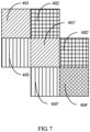
FIG. 7 is still another diagram of comparison of relative positions between a pixel region in which a first sub-pixel region is located and a pixel region in which a second sub-pixel region is located in a camera module according to an embodiment of this application. - Reference numerals in the accompanying drawings are as follows:
- 100: housing;
- 200: lens;
- 400: photosensitive chip; 401: first sub-pixel region; 402: second sub-pixel region; 403: third sub-pixel region; 404: fourth sub-pixel region; 401': first sub-pixel region; 402': second sub-pixel region; 403': third sub-pixel region; 404': fourth sub-pixel region;
- 500: infrared cut-off filter;
- 600: limiting member; 601: limiting base; 602: connecting component; 603: movable space.
- To make the objectives, technical solutions, and advantages of this application clearer, the following clearly and completely describes the technical solutions of this application with reference to the specific embodiments of this application and the corresponding accompanying drawings. Apparently, the described embodiments are merely some rather than all of embodiments of this application. All other embodiments obtained by a person of ordinary skill in the art based on embodiments of this application without creative efforts shall fall within the protection scope of this application.
- The technical solutions disclosed in embodiments of this application are described in detail below with reference to the accompanying drawings.
- As shown in
FIG. 1 to FIG. 3 , this application discloses a camera module. The camera module includes alens 200, a driving member, and aphotosensitive chip 400. In addition, the camera module further includes ahousing 100. All the foregoing devices can be installed on thehousing 100. Thehousing 100 may be made from a material such as plastic or metal. Certainly, the camera module may be alternatively provided with another structure. For brevity, details are not described herein again. - The
photosensitive chip 400 is an imaging sensor, and thephotosensitive chip 400 is a Bayer array sensor, that is, photosensitive pixels in thephotosensitive chip 400 are arranged in a manner of a Bayer array. Thephotosensitive chip 400 includes a plurality of pixel regions arranged in rows and columns, each pixel region includes four sub-pixel regions, and the four sub-pixel regions are arranged in a 2×2 matrix. The four sub-pixel regions may include two green pixels, one blue pixel, and one red pixel, and the two green pixels are arranged diagonally. The four sub-pixel regions in each pixel region may be respectively a first sub-pixel region, a second sub-pixel region, a third sub-pixel region, and a fourth sub-pixel region. - In general, the
photosensitive chip 400 may include a filtering array layer and a photosensitive layer. Light passes through the filtering array layer and shine on the photosensitive layer. The filtering array layer can filter colors, which can make the light that passes through the filtering array layer retain only one color such as red, blue, or green. - As mentioned above, the
photosensitive chip 400 includes the plurality of pixel regions, and each pixel region includes the four sub-pixel regions. In detail, each sub-pixel region is a part of thephotosensitive chip 400, that is, each sub-pixel region may include a filtering sublayer and a photosensitive sublayer, and there is a plurality of sub-pixel regions. Further, all filtering sublayers form the filtering array layer, and all photosensitive sublayers form the photosensitive layer. - In the filtering array layer of the Bayer array sensor, a part corresponding to each pixel region is provided with four filters, and the four filters correspond to four sub-pixel regions respectively in one pixel region. In addition, the above four filters usually include a red light filter, a blue light filter, and two green light filters, and the four filters are referred to as RGGB for short. In a case that types of the filters disposed in different sub-pixel regions of the photosensitive layer are different, colors of images formed by the regions corresponding to the different sub-pixel regions of the photosensitive layer are also different.
- In the camera module provided in this embodiment of this application, the
photosensitive chip 400 is connected to the driving member, and the driving member can drive thephotosensitive chip 400 to move relative to thelens 200. Thelens 200 can be kept fixed, and only thephotosensitive chip 400 is controlled to move, so as to improve control accuracy, and reduce control difficulty. - Specifically, the
lens 200 may be fixedly connected to thehousing 100, and thephotosensitive chip 400 can form a movable connection relationship with thehousing 100 through the driving member. Thelens 200 may be fixed on thehousing 100 in a manner such as bonding. The driving member may be a miniature linear motor, and the like. The driving member may be installed on thehousing 100 through a connecting component such as a screw, and thephotosensitive chip 400 may be connected to a driving head of the driving member, so that the driving member can drive thephotosensitive chip 400 to move relative to thehousing 100, that is, thephotosensitive chip 400 and thelens 200 can generate relative movement. - More specifically, the driving member can drive the
photosensitive chip 400 to switch between a first position and a second position relative to thelens 200. In the foregoing case, a relative position between thelens 200 and thephotosensitive chip 400 can be changed by adjusting the position of thephotosensitive chip 400, so that the light incident from a same position on thelens 200 can be projected in different positions on thephotosensitive chip 400, and images with same content are formed in different positions on thephotosensitive chip 400. - In a case that the
photosensitive chip 400 is in the first position, the light incident from thelens 200 forms a first image in the first sub-pixel region of thephotosensitive chip 400. In a case that thephotosensitive chip 400 is in the second position, the light incident from thelens 200 forms a second image in the second sub-pixel region of thephotosensitive chip 400. - It should be noted that after one of the first image and the second image is formed, and the driving member works to drive the
photosensitive chip 400 to change the position thereof, the other image is formed. Thephotosensitive chip 400 may have a specific displacement between the two imaging processes relative to a framing region. However, edges of the image formed on thephotosensitive chip 400 are not displayed in a finally-edited image, and the displacement of thephotosensitive chip 400 is extremely small. Therefore, in a case that the camera module remains fixed as a whole, it can be considered that content of the images formed after the two imaging processes is basically the same, and further, it can be ensured that the content of the first image and the content of the second image formed in one sub-pixel region of thephotosensitive chip 400 are the same. - Because the relative position between the
lens 200 and thephotosensitive chip 400 changes during the formation of the first image and the second image, the positions in which the light projected on thephotosensitive chip 400 through thelens 200 can also change, that is, the first image is formed in the first sub-pixel region of thephotosensitive chip 400, and the secondphotosensitive chip 400 is formed in the second sub-pixel region of thephotosensitive chip 400. - In a case that the displacement of the
photosensitive chip 400 is different, an interval between the first sub-pixel region and the second sub-pixel region is also different, so that there may be a case that the first sub-pixel region and the second sub-pixel region are not located in the same pixel region. However, even if the first sub-pixel region and the second sub-pixel region are located in two pixel regions respectively, because both the first sub-pixel region and the second sub-pixel region corresponds to filters, and structures of the plurality of pixel regions on thephotosensitive chip 400 are the same, the pixel region in which the first sub-pixel region is located includes a sub-pixel region having a filter that is the same as the filter corresponding to the second sub-pixel region. Accordingly, the pixel region in which the second sub-pixel region is located also includes a sub-pixel region having a filter that is the same as the filter corresponding to the first sub-pixel region. Therefore, the first sub-pixel region may be equivalent to another sub-pixel region in the pixel region in which the second sub-pixel region is located. The equivalent sub-pixel regions of the first sub-pixel region and the second sub-pixel region in the same pixel region are any two sub-pixel regions in the pixel region, that is, the first sub-pixel region is certainly not equivalent to the second sub-pixel region when the first sub-pixel region is equivalently located in the pixel region in which the second sub-pixel region is located. Accordingly, the second sub-pixel region is certainly not equivalent to the first sub-pixel region when the second sub-pixel region is equivalently located in the pixel region in which the first sub-pixel region is located. - In a case that the foregoing technical solution is used, the foregoing light incident from the center of the
lens 200 is used as an example, and the light is projected on thephotosensitive chip 400 through thelens 200 to form the first image. Then, thephotosensitive chip 400 is driven to move, so that the light incident from the center of thelens 200 is projected on thephotosensitive chip 400 again, to form the second image. - A displacement and a displacement direction of the
photosensitive chip 400 may be designed. That is, the foregoing light can be projected to a first sub-pixel region corresponding to a red filter in thephotosensitive chip 400 in the first position through thelens 200, and the foregoing light can be projected to a second sub-pixel region corresponding to a green filter in thephotosensitive chip 400 in the second position through thelens 200. Alternatively, the foregoing light can first be projected to the first sub-pixel region corresponding to a blue filter in thephotosensitive chip 400, and then to the second sub-pixel region corresponding to the green filter in thephotosensitive chip 400. Alternatively, the foregoing light can first be projected to a first sub-pixel region corresponding to a first green filter in thephotosensitive chip 400, and then to a second sub-pixel region corresponding to a second green filter in thephotosensitive chip 400. A red filter is adjacent to a lower part of the first green filter, a blue filter is adjacent to a right part of the first green filter, while a red filter is adjacent to an upper part of the second green filter, and a blue filter is adjacent to a left part of the second green filter. That is, a position of the first green filter is different from that of the second green filter in one pixel region. - In conclusion, a filter processing result of the foregoing light by a filter corresponding to the first sub-pixel region in the
photosensitive chip 400 is different from a filtering processing result of the foregoing light by a filter corresponding to the second sub-pixel region in thephotosensitive chip 400, so that the same light can be processed separately by two types of filters, and two images with the same content but different colors are formed. The first image and the second image are synthesized by using a preset algorithm, so that real photosensitive pixels of each filter channel on the synthesized image can be increased, and resolution of the image is improved, thereby making photos present better, and improving final image quality and user experience. - As mentioned above, the displacement and a displacement direction of the
photosensitive chip 400 may be designed so that the first image and the second image formed have the same content but different colors. More specifically, the displacement of thephotosensitive chip 400 may be a side length of the sub-pixel region, and the displacement direction of thephotosensitive chip 400 may be an extending direction of an edge of the sub-pixel region, or the displacement of thephotosensitive chip 400 may be the sum of the side length of the sub-pixel region and the side lengths of n pixel regions, where n is an integer, and n≥0. - In addition, moving directions of the
photosensitive chip 400 may be determined according to an actual situation. For example, thephotosensitive chip 400 may generate a displacement of the side length of a sub-pixel region leftward in a plane perpendicular to an optical axis of the photosensitive chip, or thephotosensitive chip 400 may generate a displacement of the side length of a sub-pixel region downward in a plane perpendicular to an optical axis of the photosensitive chip, or thephotosensitive chip 400 may generate a displacement of a size of a diagonal of a sub-pixel region toward the lower left in a plane perpendicular to an optical axis of the photosensitive chip. This is not limited herein. In addition, in a case that the moving directions of thephotosensitive chip 400 are different, types of the filters corresponding to the first sub-pixel region and the second sub-pixel region are also different. - More intuitively, as shown in
FIG. 4, FIG. 4 shows distribution of the four sub-pixel regions in each pixel region of thephotosensitive chip 400, namely, a firstsub-pixel region 401, a secondsub-pixel region 402, a thirdsub-pixel region 403, and a fourthsub-pixel region 404. The firstsub-pixel region 401 of thephotosensitive chip 400 in the first position faces the center of thelens 200. That is, in a case that thephotosensitive chip 400 is in the first position, the light incident from the center of thelens 200 may be projected to the firstsub-pixel region 401. Correspondingly, after the position of thephotosensitive chip 400 changes, a correspondence between thelens 200 and thephotosensitive chip 400 also changes. Specifically, after thephotosensitive chip 400 moves to the second position, a second sub-pixel region 402' faces the center of thelens 200. That is, in a case that thephotosensitive chip 400 is in the second position, the light incident from the center of thelens 200 may be projected to the second sub-pixel region 402'. Although the second sub-pixel region 402' and the secondsub-pixel region 402 may correspond to the same type filter, the two sub-pixel regions may also be respectively located in two pixel regions, and a pixel region in which the second sub-pixel region 402' is located further includes a first sub-pixel region 401', a third sub-pixel region 403', and a fourth sub-pixel region 404'. - In a process of driving the
photosensitive chip 400 to move, thephotosensitive chip 400 may generate a displacement of the side length of a sub-pixel region leftward or downward in the plane perpendicular to the optical axis of the photosensitive chip, or generate a displacement of a length of a diagonal of a sub-pixel region toward the lower left in the plane perpendicular to the optical axis of the photosensitive chip, so that the relative positions between the pixel region where the firstsub-pixel region 401 is located and the pixel region where the second sub-pixel region 402' is located separately correspond toFIG. 5 to FIG. 7 . - This embodiment of this application provides the camera module. The lens of the camera module fits the photosensitive chip, and the
photosensitive chip 400 can switch between the first position and the second position, so that the first image and the second image can be respectively formed in the first sub-pixel region and the second sub-pixel region of the photosensitive chip in a case that a position of thephotosensitive chip 400 changes. The content of the first image and the content of the second image are the same. In addition, the equivalent sub-pixel regions of the first sub-pixel region and the second sub-pixel region in the same pixel region are any two of the pixel regions, so that filtering processing results of the incident light by the photosensitive chip are different during the two imaging processes. Further, the first image and the second image are synthesized by using a preset algorithm, so that real photosensitive pixels of each filter channel on the formed synthesized image can be increased, and resolution of the image is improved, thereby making photos present better, and improving final image quality and user experience. - Optionally, in the camera module provided in this embodiment of this application, the driving member may alternatively drive the
photosensitive chip 400 to a third position. That is, the driving member may drive thephotosensitive chip 400 to switch between the first position, the second position, and the third position relative to thelens 200. Specifically, there are a plurality of the driving members, or the driving member can provide driving forces in different directions. In a case that thephotosensitive chip 400 is in the third position, the light incident from thelens 200 forms a third image in a third sub-pixel region of thephotosensitive chip 400, content of the third image and content of the first image are the same, and equivalent sub-pixel regions of the first sub-pixel region, the second sub-pixel region, and the third sub-pixel region in the same pixel region are any three of the sub-pixel regions in the pixel region. - By using the foregoing technical solution, types of the filter processing results of the same light can be increased. After the first image, the second image, and the third image are synthesized by the preset algorithm, the real photosensitive pixels of each filter channel on the synthesized image can be further increased to further improve resolution of the image. Specifically, by controlling the moving directions of the
photosensitive chip 400, the relative position relationship between thephotosensitive chip 400 and thelens 200 can be changed, and then the sub-pixel region corresponding to the light incident from thelens 200 can be changed. That is, the type of the filter through which the light incident from thelens 200 passes can be changed, so as to enhance the filtering processing results of the same light. Optionally, the first sub-pixel region, the second sub-pixel region, and the third sub-pixel region can correspond to the green filter, the red filter, and the blue filter respectively, so that the resolution of the photosensitive pixels corresponding to RGB in the image can be improved, thereby making the formed image better. - Further, in the camera module provided in this embodiment of this application, the driving member can also drive the
photosensitive chip 400 to move to a fourth position. That is, the driving member can drive thephotosensitive chip 400 to switch between the first position, the second position, the third position, and the fourth position relative to thelens 200. In a case that thephotosensitive chip 400 is in the fourth position, the light incident from thelens 200 forms a fourth image in a fourth sub-pixel region of thephotosensitive chip 400, content of the fourth image and content of the first image are the same, and equivalent sub-pixel regions of the first sub-pixel region, the second sub-pixel region, the third sub-pixel region, and the fourth sub-pixel region in the same pixel region are four of the sub-pixel regions in the pixel region. - By using the foregoing technical solution, types of the filter processing results of the same light can be increased. After the first image, the second image, the third image, and the fourth image are synthesized by the preset algorithm, the real photosensitive pixels of each filter channel on the synthesized image can be further increased to further improve resolution of the image. When the foregoing technical solution is used, compared with the solution in which the light is directly incident on the photosensitive chip, resolution of an R image and a B image is tripled, and resolution of a G image is doubled, thereby greatly improving resolution of the image.
- In a process in which the driving member drives the
photosensitive chip 400 to move, by precisely controlling a driving amount of the driving member, it can be ensured that thephotosensitive chip 400 can move a preset displacement when moving, and the preset displacement can be a side length of a sub-pixel region. To reduce difficulty of controlling the camera module, in another embodiment of this application, optionally, the camera module further includes a limitingmember 600, and the photosensitive chip is in movable fit with the lens through the limiting member. - The limiting
member 600 includes a limitingbase 601 and a connectingcomponent 602, and the limitingbase 601 is movably connected to the connectingcomponent 602. Thephotosensitive chip 400 and the driving head of the driving member may both be connected to the limitingbase 601, or may both be connected to the connectingcomponent 602, so that the displacement of thephotosensitive chip 400 can be controlled by a limiting fit relationship between the limitingbase 601 and the connectingcomponent 602. For example, the limitingbase 601 can be fastened onto thehousing 100, and thephotosensitive chip 400 and the driving head of the driving member are both connected to the connectingcomponent 602. - The limiting
base 601 is provided with a first limiting groove, a second limiting groove, a third limiting groove, and a fourth limiting groove. The first limiting groove, the second limiting groove, the third limiting groove, and the fourth limiting groove are connected to each other to form amovable space 603, so as to ensure that the connectingcomponent 602 can move in the movable space and is in limiting fit with the above four limiting grooves. - Moreover, in a case that the connecting
component 602 is limited in the first limiting groove, thephotosensitive chip 400 is located in the first position; in a case that the connectingcomponent 602 is limited in the second limiting groove, thephotosensitive chip 400 is located in the second position; in a case that the connectingcomponent 602 is limited in the third limiting groove, thephotosensitive chip 400 is located in the third position; and in a case that the connectingcomponent 602 is limited in the fourth limiting groove, thephotosensitive chip 400 is located in the fourth position. - Usually, by using the foregoing technical solution, the displacement of the
photosensitive chip 400 may be limited by the limitingmember 600. When thephotosensitive chip 400 needs to be moved, the connecting component is driven to move to a corresponding position by the driving member, and the limitingbase 601 can provide a reliable limiting function, so that when the connecting component cannot continue to move in the corresponding direction, it can be considered that thephotosensitive chip 400 has been driven to a target position, which reduces difficulty of controlling the driving amount of the driving member by the driving member. - Specifically, specific sizes and structures of the first limiting groove, the second limiting groove, the third limiting groove, and the fourth limiting groove may be determined according to an actual condition such as a size and shape of the connecting component. Optionally, the first limiting groove, the second limiting groove, the third limiting groove, and the fourth limiting groove may all be square mechanical parts, and sizes thereof are the same as that of the sub-pixel region. Correspondingly, to ensure that the connecting component can be normally limited, the connecting component can also be a cylindrical structure with a square bottom.
- Optionally, the four limiting grooves may be connected to each other to form a square structure, that is, the four limiting grooves respectively correspond to the four sub-pixel regions in the pixel region, and are distributed in a 2×2 form. In this case, when the connecting
component 602 and the four limiting grooves are in fit with each other, thephotosensitive chip 400 may be separately located in the first position, the second position, the third position, and the fourth position, thereby separately forming the first image, the second image, the third image, and the fourth image on thephotosensitive chip 400. - In another embodiment of this application, the second limiting groove is connected to the third limiting groove, the first limiting groove is located on one side along an arranging direction of the second limiting groove and the third limiting groove, and the fourth limiting groove is located on the other side of the arranging direction. The first limiting groove is connected to the second limiting groove, and the fourth limiting groove is connected to the third limiting groove. In general, it can be considered that the second limiting groove is connected to the right part of the first limiting groove, the third limiting groove is connected to the lower part of the second limiting groove, and the fourth limiting groove is connected to the right part of the third limiting groove, so as to form a Z-shaped structure.
- In a case that the foregoing technical solution is used, when the connecting
component 602 moves between any adjacent two of the foregoing four limiting grooves, the connectingcomponent 602 can be limited by the limitingbase 601 in a certain direction, and by combining driving forces provided by the driving member, the moving direction of the connectingcomponent 602 can be made unique, further reducing the driving difficulty and improving the movement precision. - As described above, a size of the first limiting groove and the like on the limiting base may be determined based on parameters such as the structure and size of the connecting component. Optionally, in the arranging direction of the first limiting groove and the second limiting groove, and in the arranging direction of the second limiting groove and the third limiting groove, the size of the connecting component is equal to the size of the sub-pixel region. In this case, the shapes and sizes of bottom surfaces of the first limiting groove, the second limiting groove, the third limiting groove, and the fourth limiting groove are the same as the shape and size of the sub-pixel region respectively correspondingly, so that design and processing difficulty of the first limiting groove and the like are lower, and it can be ensured that there is a more reliable limiting relationship between the connecting component and each limiting groove. Specifically, the connecting component may be a cylindrical-shaped mechanical part with a square bottom. In another embodiment of this application, the connecting
component 602 may be a cylindrical-shaped mechanical part. In this case, a contact area between the connectingcomponent 602 and the limitingbase 601 is small, which can reduce the difficulty of their relative movement and difficulty of driven movements. - The optical axis of the lens is perpendicular to a photosensitive surface of the
photosensitive chip 400, that is, the photosensitive chip faces the lens. In this case, design and installation difficulty of the lens and the photosensitive chip are lower, sensitivity of thephotosensitive chip 400 may be improved, and imaging quality is improved. Certainly, in a case that here is a corresponding requirement, thephotosensitive chip 400 may unnecessarily be opposite thelens 200. For example, the camera module may be set as a periscope module, which can improve a zoom ratio of the camera module. - Optionally, the camera module provided in this embodiment of this application further includes an infrared cut-
off filter 500. The infrared cut-off filter 500 is disposed on an out-light side of the lens, that is, on a light input side of thephotosensitive chip 400. The infrared cut-off filter 500 can provide a filtering effect for light incident into the camera module through thelens 200, thereby filtering out unnecessary light projected into thephotosensitive chip 400, preventing thephotosensitive chip 400 from producing false colors and/or ripples, and improving the effective resolution and color reproduction of thephotosensitive chip 400. - Optionally, the
lens 200 is an extended depth of field lens. Passing focuses of R, G, and B filter channels of thelens 200 are designed to be located at different positions, and the three passing focuses cover three focal segments, so that longitudinal chromatic aberration of the R, G, and B bands is enlarged to cover far, middle, and near distances. The far, middle, and near distances are relative concepts. That is, the far distance is a greater distance compared with the middle distance, and the near distance is a shorter distance compared with the middle distance. - The
lens 200 uses the foregoing technical solution, three photos correspond to R, G, and B, and the three photos focus on the foregoing three distances, namely, far, middle, and near. After this, based on a restoration algorithm, a window detection function may be used to detect the entire field of view region, and determine which of the three photos corresponding to R, G, and B in each window is the clearest. Then, based on the clearest photo, the other two photos can be used for resolution transformation with the help of a deconvolution algorithm to synthesize photos that are relatively clear in any distance. - On the basis of the camera module disclosed in any of the foregoing embodiments, an embodiment of this application further provides an electronic device, the electronic device includes the camera module provided in any of the foregoing embodiments, and certainly, the electronic device further includes a display module, a housing, a battery, and other devices. For brevity, details are not described herein again.
- The electronic device disclosed in embodiments of this application may be a smart phone, a tablet computer, an e-book reader, or a wearable device. Certainly, the electronic device may also be another device. This is not limited in embodiments of this application.
- The foregoing embodiments of this application focus on describing differences between the embodiments, and different optimization features of the embodiments may be combined to form better embodiments provided that they are not contradictory. For brevity, details are not described herein again.
- The foregoing descriptions are merely embodiments of this application, and are not intended to limit this application. Various changes and modifications may be made to this application by a person skilled in the art. Any modifications, equivalent substitutions, improvements, and the like made within the spirit and principle of this application should be included within the scope of the claims of this application.
Claims (10)
- A camera module, comprising a lens, a driving member, and a photosensitive chip, wherein the photosensitive chip is a Bayer array sensor, the photosensitive chip comprises a plurality of pixel regions arranged in rows and columns, and each of the pixel regions includes four sub-pixel regions;the photosensitive chip is connected to the driving member, and the driving member drives the photosensitive chip to switch between a first position and a second position relative to the lens; andin a case that the photosensitive chip is in the first position, light incident from the lens forms a first image in a first sub-pixel region of the photosensitive chip; in a case that the photosensitive chip is in the second position, light incident from the lens forms a second image in a second sub-pixel region of the photosensitive chip; and content of the first image and content of the second image are same, and equivalent sub-pixel regions of the first sub-pixel region and the second sub-pixel region in a same pixel region are any two of the sub-pixel regions in the pixel region.
- The camera module according to claim 1, wherein the driving member drives the photosensitive chip to switch between the first position, the second position, and a third position relative to the lens; and
in a case that the photosensitive chip is in the third position, light incident from the lens forms a third image in a third sub-pixel region of the photosensitive chip; and content of the third image and the content of the first image are same, and equivalent sub-pixel regions of the first sub-pixel region, the second sub-pixel region, and the third sub-pixel region in a same pixel region are any three of the sub-pixel regions in the pixel region. - The camera module according to claim 2, wherein the driving member drives the photosensitive chip to switch between the first position, the second position, the third position, and a fourth position relative to the lens; and
in a case that the photosensitive chip is in the fourth position, light incident from the lens forms a fourth image in a fourth sub-pixel region of the photosensitive chip; content of the fourth image and the content of the first image are same, and equivalent sub-pixel regions of the first sub-pixel region, the second sub-pixel region, the third sub-pixel region, and the fourth sub-pixel region in a same pixel region are four of the sub-pixel regions in the pixel region. - The camera module according to claim 3, wherein the camera module further comprises a limiting member, the photosensitive chip is in movable fit with the lens through the limiting member, the limiting member comprises a limiting base and a connecting component, and the limiting base or the connecting component is connected to the driving member; and
the limiting base is provided with a first limiting groove, a second limiting groove, a third limiting groove, and a fourth limiting groove that communicate with each other, wherein in a case that the connecting component is limited in the first limiting groove, the lens is in the first position; in a case that the connecting component is limited in the second limiting groove, the lens is in the second position; in a case that the connecting component is limited in the third limiting groove, the lens is in the third position; and in a case that the connecting component is limited in the fourth limiting groove, the lens is in the fourth position. - The camera module according to claim 4, wherein the second limiting groove is connected to the third limiting groove, the first limiting groove is located on one side of an arranging direction of the second limiting groove and the third limiting groove, the fourth limiting groove is located on the other side of the arranging direction, the first limiting groove is connected to the second limiting groove, and the fourth limiting groove is connected to the third limiting groove.
- The camera module according to claim 4, wherein in an arranging direction of the first limiting groove and the second limiting groove, and in an arranging direction of the second limiting groove and the third limiting groove, a size of the connecting component is equal to a side length of one sub-pixel region.
- The camera module according to claim 6, wherein the connecting component is a cylindrical-shaped mechanical part.
- The camera module according to claim 1, wherein the camera module further comprises an infrared cut-off filter, and the infrared cut-off filter is disposed on an out-light side of the lens.
- The camera module according to claim 1, wherein the lens is an extended depth of field lens.
- An electronic device, comprising the camera module according to any one of claims 1 to 9.
Applications Claiming Priority (2)
| Application Number | Priority Date | Filing Date | Title |
|---|---|---|---|
| CN202011639272.8A CN112616007B (en) | 2020-12-31 | 2020-12-31 | Electronic equipment and camera module thereof |
| PCT/CN2021/142408 WO2022143747A1 (en) | 2020-12-31 | 2021-12-29 | Electronic device and photographing module thereof |
Publications (3)
| Publication Number | Publication Date |
|---|---|
| EP4254932A1 true EP4254932A1 (en) | 2023-10-04 |
| EP4254932A4 EP4254932A4 (en) | 2024-04-03 |
| EP4254932B1 EP4254932B1 (en) | 2025-05-07 |
Family
ID=75253210
Family Applications (1)
| Application Number | Title | Priority Date | Filing Date |
|---|---|---|---|
| EP21914479.7A Active EP4254932B1 (en) | 2020-12-31 | 2021-12-29 | Electronic device and photographing module thereof |
Country Status (6)
| Country | Link |
|---|---|
| US (1) | US12506944B2 (en) |
| EP (1) | EP4254932B1 (en) |
| JP (1) | JP7610008B2 (en) |
| CN (1) | CN112616007B (en) |
| ES (1) | ES3032486T3 (en) |
| WO (1) | WO2022143747A1 (en) |
Families Citing this family (1)
| Publication number | Priority date | Publication date | Assignee | Title |
|---|---|---|---|---|
| CN112616007B (en) * | 2020-12-31 | 2022-06-17 | 维沃移动通信有限公司 | Electronic equipment and camera module thereof |
Family Cites Families (25)
| Publication number | Priority date | Publication date | Assignee | Title |
|---|---|---|---|---|
| US5182652A (en) * | 1991-09-06 | 1993-01-26 | Eastman Kodak Company | High resolution thermal printing by imaging a hard copy image in vertical and horizontal increments smaller than the pixel pitch of a video imager array |
| US5335091A (en) * | 1991-12-31 | 1994-08-02 | Eastman Kodak Company | Apparatus for mechanically dithering a CCD array |
| US6195125B1 (en) * | 1995-08-11 | 2001-02-27 | Canon Kabushiki Kaisha | Pixel shifting image sensor with a different number of images sensed in each mode |
| JPH09219867A (en) * | 1995-11-10 | 1997-08-19 | Techno Media:Kk | Still color picture image pickup device and its method |
| WO1997017811A1 (en) * | 1995-11-10 | 1997-05-15 | Techno Media Co., Ltd. | Method and device for picking up color still image |
| IL126165A0 (en) * | 1998-09-10 | 1999-05-09 | Scitex Corp Ltd | Apparatus for the orthogonal movement of a ccd sensor |
| JP4158280B2 (en) * | 1999-06-04 | 2008-10-01 | ソニー株式会社 | Image processing apparatus and method |
| JP2002159014A (en) * | 2000-11-21 | 2002-05-31 | Hitachi Ltd | Image generation apparatus and generation method |
| JP2007235911A (en) * | 2006-02-03 | 2007-09-13 | Rohm Co Ltd | Camera module and image reader using same |
| CN101533205B (en) * | 2008-03-13 | 2012-10-03 | Hoya株式会社 | Imaging device |
| KR101499540B1 (en) * | 2008-10-24 | 2015-03-06 | 삼성전자주식회사 | Image pickup apparatus and image processing method using the same |
| JP5707792B2 (en) * | 2010-09-08 | 2015-04-30 | 富士通株式会社 | Real-time depth-of-field extension system and real-time depth-of-field extension method |
| US9106784B2 (en) * | 2013-03-13 | 2015-08-11 | Pelican Imaging Corporation | Systems and methods for controlling aliasing in images captured by an array camera for use in super-resolution processing |
| US8917327B1 (en) * | 2013-10-04 | 2014-12-23 | icClarity, Inc. | Method to use array sensors to measure multiple types of data at full resolution of the sensor |
| CN104079904A (en) * | 2014-07-17 | 2014-10-01 | 广东欧珀移动通信有限公司 | A color image generation method and device |
| KR102469426B1 (en) * | 2015-10-27 | 2022-11-22 | 삼성전자주식회사 | Image processing apparatus and operating method thereof |
| JP2019145856A (en) * | 2016-06-27 | 2019-08-29 | 富士フイルム株式会社 | Imaging device and method for controlling the same |
| WO2018003501A1 (en) * | 2016-06-28 | 2018-01-04 | ソニー株式会社 | Solid-state imaging device, electronic apparatus, lens control method, and vehicle |
| CN106210677B (en) * | 2016-07-29 | 2018-02-06 | 广东欧珀移动通信有限公司 | Image color processing method and device and terminal equipment |
| US10369832B2 (en) * | 2016-10-14 | 2019-08-06 | Lumenco, Llc | Optical security elements with opaque masks for enhanced lens-to-printed pixel alignment |
| CN109655989B (en) * | 2017-10-11 | 2024-05-03 | 宁波舜宇光电信息有限公司 | Actuator for optical assembly and corresponding camera module |
| US10687033B2 (en) * | 2018-09-24 | 2020-06-16 | Google Llc | Color imaging system |
| JP2020123862A (en) * | 2019-01-31 | 2020-08-13 | キヤノン株式会社 | Image coding device |
| JP7247682B2 (en) * | 2019-03-18 | 2023-03-29 | 株式会社リコー | Image processing device, image processing method, image processing program, electronic device, and photographing device |
| CN112616007B (en) * | 2020-12-31 | 2022-06-17 | 维沃移动通信有限公司 | Electronic equipment and camera module thereof |
-
2020
- 2020-12-31 CN CN202011639272.8A patent/CN112616007B/en active Active
-
2021
- 2021-12-29 JP JP2023539310A patent/JP7610008B2/en active Active
- 2021-12-29 WO PCT/CN2021/142408 patent/WO2022143747A1/en not_active Ceased
- 2021-12-29 EP EP21914479.7A patent/EP4254932B1/en active Active
- 2021-12-29 ES ES21914479T patent/ES3032486T3/en active Active
-
2023
- 2023-06-29 US US18/216,572 patent/US12506944B2/en active Active
Also Published As
| Publication number | Publication date |
|---|---|
| ES3032486T3 (en) | 2025-07-21 |
| JP2024501031A (en) | 2024-01-10 |
| EP4254932B1 (en) | 2025-05-07 |
| US20230345102A1 (en) | 2023-10-26 |
| WO2022143747A1 (en) | 2022-07-07 |
| CN112616007B (en) | 2022-06-17 |
| CN112616007A (en) | 2021-04-06 |
| US12506944B2 (en) | 2025-12-23 |
| JP7610008B2 (en) | 2025-01-07 |
| EP4254932A4 (en) | 2024-04-03 |
Similar Documents
| Publication | Publication Date | Title |
|---|---|---|
| US9838601B2 (en) | Multi-camera system using folded optics | |
| US11703668B2 (en) | Zoom dual-aperture camera with folded lens | |
| US12356060B2 (en) | Electronic device and photographing module thereof | |
| US12506944B2 (en) | Electronic device, and camera module thereof with movable photosensitive ship | |
| US12598368B2 (en) | Electronic device, and camera module thereof wherein a lens is in moveable fit with a limiting member having first through fourth limiting grooves in communication with each other | |
| US12470841B2 (en) | Electronic device and camera module thereof | |
| US12328493B2 (en) | Electronic device using multi-frame composition method | |
| CN112788218B (en) | Electronic equipment and camera module thereof | |
| CN112822367B (en) | Electronic equipment and camera module thereof |
Legal Events
| Date | Code | Title | Description |
|---|---|---|---|
| STAA | Information on the status of an ep patent application or granted ep patent |
Free format text: STATUS: THE INTERNATIONAL PUBLICATION HAS BEEN MADE |
|
| PUAI | Public reference made under article 153(3) epc to a published international application that has entered the european phase |
Free format text: ORIGINAL CODE: 0009012 |
|
| STAA | Information on the status of an ep patent application or granted ep patent |
Free format text: STATUS: REQUEST FOR EXAMINATION WAS MADE |
|
| 17P | Request for examination filed |
Effective date: 20230628 |
|
| AK | Designated contracting states |
Kind code of ref document: A1 Designated state(s): AL AT BE BG CH CY CZ DE DK EE ES FI FR GB GR HR HU IE IS IT LI LT LU LV MC MK MT NL NO PL PT RO RS SE SI SK SM TR |
|
| REG | Reference to a national code |
Ref country code: DE Free format text: PREVIOUS MAIN CLASS: H04N0005225000 Ref country code: DE Ref legal event code: R079 Ref document number: 602021030619 Country of ref document: DE Free format text: PREVIOUS MAIN CLASS: H04N0005225000 Ipc: H04N0023540000 |
|
| A4 | Supplementary search report drawn up and despatched |
Effective date: 20240304 |
|
| DAV | Request for validation of the european patent (deleted) | ||
| DAX | Request for extension of the european patent (deleted) | ||
| RIC1 | Information provided on ipc code assigned before grant |
Ipc: H04N 23/951 20230101ALI20240227BHEP Ipc: H04N 25/48 20230101ALI20240227BHEP Ipc: H04N 23/57 20230101ALI20240227BHEP Ipc: H04N 23/54 20230101AFI20240227BHEP |
|
| GRAP | Despatch of communication of intention to grant a patent |
Free format text: ORIGINAL CODE: EPIDOSNIGR1 |
|
| STAA | Information on the status of an ep patent application or granted ep patent |
Free format text: STATUS: GRANT OF PATENT IS INTENDED |
|
| GRAS | Grant fee paid |
Free format text: ORIGINAL CODE: EPIDOSNIGR3 |
|
| RIC1 | Information provided on ipc code assigned before grant |
Ipc: H04M 1/02 20060101ALI20250225BHEP Ipc: H04N 25/48 20230101ALI20250225BHEP Ipc: H04N 23/951 20230101ALI20250225BHEP Ipc: H04N 23/57 20230101ALI20250225BHEP Ipc: H04N 23/54 20230101AFI20250225BHEP |
|
| GRAA | (expected) grant |
Free format text: ORIGINAL CODE: 0009210 |
|
| STAA | Information on the status of an ep patent application or granted ep patent |
Free format text: STATUS: THE PATENT HAS BEEN GRANTED |
|
| INTG | Intention to grant announced |
Effective date: 20250310 |
|
| AK | Designated contracting states |
Kind code of ref document: B1 Designated state(s): AL AT BE BG CH CY CZ DE DK EE ES FI FR GB GR HR HU IE IS IT LI LT LU LV MC MK MT NL NO PL PT RO RS SE SI SK SM TR |
|
| REG | Reference to a national code |
Ref country code: GB Ref legal event code: FG4D |
|
| REG | Reference to a national code |
Ref country code: CH Ref legal event code: EP |
|
| REG | Reference to a national code |
Ref country code: DE Ref legal event code: R096 Ref document number: 602021030619 Country of ref document: DE |
|
| REG | Reference to a national code |
Ref country code: IE Ref legal event code: FG4D |
|
| REG | Reference to a national code |
Ref country code: NL Ref legal event code: FP |
|
| REG | Reference to a national code |
Ref country code: ES Ref legal event code: FG2A Ref document number: 3032486 Country of ref document: ES Kind code of ref document: T3 Effective date: 20250721 |
|
| PG25 | Lapsed in a contracting state [announced via postgrant information from national office to epo] |
Ref country code: PT Free format text: LAPSE BECAUSE OF FAILURE TO SUBMIT A TRANSLATION OF THE DESCRIPTION OR TO PAY THE FEE WITHIN THE PRESCRIBED TIME-LIMIT Effective date: 20250908 Ref country code: FI Free format text: LAPSE BECAUSE OF FAILURE TO SUBMIT A TRANSLATION OF THE DESCRIPTION OR TO PAY THE FEE WITHIN THE PRESCRIBED TIME-LIMIT Effective date: 20250507 |
|
| REG | Reference to a national code |
Ref country code: LT Ref legal event code: MG9D |
|
| PG25 | Lapsed in a contracting state [announced via postgrant information from national office to epo] |
Ref country code: GR Free format text: LAPSE BECAUSE OF FAILURE TO SUBMIT A TRANSLATION OF THE DESCRIPTION OR TO PAY THE FEE WITHIN THE PRESCRIBED TIME-LIMIT Effective date: 20250808 Ref country code: NO Free format text: LAPSE BECAUSE OF FAILURE TO SUBMIT A TRANSLATION OF THE DESCRIPTION OR TO PAY THE FEE WITHIN THE PRESCRIBED TIME-LIMIT Effective date: 20250807 |
|
| PG25 | Lapsed in a contracting state [announced via postgrant information from national office to epo] |
Ref country code: PL Free format text: LAPSE BECAUSE OF FAILURE TO SUBMIT A TRANSLATION OF THE DESCRIPTION OR TO PAY THE FEE WITHIN THE PRESCRIBED TIME-LIMIT Effective date: 20250507 |
|
| REG | Reference to a national code |
Ref country code: AT Ref legal event code: MK05 Ref document number: 1793812 Country of ref document: AT Kind code of ref document: T Effective date: 20250507 |
|
| PG25 | Lapsed in a contracting state [announced via postgrant information from national office to epo] |
Ref country code: BG Free format text: LAPSE BECAUSE OF FAILURE TO SUBMIT A TRANSLATION OF THE DESCRIPTION OR TO PAY THE FEE WITHIN THE PRESCRIBED TIME-LIMIT Effective date: 20250507 |
|
| PG25 | Lapsed in a contracting state [announced via postgrant information from national office to epo] |
Ref country code: HR Free format text: LAPSE BECAUSE OF FAILURE TO SUBMIT A TRANSLATION OF THE DESCRIPTION OR TO PAY THE FEE WITHIN THE PRESCRIBED TIME-LIMIT Effective date: 20250507 |
|
| PG25 | Lapsed in a contracting state [announced via postgrant information from national office to epo] |
Ref country code: AT Free format text: LAPSE BECAUSE OF FAILURE TO SUBMIT A TRANSLATION OF THE DESCRIPTION OR TO PAY THE FEE WITHIN THE PRESCRIBED TIME-LIMIT Effective date: 20250507 |
|
| PG25 | Lapsed in a contracting state [announced via postgrant information from national office to epo] |
Ref country code: RS Free format text: LAPSE BECAUSE OF FAILURE TO SUBMIT A TRANSLATION OF THE DESCRIPTION OR TO PAY THE FEE WITHIN THE PRESCRIBED TIME-LIMIT Effective date: 20250807 |
|
| PG25 | Lapsed in a contracting state [announced via postgrant information from national office to epo] |
Ref country code: IS Free format text: LAPSE BECAUSE OF FAILURE TO SUBMIT A TRANSLATION OF THE DESCRIPTION OR TO PAY THE FEE WITHIN THE PRESCRIBED TIME-LIMIT Effective date: 20250907 |
|
| PG25 | Lapsed in a contracting state [announced via postgrant information from national office to epo] |
Ref country code: LV Free format text: LAPSE BECAUSE OF FAILURE TO SUBMIT A TRANSLATION OF THE DESCRIPTION OR TO PAY THE FEE WITHIN THE PRESCRIBED TIME-LIMIT Effective date: 20250507 |
|
| PGFP | Annual fee paid to national office [announced via postgrant information from national office to epo] |
Ref country code: NL Payment date: 20251112 Year of fee payment: 5 |
|
| PGFP | Annual fee paid to national office [announced via postgrant information from national office to epo] |
Ref country code: DE Payment date: 20251104 Year of fee payment: 5 |
|
| PGFP | Annual fee paid to national office [announced via postgrant information from national office to epo] |
Ref country code: GB Payment date: 20251114 Year of fee payment: 5 |
|
| PG25 | Lapsed in a contracting state [announced via postgrant information from national office to epo] |
Ref country code: SM Free format text: LAPSE BECAUSE OF FAILURE TO SUBMIT A TRANSLATION OF THE DESCRIPTION OR TO PAY THE FEE WITHIN THE PRESCRIBED TIME-LIMIT Effective date: 20250507 Ref country code: DK Free format text: LAPSE BECAUSE OF FAILURE TO SUBMIT A TRANSLATION OF THE DESCRIPTION OR TO PAY THE FEE WITHIN THE PRESCRIBED TIME-LIMIT Effective date: 20250507 |
|
| PGFP | Annual fee paid to national office [announced via postgrant information from national office to epo] |
Ref country code: IT Payment date: 20251121 Year of fee payment: 5 |
|
| PGFP | Annual fee paid to national office [announced via postgrant information from national office to epo] |
Ref country code: FR Payment date: 20251110 Year of fee payment: 5 |
|
| PG25 | Lapsed in a contracting state [announced via postgrant information from national office to epo] |
Ref country code: CZ Free format text: LAPSE BECAUSE OF FAILURE TO SUBMIT A TRANSLATION OF THE DESCRIPTION OR TO PAY THE FEE WITHIN THE PRESCRIBED TIME-LIMIT Effective date: 20250507 |
|
| PG25 | Lapsed in a contracting state [announced via postgrant information from national office to epo] |
Ref country code: EE Free format text: LAPSE BECAUSE OF FAILURE TO SUBMIT A TRANSLATION OF THE DESCRIPTION OR TO PAY THE FEE WITHIN THE PRESCRIBED TIME-LIMIT Effective date: 20250507 |
|
| PG25 | Lapsed in a contracting state [announced via postgrant information from national office to epo] |
Ref country code: SK Free format text: LAPSE BECAUSE OF FAILURE TO SUBMIT A TRANSLATION OF THE DESCRIPTION OR TO PAY THE FEE WITHIN THE PRESCRIBED TIME-LIMIT Effective date: 20250507 |
|
| REG | Reference to a national code |
Ref country code: DE Ref legal event code: R097 Ref document number: 602021030619 Country of ref document: DE |
|
| PG25 | Lapsed in a contracting state [announced via postgrant information from national office to epo] |
Ref country code: RO Free format text: LAPSE BECAUSE OF FAILURE TO SUBMIT A TRANSLATION OF THE DESCRIPTION OR TO PAY THE FEE WITHIN THE PRESCRIBED TIME-LIMIT Effective date: 20250507 |
|
| PLBE | No opposition filed within time limit |
Free format text: ORIGINAL CODE: 0009261 |
|
| STAA | Information on the status of an ep patent application or granted ep patent |
Free format text: STATUS: NO OPPOSITION FILED WITHIN TIME LIMIT |
|
| REG | Reference to a national code |
Ref country code: CH Ref legal event code: L10 Free format text: ST27 STATUS EVENT CODE: U-0-0-L10-L00 (AS PROVIDED BY THE NATIONAL OFFICE) Effective date: 20260318 |
|
| PGFP | Annual fee paid to national office [announced via postgrant information from national office to epo] |
Ref country code: ES Payment date: 20260114 Year of fee payment: 5 |
|
| 26N | No opposition filed |
Effective date: 20260210 |