EP4254795A1 - Efficient concept for driving a pmos and nmos full-bridge power stage - Google Patents
Efficient concept for driving a pmos and nmos full-bridge power stage Download PDFInfo
- Publication number
- EP4254795A1 EP4254795A1 EP23164663.9A EP23164663A EP4254795A1 EP 4254795 A1 EP4254795 A1 EP 4254795A1 EP 23164663 A EP23164663 A EP 23164663A EP 4254795 A1 EP4254795 A1 EP 4254795A1
- Authority
- EP
- European Patent Office
- Prior art keywords
- transistor device
- side transistor
- gate
- pmos
- nmos
- Prior art date
- Legal status (The legal status is an assumption and is not a legal conclusion. Google has not performed a legal analysis and makes no representation as to the accuracy of the status listed.)
- Granted
Links
Images

Classifications
-
- H—ELECTRICITY
- H02—GENERATION; CONVERSION OR DISTRIBUTION OF ELECTRIC POWER
- H02M—APPARATUS FOR CONVERSION BETWEEN AC AND AC, BETWEEN AC AND DC, OR BETWEEN DC AND DC, AND FOR USE WITH MAINS OR SIMILAR POWER SUPPLY SYSTEMS; CONVERSION OF DC OR AC INPUT POWER INTO SURGE OUTPUT POWER; CONTROL OR REGULATION THEREOF
- H02M1/00—Details of apparatus for conversion
- H02M1/08—Circuits specially adapted for the generation of control voltages for semiconductor devices incorporated in static converters
- H02M1/088—Circuits specially adapted for the generation of control voltages for semiconductor devices incorporated in static converters for the simultaneous control of series or parallel connected semiconductor devices
-
- H—ELECTRICITY
- H03—ELECTRONIC CIRCUITRY
- H03K—PULSE TECHNIQUE
- H03K17/00—Electronic switching or gating, i.e. not by contact-making and –breaking
- H03K17/06—Modifications for ensuring a fully conducting state
- H03K17/063—Modifications for ensuring a fully conducting state in field-effect transistor switches
-
- H—ELECTRICITY
- H02—GENERATION; CONVERSION OR DISTRIBUTION OF ELECTRIC POWER
- H02M—APPARATUS FOR CONVERSION BETWEEN AC AND AC, BETWEEN AC AND DC, OR BETWEEN DC AND DC, AND FOR USE WITH MAINS OR SIMILAR POWER SUPPLY SYSTEMS; CONVERSION OF DC OR AC INPUT POWER INTO SURGE OUTPUT POWER; CONTROL OR REGULATION THEREOF
- H02M1/00—Details of apparatus for conversion
- H02M1/0003—Details of control, feedback or regulation circuits
- H02M1/0006—Arrangements for supplying an adequate voltage to the control circuit of converters
-
- H—ELECTRICITY
- H02—GENERATION; CONVERSION OR DISTRIBUTION OF ELECTRIC POWER
- H02M—APPARATUS FOR CONVERSION BETWEEN AC AND AC, BETWEEN AC AND DC, OR BETWEEN DC AND DC, AND FOR USE WITH MAINS OR SIMILAR POWER SUPPLY SYSTEMS; CONVERSION OF DC OR AC INPUT POWER INTO SURGE OUTPUT POWER; CONTROL OR REGULATION THEREOF
- H02M1/00—Details of apparatus for conversion
- H02M1/0048—Circuits or arrangements for reducing losses
- H02M1/0054—Transistor switching losses
-
- H—ELECTRICITY
- H02—GENERATION; CONVERSION OR DISTRIBUTION OF ELECTRIC POWER
- H02M—APPARATUS FOR CONVERSION BETWEEN AC AND AC, BETWEEN AC AND DC, OR BETWEEN DC AND DC, AND FOR USE WITH MAINS OR SIMILAR POWER SUPPLY SYSTEMS; CONVERSION OF DC OR AC INPUT POWER INTO SURGE OUTPUT POWER; CONTROL OR REGULATION THEREOF
- H02M1/00—Details of apparatus for conversion
- H02M1/08—Circuits specially adapted for the generation of control voltages for semiconductor devices incorporated in static converters
-
- H—ELECTRICITY
- H02—GENERATION; CONVERSION OR DISTRIBUTION OF ELECTRIC POWER
- H02M—APPARATUS FOR CONVERSION BETWEEN AC AND AC, BETWEEN AC AND DC, OR BETWEEN DC AND DC, AND FOR USE WITH MAINS OR SIMILAR POWER SUPPLY SYSTEMS; CONVERSION OF DC OR AC INPUT POWER INTO SURGE OUTPUT POWER; CONTROL OR REGULATION THEREOF
- H02M7/00—Conversion of AC power input into DC power output; Conversion of DC power input into AC power output
- H02M7/42—Conversion of DC power input into AC power output without possibility of reversal
- H02M7/44—Conversion of DC power input into AC power output without possibility of reversal by static converters
- H02M7/48—Conversion of DC power input into AC power output without possibility of reversal by static converters using discharge tubes with control electrode or semiconductor devices with control electrode
- H02M7/53—Conversion of DC power input into AC power output without possibility of reversal by static converters using discharge tubes with control electrode or semiconductor devices with control electrode using devices of a triode or transistor type requiring continuous application of a control signal
- H02M7/537—Conversion of DC power input into AC power output without possibility of reversal by static converters using discharge tubes with control electrode or semiconductor devices with control electrode using devices of a triode or transistor type requiring continuous application of a control signal using semiconductor devices only, e.g. single switched pulse inverters
- H02M7/5387—Conversion of DC power input into AC power output without possibility of reversal by static converters using discharge tubes with control electrode or semiconductor devices with control electrode using devices of a triode or transistor type requiring continuous application of a control signal using semiconductor devices only, e.g. single switched pulse inverters in a bridge configuration
-
- H—ELECTRICITY
- H03—ELECTRONIC CIRCUITRY
- H03K—PULSE TECHNIQUE
- H03K17/00—Electronic switching or gating, i.e. not by contact-making and –breaking
- H03K17/51—Electronic switching or gating, i.e. not by contact-making and –breaking characterised by the components used
- H03K17/56—Electronic switching or gating, i.e. not by contact-making and –breaking characterised by the components used by the use, as active elements, of semiconductor devices
- H03K17/687—Electronic switching or gating, i.e. not by contact-making and –breaking characterised by the components used by the use, as active elements, of semiconductor devices the devices being field-effect transistors
- H03K17/6871—Electronic switching or gating, i.e. not by contact-making and –breaking characterised by the components used by the use, as active elements, of semiconductor devices the devices being field-effect transistors the output circuit comprising more than one controlled field-effect transistor
- H03K17/6872—Electronic switching or gating, i.e. not by contact-making and –breaking characterised by the components used by the use, as active elements, of semiconductor devices the devices being field-effect transistors the output circuit comprising more than one controlled field-effect transistor using complementary field-effect transistors
-
- H—ELECTRICITY
- H02—GENERATION; CONVERSION OR DISTRIBUTION OF ELECTRIC POWER
- H02P—CONTROL OR REGULATION OF ELECTRIC MOTORS, ELECTRIC GENERATORS OR DYNAMO-ELECTRIC CONVERTERS; CONTROLLING TRANSFORMERS, REACTORS OR CHOKE COILS
- H02P7/00—Arrangements for regulating or controlling the speed or torque of electric DC motors
- H02P7/03—Arrangements for regulating or controlling the speed or torque of electric DC motors for controlling the direction of rotation of DC motors
- H02P7/04—Arrangements for regulating or controlling the speed or torque of electric DC motors for controlling the direction of rotation of DC motors by means of a H-bridge circuit
-
- H—ELECTRICITY
- H03—ELECTRONIC CIRCUITRY
- H03K—PULSE TECHNIQUE
- H03K2217/00—Indexing scheme related to electronic switching or gating, i.e. not by contact-making or -breaking covered by H03K17/00
- H03K2217/0036—Means reducing energy consumption
-
- H—ELECTRICITY
- H03—ELECTRONIC CIRCUITRY
- H03K—PULSE TECHNIQUE
- H03K2217/00—Indexing scheme related to electronic switching or gating, i.e. not by contact-making or -breaking covered by H03K17/00
- H03K2217/0063—High side switches, i.e. the higher potential [DC] or life wire [AC] being directly connected to the switch and not via the load
-
- H—ELECTRICITY
- H03—ELECTRONIC CIRCUITRY
- H03K—PULSE TECHNIQUE
- H03K2217/00—Indexing scheme related to electronic switching or gating, i.e. not by contact-making or -breaking covered by H03K17/00
- H03K2217/0072—Low side switches, i.e. the lower potential [DC] or neutral wire [AC] being directly connected to the switch and not via the load
Definitions
- the present disclosure is generally related to transistor circuits and is more particularly related to full-bridge transistor power stages.
- Power losses in such circuits include the power losses due to the gate losses of the PMOS and NMOS power devices.
- a circuit as defined in claim 1 and a method as defined in claim 6 are provided.
- the dependent claims define further embodiments.
- An example circuit comprises a first PMOS high-side transistor device and a first NMOS low-side transistor device. These devices may be part of a full-bridge (H-bridge) driver circuit in which the first PMOS high-side transistor device is connected between an input supply voltage and a first terminal of a load and the first NMOS low-side transistor device is connected between a second terminal of the load and ground.
- the example circuit further comprises turn-on circuitry configured to turn on the first PMOS high-side transistor device while simultaneously turning on the first NMOS low-side transistor device, by routing charge stored in a gate of the first PMOS high-side transistor device to a gate of the first NMOS low-side transistor device, to charge the gate of the first NMOS low-side transistor device.
- the first PMOS high-side transistor device has a gate capacitance higher than a gate capacitance of the first NMOS low-side transistor device
- the circuit further comprises a capacitor coupled to the turn-on circuitry and configured to receive an excess of charge stored in the gate of the first PMOS high-side transistor device over that used to charge the gate of the first NMOS low-side transistor device, each time the first PMOS high-side transistor device and first NMOS low-side transistor device are turned on.
- This capacitor may, in some embodiments, be configured to supply current to a different load from that of the full-bridge driver circuit.
- the turn-on circuitry comprises a PMOS switching transistor coupled to the gate of the first PMOS high-side transistor device and an NMOS switching transistor coupled between the gate of the first NMOS low-side transistor device and the PMOS switching transistor, as well as an arrangement of additional switching transistors configured to turn on the first PMOS high-side transistor device and NMOS low-side transistor device by lowering a gate voltage of the PMOS switching transistor to a DC voltage in between the high-side and low-side voltages while raising a gate voltage of the NMOS switching transistor to the DC voltage, so that both the PMOS switching transistor and the NMOS switching transistor are conducting charge from the gate of the first PMOS high-side transistor device to the gate of the first NMOS low-side transistor device.
- connection generally means that one node is electrically connected to another, where this connection is via a low-resistance connection unless the context clearly indicates otherwise.
- coupled to means that one node of a circuit is connected to another, either directly (through a low-resistance connection) or through an intervening component, in such a way that current flows, at least some of the time, from one node to the other.
- one node might be coupled to another through a switching transistor, a diode, or a resistor, in various examples.
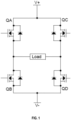
- Figure 1 illustrates an example full-bridge circuit, commonly referred to as an "H-bridge.”
- the circuit comprises four transistors, QA, QB, QC, and QD, arranged in an "H" configuration, with a load connected at the cross-bar of the "H.”
- the load may be a DC motor, for example, or an isolation transformer forming part of a power converter, for example.
- the operation of the full-bridge driver is well known, and gate driver circuits for controlling the operation of the full-bridge driver are well known and are commercially available as integrated circuits.
- a typical full-bridge circuit like that shown in Figure 1 might employ PMOS transistors on the "high side” of the full-bridge circuit, i.e., for transistors QA and QC, and NMOS transistors on the "low side.”
- the terms “high side” and “low side” simply refer to whether the transistors at issue are connected to the higher or lower voltage end of the circuit's supply voltage.
- the high-side transistors QA and QC are connected between the high-side voltage V+ and the load, while the low-side transistors QB and QD are connected between the load and the low-side voltage V-. Note that either V+ or V- might be ground, in some applications.
- high-side transistor QA and low-side transistor QD are turned on at the same time, while transistors QC and QB are switched off, so that current flows through the load in a first direction, left to right in Figure 1 .
- high-side transistor QC and QB are turned on at the same time, so that current flows through the load in the opposite direction, i.e., right to left in Figure 1 .
- Gate control circuitry connected to the gates of transistors QA, QB, QC, QD controls the timing of alternatively turning on and off these pairs of transistors, and is typically designed to provide for guard intervals between turning off one pair and turning on the other, so that, for example, transistors QA and QB are never turned on at the same time and transistors QC and QD are never turned on at the same time.
- an NMOS enhancement mode transistor When operated as switches, as they are in the full-bridge circuits discussed herein, an NMOS enhancement mode transistor is turned “on” by raising the gate-to-source voltage VGS of the transistor above a threshold voltage level, while a PMOS transistors are turned “on” by lowering the gate-to-source voltage VGS of the transistor below a threshold voltage level.
- the high-side transistors are PMOS devices and the low-side transistors are NMOS devices
- the same is true when alternately turning on high-side PMOS transistor QC and low-side NMOS transistor QB.
- Embodiments of the present invention address this problem by recouping at least some of these power losses. This is done by taking advantage of the fact that the charge discharged from the gate capacitance of the high-side PMOS device when turning that device on is at least as high, and often several times as high, as the charge that flows into the gate capacitance of the low-side NMOS device when that device is simultaneously turned on. This is because the high-side PMOS devices are often two to three times the size of the low-side NMOS devices. In a conventional circuit, the discharge current from the high-side PMOS gate is simply routed to ground (or to the low-side voltage rail).
- this discharge current is instead routed into the gate of the corresponding low-side NMOS gate.
- Charge in excess of what is needed to fully turn on the low-side NMOS transistor may be dumped to the low-side voltage rail or, in some embodiments, used to supply some other relatively small load, thereby increasing efficiency of the circuit even further.
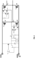
- Figure 2 illustrates a full-bridge driver circuit that employs this technique.
- the full-bridge circuit comprises high-side PMOS transistors Q1 and Q2, and low-side NMOS transistors Q3 and Q4.
- PMOS transistor Q1 and NMOS transistor Q4 are driven with complementary voltages ⁇ 1 and ⁇ 1, while PMOS transistor Q2 and NMOS transistor are alternately driven with complementary voltages ⁇ 2 and ⁇ 2.
- Output nodes Vsw1 and Vsw2 are connected to the load, which is not shown, and thus transistors Q1-Q4 form the full bridge, or H-bridge. Because transistors Q1 and Q4 are driven by voltages ⁇ 1 and ⁇ 1, they can be referred to as “the ⁇ 1 switches”; likewise, transistors Q2 and Q3 can be referred to as "the ⁇ 2 switches.”
- the circuit of Figure 2 further includes turn-on circuitry that includes switching transistors PMOS1 and NMOS1, which are coupled between the gate of high-side PMOS transistor Q3 and the gate of low-side NMOS transistor Q2, i.e., between the gates of the ⁇ 2 switches. While not shown in Figure 2 , it can be imagined that similar circuitry is connected to the ⁇ 1 switches.
- the gate of switching transistor PMOS1 When the ⁇ 2 switches are turned on during operation of the full bridge, then the gate of switching transistor PMOS1 will be lowered to a voltage that is lower than the supply voltage VDDI by the voltage of supply Vdc.
- the source of switching transistor PMOS1 will remove charge from the gate of high-side PMOS transistor Q3 until the gate of high-side PMOS transistor is discharged to a voltage Vdc-Vgs_threshold.
- the gate of switching transistor NMOS1 is raised to Vdc, and this transistor will use the charge flowing from the gate of high-side PMOS transistor Q3 to charge the gate of low-side NMOS transistor Q2.
- this quantity of charge is saved, by being routed into the gate of transistor Q2 rather than being dumped to ground.
- the gate of high-side PMOS transistor Q3 is typically larger than the gate of low-side NMOS transistor Q2, which means that more charge is pulled from the gate of transistor Q3 than is necessary to charge the gate of transistor Q2.
- this excess charge will flow through diode D1 into capacitor C1, and can be used to drive one or more loads shown in Figure 2 as "Users.” Excess charge beyond that needed to supply the "users" load is injected into the Zener diode D2. This arrangement further increases the efficiency of the driver circuit.
- circuits employing the techniques described herein may include a first PMOS high-side transistor device and a first NMOS low-side transistor device, as well as turn-on circuitry configured to turn on the first PMOS high-side transistor device while simultaneously turning on the first NMOS low-side transistor device.
- the turn-on circuitry is configured so that it turns on the first PMOS high-side transistor device and first NMOS low-side transistor device by routing charge stored in a gate of the first PMOS high-side transistor device to a gate of the first NMOS low-side transistor device, to charge the gate of the first NMOS low-side transistor device.
- the gate of the first PMOS high-side transistor device has a gate capacitance higher than a gate capacitance of the first NMOS low-side transistor device
- the circuit further comprises a capacitor coupled to the turn-on circuitry and configured to receive an excess of charge stored in the gate of the first PMOS high-side transistor device over that used to charge the gate of the first NMOS low-side transistor device, each time the first PMOS high-side transistor device and first NMOS low-side transistor device are turned on.
- This coupling may be achieved via a diode, e.g., as shown as diode D1 in Figure 2 .
- This circuit may be further configured to supply power to a load from the capacitor, in some embodiments.
- the turn-on circuitry comprises a PMOS switching transistor coupled to the gate of the first PMOS high-side transistor device, and an NMOS switching transistor coupled between the gate of the first NMOS low-side transistor device and the PMOS switching transistor.
- the turn-on circuitry in these embodiments may further comprise an arrangement of additional switching transistors configured to turn on the first PMOS high-side transistor device and NMOS low-side transistor device by lowering a gate voltage of the PMOS switching transistor to a DC voltage in between the high-side and low-side voltages while raising a gate voltage of the NMOS switching transistor to the DC voltage, so that both the PMOS switching transistor and NMOS switching transistor are conducting charge from the gate of the first PMOS high-side transistor device to the gate of the first NMOS low-side transistor device.
- the arrangement described immediately above may correspond to one high-side and low-side pair of transistors in a full-bridge configuration circuit, in some embodiments.
- the circuit described above may, in some embodiments, comprise a second PMOS high-side transistor device and a second NMOS low-side transistor device arranged so that the first PMOS high-side transistor device and second NMOS low-side transistor are operated complementarily to the first PMOS high-side transistor device and first NMOS low-side transistor.
- the circuit may further comprise additional turn-on circuitry configured to turn on the second PMOS high-side transistor device while simultaneously turning on the first NMOS low-side transistor device by routing charge stored in a gate of the second PMOS high-side transistor device to a gate of the second NMOS low-side transistor device, to charge the gate of the first NMOS low-side transistor device.
- additional turn-on circuitry may correspond to those of the turn-on circuitry described above, in some embodiments.
- the techniques described herein may also be contemplated in terms of a method for operating a circuit that comprises a first PMOS high-side transistor device and a first NMOS low-side transistor device, where the first PMOS-high side transistor device is connected between a high-side voltage and a first node of a load and the first NMOS low-side transistor device is connected between a second node of the load and a low-side voltage.
- a process flow diagram corresponding to such a method is illustrated in Figure 3 .
- the method comprises the step of turning on the first PMOS high-side transistor device while simultaneously turning on the first NMOS low-side transistor device, by routing charge stored in a gate of the first PMOS high-side transistor device to a gate of the first NMOS low-side transistor device, to charge the gate of the first NMOS low-side transistor device.
- the gate of the first PMOS high-side transistor device has a gate capacitance higher than a gate capacitance of the first NMOS low-side transistor device
- the method further comprises routing an excess of charge stored in the gate of the first PMOS high-side transistor device over that used to charge the gate of the first NMOS low-side transistor device into a capacitor coupled to turn-on circuitry, each time the first PMOS high-side transistor device and first NMOS low-side transistor device are turned on. This is shown at block 320.
- the method may further comprise supplying power to a second load from the capacitor, as shown at block 330.
- circuits described herein may be employed to improve the efficiency of various circuits, including, but not limited to, circuits employing power transistors arranged in a full-bridge configuration, such as for driving a motor or power converter.
- circuits employing power transistors arranged in a full-bridge configuration such as for driving a motor or power converter.
- the particular examples described in detail should be understood as illustrative of the inventive concepts described herein, but not limiting.
Landscapes
- Engineering & Computer Science (AREA)
- Power Engineering (AREA)
- Power Conversion In General (AREA)
- Electronic Switches (AREA)
Abstract
Description
- The present disclosure is generally related to transistor circuits and is more particularly related to full-bridge transistor power stages.
- Today, many electronic circuits, such as motor drivers and power converters, use a full-bridge topology, also referred to as an "H-bridge" topology, with PMOS and NMOS power devices. Sometimes these power devices are integrated, and sometimes not.
- Power losses in such circuits include the power losses due to the gate losses of the PMOS and NMOS power devices. This gate loss can be calculated as:

- Often the power losses due to the gate losses in full-bridge circuits can affect the system efficiency quite significantly. There are two specific cases where this occurs: at high frequency, and for large power devices. Since the design demands on systems today have the tendency to increase both switching frequency and output power capabilities, the gate losses are becoming more and more significant.
- Various embodiments of the circuits and techniques described herein address this problem by using the charge stored in the gate of the full bridge's PMOS high-side power device, which is typically much larger than the low-side NMOS power device and thus has a significantly higher gate capacitance and stored charge. Instead of simply dumping this charge into the ground when the PMOS device is turned on, this charge is used to turn on a corresponding low-side NMOS device, with the excess charge being used to provide current for other uses in the circuit.
- A circuit as defined in claim 1 and a method as defined in claim 6 are provided. The dependent claims define further embodiments.
- An example circuit comprises a first PMOS high-side transistor device and a first NMOS low-side transistor device. These devices may be part of a full-bridge (H-bridge) driver circuit in which the first PMOS high-side transistor device is connected between an input supply voltage and a first terminal of a load and the first NMOS low-side transistor device is connected between a second terminal of the load and ground. The example circuit further comprises turn-on circuitry configured to turn on the first PMOS high-side transistor device while simultaneously turning on the first NMOS low-side transistor device, by routing charge stored in a gate of the first PMOS high-side transistor device to a gate of the first NMOS low-side transistor device, to charge the gate of the first NMOS low-side transistor device.
- In some embodiments of this example circuit, the first PMOS high-side transistor device has a gate capacitance higher than a gate capacitance of the first NMOS low-side transistor device, and the circuit further comprises a capacitor coupled to the turn-on circuitry and configured to receive an excess of charge stored in the gate of the first PMOS high-side transistor device over that used to charge the gate of the first NMOS low-side transistor device, each time the first PMOS high-side transistor device and first NMOS low-side transistor device are turned on. This capacitor may, in some embodiments, be configured to supply current to a different load from that of the full-bridge driver circuit.
- In some embodiments of the example circuit, the turn-on circuitry comprises a PMOS switching transistor coupled to the gate of the first PMOS high-side transistor device and an NMOS switching transistor coupled between the gate of the first NMOS low-side transistor device and the PMOS switching transistor, as well as an arrangement of additional switching transistors configured to turn on the first PMOS high-side transistor device and NMOS low-side transistor device by lowering a gate voltage of the PMOS switching transistor to a DC voltage in between the high-side and low-side voltages while raising a gate voltage of the NMOS switching transistor to the DC voltage, so that both the PMOS switching transistor and the NMOS switching transistor are conducting charge from the gate of the first PMOS high-side transistor device to the gate of the first NMOS low-side transistor device.
-
-
Figure 1 illustrates an example full-bridge circuit. -
Figure 2 illustrates an example full-bridge circuit including turn-on circuitry, according to some embodiments. -
Figure 3 is a process flow diagram illustrating an example method, according to some embodiments. - Examples of the inventive techniques and circuits will be described in detail below, with reference to the attached figures.
- In the description that follows, the terminology "connected to" or "connected between" generally means that one node is electrically connected to another, where this connection is via a low-resistance connection unless the context clearly indicates otherwise. The terminology "coupled to," as used herein, means that one node of a circuit is connected to another, either directly (through a low-resistance connection) or through an intervening component, in such a way that current flows, at least some of the time, from one node to the other. Thus, one node might be coupled to another through a switching transistor, a diode, or a resistor, in various examples.
-
Figure 1 illustrates an example full-bridge circuit, commonly referred to as an "H-bridge." The circuit comprises four transistors, QA, QB, QC, and QD, arranged in an "H" configuration, with a load connected at the cross-bar of the "H." The load may be a DC motor, for example, or an isolation transformer forming part of a power converter, for example. The operation of the full-bridge driver is well known, and gate driver circuits for controlling the operation of the full-bridge driver are well known and are commercially available as integrated circuits. - In high-power applications in particular, a typical full-bridge circuit like that shown in
Figure 1 might employ PMOS transistors on the "high side" of the full-bridge circuit, i.e., for transistors QA and QC, and NMOS transistors on the "low side." The terms "high side" and "low side" simply refer to whether the transistors at issue are connected to the higher or lower voltage end of the circuit's supply voltage. In the example illustrated inFigure 1 , the high-side transistors QA and QC are connected between the high-side voltage V+ and the load, while the low-side transistors QB and QD are connected between the load and the low-side voltage V-. Note that either V+ or V- might be ground, in some applications. - During operation of the full-bridge circuit, high-side transistor QA and low-side transistor QD are turned on at the same time, while transistors QC and QB are switched off, so that current flows through the load in a first direction, left to right in
Figure 1 . Alternately, high-side transistor QC and QB are turned on at the same time, so that current flows through the load in the opposite direction, i.e., right to left inFigure 1 . Gate control circuitry connected to the gates of transistors QA, QB, QC, QD controls the timing of alternatively turning on and off these pairs of transistors, and is typically designed to provide for guard intervals between turning off one pair and turning on the other, so that, for example, transistors QA and QB are never turned on at the same time and transistors QC and QD are never turned on at the same time. - When operated as switches, as they are in the full-bridge circuits discussed herein, an NMOS enhancement mode transistor is turned "on" by raising the gate-to-source voltage VGS of the transistor above a threshold voltage level, while a PMOS transistors are turned "on" by lowering the gate-to-source voltage VGS of the transistor below a threshold voltage level. Thus, in a configuration where the high-side transistors are PMOS devices and the low-side transistors are NMOS devices, this means that turning on the low-side NMOS transistor QD involves charging the intrinsic gate capacitance of the NMOS transistor QD, while simultaneously turning on high-side PMOS transistor QA involves discharging the intrinsic gate capacitance of PMOS transistor QA. The same is true when alternately turning on high-side PMOS transistor QC and low-side NMOS transistor QB.
- As briefly noted above, this charging and discharging of the gate capacitances during operation of the full-bridge circuit causes power losses that increase with both the switching frequency and the intrinsic gate capacitances of the devices. In high-frequency power applications, these power losses can be significant.
- Embodiments of the present invention address this problem by recouping at least some of these power losses. This is done by taking advantage of the fact that the charge discharged from the gate capacitance of the high-side PMOS device when turning that device on is at least as high, and often several times as high, as the charge that flows into the gate capacitance of the low-side NMOS device when that device is simultaneously turned on. This is because the high-side PMOS devices are often two to three times the size of the low-side NMOS devices. In a conventional circuit, the discharge current from the high-side PMOS gate is simply routed to ground (or to the low-side voltage rail). In the circuits described herein, a portion of this discharge current is instead routed into the gate of the corresponding low-side NMOS gate. Charge in excess of what is needed to fully turn on the low-side NMOS transistor may be dumped to the low-side voltage rail or, in some embodiments, used to supply some other relatively small load, thereby increasing efficiency of the circuit even further.
-
Figure 2 illustrates a full-bridge driver circuit that employs this technique. Here, the full-bridge circuit comprises high-side PMOS transistors Q1 and Q2, and low-side NMOS transistors Q3 and Q4. PMOS transistor Q1 and NMOS transistor Q4 are driven with complementary voltages Φ1 and Φ1, while PMOS transistor Q2 and NMOS transistor are alternately driven with complementary voltages Φ2 and Φ2. Output nodes Vsw1 and Vsw2 are connected to the load, which is not shown, and thus transistors Q1-Q4 form the full bridge, or H-bridge. Because transistors Q1 and Q4 are driven by voltages Φ1 and Φ1, they can be referred to as "the Φ1 switches"; likewise, transistors Q2 and Q3 can be referred to as "the Φ2 switches." - The circuit of
Figure 2 further includes turn-on circuitry that includes switching transistors PMOS1 and NMOS1, which are coupled between the gate of high-side PMOS transistor Q3 and the gate of low-side NMOS transistor Q2, i.e., between the gates of the Φ2 switches. While not shown inFigure 2 , it can be imagined that similar circuitry is connected to the Φ1 switches. - When the Φ2 switches are turned on during operation of the full bridge, then the gate of switching transistor PMOS1 will be lowered to a voltage that is lower than the supply voltage VDDI by the voltage of supply Vdc. The source of switching transistor PMOS1 will remove charge from the gate of high-side PMOS transistor Q3 until the gate of high-side PMOS transistor is discharged to a voltage Vdc-Vgs_threshold. At the same time, the gate of switching transistor NMOS1 is raised to Vdc, and this transistor will use the charge flowing from the gate of high-side PMOS transistor Q3 to charge the gate of low-side NMOS transistor Q2. Thus, this quantity of charge is saved, by being routed into the gate of transistor Q2 rather than being dumped to ground.
- However, the gate of high-side PMOS transistor Q3 is typically larger than the gate of low-side NMOS transistor Q2, which means that more charge is pulled from the gate of transistor Q3 than is necessary to charge the gate of transistor Q2. With the circuit arrangement shown in
Figure 2 , this excess charge will flow through diode D1 into capacitor C1, and can be used to drive one or more loads shown inFigure 2 as "Users." Excess charge beyond that needed to supply the "users" load is injected into the Zener diode D2. This arrangement further increases the efficiency of the driver circuit. - While not shown in
Figure 2 , it will be appreciated that similar turn-on circuitry can be connected to the Φ1 switches. Excess charge pulled from the gate of transistor Q1 beyond that needed to charge the gate of transistor Q4 can similarly be routed to capacitor C1 and load "users," through another diode. - In view of the detailed explanation of
Figure 2 provided above, it will be appreciated that circuits employing the techniques described herein may include a first PMOS high-side transistor device and a first NMOS low-side transistor device, as well as turn-on circuitry configured to turn on the first PMOS high-side transistor device while simultaneously turning on the first NMOS low-side transistor device. The turn-on circuitry is configured so that it turns on the first PMOS high-side transistor device and first NMOS low-side transistor device by routing charge stored in a gate of the first PMOS high-side transistor device to a gate of the first NMOS low-side transistor device, to charge the gate of the first NMOS low-side transistor device. - In some embodiments, the gate of the first PMOS high-side transistor device has a gate capacitance higher than a gate capacitance of the first NMOS low-side transistor device, and the circuit further comprises a capacitor coupled to the turn-on circuitry and configured to receive an excess of charge stored in the gate of the first PMOS high-side transistor device over that used to charge the gate of the first NMOS low-side transistor device, each time the first PMOS high-side transistor device and first NMOS low-side transistor device are turned on. This coupling may be achieved via a diode, e.g., as shown as diode D1 in
Figure 2 . This circuit may be further configured to supply power to a load from the capacitor, in some embodiments. - In some embodiments, the turn-on circuitry comprises a PMOS switching transistor coupled to the gate of the first PMOS high-side transistor device, and an NMOS switching transistor coupled between the gate of the first NMOS low-side transistor device and the PMOS switching transistor. The turn-on circuitry in these embodiments may further comprise an arrangement of additional switching transistors configured to turn on the first PMOS high-side transistor device and NMOS low-side transistor device by lowering a gate voltage of the PMOS switching transistor to a DC voltage in between the high-side and low-side voltages while raising a gate voltage of the NMOS switching transistor to the DC voltage, so that both the PMOS switching transistor and NMOS switching transistor are conducting charge from the gate of the first PMOS high-side transistor device to the gate of the first NMOS low-side transistor device.
- The arrangement described immediately above may correspond to one high-side and low-side pair of transistors in a full-bridge configuration circuit, in some embodiments. Thus, the circuit described above may, in some embodiments, comprise a second PMOS high-side transistor device and a second NMOS low-side transistor device arranged so that the first PMOS high-side transistor device and second NMOS low-side transistor are operated complementarily to the first PMOS high-side transistor device and first NMOS low-side transistor. In these embodiments, the circuit may further comprise additional turn-on circuitry configured to turn on the second PMOS high-side transistor device while simultaneously turning on the first NMOS low-side transistor device by routing charge stored in a gate of the second PMOS high-side transistor device to a gate of the second NMOS low-side transistor device, to charge the gate of the first NMOS low-side transistor device. The details of this additional turn-on circuitry may correspond to those of the turn-on circuitry described above, in some embodiments.
- The techniques described herein may also be contemplated in terms of a method for operating a circuit that comprises a first PMOS high-side transistor device and a first NMOS low-side transistor device, where the first PMOS-high side transistor device is connected between a high-side voltage and a first node of a load and the first NMOS low-side transistor device is connected between a second node of the load and a low-side voltage. A process flow diagram corresponding to such a method is illustrated in
Figure 3 . - As shown at block 310, the method comprises the step of turning on the first PMOS high-side transistor device while simultaneously turning on the first NMOS low-side transistor device, by routing charge stored in a gate of the first PMOS high-side transistor device to a gate of the first NMOS low-side transistor device, to charge the gate of the first NMOS low-side transistor device. In some embodiments, the gate of the first PMOS high-side transistor device has a gate capacitance higher than a gate capacitance of the first NMOS low-side transistor device, and the method further comprises routing an excess of charge stored in the gate of the first PMOS high-side transistor device over that used to charge the gate of the first NMOS low-side transistor device into a capacitor coupled to turn-on circuitry, each time the first PMOS high-side transistor device and first NMOS low-side transistor device are turned on. This is shown at
block 320. The method may further comprise supplying power to a second load from the capacitor, as shown atblock 330. - The techniques and circuits described herein may be employed to improve the efficiency of various circuits, including, but not limited to, circuits employing power transistors arranged in a full-bridge configuration, such as for driving a motor or power converter. The particular examples described in detail should be understood as illustrative of the inventive concepts described herein, but not limiting.
Claims (9)
- A circuit, comprising:a first PMOS high-side transistor device;a first NMOS low-side transistor device; andturn-on circuitry configured to turn on the first PMOS high-side transistor device while simultaneously turning on the first NMOS low-side transistor device, by routing charge stored in a gate of the first PMOS high-side transistor device to a gate of the first NMOS low-side transistor device, to charge the gate of the first NMOS low-side transistor device.
- The circuit of claim 1, wherein the gate of the first PMOS high-side transistor device has a gate capacitance higher than a gate capacitance of the first NMOS low-side transistor device, and wherein the circuit further comprises a capacitor coupled to the turn-on circuitry and configured to receive an excess of charge stored in the gate of the first PMOS high-side transistor device over that used to charge the gate of the first NMOS low-side transistor device, each time the first PMOS high-side transistor device and first NMOS low-side transistor device are turned on.
- The circuit of claim 2, wherein the circuit is further configured to supply power to a load from the capacitor.
- The circuit of any one of claims 1 to 3, wherein the turn-on circuitry comprises:a PMOS switching transistor coupled to the gate of the first PMOS high-side transistor device;an NMOS switching transistor coupled between the gate of the first NMOS low-side transistor device and the PMOS switching transistor; andan arrangement of additional switching transistors configured to turn on the first PMOS high-side transistor device and NMOS low-side transistor device by lowering a gate voltage of the PMOS switching transistor to a DC voltage in between the high-side and low-side voltages while raising a gate voltage of the NMOS switching transistor to the DC voltage, so that both the PMOS switching transistor and NMOS switching transistor are conducting charge from the gate of the first PMOS high-side transistor device to the gate of the first NMOS low-side transistor device.
- The circuit of any one of claims 1 to 4 wherein the circuit is a full-bridge circuit comprising a second PMOS high-side transistor device and a second NMOS low-side transistor device arranged so that the first PMOS high- side transistor device and second NMOS low-side transistor are operated complementarily to the first PMOS high-side transistor device and first NMOS low-side transistor, and further comprising additional turn-on circuitry configured to turn on the second PMOS high-side transistor device while simultaneously turning on the first NMOS low-side transistor device by routing charge stored in a gate of the second PMOS high-side transistor device to a gate of the second NMOS low-side transistor device, to charge the gate of the first NMOS low-side transistor device.
- A method for operating a circuit comprising a PMOS high-side transistor device and a NMOS low-side transistor device, wherein the PMOS-high side transistor device is connected between a high-side voltage and a first node of a load and the NMOS low-side transistor device is connected between a second node of the load and a low-side voltage, the method comprising:
turning on the PMOS high-side transistor device while simultaneously on the NMOS low-side transistor device, by routing charge stored in a gate of the first PMOS high-side transistor device to a gate of the NMOS low-side transistor device, to charge the gate of the NMOS low-side transistor device. - The method of claim 6, wherein the gate of the PMOS high-side transistor device has a gate capacitance higher than a gate capacitance of the NMOS low-side transistor device, and wherein the method further comprises routing an excess of charge stored in the gate of the PMOS high-side transistor device over that used to charge the gate of the NMOS low-side transistor device into a capacitor coupled to turn-on circuitry, each time the PMOS high-side transistor device and NMOS low-side transistor device are turned on.
- The method of claim 7, wherein the method further comprises supplying power to a second load from the capacitor.
- The method of any one of claims 6 to 8, wherein the method operates the circuit of any one of claims 1 to 5.
Applications Claiming Priority (1)
| Application Number | Priority Date | Filing Date | Title |
|---|---|---|---|
| US17/707,365 US11777497B1 (en) | 2022-03-29 | 2022-03-29 | Efficiency concept for driving a PMOS and NMOS full-bridge power stage |
Publications (2)
| Publication Number | Publication Date |
|---|---|
| EP4254795A1 true EP4254795A1 (en) | 2023-10-04 |
| EP4254795B1 EP4254795B1 (en) | 2025-07-23 |
Family
ID=85778782
Family Applications (1)
| Application Number | Title | Priority Date | Filing Date |
|---|---|---|---|
| EP23164663.9A Active EP4254795B1 (en) | 2022-03-29 | 2023-03-28 | Efficient concept for driving a pmos and nmos full-bridge power stage |
Country Status (3)
| Country | Link |
|---|---|
| US (1) | US11777497B1 (en) |
| EP (1) | EP4254795B1 (en) |
| CN (1) | CN116896256A (en) |
Citations (2)
| Publication number | Priority date | Publication date | Assignee | Title |
|---|---|---|---|---|
| JPH053626A (en) * | 1991-06-27 | 1993-01-08 | Toyota Motor Corp | Electronic controller installed on car |
| US10972095B2 (en) * | 2019-07-02 | 2021-04-06 | Research & Business Foundation Sungkyunkwan University | Pulse width modulation buck converter |
Family Cites Families (3)
| Publication number | Priority date | Publication date | Assignee | Title |
|---|---|---|---|---|
| US7746153B1 (en) * | 2007-11-09 | 2010-06-29 | National Semiconductor Corporation | Power FET gate charge recovery |
| US10256812B2 (en) * | 2016-07-08 | 2019-04-09 | Infineon Technologies Austria Ag | Half bridge coupled resonant gate drivers |
| US10931277B2 (en) * | 2019-03-04 | 2021-02-23 | Texas Instruments Incorporated | Power transistor gate-charge harvester for internal supply generation |
-
2022
- 2022-03-29 US US17/707,365 patent/US11777497B1/en active Active
-
2023
- 2023-03-28 CN CN202310310755.0A patent/CN116896256A/en active Pending
- 2023-03-28 EP EP23164663.9A patent/EP4254795B1/en active Active
Patent Citations (2)
| Publication number | Priority date | Publication date | Assignee | Title |
|---|---|---|---|---|
| JPH053626A (en) * | 1991-06-27 | 1993-01-08 | Toyota Motor Corp | Electronic controller installed on car |
| US10972095B2 (en) * | 2019-07-02 | 2021-04-06 | Research & Business Foundation Sungkyunkwan University | Pulse width modulation buck converter |
Also Published As
| Publication number | Publication date |
|---|---|
| US11777497B1 (en) | 2023-10-03 |
| EP4254795B1 (en) | 2025-07-23 |
| CN116896256A (en) | 2023-10-17 |
Similar Documents
| Publication | Publication Date | Title |
|---|---|---|
| US5963066A (en) | Semiconductor device which drives low-voltage driven switching device, using low-voltage direct current power source, a diode and a capacitor | |
| KR101385065B1 (en) | Charge pump circuit and method therefor | |
| JP4113436B2 (en) | Gate drive device | |
| US11543846B2 (en) | Gate driver circuit for reducing deadtime inefficiencies | |
| CN113630112B (en) | Circuit for transmitting signals between different voltage domains and corresponding method for transmitting signals | |
| EP3907888A1 (en) | A circuit to transfer a signal between different voltage domains and corresponding method to transfer a signal | |
| EP1696565B1 (en) | Inverter apparatus with improved gate drive for power mosfet | |
| CN106233629A (en) | Electric charge recycling circuit including the switch power level with floating rail | |
| CN116868496B (en) | Control device and control method for power conversion device | |
| EP2073385B1 (en) | Semiconductor output circuit for controlling power supply to a load | |
| US20080309307A1 (en) | High Voltage Power Switches Using Low Voltage Transistors | |
| EP2073386B1 (en) | Semiconductor output circuit | |
| JP2021010258A (en) | Gate driver, switching circuit, motor driver, and controller of dc/dc converter | |
| EP2639956A1 (en) | Driver circuit and inverter circuit | |
| CN117277806A (en) | Driving circuit and switching power supply circuit | |
| JP2006203987A (en) | Switching regulator circuit | |
| EP4254795B1 (en) | Efficient concept for driving a pmos and nmos full-bridge power stage | |
| KR20190108785A (en) | Power source converter, apparatus for driving switching element and apparatus for driving load | |
| JP4319336B2 (en) | MOS switching circuit | |
| US8638129B2 (en) | Power circuit | |
| US6150854A (en) | Circuit arrangement for switching an inductive load | |
| JP4151163B2 (en) | MOS transistor drive circuit | |
| JP4888199B2 (en) | Load drive device | |
| JP4658770B2 (en) | Semiconductor device | |
| JP3681731B2 (en) | Drive circuit |
Legal Events
| Date | Code | Title | Description |
|---|---|---|---|
| PUAI | Public reference made under article 153(3) epc to a published international application that has entered the european phase |
Free format text: ORIGINAL CODE: 0009012 |
|
| STAA | Information on the status of an ep patent application or granted ep patent |
Free format text: STATUS: THE APPLICATION HAS BEEN PUBLISHED |
|
| AK | Designated contracting states |
Kind code of ref document: A1 Designated state(s): AL AT BE BG CH CY CZ DE DK EE ES FI FR GB GR HR HU IE IS IT LI LT LU LV MC ME MK MT NL NO PL PT RO RS SE SI SK SM TR |
|
| STAA | Information on the status of an ep patent application or granted ep patent |
Free format text: STATUS: REQUEST FOR EXAMINATION WAS MADE |
|
| 17P | Request for examination filed |
Effective date: 20240312 |
|
| RBV | Designated contracting states (corrected) |
Designated state(s): AL AT BE BG CH CY CZ DE DK EE ES FI FR GB GR HR HU IE IS IT LI LT LU LV MC ME MK MT NL NO PL PT RO RS SE SI SK SM TR |
|
| GRAP | Despatch of communication of intention to grant a patent |
Free format text: ORIGINAL CODE: EPIDOSNIGR1 |
|
| STAA | Information on the status of an ep patent application or granted ep patent |
Free format text: STATUS: GRANT OF PATENT IS INTENDED |
|
| RIC1 | Information provided on ipc code assigned before grant |
Ipc: H03K 17/687 20060101ALI20250210BHEP Ipc: H02M 7/5387 20070101ALI20250210BHEP Ipc: H02M 1/08 20060101ALI20250210BHEP Ipc: H02M 1/00 20060101ALI20250210BHEP Ipc: H03K 17/06 20060101AFI20250210BHEP |
|
| INTG | Intention to grant announced |
Effective date: 20250312 |
|
| GRAS | Grant fee paid |
Free format text: ORIGINAL CODE: EPIDOSNIGR3 |
|
| GRAA | (expected) grant |
Free format text: ORIGINAL CODE: 0009210 |
|
| STAA | Information on the status of an ep patent application or granted ep patent |
Free format text: STATUS: THE PATENT HAS BEEN GRANTED |
|
| P01 | Opt-out of the competence of the unified patent court (upc) registered |
Free format text: CASE NUMBER: APP_25505/2025 Effective date: 20250528 |
|
| AK | Designated contracting states |
Kind code of ref document: B1 Designated state(s): AL AT BE BG CH CY CZ DE DK EE ES FI FR GB GR HR HU IE IS IT LI LT LU LV MC ME MK MT NL NO PL PT RO RS SE SI SK SM TR |
|
| REG | Reference to a national code |
Ref country code: GB Ref legal event code: FG4D |
|
| REG | Reference to a national code |
Ref country code: CH Ref legal event code: EP |
|
| REG | Reference to a national code |
Ref country code: IE Ref legal event code: FG4D |
|
| REG | Reference to a national code |
Ref country code: DE Ref legal event code: R096 Ref document number: 602023004939 Country of ref document: DE |
|
| REG | Reference to a national code |
Ref country code: SE Ref legal event code: TRGR |
|
| REG | Reference to a national code |
Ref country code: NL Ref legal event code: MP Effective date: 20250723 |
|
| PG25 | Lapsed in a contracting state [announced via postgrant information from national office to epo] |
Ref country code: PT Free format text: LAPSE BECAUSE OF FAILURE TO SUBMIT A TRANSLATION OF THE DESCRIPTION OR TO PAY THE FEE WITHIN THE PRESCRIBED TIME-LIMIT Effective date: 20251124 |
|
| PG25 | Lapsed in a contracting state [announced via postgrant information from national office to epo] |
Ref country code: NL Free format text: LAPSE BECAUSE OF FAILURE TO SUBMIT A TRANSLATION OF THE DESCRIPTION OR TO PAY THE FEE WITHIN THE PRESCRIBED TIME-LIMIT Effective date: 20250723 |
|
| REG | Reference to a national code |
Ref country code: AT Ref legal event code: MK05 Ref document number: 1817511 Country of ref document: AT Kind code of ref document: T Effective date: 20250723 |
|
| PG25 | Lapsed in a contracting state [announced via postgrant information from national office to epo] |
Ref country code: IS Free format text: LAPSE BECAUSE OF FAILURE TO SUBMIT A TRANSLATION OF THE DESCRIPTION OR TO PAY THE FEE WITHIN THE PRESCRIBED TIME-LIMIT Effective date: 20251123 |
|
| PG25 | Lapsed in a contracting state [announced via postgrant information from national office to epo] |
Ref country code: NO Free format text: LAPSE BECAUSE OF FAILURE TO SUBMIT A TRANSLATION OF THE DESCRIPTION OR TO PAY THE FEE WITHIN THE PRESCRIBED TIME-LIMIT Effective date: 20251023 |
|
| REG | Reference to a national code |
Ref country code: LT Ref legal event code: MG9D |
|
| PG25 | Lapsed in a contracting state [announced via postgrant information from national office to epo] |
Ref country code: AT Free format text: LAPSE BECAUSE OF FAILURE TO SUBMIT A TRANSLATION OF THE DESCRIPTION OR TO PAY THE FEE WITHIN THE PRESCRIBED TIME-LIMIT Effective date: 20250723 |
|
| PG25 | Lapsed in a contracting state [announced via postgrant information from national office to epo] |
Ref country code: FI Free format text: LAPSE BECAUSE OF FAILURE TO SUBMIT A TRANSLATION OF THE DESCRIPTION OR TO PAY THE FEE WITHIN THE PRESCRIBED TIME-LIMIT Effective date: 20250723 |
|
| PG25 | Lapsed in a contracting state [announced via postgrant information from national office to epo] |
Ref country code: HR Free format text: LAPSE BECAUSE OF FAILURE TO SUBMIT A TRANSLATION OF THE DESCRIPTION OR TO PAY THE FEE WITHIN THE PRESCRIBED TIME-LIMIT Effective date: 20250723 |
|
| PG25 | Lapsed in a contracting state [announced via postgrant information from national office to epo] |
Ref country code: GR Free format text: LAPSE BECAUSE OF FAILURE TO SUBMIT A TRANSLATION OF THE DESCRIPTION OR TO PAY THE FEE WITHIN THE PRESCRIBED TIME-LIMIT Effective date: 20251024 |
|
| PG25 | Lapsed in a contracting state [announced via postgrant information from national office to epo] |
Ref country code: LV Free format text: LAPSE BECAUSE OF FAILURE TO SUBMIT A TRANSLATION OF THE DESCRIPTION OR TO PAY THE FEE WITHIN THE PRESCRIBED TIME-LIMIT Effective date: 20250723 |
|
| PG25 | Lapsed in a contracting state [announced via postgrant information from national office to epo] |
Ref country code: BG Free format text: LAPSE BECAUSE OF FAILURE TO SUBMIT A TRANSLATION OF THE DESCRIPTION OR TO PAY THE FEE WITHIN THE PRESCRIBED TIME-LIMIT Effective date: 20250723 Ref country code: PL Free format text: LAPSE BECAUSE OF FAILURE TO SUBMIT A TRANSLATION OF THE DESCRIPTION OR TO PAY THE FEE WITHIN THE PRESCRIBED TIME-LIMIT Effective date: 20250723 |
|
| PG25 | Lapsed in a contracting state [announced via postgrant information from national office to epo] |
Ref country code: RS Free format text: LAPSE BECAUSE OF FAILURE TO SUBMIT A TRANSLATION OF THE DESCRIPTION OR TO PAY THE FEE WITHIN THE PRESCRIBED TIME-LIMIT Effective date: 20251023 |
|
| PG25 | Lapsed in a contracting state [announced via postgrant information from national office to epo] |
Ref country code: ES Free format text: LAPSE BECAUSE OF FAILURE TO SUBMIT A TRANSLATION OF THE DESCRIPTION OR TO PAY THE FEE WITHIN THE PRESCRIBED TIME-LIMIT Effective date: 20250723 |
|
| PG25 | Lapsed in a contracting state [announced via postgrant information from national office to epo] |
Ref country code: SM Free format text: LAPSE BECAUSE OF FAILURE TO SUBMIT A TRANSLATION OF THE DESCRIPTION OR TO PAY THE FEE WITHIN THE PRESCRIBED TIME-LIMIT Effective date: 20250723 |
|
| PGFP | Annual fee paid to national office [announced via postgrant information from national office to epo] |
Ref country code: SE Payment date: 20260319 Year of fee payment: 4 |
|
| PG25 | Lapsed in a contracting state [announced via postgrant information from national office to epo] |
Ref country code: DK Free format text: LAPSE BECAUSE OF FAILURE TO SUBMIT A TRANSLATION OF THE DESCRIPTION OR TO PAY THE FEE WITHIN THE PRESCRIBED TIME-LIMIT Effective date: 20250723 |
|
| PG25 | Lapsed in a contracting state [announced via postgrant information from national office to epo] |
Ref country code: IT Free format text: LAPSE BECAUSE OF FAILURE TO SUBMIT A TRANSLATION OF THE DESCRIPTION OR TO PAY THE FEE WITHIN THE PRESCRIBED TIME-LIMIT Effective date: 20250723 |
|
| PG25 | Lapsed in a contracting state [announced via postgrant information from national office to epo] |
Ref country code: CZ Free format text: LAPSE BECAUSE OF FAILURE TO SUBMIT A TRANSLATION OF THE DESCRIPTION OR TO PAY THE FEE WITHIN THE PRESCRIBED TIME-LIMIT Effective date: 20250723 |
|
| REG | Reference to a national code |
Ref country code: DE Ref legal event code: R097 Ref document number: 602023004939 Country of ref document: DE |
|
| PG25 | Lapsed in a contracting state [announced via postgrant information from national office to epo] |
Ref country code: SK Free format text: LAPSE BECAUSE OF FAILURE TO SUBMIT A TRANSLATION OF THE DESCRIPTION OR TO PAY THE FEE WITHIN THE PRESCRIBED TIME-LIMIT Effective date: 20250723 Ref country code: EE Free format text: LAPSE BECAUSE OF FAILURE TO SUBMIT A TRANSLATION OF THE DESCRIPTION OR TO PAY THE FEE WITHIN THE PRESCRIBED TIME-LIMIT Effective date: 20250723 |
|
| PLBE | No opposition filed within time limit |
Free format text: ORIGINAL CODE: 0009261 |
|
| STAA | Information on the status of an ep patent application or granted ep patent |
Free format text: STATUS: NO OPPOSITION FILED WITHIN TIME LIMIT |
|
| REG | Reference to a national code |
Ref country code: CH Ref legal event code: L10 Free format text: ST27 STATUS EVENT CODE: U-0-0-L10-L00 (AS PROVIDED BY THE NATIONAL OFFICE) Effective date: 20260604 |
|
| PG25 | Lapsed in a contracting state [announced via postgrant information from national office to epo] |
Ref country code: LT Free format text: LAPSE BECAUSE OF FAILURE TO SUBMIT A TRANSLATION OF THE DESCRIPTION OR TO PAY THE FEE WITHIN THE PRESCRIBED TIME-LIMIT Effective date: 20250723 |
|
| 26N | No opposition filed |
Effective date: 20260424 |
|
| PGFP | Annual fee paid to national office [announced via postgrant information from national office to epo] |
Ref country code: DE Payment date: 20260520 Year of fee payment: 4 |