EP4254666A1 - Antenna structure - Google Patents
Antenna structure Download PDFInfo
- Publication number
- EP4254666A1 EP4254666A1 EP21897858.3A EP21897858A EP4254666A1 EP 4254666 A1 EP4254666 A1 EP 4254666A1 EP 21897858 A EP21897858 A EP 21897858A EP 4254666 A1 EP4254666 A1 EP 4254666A1
- Authority
- EP
- European Patent Office
- Prior art keywords
- annular pattern
- antenna
- substrate
- grounding
- antenna structure
- Prior art date
- Legal status (The legal status is an assumption and is not a legal conclusion. Google has not performed a legal analysis and makes no representation as to the accuracy of the status listed.)
- Withdrawn
Links
Images




Classifications
-
- H—ELECTRICITY
- H01—ELECTRIC ELEMENTS
- H01Q—ANTENNAS, i.e. RADIO AERIALS
- H01Q1/00—Details of, or arrangements associated with, antennas
- H01Q1/12—Supports; Mounting means
- H01Q1/22—Supports; Mounting means by structural association with other equipment or articles
- H01Q1/2283—Supports; Mounting means by structural association with other equipment or articles mounted in or on the surface of a semiconductor substrate as a chip-type antenna or integrated with other components into an IC package
-
- H—ELECTRICITY
- H01—ELECTRIC ELEMENTS
- H01Q—ANTENNAS, i.e. RADIO AERIALS
- H01Q19/00—Combinations of primary active antenna elements and units with secondary devices, e.g. with quasi-optical devices, for giving the antenna a desired directional characteristic
- H01Q19/06—Combinations of primary active antenna elements and units with secondary devices, e.g. with quasi-optical devices, for giving the antenna a desired directional characteristic using refracting or diffracting devices, e.g. lens
-
- H—ELECTRICITY
- H01—ELECTRIC ELEMENTS
- H01Q—ANTENNAS, i.e. RADIO AERIALS
- H01Q1/00—Details of, or arrangements associated with, antennas
- H01Q1/36—Structural form of radiating elements, e.g. cone, spiral, umbrella; Particular materials used therewith
- H01Q1/38—Structural form of radiating elements, e.g. cone, spiral, umbrella; Particular materials used therewith formed by a conductive layer on an insulating support
-
- H—ELECTRICITY
- H01—ELECTRIC ELEMENTS
- H01Q—ANTENNAS, i.e. RADIO AERIALS
- H01Q1/00—Details of, or arrangements associated with, antennas
- H01Q1/48—Earthing means; Earth screens; Counterpoises
-
- H—ELECTRICITY
- H01—ELECTRIC ELEMENTS
- H01Q—ANTENNAS, i.e. RADIO AERIALS
- H01Q15/00—Devices for reflection, refraction, diffraction or polarisation of waves radiated from an antenna, e.g. quasi-optical devices
- H01Q15/0006—Devices acting selectively as reflecting surface, as diffracting or as refracting device, e.g. frequency filtering or angular spatial filtering devices
- H01Q15/0053—Selective devices used as spatial filter or angular sidelobe filter
-
- H—ELECTRICITY
- H01—ELECTRIC ELEMENTS
- H01Q—ANTENNAS, i.e. RADIO AERIALS
- H01Q19/00—Combinations of primary active antenna elements and units with secondary devices, e.g. with quasi-optical devices, for giving the antenna a desired directional characteristic
- H01Q19/02—Details
- H01Q19/021—Means for reducing undesirable effects
-
- H—ELECTRICITY
- H01—ELECTRIC ELEMENTS
- H01Q—ANTENNAS, i.e. RADIO AERIALS
- H01Q21/00—Antenna arrays or systems
- H01Q21/06—Arrays of individually energised antenna units similarly polarised and spaced apart
- H01Q21/061—Two dimensional planar arrays
- H01Q21/065—Patch antenna array
-
- H—ELECTRICITY
- H01—ELECTRIC ELEMENTS
- H01Q—ANTENNAS, i.e. RADIO AERIALS
- H01Q21/00—Antenna arrays or systems
- H01Q21/24—Combinations of antenna units polarised in different directions for transmitting or receiving circularly and elliptically polarised waves or waves linearly polarised in any direction
-
- H—ELECTRICITY
- H01—ELECTRIC ELEMENTS
- H01Q—ANTENNAS, i.e. RADIO AERIALS
- H01Q9/00—Electrically-short antennas having dimensions not more than twice the operating wavelength and consisting of conductive active radiating elements
- H01Q9/04—Resonant antennas
- H01Q9/0407—Substantially flat resonant element parallel to ground plane, e.g. patch antenna
- H01Q9/0414—Substantially flat resonant element parallel to ground plane, e.g. patch antenna in a stacked or folded configuration
-
- H—ELECTRICITY
- H01—ELECTRIC ELEMENTS
- H01Q—ANTENNAS, i.e. RADIO AERIALS
- H01Q9/00—Electrically-short antennas having dimensions not more than twice the operating wavelength and consisting of conductive active radiating elements
- H01Q9/04—Resonant antennas
- H01Q9/0407—Substantially flat resonant element parallel to ground plane, e.g. patch antenna
- H01Q9/045—Substantially flat resonant element parallel to ground plane, e.g. patch antenna with particular feeding means
- H01Q9/0457—Substantially flat resonant element parallel to ground plane, e.g. patch antenna with particular feeding means electromagnetically coupled to the feed line
-
- H—ELECTRICITY
- H01—ELECTRIC ELEMENTS
- H01Q—ANTENNAS, i.e. RADIO AERIALS
- H01Q9/00—Electrically-short antennas having dimensions not more than twice the operating wavelength and consisting of conductive active radiating elements
- H01Q9/04—Resonant antennas
- H01Q9/0407—Substantially flat resonant element parallel to ground plane, e.g. patch antenna
- H01Q9/0464—Annular ring patch
Definitions
- the present invention relates to an antenna structure.
- a communication device that uses a wireless network includes an antenna structure as described in Patent Document 1, for example, for transmission and reception of electrical signals.
- Such an antenna structure has, for example, a structure in which an electric filter substrate is layered on an upper surface of a control substrate (RF control substrate) and an antenna substrate is layered on an upper surface of the electric filter substrate.
- the antenna substrate and the control substrate are connected via the electric filter substrate. This results in longer wiring lines and a higher transmission loss.
- each of the antenna substrate, the electric filter substrate, and the control substrate cannot be reused. As a result, the yield is lowered. In order to avoid such defects, a relatively expensive low-dielectric material or low-loss material is employed, which leads to an increase in cost.
- the antenna substrate, the electric filter substrate, and the control substrate have substantially the same size in a plan view. Since such an antenna structure has the layered structure, each member cannot be applied with an arbitrary size according to an arrangement location. As a result, it is difficult to miniaturize the antenna structure.
- Patent Document 1 JP 6-152101 A
- An antenna structure includes an antenna substrate including a first surface and a second surface located on an opposite side to the first surface, a transmissive filter located over the first surface, and a control substrate located on the second surface.
- the transmissive filter includes a first annular pattern located on a surface facing the first surface, and a second annular pattern located on a surface on an opposite side to the surface facing the first surface.
- the first annular pattern and the second annular pattern are located overlapping each other in a plane perspective.
- the control substrate is identical in number to the first annular pattern, and is located overlapping the first annular pattern in a plane perspective.
- the conventional antenna structure has a structure in which an electric filter substrate is layered on an upper surface of a control substrate (RF control substrate) and an antenna substrate is layered on an upper surface of the electric filter substrate.
- RF control substrate RF control substrate
- the yield may decrease, the cost may increase, or each member cannot be applied in an arbitrary size according to an arrangement location. Therefore, there is a need for an antenna structure that has a low transmission loss, a high yield, and a low cost and in which each member can be applied with an arbitrary size according to an arrangement location.
- An antenna structure according to the present disclosure includes a transmissive filter located over a first surface of an antenna substrate, and at least one control substrate located on a second surface of the antenna substrate.
- the antenna structure according to the present disclosure is not an integrated laminate of the antenna substrate, the control substrate, and the transmissive filter, but has a structure in which individual members are bonded. Therefore, according to the present disclosure, it is possible to provide an antenna structure that has a low transmission loss, a high yield, and a low cost and in which each member can be applied with an arbitrary size according to an arrangement location.
- an antenna structure 1 includes an antenna substrate 2, a transmissive filter 3, an electromagnetic wave guiding layer 4, and a control substrate 5.
- the antenna substrate 2 has a structure in which second antenna conductors 212, an insulating layer (second insulating layer) 22b, a first grounding conductor layer 23a, an insulating layer (first insulating layer) 22a, and first antenna conductors 22a2 are layered in this order on an upper surface of an insulating substrate 21 and a second grounding conductor layer 23b is layered on a lower surface of the insulating substrate 21.
- the antenna substrate 2 includes grounding/power supply through-hole conductors 24a penetrating through upper and lower surfaces of the antenna substrate 2, first through-hole conductors 24b each electrically connecting the corresponding first antenna conductor 22a2 and the corresponding control substrate 5, and second through-hole conductors 24c each electrically connecting the corresponding second antenna conductor 212 and the corresponding control substrate 5.
- the grounding/power supply through-hole conductor 24a, the first through-hole conductor 24b, and the second through-hole conductor 24c are formed of a metal such as copper.
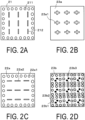
- FIG. 2A is a top view illustrating an embodiment of the insulating substrate 21 included in the antenna substrate 2.
- the insulating substrate 21 is not particularly limited as long as it is formed of a material having an insulating property.
- a material having an insulating property include resins such as an epoxy resin, a bismaleimide-triazine resin, a polyimide resin, and a polyphenylene ether resin. Two or more of these resins may be mixed and used.
- the insulating substrate 21 may contain a reinforcing material.
- the reinforcing material include insulation fabric materials such as glass fiber, glass non-woven fabric, aramid non-woven fabric, aramid fiber, and polyester fiber. Two or more types of reinforcing materials may be used in combination.
- an inorganic insulating filler made of silica, barium sulfate, talc, clay, glass, calcium carbonate, titanium oxide, or the like may be dispersed in the insulating substrate 21.
- the second antenna conductors 212 are located and pads 211 are located in a peripheral edge portion of the insulating substrate 21 so as to surround the second antenna conductors 212.
- the second antenna conductor 212 and the pad 211 are not limited as long as they are formed of a material having electrical conductivity. Examples of a material having electrical conductivity include metals such as copper.
- the second antenna conductor 212 and the pad 211 are formed of a metal foil such as a copper foil or metal plating such as copper plating.
- the second antenna conductor 212 has, for example, a vertically straight line shape and is provided so as to receive and transmit electromagnetic waves.
- the insulating layer 22b is located so as to cover the upper surface of the insulating substrate 21, the second antenna conductors 212, and the pads 211. Similarly to the insulating substrate 21, the insulating layer 22b is formed of a material having an insulating property as described above and may contain a reinforcing material and an inorganic insulating filler as described above.
- the first grounding conductor layer 23a is located on an upper surface of the insulating layer 22b.
- FIG. 2B is a top view illustrating an embodiment of the first grounding conductor layer 23a included in the antenna substrate 2.
- the first grounding conductor layer 23a is not limited as long as it is formed of a conductor, and is formed of, for example, a metal foil such as a copper foil or metal plating such as copper plating.
- the first grounding conductor layer 23a is provided with slots 23a1 each substantially facing a place where the corresponding second antenna conductor 212 and the corresponding first antenna conductor 22a2 to be described later are located.
- the slot 23a1 has a cross shape, in conformity to shapes of the second antenna conductor 212 having a vertically straight line shape and the first antenna conductor 22a2 having a horizontally straight line shape.
- the slot 23a1 is formed by, for example, etching a solid conductor that is a precursor of the first grounding conductor layer 23a.
- the insulating layer 22a is located on an upper surface of the first grounding conductor layer 23a.
- FIG. 2C is a top view illustrating an embodiment of the insulating layer 22a included in the antenna substrate 2.
- the first antenna conductors 22a2 are located and pads 22a1 are located in a peripheral edge portion of the insulating layer 22a so as to surround the first antenna conductors 22a2.
- the first antenna conductor 22a2 and the pad 22a1 are formed of a metal such as copper, specifically, a metal foil such as a copper foil or metal plating such as copper plating.
- the first antenna conductor 22a2 has a horizontally straight line shape and is located at a position facing the second antenna conductor 212 so as to intersect the second antenna conductor 212. That is, the first antenna conductor 22a2 and the second antenna conductor 212 form a cross shape in a plane perspective.
- the antenna substrate 2 may have a configuration that allows transmission and reception of only radio waves in one frequency band when radio waves having different frequencies are mixed. That is, it is preferable that the antenna substrate has a resonance point limited by adjusting arrangement or the like of the first antenna conductors 22a2, the second antenna conductors 212, and the slots 23a1.
- the structure of the antenna structure 1 can be further simplified, which can contribute to, for example, miniaturization.
- FIG. 2D is a top view illustrating an embodiment of the second grounding conductor layer 23b included in the antenna substrate 2. Furthermore, on the lower surface of the insulating substrate 21, a first electrode 23b1, a second electrode 23b2, and a power supply conductor 23b3 are located with a clearance from the second grounding conductor layer 23b to ensure insulating properties.
- the first electrode 23b 1 is connected to the first antenna conductor 22a2 via the first through-hole conductor 24b.
- the second electrode 23b2 is connected to the second antenna conductor 212 via the second through-hole conductor 24c.
- one set of the first electrode 23b1 and the second electrode 23b2 is located in a region facing the corresponding set of the first antenna conductor 22a2 and the second antenna conductor 212. Specifically, there are nine sets of the first antenna conductor 22a2 and the second antenna conductor 212, and as illustrated in FIG. 2D , one set of the first electrode 23b1 and the second electrode 23b2 is located in the corresponding region of the nine regions.
- the power supply conductors 23b3 are located in a peripheral edge portion of each region so as to surround one set of the first electrode 23b1 and the second electrode 23b2.
- the transmissive filter 3 As illustrated in FIG. 1 , the transmissive filter 3 is located over a first surface (upper surface) of the antenna substrate 2 with the electromagnetic wave guiding layer 4 described later interposed therebetween. As illustrated in FIG. 1 , the transmissive filter 3 includes an insulating substrate 31, first annular patterns 32a located on a lower surface (a surface on the antenna substrate 2 side) of the insulating substrate 31, and second annular patterns 32b located on an upper surface (a surface on an opposite side to the antenna substrate 2 side) of the insulating substrate 31.
- the transmissive filter 3 will be specifically described with reference to FIG. 3 .
- FIG. 3A is a top view illustrating an embodiment of the transmissive filter 3 included in the antenna structure 1
- FIG. 3B is a bottom view illustrating the embodiment of the transmissive filter 3 included in the antenna structure 1.
- the second annular patterns 32b are located and second grounding pads 34b are located in a peripheral edge portion of the insulating substrate 31 so as to surround the second annular patterns 32b.
- the insulating substrate 31 is not particularly limited as long as it is a material having an insulating property, and may further contain a reinforcing material or an inorganic insulating filler.
- the second annular pattern 32b is located in a region facing the corresponding set of the first antenna conductor 22a2 and the second antenna conductor 212 described above.
- the second annular pattern 32b has a circular ring shape and is formed of a metal such as copper, specifically, a metal foil such as a copper foil or metal plating such as copper plating.
- the shape of the second annular pattern 32b is not limited to a circular ring shape, and is not limited as long as it has an annular shape.
- the second grounding pad 34b is not a pad for electrically connecting members, but is used for simply connecting members.
- the second grounding pad 34b may be formed of a metal such as copper, or may be formed of a resin.
- a solder resist 35 is formed in the peripheral edge portion of the insulating substrate 31.
- the solder resist 35 has an opening through which the second grounding pad 34b is exposed.
- the solder resist 35 is formed of, for example, an acryl-modified epoxy resin.
- first annular patterns 32a are located and first grounding pads 34a are located in the peripheral edge portion of the insulating substrate 31 so as to surround the first annular patterns 32a.
- the first annular pattern 32a is located so as to face the second annular pattern 32b with the insulating substrate 31 interposed therebetween.
- the first annular pattern 32a and the second annular pattern 32b are located so as to entirely overlap each other in a plane perspective.
- the first annular pattern 32a also has a circular ring shape and is formed of a metal such as copper, specifically, a metal foil such as a copper foil or metal plating such as copper plating.
- the shape of the first annular pattern 32a is not limited to a circular ring shape, and is not limited as long as it has an annular shape.
- the first grounding pad 34a located on the lower surface of the insulating substrate 31 is not a pad for electrically connecting members, but is used for simply connecting members. For this reason, the first grounding pad 34a located on the lower surface of the insulating substrate 31 may also be made of a metal such as copper, or a resin.
- the solder resist 35 is also formed in a peripheral edge portion of the lower surface of the insulating substrate 31.
- the solder resist 35 located on the lower surface of the insulating substrate 31 also has an opening through which the first grounding pad 34a is exposed.
- the solder resist 35 is formed of, for example, an acryl-modified epoxy resin.
- the first annular pattern 32a and the second annular pattern 32b included in the transmissive filter 3 When a pattern is formed in an annular shape like the first annular pattern 32a and the second annular pattern 32b included in the transmissive filter 3, it is possible to intensify radio waves and to reduce mixing of radio waves with the adjacent annular pattern. As illustrated in FIGs. 3A and 3B , the first annular pattern 32a and the second annular pattern 32b each have a circular shape, and therefore, the effects are further exhibited.
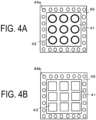
- the electromagnetic wave guiding layer 4 interposed between the antenna substrate 2 and the transmissive filter 3 includes an insulating substrate 41, third annular patterns 42 located on an upper surface (a surface on the transmissive filter 3 side) of the insulating substrate 41, and electromagnetic wave guiding electrodes 43 located on a lower surface (a surface on the antenna substrate 2 side) of the insulating substrate 41.
- the electromagnetic wave guiding layer 4 is used to more efficiently guide radio waves from the antenna substrate 2 to the transmissive filter 3, or to more efficiently guide radio waves transmitting through the transmissive filter 3 from the outside to the antenna substrate 2.
- the electromagnetic wave guiding layer 4 will be specifically described with reference to FIG. 4 .
- FIG. 4A is a top view illustrating an embodiment of the electromagnetic wave guiding layer 4 included in the antenna structure 1
- FIG. 4B is a bottom view illustrating the embodiment of the electromagnetic wave guiding layer 4 included in the antenna structure 1.
- the third annular patterns 42 are formed and third grounding pads 44a are formed in a peripheral edge portion of the insulating substrate 41 so as to surround the third annular patterns 42.
- the insulating substrate 41 is not particularly limited as long as it is a material having an insulating property, and may further contain a reinforcing material or an inorganic insulating filler.
- the third annular patterns 42 are identical in number to the first annular patterns 32a, and are each located so as to face the corresponding first annular pattern 32a. Similarly to the first annular pattern 32a, the third annular pattern 42 also has a circular shape and is formed of a metal such as copper, specifically, a metal foil such as a copper foil or metal plating such as copper plating.
- the shape of the third annular pattern 42 is not limited to a circular ring shape and is not limited as long as it has an annular shape.
- the third grounding pad 44a is not a pad for electrically connecting members, but is used for simply connecting members.
- the third grounding pad 44a may be made of a metal such as copper, or a resin.
- a solder resist 45 is formed in the peripheral edge portion of the insulating substrate 41.
- the solder resist 45 has an opening through which the third grounding pad 44a is exposed.
- the solder resist 45 is formed of, for example, an acryl-modified epoxy resin.
- the electromagnetic wave guiding electrodes 43 are located and fourth grounding pads 44b are located in the peripheral edge portion of the insulating substrate 41 so as to surround the electromagnetic wave guiding electrodes 43.
- the electromagnetic wave guiding electrodes 43 are identical in number to the third annular patterns 42, and are each located so as to face the corresponding third annular pattern 42 with the insulating substrate 41 interposed therebetween.
- a shape of the electromagnetic wave guiding electrode 43 is not an annular shape but a planar quadrangular shape.
- the shape of the electromagnetic wave guiding electrode 43 may also be a polygon other than a quadrangle, or a circle.
- the electromagnetic wave guiding electrode 43 is formed of a metal such as copper, specifically, a metal foil such as a copper foil or metal plating such as copper plating.
- the fourth grounding pad 44b located on the lower surface of the insulating substrate 41 is not a pad for electrically connecting members, but is used for simply connecting members.
- the fourth grounding pad 44b may also be made of a metal such as copper, or a resin.
- the solder resist 45 is also formed in a peripheral edge portion of the lower surface of the insulating substrate 41.
- the solder resist 45 located on the lower surface of the insulating substrate 41 also has an opening through which the fourth grounding pad 44b is exposed.
- the solder resist 45 is formed of, for example, an acryl-modified epoxy resin.
- FIG. 5 is a perspective view illustrating an embodiment of the control substrates 5 included in the antenna structure 1.
- the control substrates 5 are identical in number to the first annular patterns 32a, and are each located so as to face the corresponding first annular pattern 32a. In the present embodiment, nine individual control substrates 5 are arranged in three rows and three columns.
- the control substrate 5 includes an insulating substrate 51, and grounding/power supply electrodes 52, a third electrode 521, and a fourth electrode 522 located on an upper surface of the insulating substrate 51, and is further provided with a control circuit (not illustrated).
- the control substrate 5 functions to control an intensity of electromagnetic waves or timings of transmission and reception of the electromagnetic waves.
- the insulating substrate 51 is not particularly limited as long as it is a material having an insulating property, and may further contain a reinforcing material or an inorganic insulating filler.
- the grounding/power supply electrodes 52 are located in a peripheral edge portion of the insulating substrate 51 so as to surround the third electrode 521 and the fourth electrode 522.
- the grounding/power supply electrode 52 is formed of a metal such as copper, specifically, a metal foil such as a copper foil or metal plating such as copper plating.
- the third electrode 521 is connected to the first antenna conductor 22a2 via the first electrode 23b1 and the first through-hole conductor 24b.
- the fourth electrode 522 is connected to the second antenna conductor 212 via the second electrode 23b2 and the second through-hole conductor 24c.
- the third electrode 521 and the fourth electrode 522 are formed of a metal such as copper, specifically, a metal foil such as a copper foil or metal plating such as copper plating.
- a solder resist 55 is formed in a peripheral edge portion of an upper surface of the insulating substrate 51.
- the solder resist 55 has an opening through which the grounding/power supply electrode 52 is exposed.
- the solder resist 55 is formed of, for example, an acryl-modified epoxy resin.
- semiconductor elements 6 are mounted on a lower surface of the control substrate 5. A gap between the control substrate 5 and each of the semiconductor elements 6 is filled with a sealing resin 7.
- the transmissive filter 3 may be provided with grounding wiring lines 341 (a first grounding wiring line 341a and a second grounding wiring line 341b) to discharge electromotive current.
- the grounding wiring line 341 is formed of a metal such as copper, specifically, a metal foil such as a copper foil or metal plating such as copper plating.
- the grounding wiring lines 341 are located on both surfaces (upper and lower surfaces) of the insulating substrate 31 included in the transmissive filter 3.
- the second grounding wiring line 341b located on the upper surface of the insulating substrate 31 is located so as to connect the second annular pattern 32b and the second grounding pad 34b.
- the grounding pad 34 to which the second grounding wiring line 341b is connected is preferably formed of a metal such as copper.
- the first grounding wiring line 341a located on the lower surface of the insulating substrate 31 is formed so as to connect the first annular pattern 32a and the first grounding pad 34a.
- the first grounding pad 34a to which the first grounding wiring line 341a is connected is preferably made of a metal such as copper.
- the first grounding pad 34a and the second grounding pad 34b are electrically connected via, for example, a via hole conductor located in the insulating substrate 31.
- the antenna structure 1 according to the embodiment described above has a structure in which one transmissive filter 3 is layered.
- the antenna structure of the present disclosure may have a structure in which two or more transmissive filters are layered.
- the solder resists are formed on the upper and lower surfaces of the transmissive filter 3, the upper and lower surfaces of the electromagnetic wave guiding layer 4, and the upper surface of the control substrate 5.
- the solder resists are not essential members and may be used as necessary.
- the electromagnetic wave guiding layer 4 is used in the antenna structure 1 according to the embodiment described above.
- the electromagnetic wave guiding layer is not an essential member and may be used as necessary.
Landscapes
- Engineering & Computer Science (AREA)
- Microelectronics & Electronic Packaging (AREA)
- Physics & Mathematics (AREA)
- Electromagnetism (AREA)
- Details Of Aerials (AREA)
- Aerials With Secondary Devices (AREA)
- Variable-Direction Aerials And Aerial Arrays (AREA)
- Waveguide Aerials (AREA)
Abstract
Description
- The present invention relates to an antenna structure.
- Conventionally, a communication device that uses a wireless network includes an antenna structure as described in
Patent Document 1, for example, for transmission and reception of electrical signals. Such an antenna structure has, for example, a structure in which an electric filter substrate is layered on an upper surface of a control substrate (RF control substrate) and an antenna substrate is layered on an upper surface of the electric filter substrate. - In the antenna structure described in
Patent Document 1, the antenna substrate and the control substrate are connected via the electric filter substrate. This results in longer wiring lines and a higher transmission loss. In addition, since such an antenna structure has a layered structure, when connection failure or the like occurs, each of the antenna substrate, the electric filter substrate, and the control substrate cannot be reused. As a result, the yield is lowered. In order to avoid such defects, a relatively expensive low-dielectric material or low-loss material is employed, which leads to an increase in cost. - In the antenna structure described in
Patent Document 1, the antenna substrate, the electric filter substrate, and the control substrate have substantially the same size in a plan view. Since such an antenna structure has the layered structure, each member cannot be applied with an arbitrary size according to an arrangement location. As a result, it is difficult to miniaturize the antenna structure. - Patent Document 1:
JP 6-152101 A - An antenna structure according to the present disclosure includes an antenna substrate including a first surface and a second surface located on an opposite side to the first surface, a transmissive filter located over the first surface, and a control substrate located on the second surface. The transmissive filter includes a first annular pattern located on a surface facing the first surface, and a second annular pattern located on a surface on an opposite side to the surface facing the first surface. The first annular pattern and the second annular pattern are located overlapping each other in a plane perspective. The control substrate is identical in number to the first annular pattern, and is located overlapping the first annular pattern in a plane perspective.
-
-
FIG. 1 is an explanatory view illustrating an antenna structure according to an embodiment of the present disclosure. -
FIGs. 2A to 2D are explanatory views for explaining an antenna substrate included in the antenna structure illustrated inFIG. 1 , in whichFIG. 2A is a top view illustrating an embodiment of an insulating substrate,FIG. 2B is a top view illustrating an embodiment of a first grounding conductor layer,FIG. 2C is a top view illustrating an embodiment of an insulating layer located on an uppermost surface, andFIG. 2D is a top view illustrating an embodiment of a second grounding conductor layer. -
FIG. 3A is a top view illustrating an embodiment of a transmissive filter included in the antenna structure illustrated inFIG. 1 , andFIG. 3B is a bottom view illustrating the embodiment of the transmissive filter included in the antenna structure illustrated inFIG. 1 . -
FIG. 4A is a top view illustrating an embodiment of an electromagnetic wave guiding layer included in the antenna structure illustrated inFIG. 1 , andFIG. 4B is a bottom view illustrating the embodiment of the electromagnetic wave guiding layer included in the antenna structure illustrated inFIG. 1 . -
FIG. 5 is a perspective view illustrating an embodiment of a control substrate included in the antenna structure illustrated inFIG. 1 . -
FIG. 6A is a top view illustrating another embodiment of the transmissive filter included in the antenna structure illustrated inFIG. 1 , andFIG. 6B is a bottom view illustrating the another embodiment of the transmissive filter included in the antenna structure illustrated inFIG. 1 . - As described above, the conventional antenna structure has a structure in which an electric filter substrate is layered on an upper surface of a control substrate (RF control substrate) and an antenna substrate is layered on an upper surface of the electric filter substrate. For this reason, as described above, the yield may decrease, the cost may increase, or each member cannot be applied in an arbitrary size according to an arrangement location. Therefore, there is a need for an antenna structure that has a low transmission loss, a high yield, and a low cost and in which each member can be applied with an arbitrary size according to an arrangement location.
- An antenna structure according to the present disclosure includes a transmissive filter located over a first surface of an antenna substrate, and at least one control substrate located on a second surface of the antenna substrate. In addition, the antenna structure according to the present disclosure is not an integrated laminate of the antenna substrate, the control substrate, and the transmissive filter, but has a structure in which individual members are bonded. Therefore, according to the present disclosure, it is possible to provide an antenna structure that has a low transmission loss, a high yield, and a low cost and in which each member can be applied with an arbitrary size according to an arrangement location.
- An antenna structure according to an embodiment of the present disclosure will be described below with reference to
FIGs. 1 to 5 . As illustrated inFIG. 1 , anantenna structure 1 according to an embodiment includes anantenna substrate 2, atransmissive filter 3, an electromagneticwave guiding layer 4, and acontrol substrate 5. - The
antenna substrate 2 has a structure in whichsecond antenna conductors 212, an insulating layer (second insulating layer) 22b, a firstgrounding conductor layer 23a, an insulating layer (first insulating layer) 22a, and first antenna conductors 22a2 are layered in this order on an upper surface of aninsulating substrate 21 and a secondgrounding conductor layer 23b is layered on a lower surface of theinsulating substrate 21. Furthermore, theantenna substrate 2 includes grounding/power supply through-hole conductors 24a penetrating through upper and lower surfaces of theantenna substrate 2, first through-hole conductors 24b each electrically connecting the corresponding first antenna conductor 22a2 and thecorresponding control substrate 5, and second through-hole conductors 24c each electrically connecting the correspondingsecond antenna conductor 212 and thecorresponding control substrate 5. The grounding/power supply through-hole conductor 24a, the first through-hole conductor 24b, and the second through-hole conductor 24c are formed of a metal such as copper. - The
antenna substrate 2 will be specifically described with reference toFIGs. 2A to 2D. FIG. 2A is a top view illustrating an embodiment of theinsulating substrate 21 included in theantenna substrate 2. Theinsulating substrate 21 is not particularly limited as long as it is formed of a material having an insulating property. Examples of a material having an insulating property include resins such as an epoxy resin, a bismaleimide-triazine resin, a polyimide resin, and a polyphenylene ether resin. Two or more of these resins may be mixed and used. - The
insulating substrate 21 may contain a reinforcing material. Examples of the reinforcing material include insulation fabric materials such as glass fiber, glass non-woven fabric, aramid non-woven fabric, aramid fiber, and polyester fiber. Two or more types of reinforcing materials may be used in combination. In addition, an inorganic insulating filler made of silica, barium sulfate, talc, clay, glass, calcium carbonate, titanium oxide, or the like may be dispersed in theinsulating substrate 21. - On the upper surface of the
insulating substrate 21, thesecond antenna conductors 212 are located andpads 211 are located in a peripheral edge portion of theinsulating substrate 21 so as to surround thesecond antenna conductors 212. Thesecond antenna conductor 212 and thepad 211 are not limited as long as they are formed of a material having electrical conductivity. Examples of a material having electrical conductivity include metals such as copper. Specifically, thesecond antenna conductor 212 and thepad 211 are formed of a metal foil such as a copper foil or metal plating such as copper plating. - The
second antenna conductor 212 has, for example, a vertically straight line shape and is provided so as to receive and transmit electromagnetic waves. - The insulating
layer 22b is located so as to cover the upper surface of the insulatingsubstrate 21, thesecond antenna conductors 212, and thepads 211. Similarly to the insulatingsubstrate 21, the insulatinglayer 22b is formed of a material having an insulating property as described above and may contain a reinforcing material and an inorganic insulating filler as described above. - The first
grounding conductor layer 23a is located on an upper surface of the insulatinglayer 22b.FIG. 2B is a top view illustrating an embodiment of the firstgrounding conductor layer 23a included in theantenna substrate 2. The firstgrounding conductor layer 23a is not limited as long as it is formed of a conductor, and is formed of, for example, a metal foil such as a copper foil or metal plating such as copper plating. - The first
grounding conductor layer 23a is provided with slots 23a1 each substantially facing a place where the correspondingsecond antenna conductor 212 and the corresponding first antenna conductor 22a2 to be described later are located. The slot 23a1 has a cross shape, in conformity to shapes of thesecond antenna conductor 212 having a vertically straight line shape and the first antenna conductor 22a2 having a horizontally straight line shape. The slot 23a1 is formed by, for example, etching a solid conductor that is a precursor of the firstgrounding conductor layer 23a. - The insulating
layer 22a is located on an upper surface of the firstgrounding conductor layer 23a.FIG. 2C is a top view illustrating an embodiment of the insulatinglayer 22a included in theantenna substrate 2. On an upper surface of the insulatinglayer 22a, the first antenna conductors 22a2 are located and pads 22a1 are located in a peripheral edge portion of the insulatinglayer 22a so as to surround the first antenna conductors 22a2. Similarly to thesecond antenna conductor 212 and thepad 211, the first antenna conductor 22a2 and the pad 22a1 are formed of a metal such as copper, specifically, a metal foil such as a copper foil or metal plating such as copper plating. - The first antenna conductor 22a2 has a horizontally straight line shape and is located at a position facing the
second antenna conductor 212 so as to intersect thesecond antenna conductor 212. That is, the first antenna conductor 22a2 and thesecond antenna conductor 212 form a cross shape in a plane perspective. - The
antenna substrate 2 may have a configuration that allows transmission and reception of only radio waves in one frequency band when radio waves having different frequencies are mixed. That is, it is preferable that the antenna substrate has a resonance point limited by adjusting arrangement or the like of the first antenna conductors 22a2, thesecond antenna conductors 212, and the slots 23a1. When theantenna substrate 2 has a configuration that allows transmission and reception of only radio waves in one frequency band, the structure of theantenna structure 1 can be further simplified, which can contribute to, for example, miniaturization. - On the other hand, the second
grounding conductor layer 23b is located on the lower surface of the insulatingsubstrate 21.FIG. 2D is a top view illustrating an embodiment of the secondgrounding conductor layer 23b included in theantenna substrate 2. Furthermore, on the lower surface of the insulatingsubstrate 21, a first electrode 23b1, a second electrode 23b2, and a power supply conductor 23b3 are located with a clearance from the secondgrounding conductor layer 23b to ensure insulating properties. Thefirst electrode 23bhole conductor 24b. The second electrode 23b2 is connected to thesecond antenna conductor 212 via the second through-hole conductor 24c. - In the
antenna substrate 2, one set of the first electrode 23b1 and the second electrode 23b2 is located in a region facing the corresponding set of the first antenna conductor 22a2 and thesecond antenna conductor 212. Specifically, there are nine sets of the first antenna conductor 22a2 and thesecond antenna conductor 212, and as illustrated inFIG. 2D , one set of the first electrode 23b1 and the second electrode 23b2 is located in the corresponding region of the nine regions. The power supply conductors 23b3 are located in a peripheral edge portion of each region so as to surround one set of the first electrode 23b1 and the second electrode 23b2. - Next, the
transmissive filter 3 will be described. As illustrated inFIG. 1 , thetransmissive filter 3 is located over a first surface (upper surface) of theantenna substrate 2 with the electromagneticwave guiding layer 4 described later interposed therebetween. As illustrated inFIG. 1 , thetransmissive filter 3 includes an insulatingsubstrate 31, firstannular patterns 32a located on a lower surface (a surface on theantenna substrate 2 side) of the insulatingsubstrate 31, and secondannular patterns 32b located on an upper surface (a surface on an opposite side to theantenna substrate 2 side) of the insulatingsubstrate 31. Thetransmissive filter 3 will be specifically described with reference toFIG. 3 . -
FIG. 3A is a top view illustrating an embodiment of thetransmissive filter 3 included in theantenna structure 1, andFIG. 3B is a bottom view illustrating the embodiment of thetransmissive filter 3 included in theantenna structure 1. As illustrated inFIG. 3A , on the upper surface of the insulatingsubstrate 31, the secondannular patterns 32b are located andsecond grounding pads 34b are located in a peripheral edge portion of the insulatingsubstrate 31 so as to surround the secondannular patterns 32b. - Similarly to the insulating
substrate 21 described above, the insulatingsubstrate 31 is not particularly limited as long as it is a material having an insulating property, and may further contain a reinforcing material or an inorganic insulating filler. - The second
annular pattern 32b is located in a region facing the corresponding set of the first antenna conductor 22a2 and thesecond antenna conductor 212 described above. The secondannular pattern 32b has a circular ring shape and is formed of a metal such as copper, specifically, a metal foil such as a copper foil or metal plating such as copper plating. The shape of the secondannular pattern 32b is not limited to a circular ring shape, and is not limited as long as it has an annular shape. - In the present embodiment, the
second grounding pad 34b is not a pad for electrically connecting members, but is used for simply connecting members. For this reason, thesecond grounding pad 34b may be formed of a metal such as copper, or may be formed of a resin. - A solder resist 35 is formed in the peripheral edge portion of the insulating
substrate 31. The solder resist 35 has an opening through which thesecond grounding pad 34b is exposed. The solder resist 35 is formed of, for example, an acryl-modified epoxy resin. - On the other hand, as illustrated in
FIG. 3B , on the lower surface of the insulatingsubstrate 31, the firstannular patterns 32a are located andfirst grounding pads 34a are located in the peripheral edge portion of the insulatingsubstrate 31 so as to surround the firstannular patterns 32a. - The first
annular pattern 32a is located so as to face the secondannular pattern 32b with the insulatingsubstrate 31 interposed therebetween. In other words, the firstannular pattern 32a and the secondannular pattern 32b are located so as to entirely overlap each other in a plane perspective. Similarly to the secondannular pattern 32b, the firstannular pattern 32a also has a circular ring shape and is formed of a metal such as copper, specifically, a metal foil such as a copper foil or metal plating such as copper plating. The shape of the firstannular pattern 32a is not limited to a circular ring shape, and is not limited as long as it has an annular shape. - In the present embodiment, the
first grounding pad 34a located on the lower surface of the insulatingsubstrate 31 is not a pad for electrically connecting members, but is used for simply connecting members. For this reason, thefirst grounding pad 34a located on the lower surface of the insulatingsubstrate 31 may also be made of a metal such as copper, or a resin. - Similarly to the peripheral edge portion of the upper surface of the insulating
substrate 31, the solder resist 35 is also formed in a peripheral edge portion of the lower surface of the insulatingsubstrate 31. The solder resist 35 located on the lower surface of the insulatingsubstrate 31 also has an opening through which thefirst grounding pad 34a is exposed. As described above, the solder resist 35 is formed of, for example, an acryl-modified epoxy resin. - When a pattern is formed in an annular shape like the first
annular pattern 32a and the secondannular pattern 32b included in thetransmissive filter 3, it is possible to intensify radio waves and to reduce mixing of radio waves with the adjacent annular pattern. As illustrated inFIGs. 3A and 3B , the firstannular pattern 32a and the secondannular pattern 32b each have a circular shape, and therefore, the effects are further exhibited. - As illustrated in
FIG. 1 , the electromagneticwave guiding layer 4 interposed between theantenna substrate 2 and thetransmissive filter 3 includes an insulatingsubstrate 41, thirdannular patterns 42 located on an upper surface (a surface on thetransmissive filter 3 side) of the insulatingsubstrate 41, and electromagneticwave guiding electrodes 43 located on a lower surface (a surface on theantenna substrate 2 side) of the insulatingsubstrate 41. The electromagneticwave guiding layer 4 is used to more efficiently guide radio waves from theantenna substrate 2 to thetransmissive filter 3, or to more efficiently guide radio waves transmitting through thetransmissive filter 3 from the outside to theantenna substrate 2. The electromagneticwave guiding layer 4 will be specifically described with reference toFIG. 4 . -
FIG. 4A is a top view illustrating an embodiment of the electromagneticwave guiding layer 4 included in theantenna structure 1, andFIG. 4B is a bottom view illustrating the embodiment of the electromagneticwave guiding layer 4 included in theantenna structure 1. As illustrated inFIG. 4A , on the upper surface of the insulatingsubstrate 41, the thirdannular patterns 42 are formed andthird grounding pads 44a are formed in a peripheral edge portion of the insulatingsubstrate 41 so as to surround the thirdannular patterns 42. - Similarly to the insulating
substrate 21 described above, the insulatingsubstrate 41 is not particularly limited as long as it is a material having an insulating property, and may further contain a reinforcing material or an inorganic insulating filler. - The third
annular patterns 42 are identical in number to the firstannular patterns 32a, and are each located so as to face the corresponding firstannular pattern 32a. Similarly to the firstannular pattern 32a, the thirdannular pattern 42 also has a circular shape and is formed of a metal such as copper, specifically, a metal foil such as a copper foil or metal plating such as copper plating. The shape of the thirdannular pattern 42 is not limited to a circular ring shape and is not limited as long as it has an annular shape. - In the present embodiment, the
third grounding pad 44a is not a pad for electrically connecting members, but is used for simply connecting members. For this reason, thethird grounding pad 44a may be made of a metal such as copper, or a resin. - A solder resist 45 is formed in the peripheral edge portion of the insulating
substrate 41. The solder resist 45 has an opening through which thethird grounding pad 44a is exposed. As described above, the solder resist 45 is formed of, for example, an acryl-modified epoxy resin. - On the other hand, as illustrated in
FIG. 4B , on the lower surface of the insulatingsubstrate 41, the electromagneticwave guiding electrodes 43 are located andfourth grounding pads 44b are located in the peripheral edge portion of the insulatingsubstrate 41 so as to surround the electromagneticwave guiding electrodes 43. - The electromagnetic
wave guiding electrodes 43 are identical in number to the thirdannular patterns 42, and are each located so as to face the corresponding thirdannular pattern 42 with the insulatingsubstrate 41 interposed therebetween. A shape of the electromagneticwave guiding electrode 43 is not an annular shape but a planar quadrangular shape. The shape of the electromagneticwave guiding electrode 43 may also be a polygon other than a quadrangle, or a circle. The electromagneticwave guiding electrode 43 is formed of a metal such as copper, specifically, a metal foil such as a copper foil or metal plating such as copper plating. - In the present embodiment, the
fourth grounding pad 44b located on the lower surface of the insulatingsubstrate 41 is not a pad for electrically connecting members, but is used for simply connecting members. For this reason, thefourth grounding pad 44b may also be made of a metal such as copper, or a resin. - As in the peripheral edge portion of the upper surface of the insulating
substrate 41, the solder resist 45 is also formed in a peripheral edge portion of the lower surface of the insulatingsubstrate 41. The solder resist 45 located on the lower surface of the insulatingsubstrate 41 also has an opening through which thefourth grounding pad 44b is exposed. As described above, the solder resist 45 is formed of, for example, an acryl-modified epoxy resin. - Next, the
control substrates 5 located on a second surface (lower surface) of theantenna substrate 2 will be specifically described with reference toFIG. 5. FIG. 5 is a perspective view illustrating an embodiment of thecontrol substrates 5 included in theantenna structure 1. Thecontrol substrates 5 are identical in number to the firstannular patterns 32a, and are each located so as to face the corresponding firstannular pattern 32a. In the present embodiment, nineindividual control substrates 5 are arranged in three rows and three columns. As illustrated inFIG. 5 , thecontrol substrate 5 includes an insulatingsubstrate 51, and grounding/power supply electrodes 52, athird electrode 521, and afourth electrode 522 located on an upper surface of the insulatingsubstrate 51, and is further provided with a control circuit (not illustrated). Thecontrol substrate 5 functions to control an intensity of electromagnetic waves or timings of transmission and reception of the electromagnetic waves. - Similarly to the insulating
substrate 21 described above, the insulatingsubstrate 51 is not particularly limited as long as it is a material having an insulating property, and may further contain a reinforcing material or an inorganic insulating filler. - The grounding/
power supply electrodes 52 are located in a peripheral edge portion of the insulatingsubstrate 51 so as to surround thethird electrode 521 and thefourth electrode 522. The grounding/power supply electrode 52 is formed of a metal such as copper, specifically, a metal foil such as a copper foil or metal plating such as copper plating. - The
third electrode 521 is connected to the first antenna conductor 22a2 via the first electrode 23b1 and the first through-hole conductor 24b. Thefourth electrode 522 is connected to thesecond antenna conductor 212 via the second electrode 23b2 and the second through-hole conductor 24c. Thethird electrode 521 and thefourth electrode 522 are formed of a metal such as copper, specifically, a metal foil such as a copper foil or metal plating such as copper plating. - A solder resist 55 is formed in a peripheral edge portion of an upper surface of the insulating
substrate 51. The solder resist 55 has an opening through which the grounding/power supply electrode 52 is exposed. As described above, the solder resist 55 is formed of, for example, an acryl-modified epoxy resin. - As illustrated in
FIG. 1 ,semiconductor elements 6 are mounted on a lower surface of thecontrol substrate 5. A gap between thecontrol substrate 5 and each of thesemiconductor elements 6 is filled with a sealingresin 7. - The present disclosure is not limited to the
antenna structure 1 according to the embodiment described above, and various modifications can be made without departing from the scope of the present disclosure. For example, thetransmissive filter 3 may be provided with grounding wiring lines 341 (a firstgrounding wiring line 341a and a secondgrounding wiring line 341b) to discharge electromotive current. Thegrounding wiring line 341 is formed of a metal such as copper, specifically, a metal foil such as a copper foil or metal plating such as copper plating. - As illustrated in
FIGs. 6A and 6B , thegrounding wiring lines 341 are located on both surfaces (upper and lower surfaces) of the insulatingsubstrate 31 included in thetransmissive filter 3. The secondgrounding wiring line 341b located on the upper surface of the insulatingsubstrate 31 is located so as to connect the secondannular pattern 32b and thesecond grounding pad 34b. Thegrounding pad 34 to which the secondgrounding wiring line 341b is connected is preferably formed of a metal such as copper. - The first
grounding wiring line 341a located on the lower surface of the insulatingsubstrate 31 is formed so as to connect the firstannular pattern 32a and thefirst grounding pad 34a. Thefirst grounding pad 34a to which the firstgrounding wiring line 341a is connected is preferably made of a metal such as copper. Thefirst grounding pad 34a and thesecond grounding pad 34b are electrically connected via, for example, a via hole conductor located in the insulatingsubstrate 31. - The
antenna structure 1 according to the embodiment described above has a structure in which onetransmissive filter 3 is layered. However, the antenna structure of the present disclosure may have a structure in which two or more transmissive filters are layered. - In the
antenna structure 1 according to the embodiment described above, the solder resists are formed on the upper and lower surfaces of thetransmissive filter 3, the upper and lower surfaces of the electromagneticwave guiding layer 4, and the upper surface of thecontrol substrate 5. However, in the antenna structure of the present disclosure, the solder resists are not essential members and may be used as necessary. - The electromagnetic
wave guiding layer 4 is used in theantenna structure 1 according to the embodiment described above. However, in the antenna structure of the present disclosure, the electromagnetic wave guiding layer is not an essential member and may be used as necessary. -
- 1 Antenna structure
- 2 Antenna substrate
- 21 Insulating substrate
- 211 Pad
- 212 Second antenna conductor
- 22a First insulating layer
- 22a1 Pad
- 22a2 First antenna conductor
- 22b Second insulating layer
- 23a First grounding conductor layer
- 23a1 Slot
- 23b Second grounding conductor layer
- 23b1 First electrode
- 23b2 Second electrode
- 23b3 Power supply conductor
- 24a Grounding/power supply through-hole conductor
- 24b First through-hole conductor
- 24c Second through-hole conductor
- 3 Transmissive filter
- 31 Insulating substrate
- 32a First annular pattern
- 32b Second annular pattern
- 34 Grounding pad
- 34a First grounding pad
- 34b Second grounding pad
- 341 Grounding wiring line
- 341a First grounding wiring line
- 341b Second grounding wiring line
- 35 Solder resist
- 4 Electromagnetic wave guiding layer
- 41 Insulating substrate
- 42 Third annular pattern
- 43 Electromagnetic wave guiding electrode
- 44a Third grounding pad
- 44b Fourth grounding pad
- 45 Solder resist
- 5 Control substrate
- 51 Insulating substrate
- 52 Grounding/power supply electrode
- 521 Third electrode
- 522 Fourth electrode
- 55 Solder resist
- 6 Semiconductor element
- 7 Sealing resin
Claims (7)
- An antenna structure comprising:an antenna substrate comprising a first surface and a second surface located on an opposite side to the first surface;a transmissive filter located over the first surface; anda control substrate located on the second surface,wherein the transmissive filter comprises a first annular pattern located on a surface facing the first surface, and a second annular pattern located on a surface on an opposite side to the surface facing the first surface,the first annular pattern and the second annular pattern are located overlapping each other in a plane perspective, andthe control substrate is identical in number to the first annular pattern, and is located overlapping the first annular pattern in a plane perspective.
- The antenna structure according to claim 1, further comprising an electromagnetic wave guiding layer located between the antenna substrate and the transmissive filter.
- The antenna structure according to claim 2, wherein the electromagnetic wave guiding layer comprises a third annular pattern on a surface on a side of the transmissive filter, the third annular pattern being identical in number to the first annular pattern and being located facing the first annular pattern, and comprises an electromagnetic wave guiding electrode on a surface on an opposite side, the electromagnetic wave guiding electrode being identical in number to the third annular pattern and being located overlapping the third annular pattern in a plane perspective.
- The antenna structure according to any one of claims 1 to 3, wherein, in the transmissive filter, a first grounding pad is further located in a peripheral edge portion of a surface on the antenna substrate side, and a second grounding pad is further located in a peripheral edge portion of a surface on an opposite side, the first annular pattern and the first grounding pad are connected via a first grounding wiring line, and the second annular pattern and the second grounding pad are connected via a second grounding wiring line.
- The antenna structure according to any one of claims 1 to 4, wherein the first annular pattern, the second annular pattern, and the third annular pattern each have a circular ring shape.
- The antenna structure according to any one of claims 1 to 5, wherein two or more layers of the transmissive filter are layered.
- The antenna structure according to any one of claims 1 to 6, wherein at least one selected from the group consisting of the first annular pattern, the second annular pattern, the third annular pattern, the first grounding pad, the second grounding pad, the first grounding wiring line, and the second grounding wiring line is made of copper.
Applications Claiming Priority (2)
| Application Number | Priority Date | Filing Date | Title |
|---|---|---|---|
| JP2020197305 | 2020-11-27 | ||
| PCT/JP2021/042474 WO2022113884A1 (en) | 2020-11-27 | 2021-11-18 | Antenna structure |
Publications (2)
| Publication Number | Publication Date |
|---|---|
| EP4254666A1 true EP4254666A1 (en) | 2023-10-04 |
| EP4254666A4 EP4254666A4 (en) | 2024-10-30 |
Family
ID=81754571
Family Applications (1)
| Application Number | Title | Priority Date | Filing Date |
|---|---|---|---|
| EP21897858.3A Withdrawn EP4254666A4 (en) | 2020-11-27 | 2021-11-18 | Antenna structure |
Country Status (6)
| Country | Link |
|---|---|
| US (1) | US20240022004A1 (en) |
| EP (1) | EP4254666A4 (en) |
| JP (1) | JP7585346B2 (en) |
| KR (1) | KR102763741B1 (en) |
| CN (1) | CN116615841A (en) |
| WO (1) | WO2022113884A1 (en) |
Families Citing this family (2)
| Publication number | Priority date | Publication date | Assignee | Title |
|---|---|---|---|---|
| KR20230052577A (en) * | 2021-10-13 | 2023-04-20 | 삼성전기주식회사 | Chip patch antenna and chip patch antenna module |
| TW202401898A (en) * | 2022-06-24 | 2024-01-01 | 方略電子股份有限公司 | Antenna device |
Family Cites Families (20)
| Publication number | Priority date | Publication date | Assignee | Title |
|---|---|---|---|---|
| JP2680234B2 (en) | 1992-11-12 | 1997-11-19 | 株式会社日立製作所 | Wiring pattern forming method |
| JPH06177639A (en) * | 1992-12-08 | 1994-06-24 | Nippon Telegr & Teleph Corp <Ntt> | Frequency election plate |
| JP2003060430A (en) | 2001-08-17 | 2003-02-28 | Mitsubishi Heavy Ind Ltd | Antenna for reducing unwanted radiation |
| US6597316B2 (en) * | 2001-09-17 | 2003-07-22 | The Mitre Corporation | Spatial null steering microstrip antenna array |
| US7812767B2 (en) * | 2004-09-07 | 2010-10-12 | Nippon Telegraph And Telephone Corporation | Antenna device, array antenna device using the antenna device, module, module array and package module |
| JP2013201711A (en) * | 2012-03-26 | 2013-10-03 | Kyocer Slc Technologies Corp | Antenna substrate |
| TW201503777A (en) * | 2013-05-30 | 2015-01-16 | 京瓷Slc技術股份有限公司 | Wiring substrate |
| KR102173843B1 (en) * | 2014-06-02 | 2020-11-06 | 삼성전자주식회사 | Lens with spatial mixed-order bandpass filter |
| JP6520568B2 (en) * | 2015-08-25 | 2019-05-29 | 住友電気工業株式会社 | Antenna device |
| JP2018121126A (en) * | 2017-01-23 | 2018-08-02 | 株式会社東芝 | Wireless device |
| KR20190050155A (en) * | 2017-11-02 | 2019-05-10 | 삼성전기주식회사 | Semiconductor package and manufacturing method thereof |
| KR102513750B1 (en) * | 2017-11-28 | 2023-03-24 | 삼성전자 주식회사 | Printed circuit board including electro-conductive pattern and electric device including the printed circuit board |
| US11411316B2 (en) * | 2018-03-30 | 2022-08-09 | Tallysman Wireless Inc. | Anti-jamming and reduced interference global positioning system receiver methods and devices |
| US11011827B2 (en) * | 2018-05-11 | 2021-05-18 | Intel IP Corporation | Antenna boards and communication devices |
| JP6777136B2 (en) * | 2018-11-20 | 2020-10-28 | Tdk株式会社 | Antenna module |
| CN209298341U (en) * | 2019-03-18 | 2019-08-23 | Oppo广东移动通信有限公司 | Antenna units and electronic equipment |
| CN113994542A (en) * | 2019-05-24 | 2022-01-28 | 康普技术有限责任公司 | Wireless communication system having patch antenna array supporting large scanning angle radiation |
| US11411321B2 (en) * | 2019-12-05 | 2022-08-09 | Qualcomm Incorporated | Broadband antenna system |
| KR20210152173A (en) * | 2020-06-08 | 2021-12-15 | 삼성전기주식회사 | Chip antenna and antenna module including chip antenna |
| US12476370B2 (en) * | 2023-07-05 | 2025-11-18 | Rockwell Collins, Inc. | Electronically steered antenna substrate embedded resonator filters |
-
2021
- 2021-11-18 JP JP2022565289A patent/JP7585346B2/en active Active
- 2021-11-18 KR KR1020237017582A patent/KR102763741B1/en active Active
- 2021-11-18 EP EP21897858.3A patent/EP4254666A4/en not_active Withdrawn
- 2021-11-18 CN CN202180079380.0A patent/CN116615841A/en active Pending
- 2021-11-18 WO PCT/JP2021/042474 patent/WO2022113884A1/en not_active Ceased
- 2021-11-18 US US18/038,553 patent/US20240022004A1/en not_active Abandoned
Also Published As
| Publication number | Publication date |
|---|---|
| KR20230093476A (en) | 2023-06-27 |
| KR102763741B1 (en) | 2025-02-07 |
| EP4254666A4 (en) | 2024-10-30 |
| WO2022113884A1 (en) | 2022-06-02 |
| US20240022004A1 (en) | 2024-01-18 |
| JPWO2022113884A1 (en) | 2022-06-02 |
| CN116615841A (en) | 2023-08-18 |
| JP7585346B2 (en) | 2024-11-18 |
Similar Documents
| Publication | Publication Date | Title |
|---|---|---|
| JP6238175B2 (en) | Electromagnetic resonance coupler and high-frequency transmission device | |
| US8354975B2 (en) | Electromagnetic band gap element, and antenna and filter using the same | |
| US20250046989A1 (en) | Antenna module, communication device mounted with the same, and circuit board | |
| JP5730159B2 (en) | Antenna board and antenna module | |
| CN102881680B (en) | Semiconductor device and method of manufacturing same | |
| EP4254666A1 (en) | Antenna structure | |
| US10553954B2 (en) | Wireless device | |
| US20120319908A1 (en) | Electronic apparatus | |
| EP3828924A1 (en) | Vertical interconnection structure of a multi-layer substrate | |
| JP2019212870A (en) | Electronic component module | |
| US20220416412A1 (en) | Antenna module | |
| WO2023223952A1 (en) | High-frequency module | |
| WO2020218289A1 (en) | Module component, antenna module, and communication device | |
| US10965022B2 (en) | High-frequency module and communication device | |
| US20250079284A1 (en) | Semiconductor package and semiconductor electronic device | |
| US11901317B2 (en) | Wireless module | |
| EP4092726A1 (en) | Substrate and antenna module | |
| JP2008263360A (en) | High frequency substrate equipment | |
| JP7555422B2 (en) | Antenna Board | |
| JP7577187B2 (en) | Circularly polarized array antenna and electronic device | |
| US12542357B2 (en) | Antenna, array antenna, semiconductor chip, and wireless apparatus | |
| US20240372259A1 (en) | Antenna device and method for manufacturing antenna device | |
| JP2025086182A (en) | High frequency module and communication device | |
| JP2025111092A (en) | Antenna Module | |
| WO2025009273A1 (en) | Ic-mounted substrate |
Legal Events
| Date | Code | Title | Description |
|---|---|---|---|
| STAA | Information on the status of an ep patent application or granted ep patent |
Free format text: STATUS: THE INTERNATIONAL PUBLICATION HAS BEEN MADE |
|
| PUAI | Public reference made under article 153(3) epc to a published international application that has entered the european phase |
Free format text: ORIGINAL CODE: 0009012 |
|
| STAA | Information on the status of an ep patent application or granted ep patent |
Free format text: STATUS: REQUEST FOR EXAMINATION WAS MADE |
|
| 17P | Request for examination filed |
Effective date: 20230524 |
|
| AK | Designated contracting states |
Kind code of ref document: A1 Designated state(s): AL AT BE BG CH CY CZ DE DK EE ES FI FR GB GR HR HU IE IS IT LI LT LU LV MC MK MT NL NO PL PT RO RS SE SI SK SM TR |
|
| DAV | Request for validation of the european patent (deleted) | ||
| DAX | Request for extension of the european patent (deleted) | ||
| REG | Reference to a national code |
Ref country code: DE Ref legal event code: R079 Free format text: PREVIOUS MAIN CLASS: H01Q0019060000 Ipc: H01Q0001220000 |
|
| A4 | Supplementary search report drawn up and despatched |
Effective date: 20240930 |
|
| RIC1 | Information provided on ipc code assigned before grant |
Ipc: H01Q 15/00 20060101ALI20240924BHEP Ipc: H01Q 21/06 20060101ALI20240924BHEP Ipc: H01Q 21/24 20060101ALI20240924BHEP Ipc: H01Q 9/04 20060101ALI20240924BHEP Ipc: H01Q 1/22 20060101AFI20240924BHEP |
|
| STAA | Information on the status of an ep patent application or granted ep patent |
Free format text: STATUS: THE APPLICATION HAS BEEN WITHDRAWN |
|
| 18W | Application withdrawn |
Effective date: 20250806 |