EP4254653A1 - High-frequency power distributor - Google Patents
High-frequency power distributor Download PDFInfo
- Publication number
- EP4254653A1 EP4254653A1 EP21897877.3A EP21897877A EP4254653A1 EP 4254653 A1 EP4254653 A1 EP 4254653A1 EP 21897877 A EP21897877 A EP 21897877A EP 4254653 A1 EP4254653 A1 EP 4254653A1
- Authority
- EP
- European Patent Office
- Prior art keywords
- microstrip line
- microstrip
- frequency power
- output end
- lines
- Prior art date
- Legal status (The legal status is an assumption and is not a legal conclusion. Google has not performed a legal analysis and makes no representation as to the accuracy of the status listed.)
- Pending
Links
Images


Classifications
-
- H—ELECTRICITY
- H01—ELECTRIC ELEMENTS
- H01P—WAVEGUIDES; RESONATORS, LINES, OR OTHER DEVICES OF THE WAVEGUIDE TYPE
- H01P5/00—Coupling devices of the waveguide type
- H01P5/12—Coupling devices having more than two ports
- H01P5/16—Conjugate devices, i.e. devices having at least one port decoupled from one other port
- H01P5/19—Conjugate devices, i.e. devices having at least one port decoupled from one other port of the junction type
Definitions
- Embodiments relate to a high-frequency power divider.
- Wilkinson power dividers are used for power distribution in high-frequency bands such as microwaves.
- a Wilkinson power divider is multistaged to increase the bandwidth, the power loss is increased, and the circuit scale becomes large.
- Embodiments provide a high-frequency power divider in which a wider bandwidth is possible.
- a high-frequency power divider includes an insulative substrate and a circuit located on the substrate.
- the circuit includes an input end, a first output end, a second output end, multiple first microstrip lines, multiple second microstrip lines, multiple third microstrip lines, and a resistance element.
- One first microstrip line among the multiple first microstrip lines and one second microstrip line among the multiple second microstrip lines are located between the input end and the first output end.
- Another first microstrip line among the multiple first microstrip lines and another second microstrip line among the multiple second microstrip lines are located between the input end and the second output end.
- the input end is connected to a first end of the one first microstrip line and a first end of the other first microstrip line.
- a second end of the one first microstrip line is connected to a first end of the one second microstrip line; and a second end of the one second microstrip line is connected to the first output end.
- a second end of the other first microstrip line is connected to a first end of the other second microstrip line; and a second end of the other second microstrip line is connected to the second output end.
- a first end of one third microstrip line among the multiple third microstrip lines is connected to the second end of the one first microstrip line and the first end of the one second microstrip line.
- a second end of the one third microstrip line is connected to one end of the resistance element.
- a first end of another third microstrip line among the multiple third microstrip lines is connected to the second end of the other first microstrip line and the first end of the other second microstrip line.
- a second end of the other third microstrip line is connected to another end of the resistance element.
- a phase shift of a high-frequency signal between the first end and the second end of each of the multiple first microstrip lines is 90 degrees; and a phase shift of a high-frequency signal between the first end and the second end of each of the multiple second microstrip lines is 90 degrees.
- a phase shift of a high-frequency signal between the first end and the second end of each of the multiple third microstrip lines is 180 degrees.
- the arrangements and configurations of the portions are described using an X-axis, a Y-axis, and a Z-axis shown in the drawings.
- the X-axis, the Y-axis, and the Z-axis are orthogonal to each other and respectively represent an X-direction, a Y-direction, and a Z-direction. Also, there are cases where the Z-direction is described as up, and the opposite direction is described as down.
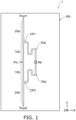
- FIG. 1 is a schematic plan view illustrating a high-frequency power divider 1 according to an embodiment.
- the high-frequency power divider 1 includes, for example, multiple microstrip lines and a resistance element Rb located on a surface of an insulating substrate RS.
- the insulating substrate RS includes, for example, a resin or a ceramic, and includes a not-illustrated metal layer on the back side.
- the multiple microstrip lines include, for example, copper (Cu) or gold (Au).
- the high-frequency power divider 1 includes an input end Pin, a first output end Pout1, a second output end Pout2, multiple first microstrip lines 10a and 10b, multiple second microstrip lines 20a and 20b, multiple third microstrip lines 30a and 30b, and the resistance element Rb.
- the input end Pin, the first output end Pout1, and the second output end Pout2 are arranged along the surface of the insulating substrate RS in a first direction, e.g., the Y-direction.
- the input end Pin is located between the first output end Pout1 and the second output end Pout2.
- the input end Pin and the resistance element Rb are arranged along the surface of the insulating substrate in a second direction, e.g., the X-direction, which crosses the first direction.
- the first microstrip line 10a and the second microstrip line 20a are located between the input end Pin and the first output end Pout1. Also, the first microstrip line 10b and the second microstrip line 20b are located between the input end Pin and the second output end Pout2.
- the first microstrip lines 10a and 10b and the second microstrip lines 20a and 20b each extend in the Y-direction.
- Each of the first microstrip lines 10a and 10b and the second microstrip lines 20a and 20b includes one end (hereinbelow, a first end) and another end (hereinbelow, a second end) without branching.
- the input end Pin is connected to the first end of the first microstrip line 10a and the first end of the first microstrip line 10b.
- the second end of the first microstrip line 10a is connected to the first end of the second microstrip line 20a.
- the second end of the second microstrip line 20a is connected to the first output end Pout1.
- the second end of the first microstrip line 10b is connected to the first end of the second microstrip line 20b.
- the second end of the second microstrip line 20b is connected to the second output end Pout2.
- the third microstrip line 30a is located between the resistance element Rb and a connection point CP1 between the first microstrip line 10a and the second microstrip line 20a.
- a first end of the third microstrip line 30a is connected to the second end of the first microstrip line 10a and the first end of the second microstrip line 20a at the connection point CP1.
- a second end of the third microstrip line 30a is connected to one end of the resistance element Rb.
- the third microstrip line 30b is located between the resistance element Rb and a connection point CP2 between the first microstrip line 10b and the second microstrip line 20b.
- a first end of the third microstrip line 30b is connected to the second end of the first microstrip line 10b and the first end of the second microstrip line 20b at the connection point CP2.
- a second end of the third microstrip line 30b is connected to another end of the resistance element Rb.
- FIG. 2 is a circuit diagram illustrating the high-frequency power divider 1 according to the embodiment. As shown in FIG. 2 , the input end Pin, the first output end Pout1, and the second output end Pout2 are provided so that each has a characteristic impedance Zport of 50 ⁇ .
- the first microstrip lines 10a and 10b are provided so that each has a characteristic impedance Z1 and a phase shift of 90 degrees for the high-frequency signal between the first end and the second end.
- the second microstrip lines 20a and 20b are provided so that each has a characteristic impedance Z2 and a phase shift of 90 degrees for the high-frequency signal between the first end and the second end.
- the third microstrip lines 30a and 30b are provided so that each has a characteristic impedance Z3 and a phase shift of 180 degrees for the high-frequency signal between the first end and the second end.
- FIG. 3 is a graph illustrating a characteristic of the high-frequency power divider 1 according to the embodiment.
- the horizontal axis is the value of the signal frequency normalized by the center frequency.
- the vertical axis is the absolute value of S11 (dB).
- FIG. 3 shows a characteristic SP1 of the high-frequency power divider 1 according to the embodiment and a characteristic SP2 of a high-frequency power divider 2 according to a comparative example (see FIG. 5 ).
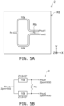
- FIG. 5A is a schematic plan view showing the high-frequency power divider 2; and FIG. 5B is a circuit diagram showing the high-frequency power divider 2.
- the high-frequency power divider 2 is located on a surface of the insulating substrate RS.
- the high-frequency power divider 2 is a Wilkinson power divider.
- the high-frequency power divider 2 includes the input end Pin, the first output end Pout1, the second output end Pout2, the first microstrip line 10a, the first microstrip line 10b, and the resistance element Rb.
- the input end Pin, the first output end Pout1, and the second output end Pout2 are arranged in the X-direction; and the input end Pin and the resistance element Rb also are arranged in the X-direction.
- the first microstrip line 10a is located between the input end Pin and the first output end Pout1.
- the first end of the first microstrip line 10a is connected to the input end Pin; and the second end of the first microstrip line 10a is connected to the one end of the resistance element Rb.
- the first microstrip line 10b is located between the input end Pin and the second output end Pout2.
- the first end of the first microstrip line 10b is connected to the input end Pin; and the second end of the first microstrip line 10b is connected to the other end of the resistance element Rb.
- the first output end Pout1 and the second output end Pout2 are connected respectively to the one end and the other end of the resistance element Rb.
- the input end Pin, the first output end Pout1, and the second output end Pout2 are provided so that each has the characteristic impedance Zport of 50 ⁇ .
- the first microstrip lines 10a and 10b are provided so that each has the characteristic impedance Z1 and a phase shift of 90 degrees for the high-frequency signal between the first end and the second end.
- the characteristic SP2 of the high-frequency power divider 2 has a minimum value at the center frequency.
- the center frequency is, for example, 3 GHz.
- becomes small in the fractional bandwidth range of 0.67 to 1.33 corresponding to the bandwidth of 2 to 4 GHz. For example, looking at the bandwidth where
- the first and second output ends Pout1 and Pout2 of the high-frequency power divider 1 are arranged to be separated from each other in the Y-direction. It is therefore easier to connect to next-stage circuits compared to the high-frequency power divider 2 in which the first output end Pout1 and the second output end Pout2 are located at the two ends of the resistance element Rb.
- FIG. 4 is a circuit diagram illustrating a high-frequency power divider 3 according to a modification of the embodiment.
- the high-frequency power divider 3 has a circuit configuration in which a power divider circuit having the same structure is connected in series to the first output end Pout1 of the power distribution circuit shown in FIG. 2 .
- the high-frequency power divider 3 further includes fourth microstrip lines 40a and 40b, fifth microstrip lines 50a and 50b, sixth microstrip lines 60a and 60b, and a resistance element Rb2.
- the fourth microstrip line 40a and the fifth microstrip line 50a are located between the second microstrip line 20a and the first output end Pout1.
- a first end of the fourth microstrip line 40a is connected to the second end of the second microstrip line 20a; and a second end of the fourth microstrip line 40a is connected to a first end of the fifth microstrip line 50a.
- a second end of the fifth microstrip line 50a is connected to the first output end Pout1.
- the fourth microstrip line 40b and the fifth microstrip line 50b are located between the second microstrip line 20a and the second output end Pout2.
- a first end of the fourth microstrip line 40b is connected to the second end of the second microstrip line 20a; and a second end of the fourth microstrip line 40b is connected to a first end of the fifth microstrip line 50b.
- a second end of the fifth microstrip line 50b is connected to the second output end Pout2.
- the sixth microstrip line 60a is located between the resistance element Rb2 and a connection point CP3 between the fourth microstrip line 40a and the fifth microstrip line 50a.
- a first end of the sixth microstrip line 60a is connected to the second end of the fourth microstrip line 40a and the first end of the fifth microstrip line 50a at the connection point CP3.
- a second end of the third microstrip line 60a is connected to one end of the resistance element Rb2.
- the sixth microstrip line 60b is located between the resistance element Rb2 and a connection point CP4 between the fourth microstrip line 10b and the fifth microstrip line 50b.
- a first end of the sixth microstrip line 60b is connected to the second end of the fourth microstrip line 40b and the first end of the fifth microstrip line 50b at the connection point CP4.
- a second end of the sixth microstrip line 60b is connected to another end of the resistance element Rb2.
- the fourth microstrip lines 40a and 40b are provided so that each has a characteristic impedance Z4 and a phase shift of 90 degrees for the high-frequency signal between the first end and the second end.
- the fifth microstrip lines 50a and 50b are provided so that each has a characteristic impedance Z5 and a phase shift of 90 degrees for the high-frequency signal between the first end and the second end.
- the sixth microstrip lines 60a and 60b are provided so that each has a characteristic impedance Z6 and a phase shift of 180 degrees for the high-frequency signal between the first end and the second end.
- the high-frequency power divider 3 further includes a circuit (not illustrated) similar to FIG. 2 connected to the second microstrip line 20b.
- the high-frequency power divider 3 further includes a third output end Pout3 and a fourth output end Pout4 (not illustrated).
- the embodiments are not limited thereto.
- the number of output ends is 2N.
- a high-frequency power divider that has 2 N output ends can be configured.
Landscapes
- Waveguides (AREA)
- Microwave Amplifiers (AREA)
- Non-Reversible Transmitting Devices (AREA)
Abstract
Description
- Embodiments relate to a high-frequency power divider.
- For example, Wilkinson power dividers are used for power distribution in high-frequency bands such as microwaves. When, however, a Wilkinson power divider is multistaged to increase the bandwidth, the power loss is increased, and the circuit scale becomes large.
- [Patent Literature 1]
JP-A H09-321509 - Embodiments provide a high-frequency power divider in which a wider bandwidth is possible.
- A high-frequency power divider according to an embodiment includes an insulative substrate and a circuit located on the substrate. The circuit includes an input end, a first output end, a second output end, multiple first microstrip lines, multiple second microstrip lines, multiple third microstrip lines, and a resistance element. One first microstrip line among the multiple first microstrip lines and one second microstrip line among the multiple second microstrip lines are located between the input end and the first output end. Another first microstrip line among the multiple first microstrip lines and another second microstrip line among the multiple second microstrip lines are located between the input end and the second output end. The input end is connected to a first end of the one first microstrip line and a first end of the other first microstrip line. A second end of the one first microstrip line is connected to a first end of the one second microstrip line; and a second end of the one second microstrip line is connected to the first output end. A second end of the other first microstrip line is connected to a first end of the other second microstrip line; and a second end of the other second microstrip line is connected to the second output end. A first end of one third microstrip line among the multiple third microstrip lines is connected to the second end of the one first microstrip line and the first end of the one second microstrip line. A second end of the one third microstrip line is connected to one end of the resistance element. A first end of another third microstrip line among the multiple third microstrip lines is connected to the second end of the other first microstrip line and the first end of the other second microstrip line. A second end of the other third microstrip line is connected to another end of the resistance element. A phase shift of a high-frequency signal between the first end and the second end of each of the multiple first microstrip lines is 90 degrees; and a phase shift of a high-frequency signal between the first end and the second end of each of the multiple second microstrip lines is 90 degrees. A phase shift of a high-frequency signal between the first end and the second end of each of the multiple third microstrip lines is 180 degrees.
-
- [
FIG. 1 ]
FIG. 1 is a schematic plan view illustrating a high-frequency power divider according to an embodiment. - [
FIG. 2 ]
FIG. 2 is a circuit diagram illustrating the high-frequency power divider according to the embodiment. - [
FIG. 3 ]
FIG. 3 is a graph illustrating a characteristic of the high-frequency power divider according to the embodiment. - [
FIG. 4 ]
FIG. 4 is a circuit diagram illustrating a high-frequency power divider according to a modification of the embodiment. - [
FIG. 5 ]
FIG. 5 is a circuit diagram and a schematic plan view illustrating a high-frequency power divider according to a comparative example. - Embodiments will now be described with reference to the drawings. The same portions in the drawings are marked with the same numerals; a detailed description is omitted as appropriate; and different portions are described. The drawings are schematic or conceptual; and the relationships between the thickness and width of portions, the proportions of sizes among portions, etc., are not necessarily the same as the actual values. Also, the dimensions and proportions may be illustrated differently among drawings, even when the same portion is illustrated.
- Furthermore, the arrangements and configurations of the portions are described using an X-axis, a Y-axis, and a Z-axis shown in the drawings. The X-axis, the Y-axis, and the Z-axis are orthogonal to each other and respectively represent an X-direction, a Y-direction, and a Z-direction. Also, there are cases where the Z-direction is described as up, and the opposite direction is described as down.
-
FIG. 1 is a schematic plan view illustrating a high-frequency power divider 1 according to an embodiment. The high-frequency power divider 1 includes, for example, multiple microstrip lines and a resistance element Rb located on a surface of an insulating substrate RS. The insulating substrate RS includes, for example, a resin or a ceramic, and includes a not-illustrated metal layer on the back side. The multiple microstrip lines include, for example, copper (Cu) or gold (Au). - As shown in
FIG. 1 , the high-frequency power divider 1 includes an input end Pin, a first output end Pout1, a second output end Pout2, multiplefirst microstrip lines second microstrip lines third microstrip lines 30a and 30b, and the resistance element Rb. - For example, the input end Pin, the first output end Pout1, and the second output end Pout2 are arranged along the surface of the insulating substrate RS in a first direction, e.g., the Y-direction. The input end Pin is located between the first output end Pout1 and the second output end Pout2. Also, for example, the input end Pin and the resistance element Rb are arranged along the surface of the insulating substrate in a second direction, e.g., the X-direction, which crosses the first direction.
- The
first microstrip line 10a and thesecond microstrip line 20a are located between the input end Pin and the first output end Pout1. Also, thefirst microstrip line 10b and thesecond microstrip line 20b are located between the input end Pin and the second output end Pout2. - The
first microstrip lines second microstrip lines first microstrip lines second microstrip lines - The input end Pin is connected to the first end of the
first microstrip line 10a and the first end of thefirst microstrip line 10b. - The second end of the
first microstrip line 10a is connected to the first end of thesecond microstrip line 20a. The second end of thesecond microstrip line 20a is connected to the first output end Pout1. - The second end of the
first microstrip line 10b is connected to the first end of thesecond microstrip line 20b. The second end of thesecond microstrip line 20b is connected to the second output end Pout2. - The
third microstrip line 30a is located between the resistance element Rb and a connection point CP1 between thefirst microstrip line 10a and thesecond microstrip line 20a. A first end of thethird microstrip line 30a is connected to the second end of thefirst microstrip line 10a and the first end of thesecond microstrip line 20a at the connection point CP1. Also, a second end of thethird microstrip line 30a is connected to one end of the resistance element Rb. - The third microstrip line 30b is located between the resistance element Rb and a connection point CP2 between the
first microstrip line 10b and thesecond microstrip line 20b. A first end of the third microstrip line 30b is connected to the second end of thefirst microstrip line 10b and the first end of thesecond microstrip line 20b at the connection point CP2. Also, a second end of the third microstrip line 30b is connected to another end of the resistance element Rb. -
FIG. 2 is a circuit diagram illustrating the high-frequency power divider 1 according to the embodiment. As shown inFIG. 2 , the input end Pin, the first output end Pout1, and the second output end Pout2 are provided so that each has a characteristic impedance Zport of 50 Ω. - The
first microstrip lines - The
second microstrip lines - The
third microstrip lines 30a and 30b are provided so that each has a characteristic impedance Z3 and a phase shift of 180 degrees for the high-frequency signal between the first end and the second end. -
FIG. 3 is a graph illustrating a characteristic of the high-frequency power divider 1 according to the embodiment. The horizontal axis is the value of the signal frequency normalized by the center frequency. The vertical axis is the absolute value of S11 (dB).FIG. 3 shows a characteristic SP1 of the high-frequency power divider 1 according to the embodiment and a characteristic SP2 of a high-frequency power divider 2 according to a comparative example (seeFIG. 5 ). -
FIG. 5A is a schematic plan view showing the high-frequency power divider 2; andFIG. 5B is a circuit diagram showing the high-frequency power divider 2. As shown inFIG. 5A , the high-frequency power divider 2 is located on a surface of the insulating substrate RS. The high-frequency power divider 2 is a Wilkinson power divider. - The high-
frequency power divider 2 includes the input end Pin, the first output end Pout1, the second output end Pout2, thefirst microstrip line 10a, thefirst microstrip line 10b, and the resistance element Rb. For example, the input end Pin, the first output end Pout1, and the second output end Pout2 are arranged in the X-direction; and the input end Pin and the resistance element Rb also are arranged in the X-direction. - The
first microstrip line 10a is located between the input end Pin and the first output end Pout1. The first end of thefirst microstrip line 10a is connected to the input end Pin; and the second end of thefirst microstrip line 10a is connected to the one end of the resistance element Rb. - The
first microstrip line 10b is located between the input end Pin and the second output end Pout2. The first end of thefirst microstrip line 10b is connected to the input end Pin; and the second end of thefirst microstrip line 10b is connected to the other end of the resistance element Rb. - The first output end Pout1 and the second output end Pout2 are connected respectively to the one end and the other end of the resistance element Rb.
- As shown in
FIG. 5B , the input end Pin, the first output end Pout1, and the second output end Pout2 are provided so that each has the characteristic impedance Zport of 50 Ω. Thefirst microstrip lines - As shown in
FIG. 3 , the characteristic SP2 of the high-frequency power divider 2 has a minimum value at the center frequency. The center frequency is, for example, 3 GHz. On the other hand, for example, for the characteristic SP1 of the high-frequency power divider 1, |S11| becomes small in the fractional bandwidth range of 0.67 to 1.33 corresponding to the bandwidth of 2 to 4 GHz. For example, looking at the bandwidth where |S11| is not more than -20 dB, the high-frequency power divider 1 has a wider fractional bandwidth than the high-frequency power divider 2. - Also, as shown in
FIG. 1 , the first and second output ends Pout1 and Pout2 of the high-frequency power divider 1 are arranged to be separated from each other in the Y-direction. It is therefore easier to connect to next-stage circuits compared to the high-frequency power divider 2 in which the first output end Pout1 and the second output end Pout2 are located at the two ends of the resistance element Rb. -
FIG. 4 is a circuit diagram illustrating a high-frequency power divider 3 according to a modification of the embodiment. The high-frequency power divider 3 has a circuit configuration in which a power divider circuit having the same structure is connected in series to the first output end Pout1 of the power distribution circuit shown inFIG. 2 . - As shown in
FIG. 4 , the high-frequency power divider 3 further includesfourth microstrip lines fifth microstrip lines - The
fourth microstrip line 40a and thefifth microstrip line 50a are located between thesecond microstrip line 20a and the first output end Pout1. A first end of thefourth microstrip line 40a is connected to the second end of thesecond microstrip line 20a; and a second end of thefourth microstrip line 40a is connected to a first end of thefifth microstrip line 50a. A second end of thefifth microstrip line 50a is connected to the first output end Pout1. - The
fourth microstrip line 40b and thefifth microstrip line 50b are located between thesecond microstrip line 20a and the second output end Pout2. A first end of thefourth microstrip line 40b is connected to the second end of thesecond microstrip line 20a; and a second end of thefourth microstrip line 40b is connected to a first end of thefifth microstrip line 50b. A second end of thefifth microstrip line 50b is connected to the second output end Pout2. - The sixth microstrip line 60a is located between the resistance element Rb2 and a connection point CP3 between the
fourth microstrip line 40a and thefifth microstrip line 50a. A first end of the sixth microstrip line 60a is connected to the second end of thefourth microstrip line 40a and the first end of thefifth microstrip line 50a at the connection point CP3. Also, a second end of the third microstrip line 60a is connected to one end of the resistance element Rb2. - The sixth microstrip line 60b is located between the resistance element Rb2 and a connection point CP4 between the
fourth microstrip line 10b and thefifth microstrip line 50b. A first end of the sixth microstrip line 60b is connected to the second end of thefourth microstrip line 40b and the first end of thefifth microstrip line 50b at the connection point CP4. Also, a second end of the sixth microstrip line 60b is connected to another end of the resistance element Rb2. - The
fourth microstrip lines - The
fifth microstrip lines - The sixth microstrip lines 60a and 60b are provided so that each has a characteristic impedance Z6 and a phase shift of 180 degrees for the high-frequency signal between the first end and the second end.
- The high-
frequency power divider 3 further includes a circuit (not illustrated) similar toFIG. 2 connected to thesecond microstrip line 20b. The high-frequency power divider 3 further includes a third output end Pout3 and a fourth output end Pout4 (not illustrated). - Although a configuration in which two stages of the circuit shown in
FIG. 2 are connected is shown in the example, the embodiments are not limited thereto. For example, when N stages of the circuit shown inFIG. 2 are included, the number of output ends is 2N. In other words, a high-frequency power divider that has 2N output ends can be configured. - While certain embodiments of the inventions have been described, these embodiments have been presented by way of example only, and are not intended to limit the scope of the inventions. These novel embodiments may be embodied in a variety of other forms; and various omissions, substitutions, and changes may be made without departing from the spirit of the inventions. Such embodiments and their modifications are within the scope and spirit of the inventions, and are within the scope of the inventions described in the claims and their equivalents.
-
- 1, 2, 3 high-frequency power divider
- 10a, 10b first microstrip line
- 20a, 20b second microstrip line
- 30a, 30b third microstrip line
- 40a, 40b fourth microstrip line
- 50a, 50b fifth microstrip line
- 60a, 60b sixth microstrip line
- CP1, CP2, CP3, CP4 connection point
- Pin input end
- Pout1 first output end
- Pout2 second output end
- RS insulating substrate
- Rb, Rb2 resistance element
Claims (5)
- A high-frequency power divider, comprising:a substrate, the substrate being insulative; anda circuit located on the substrate, the circuit including an input end, a first output end, a second output end, a plurality of first microstrip lines, a plurality of second microstrip lines, a plurality of third microstrip lines, and a resistance element,one first microstrip line among the plurality of first microstrip lines and one second microstrip line among the plurality of second microstrip lines being located between the input end and the first output end,an other first microstrip line among the plurality of first microstrip lines and another second microstrip line among the plurality of second microstrip lines being located between the input end and the second output end,the input end being connected to a first end of the one first microstrip line and a first end of the other first microstrip line,a second end of the one first microstrip line being connected to a first end of the one second microstrip line,a second end of the one second microstrip line being connected to the first output end,a second end of the other first microstrip line being connected to a first end of the other second microstrip line,a second end of the other second microstrip line being connected to the second output end,a first end of one third microstrip line among the plurality of third microstrip lines being connected to the second end of the one first microstrip line and the first end of the one second microstrip line,a second end of the one third microstrip line being connected to one end of the resistance element,a first end of another third microstrip line among the plurality of third microstrip lines being connected to the second end of the other first microstrip line and the first end of the other second microstrip line,a second end of the other third microstrip line being connected to another end of the resistance element,a phase shift of a high-frequency signal between the first end and the second end of each of the plurality of first microstrip lines being 90 degrees,a phase shift of a high-frequency signal between the first end and the second end of each of the plurality of second microstrip lines being 90 degrees,a phase shift of a high-frequency signal between the first end and the second end of each of the plurality of third microstrip lines being 180 degrees.
- The high-frequency power divider according to claim 1, wherein
characteristic impedances of the input end, the first output end, and the second output end are 50 S2. - The high-frequency power divider according to claim 1 or 2, whereinthe input end, the first output end, and the second output end are arranged in a first direction along a surface of the substrate,the input end is located between the first output end and the second output end, andthe one first microstrip line, the other first microstrip line, the second microstrip line, and the other second microstrip line each extend in the first direction.
- The high-frequency power divider according to claim 3, whereinthe input end and the resistance element are arranged in a second direction along the surface of the substrate, andthe second direction crosses the first direction.
- A high-frequency power divider, comprising:a plurality of the circuits according to any one of claims 1 to 4,the plurality of circuits including first and second circuits,a first output end of the first circuit being connected to an input end of the second circuit.
Applications Claiming Priority (2)
| Application Number | Priority Date | Filing Date | Title |
|---|---|---|---|
| JP2020194256A JP7620415B2 (en) | 2020-11-24 | 2020-11-24 | High Frequency Power Divider |
| PCT/JP2021/042614 WO2022113903A1 (en) | 2020-11-24 | 2021-11-19 | High-frequency power distributor |
Publications (2)
| Publication Number | Publication Date |
|---|---|
| EP4254653A1 true EP4254653A1 (en) | 2023-10-04 |
| EP4254653A4 EP4254653A4 (en) | 2024-10-02 |
Family
ID=81754291
Family Applications (1)
| Application Number | Title | Priority Date | Filing Date |
|---|---|---|---|
| EP21897877.3A Pending EP4254653A4 (en) | 2020-11-24 | 2021-11-19 | HIGH FREQUENCY POWER DISTRIBUTOR |
Country Status (4)
| Country | Link |
|---|---|
| US (1) | US12562448B2 (en) |
| EP (1) | EP4254653A4 (en) |
| JP (1) | JP7620415B2 (en) |
| WO (1) | WO2022113903A1 (en) |
Family Cites Families (15)
| Publication number | Priority date | Publication date | Assignee | Title |
|---|---|---|---|---|
| US4367445A (en) * | 1981-03-30 | 1983-01-04 | Motorola Inc. | Impedance transforming three port power divider |
| US4450418A (en) * | 1981-12-28 | 1984-05-22 | Hughes Aircraft Company | Stripline-type power divider/combiner with integral resistor and method of making the same |
| JPH01241202A (en) * | 1988-03-23 | 1989-09-26 | Hitachi Ltd | High frequency power distribution and synthesization circuit |
| JPH0281503A (en) | 1988-09-16 | 1990-03-22 | Mitsubishi Electric Corp | Microwave amplifier circuit |
| US4875024A (en) * | 1988-12-05 | 1989-10-17 | Ford Aerospace Corporation | Low loss power splitter |
| US5630226A (en) | 1991-07-15 | 1997-05-13 | Matsushita Electric Works, Ltd. | Low-noise downconverter for use with flat antenna receiving dual polarized electromagnetic waves |
| JPH0522007A (en) * | 1991-07-15 | 1993-01-29 | Matsushita Electric Works Ltd | Power synthesizer |
| JP3214245B2 (en) | 1994-07-15 | 2001-10-02 | 三菱電機株式会社 | Microwave semiconductor amplifier |
| JPH09321509A (en) | 1996-03-26 | 1997-12-12 | Matsushita Electric Ind Co Ltd | Distributor / combiner |
| US6005442A (en) | 1996-03-26 | 1999-12-21 | Matsushita Electric Industrial Co., Ltd. | Divider/combiner |
| DE19860379A1 (en) * | 1998-12-28 | 2000-07-06 | Bosch Gmbh Robert | Power divider for high frequency signals |
| JP2000278011A (en) * | 1999-03-19 | 2000-10-06 | Nec Corp | Power distributing combining circuit |
| JP4860638B2 (en) | 2008-01-18 | 2012-01-25 | 日本電業工作株式会社 | 2 distributor |
| FR2970816B1 (en) * | 2011-01-24 | 2013-11-15 | St Microelectronics Sa | RADIOFREQUENCY COMBINER |
| CN106340705A (en) * | 2016-09-20 | 2017-01-18 | 西安电子工程研究所 | Novel S band one-to-two power divider |
-
2020
- 2020-11-24 JP JP2020194256A patent/JP7620415B2/en active Active
-
2021
- 2021-11-19 US US18/253,911 patent/US12562448B2/en active Active
- 2021-11-19 WO PCT/JP2021/042614 patent/WO2022113903A1/en not_active Ceased
- 2021-11-19 EP EP21897877.3A patent/EP4254653A4/en active Pending
Also Published As
| Publication number | Publication date |
|---|---|
| JP2022083029A (en) | 2022-06-03 |
| JP7620415B2 (en) | 2025-01-23 |
| US12562448B2 (en) | 2026-02-24 |
| US20230411819A1 (en) | 2023-12-21 |
| WO2022113903A1 (en) | 2022-06-02 |
| EP4254653A4 (en) | 2024-10-02 |
Similar Documents
| Publication | Publication Date | Title |
|---|---|---|
| US4968958A (en) | Broad bandwidth planar power combiner/divider device | |
| US7457132B2 (en) | Via stub termination structures and methods for making same | |
| US7714679B2 (en) | Spiral coupler | |
| US7319370B2 (en) | 180 degrees hybrid coupler | |
| US4460877A (en) | Broad-band printed-circuit balun employing coupled-strip all pass filters | |
| US8330551B2 (en) | Dual band high frequency amplifier using composite right/left handed transmission line | |
| US7164903B1 (en) | Integrated N-way Wilkinson power divider/combiner | |
| KR19990087522A (en) | High frequency baluns provided on multilayer boards_ | |
| US11843360B2 (en) | Power combiner/divider | |
| US12322852B2 (en) | High frequency power divider/combiner circuit including a rat-race coupler coupled by first and second coupling structures to first and second input/output ports | |
| CN114156622A (en) | Broadband low-loss one-to-six power divider and design method thereof | |
| CN110832696B (en) | power split synthesizer | |
| US12087993B2 (en) | Broadband and low cost printed circuit board based 180° hybrid couplers on a single layer board | |
| US20210091723A1 (en) | Amplifier | |
| EP4254653A1 (en) | High-frequency power distributor | |
| US20200411943A1 (en) | A hybrid coupler | |
| CN114175397B (en) | High-frequency power divider/combiner circuit | |
| US11322815B2 (en) | Prematched power resistance in lange couplers and other circuits | |
| CN218070174U (en) | One divides nine merit to divide ware | |
| Jenning et al. | Miniaturized integrated butler matrix for 180 GHz chip-to-chip communication | |
| US20210391633A1 (en) | Integrated circulator system | |
| Bader et al. | Towards Dielectric Chip-to-Chip Interconnects for THz Applications | |
| Abdolhamidi et al. | Wideband Balanced Millimeter-Wave DC-Blocker | |
| CN116995392A (en) | Power splitters and RF microwave systems | |
| KR20210018179A (en) | Electric filter structure |
Legal Events
| Date | Code | Title | Description |
|---|---|---|---|
| STAA | Information on the status of an ep patent application or granted ep patent |
Free format text: STATUS: THE INTERNATIONAL PUBLICATION HAS BEEN MADE |
|
| PUAI | Public reference made under article 153(3) epc to a published international application that has entered the european phase |
Free format text: ORIGINAL CODE: 0009012 |
|
| STAA | Information on the status of an ep patent application or granted ep patent |
Free format text: STATUS: REQUEST FOR EXAMINATION WAS MADE |
|
| 17P | Request for examination filed |
Effective date: 20230523 |
|
| AK | Designated contracting states |
Kind code of ref document: A1 Designated state(s): AL AT BE BG CH CY CZ DE DK EE ES FI FR GB GR HR HU IE IS IT LI LT LU LV MC MK MT NL NO PL PT RO RS SE SI SK SM TR |
|
| DAV | Request for validation of the european patent (deleted) | ||
| DAX | Request for extension of the european patent (deleted) | ||
| A4 | Supplementary search report drawn up and despatched |
Effective date: 20240830 |
|
| RIC1 | Information provided on ipc code assigned before grant |
Ipc: H01P 5/19 20060101AFI20240826BHEP |
|
| RAP1 | Party data changed (applicant data changed or rights of an application transferred) |
Owner name: KABUSHIKI KAISHA TOSHIBA |