EP4254510A1 - Laterally diffused metal-oxide semiconductor with gate contact - Google Patents
Laterally diffused metal-oxide semiconductor with gate contact Download PDFInfo
- Publication number
- EP4254510A1 EP4254510A1 EP22200196.8A EP22200196A EP4254510A1 EP 4254510 A1 EP4254510 A1 EP 4254510A1 EP 22200196 A EP22200196 A EP 22200196A EP 4254510 A1 EP4254510 A1 EP 4254510A1
- Authority
- EP
- European Patent Office
- Prior art keywords
- gate
- sidewall spacers
- gate electrode
- over
- drain region
- Prior art date
- Legal status (The legal status is an assumption and is not a legal conclusion. Google has not performed a legal analysis and makes no representation as to the accuracy of the status listed.)
- Pending
Links
Images



Classifications
-
- H—ELECTRICITY
- H10—SEMICONDUCTOR DEVICES; ELECTRIC SOLID-STATE DEVICES NOT OTHERWISE PROVIDED FOR
- H10D—INORGANIC ELECTRIC SEMICONDUCTOR DEVICES
- H10D30/00—Field-effect transistors [FET]
- H10D30/60—Insulated-gate field-effect transistors [IGFET]
- H10D30/601—Insulated-gate field-effect transistors [IGFET] having lightly-doped drain or source extensions, e.g. LDD IGFETs or DDD IGFETs
- H10D30/603—Insulated-gate field-effect transistors [IGFET] having lightly-doped drain or source extensions, e.g. LDD IGFETs or DDD IGFETs having asymmetry in the channel direction, e.g. lateral high-voltage MISFETs having drain offset region or extended drain IGFETs [EDMOS]
-
- H—ELECTRICITY
- H10—SEMICONDUCTOR DEVICES; ELECTRIC SOLID-STATE DEVICES NOT OTHERWISE PROVIDED FOR
- H10D—INORGANIC ELECTRIC SEMICONDUCTOR DEVICES
- H10D64/00—Electrodes of devices having potential barriers
- H10D64/60—Electrodes characterised by their materials
- H10D64/66—Electrodes having a conductor capacitively coupled to a semiconductor by an insulator, e.g. MIS electrodes
- H10D64/671—Electrodes having a conductor capacitively coupled to a semiconductor by an insulator, e.g. MIS electrodes the conductor having lateral variation in doping or structure
-
- H—ELECTRICITY
- H10—SEMICONDUCTOR DEVICES; ELECTRIC SOLID-STATE DEVICES NOT OTHERWISE PROVIDED FOR
- H10D—INORGANIC ELECTRIC SEMICONDUCTOR DEVICES
- H10D30/00—Field-effect transistors [FET]
- H10D30/01—Manufacture or treatment
- H10D30/021—Manufacture or treatment of FETs having insulated gates [IGFET]
- H10D30/025—Manufacture or treatment of FETs having insulated gates [IGFET] of vertical IGFETs
-
- H—ELECTRICITY
- H10—SEMICONDUCTOR DEVICES; ELECTRIC SOLID-STATE DEVICES NOT OTHERWISE PROVIDED FOR
- H10D—INORGANIC ELECTRIC SEMICONDUCTOR DEVICES
- H10D30/00—Field-effect transistors [FET]
- H10D30/01—Manufacture or treatment
- H10D30/021—Manufacture or treatment of FETs having insulated gates [IGFET]
- H10D30/028—Manufacture or treatment of FETs having insulated gates [IGFET] of double-diffused metal oxide semiconductor [DMOS] FETs
- H10D30/0281—Manufacture or treatment of FETs having insulated gates [IGFET] of double-diffused metal oxide semiconductor [DMOS] FETs of lateral DMOS [LDMOS] FETs
-
- H—ELECTRICITY
- H10—SEMICONDUCTOR DEVICES; ELECTRIC SOLID-STATE DEVICES NOT OTHERWISE PROVIDED FOR
- H10D—INORGANIC ELECTRIC SEMICONDUCTOR DEVICES
- H10D30/00—Field-effect transistors [FET]
- H10D30/60—Insulated-gate field-effect transistors [IGFET]
- H10D30/64—Double-diffused metal-oxide semiconductor [DMOS] FETs
- H10D30/65—Lateral DMOS [LDMOS] FETs
-
- H—ELECTRICITY
- H10—SEMICONDUCTOR DEVICES; ELECTRIC SOLID-STATE DEVICES NOT OTHERWISE PROVIDED FOR
- H10D—INORGANIC ELECTRIC SEMICONDUCTOR DEVICES
- H10D62/00—Semiconductor bodies, or regions thereof, of devices having potential barriers
- H10D62/10—Shapes, relative sizes or dispositions of the regions of the semiconductor bodies; Shapes of the semiconductor bodies
- H10D62/113—Isolations within a component, i.e. internal isolations
- H10D62/115—Dielectric isolations, e.g. air gaps
- H10D62/116—Dielectric isolations, e.g. air gaps adjoining the input or output regions of field-effect devices, e.g. adjoining source or drain regions
-
- H—ELECTRICITY
- H10—SEMICONDUCTOR DEVICES; ELECTRIC SOLID-STATE DEVICES NOT OTHERWISE PROVIDED FOR
- H10D—INORGANIC ELECTRIC SEMICONDUCTOR DEVICES
- H10D64/00—Electrodes of devices having potential barriers
- H10D64/01—Manufacture or treatment
-
- H—ELECTRICITY
- H10—SEMICONDUCTOR DEVICES; ELECTRIC SOLID-STATE DEVICES NOT OTHERWISE PROVIDED FOR
- H10D—INORGANIC ELECTRIC SEMICONDUCTOR DEVICES
- H10D64/00—Electrodes of devices having potential barriers
- H10D64/01—Manufacture or treatment
- H10D64/017—Manufacture or treatment using dummy gates in processes wherein at least parts of the final gates are self-aligned to the dummy gates, i.e. replacement gate processes
-
- H—ELECTRICITY
- H10—SEMICONDUCTOR DEVICES; ELECTRIC SOLID-STATE DEVICES NOT OTHERWISE PROVIDED FOR
- H10D—INORGANIC ELECTRIC SEMICONDUCTOR DEVICES
- H10D64/00—Electrodes of devices having potential barriers
- H10D64/60—Electrodes characterised by their materials
- H10D64/66—Electrodes having a conductor capacitively coupled to a semiconductor by an insulator, e.g. MIS electrodes
- H10D64/667—Electrodes having a conductor capacitively coupled to a semiconductor by an insulator, e.g. MIS electrodes the conductor comprising a layer of alloy material, compound material or organic material contacting the insulator, e.g. TiN workfunction layers
-
- H—ELECTRICITY
- H10—SEMICONDUCTOR DEVICES; ELECTRIC SOLID-STATE DEVICES NOT OTHERWISE PROVIDED FOR
- H10D—INORGANIC ELECTRIC SEMICONDUCTOR DEVICES
- H10D64/00—Electrodes of devices having potential barriers
- H10D64/60—Electrodes characterised by their materials
- H10D64/66—Electrodes having a conductor capacitively coupled to a semiconductor by an insulator, e.g. MIS electrodes
- H10D64/68—Electrodes having a conductor capacitively coupled to a semiconductor by an insulator, e.g. MIS electrodes characterised by the insulator, e.g. by the gate insulator
- H10D64/691—Electrodes having a conductor capacitively coupled to a semiconductor by an insulator, e.g. MIS electrodes characterised by the insulator, e.g. by the gate insulator comprising metallic compounds, e.g. metal oxides or metal silicates
Definitions
- the present disclosure relates to semiconductor structures and, more particularly, to a laterally diffused metal-oxide semiconductor with one or more gate contacts and methods of manufacture.
- a laterally-diffused metal-oxide semiconductor is a planar double-diffused MOSFET (metal-oxide-semiconductor field-effect transistor) used in amplifiers, such as microwave power amplifiers, RF power amplifiers and audio power amplifiers.
- MOSFET metal-oxide-semiconductor field-effect transistor
- silicon-based RF LDMOS radio-frequency LDMOS
- LDMOS devices are widely used in RF power amplifiers for base-stations as the requirement is for high output power with a corresponding drain to source breakdown voltage.
- a structure comprises: sidewall spacers over a semiconductor substrate; and a gate structure within a space defined by the sidewall spacers.
- the gate structure comprises: a plurality of gate materials over the semiconductor substrate and between the sidewall spacers; and a gate electrode over the plurality of gate materials and contacting the sidewall spacers.
- a structure comprises: a metal gate structure comprising a channel region below sidewall spacers and a gate electrode filling an upper space between the sidewall spacers; a source region adjacent to a first side of the sidewall spacers; a drain region adjacent to a second side of the sidewall spacers and positioned at a distance farther away from the channel region than the source region; and a shallow trench isolation structure between the drain region and the channel region
- a method comprises: forming sidewall spacers over a semiconductor substrate; and a forming a gate structure within a space defined by the sidewall spacers.
- the gate structure comprises: forming a plurality of gate materials over the semiconductor substrate and between the sidewall spacers; and forming a gate electrode over the plurality of gate materials and contacting the sidewall spacers.
- the present disclosure relates to semiconductor structures and, more particularly, to a laterally diffused metal-oxide semiconductor (LDMOS) with one or more gate contacts and methods of manufacture. More specifically, the present disclosure relates to an LDMOS with an improved gate contact scheme.
- the LDMOS may be a FinFET P-LDMOS with a gate electrode comprising an increased volume and, hence, exhibiting a lower gate resistance.
- the drain region may be farther from the gate structure than the source region, which improves gate to drain capacitance (Cgd). Accordingly, and advantageously, the present disclosure provides RF performance improvement in LDMOS p-FETs, i.e., improved Fmax.
- the LDMOS of the present disclosure can be manufactured in a number of ways using a number of different tools.
- the methodologies and tools are used to form structures with dimensions in the micrometer and nanometer scale.
- the methodologies, i.e., technologies, employed to manufacture the LDMOS of the present disclosure have been adopted from integrated circuit (IC) technology.
- the structures are built on wafers and are realized in films of material patterned by photolithographic processes on the top of a wafer.
- the fabrication of the LDMOS uses three basic building blocks: (i) deposition of thin films of material on a substrate, (ii) applying a patterned mask on top of the films by photolithographic imaging, and (iii) etching the films selectively to the mask.
- precleaning processes may be used to clean etched surfaces of any contaminants, as is known in the art.
- rapid thermal anneal processes may be used to drive-in dopants or material layers as is known in the art.
- FIG. 1 shows an LDMOS, amongst other features, and respective fabrication processes in accordance with aspects of the present disclosure.
- the LDMOS 10 includes a semiconductor substrate 12.
- the semiconductor substrate 12 may be a P-type substrate composed of any suitable material including, but not limited to, Si, SiGe, SiGeC, SiC, GaAs, InAs, InP, and other III/V or II/VI compound semiconductors.
- the semiconductor substrate 12 may be a bulk substrate or, alternatively, may be semiconductor on insulator (SOI) technologies.
- SOI semiconductor on insulator
- the semiconductor substrate 12 may also comprise any suitable crystallographic orientation (e.g., a (100), (110), (111), or (001) crystallographic orientation).
- a deep n-well 14 may be formed in the semiconductor substrate 12.
- a P-well 16a and an N-well 16b may also be formed in the semiconductor substrate 12.
- the wells 14, 16a, 16b may be formed by ion implantation processes that introduce a concentration of a dopant in the semiconductor substrate 12.
- the P-well 16a may be doped with p-type dopants, e.g., Boron (B)
- the N-wells 14, 16b may be doped with n-type dopants, e.g., Arsenic (As), Phosphorus (P) and Sb, among other suitable examples, at different concentrations.
- one or more shallow trench isolation structures 18 may be formed in the semiconductor substrate 12.
- the one or more shallow trench isolation structures 18 may be formed on a drain side of the device, within the P-well 16a, for example.
- the one or more shallow trench isolation structures 18 can be formed by conventional lithography, etching and deposition methods known to those of skill in the art as described in more detail with respect to FIG. 3A .
- Sidewall spacers 20 may be formed on the semiconductor substrate 12.
- the sidewall spacers 20 may be formed over the N-well 16b and the P-well 16a, and more particularly partially over the shallow trench isolation structure 18 that is within the P-well 16a.
- the sidewall spacers 20 may be formed using dummy gate fabrication processing schemes.
- an interfacial layer 22 may be provided on the semiconductor substrate 12 under the sidewall spacers 20.
- the interfacial layer 22 may be an oxide layer, deposited by a conventional deposition method, e.g., atomic layer deposition (ALD), etc.
- FIG. 1 further shows a gate structure 21 formed between the sidewall spacers 20, which comprises several layers of stacked materials 24, 26, 28, 30.
- These stacked layers of material 24, 26, 28, 30 may be formed by conventional deposition methods such as, e.g., chemical vapor deposition (CVD), physical vapor deposition (PVD) including sputtering, ALD or other suitable method.
- CVD chemical vapor deposition
- PVD physical vapor deposition
- ALD atomic layer deposition
- the volume of the gate electrode 30 e.g., top layer of tungsten
- the gate structure 21 may be a FinFET structure.
- a high-k dielectric material 24 may be formed over the interfacial layer 22 and between the sidewall spacers 20.
- the high-k gate dielectric material 24 e.g., HfO 2 Al 2 O 3 , Ta 2 O 3 , TiO 2 , La 2 O 3 , SrTiO 3 , LaAlO 3 , ZrO 2 , Y 2 O 3 , Gd 2 O 3 , and combinations including multilayers thereof
- a workfunction metal 26 may be formed on the high-k dielectric material 24 and between the sidewall spacers 20.
- the workfunction metal 26 may be, e.g., Ti, TiAlC, Al, TiAl, TaN, TaAlC, TiN, TiC and Co.
- TiN is used for a p-FET.
- each of the materials 24, 26 comprises a U-shape (e.g., with the material 24 surrounding the bottom and sides of the material 26) due to an etch back process as described with respect to FIG. 3D .
- a barrier material 28 may be formed over the workfunction metal 26 and between the sidewall spacers 20.
- the barrier material 28 may be TaN.
- a gate electrode 30 e.g., tungsten
- tungsten may be deposited on the barrier material 28, filling the remaining space between the sidewall spacers 20, e.g., which abuts (e.g., directly contacts) the sidewall spacers 20.
- the volume of tungsten (e.g., gate electrode) between the sidewall spacers 20 is significantly increased, thus improving Rgate.
- a drain region 32a and a source region 32b may be formed on sides of the gate structure 21.
- the drain region 32a and the source region 32b are abutting the sidewall spacers 20 of the gate structure 21.
- the drain region 32a may be farther away from the gate structure 21, e.g., channel region 23, compared to the source region 32b due to location of the shallow trench isolation structure 18. The location of the drain region 32a will lower the drain to gate capacitance (Cgd).
- the drain region 32a and the source region 32b may be a raised drain region 32a and a raised source region 32b, fabricated by conventional epitaxial semiconductor growth processes as is known in the art and as described in more detail with respect to FIG. 3F .
- a silicide contact 34 may be formed on the raised drain region 32a and the raised source region 32b.
- the silicide contact 34 may be, e.g., NiSi or TiSi.
- Contacts 38 may be formed to the silicide contacts 34 and the gate structure 21 (the contact to the gate structure is not shown in FIG. 1 ).
- an interlevel dielectric material 36 may be formed over the structure, which is then subjected to a lithography and etching process to form trenches exposing the silicide contacts 34 and the gate structure 21.
- a conductive material e.g., aluminum with a liner material such as TiN, may be deposited within the trenches to form the contacts 38. Any residual material formed on a top surface of the interlevel dielectric material 36 may be removed by a conventional CMP process.
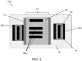
- FIG. 2 shows a top view of an LDMOS, amongst other features, in accordance with additional aspects of the present disclosure.
- several contacts 38a may be formed in contact with the gate structure 21.
- the contacts 38a are parallel to the current flow and in the same plane as the contacts 38 to the source region 32b and the drain region 32a. Further, as shown in this top view, the drain region 32a is farther away from the gate structure 21 than the source region 32.
- the several contacts 38a may be perpendicularly oriented to the several contacts 38.
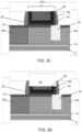
- FIGS. 3A-3F show fabrication processes for manufacturing the gate structure, e.g., FinFET in accordance with aspects of the present disclosure.
- FIG. 3A shows a starting structure comprising a dummy gate 21a formed on the semiconductor substrate 12.
- the semiconductor substrate 12 already includes the wells 14, 16a, 16b and the shallow trench isolation structures 18.
- the wells 14, 16a and 16b may be formed by introducing a concentration of a different dopant of opposite conductivity type in the substrate.
- respective patterned implantation masks may be used to define selected areas exposed for the implantations.
- the implantation masks may include a layer of a light-sensitive material, such as an organic photoresist, applied by a spin coating process, pre-baked, exposed to light projected through a photomask, baked after exposure, and developed with a chemical developer.
- a light-sensitive material such as an organic photoresist
- Each of the implantation masks has a thickness and stopping power sufficient to block masked areas against receiving a dose of the implanted ions.
- the shallow trench isolation structures 18 may be fabricated by conventional lithography, etching and deposition processes.
- a resist is formed over the semiconductor substrate 12 and exposed to energy (light) to form a pattern (opening).
- An etching process with a selective chemistry e.g., reactive ion etching (RIE)
- RIE reactive ion etching
- insulator material e.g., oxide
- CVD chemical vapor deposition
- Any residual insulator material on the surface of the semiconductor substrate 12 can be removed by conventional chemical mechanical polishing (CMP) processes.
- CMP chemical mechanical polishing
- the dummy gate 21a includes sidewall spacers 20 and dummy gate material 40 between the sidewall spacers 20.
- the dummy gate material 40 may be polysilicon deposited by a conventional CVD process, followed by a conventional patterning process, e.g., lithography and etching process. Following the patterning process, sidewall spacer material may be blanket deposited on the patterned dummy gate material 40.
- the sidewall spacer material may be oxide and/or nitride material. Following the blanket deposition of the sidewall spacer material, an anisotropic etching process may be performed to form the sidewall spacers 20.
- the dummy gate material 40 may be removed from between the sidewall spacers 20.
- the dummy gate material 40 may be removed by a conventional selective etching process, e.g., RIE, that removes the polysilicon material.
- the dummy gate material 40 e.g., polysilicon material
- the dummy gate material 40 may be removed by a wet etch or dry etch process.
- the dry etch process may comprise exposing the dummy gate material to a plasma derived from materials that include, but are not limited to, hydrogen chloride (HCl), chlorine (Cl), sulfur hexafluoride (SF 6 ), hydrogen bromide (HBr), and/or hydrogen iodide (HI).
- a hydrogen fluoride (HF) etchant or a conventional wet etchant may be used to remove the dummy gate material.
- these etching processes may be a maskless etching process, using the selective etch chemistry as is known in the art. In this way, a recess 42 may be formed between the sidewall spacers 20.
- the stack of materials 24, 26, 28 may be deposited within the recess 42.
- a high-k dielectric material 24 may be formed over the interfacial layer 22
- a workfunction metal 26 may be formed on the high-k dielectric material 24
- a barrier material 28 may be formed on the workfunction metal 26.
- the barrier material 28 may completely fill any remaining portions of the recess 42.
- the high-k dielectric material 24, workfunction metal 26 and barrier material 28 may be deposited using an ALD process, as an example.
- the high-k dielectric material 24, workfunction metal 26 and barrier material 28 may be etched back to form a recess 44 between the sidewall spacers 20.
- the recess 44 may be below a top surface of the sidewall spacers 20.
- the etch back process may be provided by a conventional RIE process using chemistries that etch or recess the high-k dielectric material 24, workfunction metal 26 and barrier material 28.
- a gate electrode 30 (e.g., tungsten) may be deposited on the barrier material 28, filling the remaining space (e.g., recess) between the sidewall spacers 20.
- the gate electrode 30 may be deposited by a conventional CVD process, followed by a planarization process, e.g., CMP.
- the gate electrode 30 will abut against the sidewall spacers 20 and will extend and be in direct contact with each of the materials 24, 26, 28.
- the volume of tungsten (e.g., gate electrode) between the sidewall spacers 20 is significantly increased compared to conventional gate structures, thus improving Rgate.
- FIG. 3F shows the formation of the drain region 32a, source region 32b and the silicide contacts 34.
- the drain region 32a and the source region 32b may be a raised drain region 32a and a raised source region 32b, fabricated by epitaxial semiconductor growth processes.
- the semiconductor material may be Si or SiGe as examples.
- the epitaxy regions are formed of a III-V compound semiconductor such as GaAs, InP, GaN, InGaAs, InAlAs, GaSb, AlSb, AlAs, A1P, GaP, combinations thereof, or multi-layers thereof.
- the p-type impurity may be in-situ doped.
- An annealing process may be performed to drive in the dopant into the semiconductor substrate 12, e.g., wells 16a, 16b.
- the annealing process may accordingly provide the drain region 32a and the source region 32b deeper into the semiconductor substrate 12.
- the shallow trench isolation structure 18 will provide an additional distance between the drain region 32a and the channel region 23 of the gate structure 21.
- the drain region 32a may be separated from a channel region 23 of the gate structure 21 by the shallow trench isolation structure 18. That is, the shallow trench isolation structure 18 will effectively make the drain region 32a farther from the gate structure 21 than the source region 32b, which is not separated from the gate structure 21 by any shallow trench isolation structure. Accordingly, by having the drain region 32a further away from the from the gate structure 21, it is now possible to also improve gate to drain capacitance (Cgd).
- Cgd gate to drain capacitance
- the silicide contacts 34 may be formed by a silicide process.
- the silicide process begins with deposition of a thin transition metal layer, e.g., nickel, cobalt or titanium, over fully formed and patterned semiconductor devices (e.g., doped or ion implanted source and drain regions). After deposition of the material, the structure is heated allowing the transition metal to react with exposed silicon (or other semiconductor material as described herein) in the active regions of the semiconductor device (e.g., source, drain, gate contact region) forming a low-resistance transition metal silicide. Following the reaction, any remaining transition metal is removed by chemical etching, leaving silicide contacts 34 in the active regions of the device. It should be understood by those of skill in the art that silicide contacts will not be required on metal material, e.g., gate electrode 30. Contacts are formed as noted with respect to FIG. 1 .
- the LDMOS can be utilized in system on chip (SoC) technology.
- SoC is an integrated circuit (also known as a "chip") that integrates all components of an electronic system on a single chip or substrate. As the components are integrated on a single substrate, SoCs consume much less power and take up much less area than multichip designs with equivalent functionality. Because of this, SoCs are becoming the dominant force in the mobile computing (such as in Smartphones) and edge computing markets. SoC is also used in embedded systems and the Internet of Things.
- the method(s) as described above is used in the fabrication of integrated circuit chips.
- the resulting integrated circuit chips can be distributed by the fabricator in raw wafer form (that is, as a single wafer that has multiple unpackaged chips), as a bare die, or in a packaged form.
- the chip is mounted in a single chip package (such as a plastic carrier, with leads that are affixed to a motherboard or other higher level carrier) or in a multichip package (such as a ceramic carrier that has either or both surface interconnections or buried interconnections).
- the chip is then integrated with other chips, discrete circuit elements, and/or other signal processing devices as part of either (a) an intermediate product, such as a motherboard, or (b) an end product.
- the end product can be any product that includes integrated circuit chips, ranging from toys and other low-end applications to advanced computer products having a display, a keyboard or other input device, and a central processor.
- a structure comprising: sidewall spacers over a semiconductor substrate; and a gate structure within a space defined by the sidewall spacers, the gate structure comprising: a plurality of gate materials over the semiconductor substrate and between the sidewall spacers; and a gate electrode over the plurality of gate materials and contacting the sidewall spacers.
- the plurality of gate materials comprises: a gate dielectric material over the semiconductor substrate and between the sidewall spacers; a workfunction metal over the gate dielectric material and between the sidewall spacers; and a barrier material over the workfuction metal and between the sidewall spacers.
- invention 8 or 9 further comprising a shallow trench isolation structure between the drain region and the channel region of the gate structure.
- the gate structure comprises a metal gate structure comprising a channel region below the sidewall spacers and the gate electrode filling an upper space between the sidewall spacers, wherein the structure further comprises a source region adjacent to a first side of the sidewall spacers, a drain region adjacent to a second side of the sidewall spacers and positioned at a distance farther away from the channel region than the source region, and a shallow trench isolation structure between the drain region and the channel region.
- a structure comprising: a metal gate structure comprising a channel region below sidewall spacers and a gate electrode filling an upper space between the sidewall spacers; a source region adjacent to a first side of the sidewall spacers; a drain region adjacent to a second side of the sidewall spacers and positioned at a distance farther away from the channel region than the source region; and a shallow trench isolation structure between the drain region and the channel region.
- the gate structure further comprises a plurality of gate materials under the gate electrode, the plurality of gate materials comprises: a gate dielectric material over a semiconductor substrate and between the sidewall spacers; a workfunction metal over the gate dielectric material and between the sidewall spacers; and a barrier material over the workfuction metal and between the sidewall spacers.
- a method comprising: forming sidewall spacers over a semiconductor substrate; and forming a gate structure within a space defined by the sidewall spacers, the gate structure comprising: forming a plurality of gate materials over the semiconductor substrate and between the sidewall spacers; and forming a gate electrode over the plurality of gate materials and contacting the sidewall spacers.
- the method may form the structure of one of claims 1 to 20.
Landscapes
- Insulated Gate Type Field-Effect Transistor (AREA)
- Engineering & Computer Science (AREA)
- Chemical & Material Sciences (AREA)
- Composite Materials (AREA)
- Materials Engineering (AREA)
- Manufacturing & Machinery (AREA)
Abstract
The present disclosure relates to semiconductor structures and, more particularly, to a laterally diffused metal-oxide semiconductor with one or more gate contacts and methods of manufacture. The structure includes: sidewall spacers over a semiconductor substrate; and a gate structure within a space defined by the sidewall spacers. The gate structure includes: a plurality of gate materials over the semiconductor substrate and between the sidewall spacers; and a gate electrode over the plurality of gate materials and contacting the sidewall spacers.
Description
- The present disclosure relates to semiconductor structures and, more particularly, to a laterally diffused metal-oxide semiconductor with one or more gate contacts and methods of manufacture.
- A laterally-diffused metal-oxide semiconductor (LDMOS) is a planar double-diffused MOSFET (metal-oxide-semiconductor field-effect transistor) used in amplifiers, such as microwave power amplifiers, RF power amplifiers and audio power amplifiers. For example, silicon-based RF LDMOS (radio-frequency LDMOS) is widely used in RF power amplifiers for mobile networks. More specifically, LDMOS devices are widely used in RF power amplifiers for base-stations as the requirement is for high output power with a corresponding drain to source breakdown voltage.
- In an aspect of the disclosure, a structure comprises: sidewall spacers over a semiconductor substrate; and a gate structure within a space defined by the sidewall spacers. The gate structure comprises: a plurality of gate materials over the semiconductor substrate and between the sidewall spacers; and a gate electrode over the plurality of gate materials and contacting the sidewall spacers.
- In an aspect of the disclosure, a structure comprises: a metal gate structure comprising a channel region below sidewall spacers and a gate electrode filling an upper space between the sidewall spacers; a source region adjacent to a first side of the sidewall spacers; a drain region adjacent to a second side of the sidewall spacers and positioned at a distance farther away from the channel region than the source region; and a shallow trench isolation structure between the drain region and the channel region
- In an aspect of the disclosure, a method comprises: forming sidewall spacers over a semiconductor substrate; and a forming a gate structure within a space defined by the sidewall spacers. The gate structure comprises: forming a plurality of gate materials over the semiconductor substrate and between the sidewall spacers; and forming a gate electrode over the plurality of gate materials and contacting the sidewall spacers.
- The present disclosure is described in the detailed description which follows, in reference to the noted plurality of drawings by way of non-limiting examples of exemplary embodiments of the present disclosure.
-
FIG. 1 shows an LDMOS, amongst other features, and respective fabrication processes in accordance with aspects of the present disclosure. -
FIG. 2 shows a top view of an LDMOS, amongst other features, in accordance with additional aspects of the present disclosure. -
FIGS. 3A-3F show fabrication processes for forming a gate structure, e.g., FinFET, in accordance with aspects of the present disclosure. - The present disclosure relates to semiconductor structures and, more particularly, to a laterally diffused metal-oxide semiconductor (LDMOS) with one or more gate contacts and methods of manufacture. More specifically, the present disclosure relates to an LDMOS with an improved gate contact scheme. For example, in embodiments, the LDMOS may be a FinFET P-LDMOS with a gate electrode comprising an increased volume and, hence, exhibiting a lower gate resistance. In further embodiments, the drain region may be farther from the gate structure than the source region, which improves gate to drain capacitance (Cgd). Accordingly, and advantageously, the present disclosure provides RF performance improvement in LDMOS p-FETs, i.e., improved Fmax.
- The LDMOS of the present disclosure can be manufactured in a number of ways using a number of different tools. In general, though, the methodologies and tools are used to form structures with dimensions in the micrometer and nanometer scale. The methodologies, i.e., technologies, employed to manufacture the LDMOS of the present disclosure have been adopted from integrated circuit (IC) technology. For example, the structures are built on wafers and are realized in films of material patterned by photolithographic processes on the top of a wafer. In particular, the fabrication of the LDMOS uses three basic building blocks: (i) deposition of thin films of material on a substrate, (ii) applying a patterned mask on top of the films by photolithographic imaging, and (iii) etching the films selectively to the mask. In addition, precleaning processes may be used to clean etched surfaces of any contaminants, as is known in the art. Moreover, when necessary, rapid thermal anneal processes may be used to drive-in dopants or material layers as is known in the art.
-
FIG. 1 shows an LDMOS, amongst other features, and respective fabrication processes in accordance with aspects of the present disclosure. In particular, the LDMOS 10 includes asemiconductor substrate 12. In embodiments, thesemiconductor substrate 12 may be a P-type substrate composed of any suitable material including, but not limited to, Si, SiGe, SiGeC, SiC, GaAs, InAs, InP, and other III/V or II/VI compound semiconductors. In embodiments, thesemiconductor substrate 12 may be a bulk substrate or, alternatively, may be semiconductor on insulator (SOI) technologies. Thesemiconductor substrate 12 may also comprise any suitable crystallographic orientation (e.g., a (100), (110), (111), or (001) crystallographic orientation). - A deep n-
well 14 may be formed in thesemiconductor substrate 12. A P-well 16a and an N-well 16b may also be formed in thesemiconductor substrate 12. In embodiments, thewells semiconductor substrate 12. The P-well 16a may be doped with p-type dopants, e.g., Boron (B), and the N-wells - Still referring to
FIG. 1 , one or more shallowtrench isolation structures 18 may be formed in thesemiconductor substrate 12. The one or more shallowtrench isolation structures 18 may be formed on a drain side of the device, within the P-well 16a, for example. The one or more shallowtrench isolation structures 18 can be formed by conventional lithography, etching and deposition methods known to those of skill in the art as described in more detail with respect toFIG. 3A . -
Sidewall spacers 20 may be formed on thesemiconductor substrate 12. In embodiments, thesidewall spacers 20 may be formed over the N-well 16b and the P-well 16a, and more particularly partially over the shallowtrench isolation structure 18 that is within the P-well 16a. As described in more detail below with respect toFIG. 3A , thesidewall spacers 20 may be formed using dummy gate fabrication processing schemes. Prior to forming thesidewall spacers 20, aninterfacial layer 22 may be provided on thesemiconductor substrate 12 under thesidewall spacers 20. In embodiments, theinterfacial layer 22 may be an oxide layer, deposited by a conventional deposition method, e.g., atomic layer deposition (ALD), etc. -
FIG. 1 further shows agate structure 21 formed between thesidewall spacers 20, which comprises several layers of stackedmaterials material gate structure 21 may be a FinFET structure. - To form the
gate structure 21, a high-kdielectric material 24 may be formed over theinterfacial layer 22 and between thesidewall spacers 20. In embodiments, the high-k gatedielectric material 24, e.g., HfO2 Al2O3, Ta2O3, TiO2, La2O3, SrTiO3, LaAlO3, ZrO2, Y2O3, Gd2O3, and combinations including multilayers thereof Aworkfunction metal 26 may be formed on the high-kdielectric material 24 and between thesidewall spacers 20. In embodiments, theworkfunction metal 26 may be, e.g., Ti, TiAlC, Al, TiAl, TaN, TaAlC, TiN, TiC and Co. In one embodiment, TiN is used for a p-FET. As shown, each of thematerials material 24 surrounding the bottom and sides of the material 26) due to an etch back process as described with respect toFIG. 3D . - A
barrier material 28 may be formed over theworkfunction metal 26 and between thesidewall spacers 20. In embodiments, thebarrier material 28 may be TaN. Following an etch back process, a gate electrode 30 (e.g., tungsten) may be deposited on thebarrier material 28, filling the remaining space between thesidewall spacers 20, e.g., which abuts (e.g., directly contacts) thesidewall spacers 20. As a result of the etch back process, the volume of tungsten (e.g., gate electrode) between thesidewall spacers 20 is significantly increased, thus improving Rgate. - Still referring to
FIG. 1 , adrain region 32a and asource region 32b may be formed on sides of thegate structure 21. In more specific embodiments, thedrain region 32a and thesource region 32b are abutting thesidewall spacers 20 of thegate structure 21. In embodiments, thedrain region 32a may be farther away from thegate structure 21, e.g.,channel region 23, compared to thesource region 32b due to location of the shallowtrench isolation structure 18. The location of thedrain region 32a will lower the drain to gate capacitance (Cgd). - In embodiments, the
drain region 32a and thesource region 32b may be a raiseddrain region 32a and a raisedsource region 32b, fabricated by conventional epitaxial semiconductor growth processes as is known in the art and as described in more detail with respect toFIG. 3F . Also, as described in more detail with respect toFIG. 3F , asilicide contact 34 may be formed on the raiseddrain region 32a and the raisedsource region 32b. In embodiments, thesilicide contact 34 may be, e.g., NiSi or TiSi. -
Contacts 38 may be formed to thesilicide contacts 34 and the gate structure 21 (the contact to the gate structure is not shown inFIG. 1 ). To form thecontacts 38, an interlevel dielectric material 36 may be formed over the structure, which is then subjected to a lithography and etching process to form trenches exposing thesilicide contacts 34 and thegate structure 21. A conductive material, e.g., aluminum with a liner material such as TiN, may be deposited within the trenches to form thecontacts 38. Any residual material formed on a top surface of the interlevel dielectric material 36 may be removed by a conventional CMP process. -
FIG. 2 shows a top view of an LDMOS, amongst other features, in accordance with additional aspects of the present disclosure. In thestructure 10a,several contacts 38a may be formed in contact with thegate structure 21. In embodiments, thecontacts 38a are parallel to the current flow and in the same plane as thecontacts 38 to thesource region 32b and thedrain region 32a. Further, as shown in this top view, thedrain region 32a is farther away from thegate structure 21 than the source region 32. Theseveral contacts 38a may be perpendicularly oriented to theseveral contacts 38. -
FIGS. 3A-3F show fabrication processes for manufacturing the gate structure, e.g., FinFET in accordance with aspects of the present disclosure.FIG. 3A shows a starting structure comprising adummy gate 21a formed on thesemiconductor substrate 12. In this structure, thesemiconductor substrate 12 already includes thewells trench isolation structures 18. Thewells - The shallow
trench isolation structures 18 may be fabricated by conventional lithography, etching and deposition processes. For example, a resist is formed over thesemiconductor substrate 12 and exposed to energy (light) to form a pattern (opening). An etching process with a selective chemistry, e.g., reactive ion etching (RIE), will be used to transfer the pattern to thesemiconductor substrate 12 to form one or more trenches in thesemiconductor substrate 12 through the openings of the resist. Following the resist removal by a conventional oxygen ashing process or other known stripants, insulator material, e.g., oxide, can be deposited by any conventional deposition process, e.g., chemical vapor deposition (CVD) process. Any residual insulator material on the surface of thesemiconductor substrate 12 can be removed by conventional chemical mechanical polishing (CMP) processes. - Still referring to
FIG. 3A , thedummy gate 21a includessidewall spacers 20 anddummy gate material 40 between thesidewall spacers 20. In embodiments, thedummy gate material 40 may be polysilicon deposited by a conventional CVD process, followed by a conventional patterning process, e.g., lithography and etching process. Following the patterning process, sidewall spacer material may be blanket deposited on the patterneddummy gate material 40. The sidewall spacer material may be oxide and/or nitride material. Following the blanket deposition of the sidewall spacer material, an anisotropic etching process may be performed to form thesidewall spacers 20. - In
FIG. 3B , the dummy gate material 40 (e.g., polysilicon material) may be removed from between thesidewall spacers 20. For example, thedummy gate material 40 may be removed by a conventional selective etching process, e.g., RIE, that removes the polysilicon material. By way of an illustrative and non-limiting example, the dummy gate material 40 (e.g., polysilicon material) may be removed by a wet etch or dry etch process. The dry etch process may comprise exposing the dummy gate material to a plasma derived from materials that include, but are not limited to, hydrogen chloride (HCl), chlorine (Cl), sulfur hexafluoride (SF6), hydrogen bromide (HBr), and/or hydrogen iodide (HI). In one embodiment, a hydrogen fluoride (HF) etchant or a conventional wet etchant may be used to remove the dummy gate material. In embodiments, these etching processes may be a maskless etching process, using the selective etch chemistry as is known in the art. In this way, arecess 42 may be formed between thesidewall spacers 20. - As shown in
FIG. 3C , the stack ofmaterials recess 42. For example, a high-k dielectric material 24 may be formed over theinterfacial layer 22, aworkfunction metal 26 may be formed on the high-k dielectric material 24, and abarrier material 28 may be formed on theworkfunction metal 26. In embodiments, thebarrier material 28 may completely fill any remaining portions of therecess 42. The high-k dielectric material 24,workfunction metal 26 andbarrier material 28 may be deposited using an ALD process, as an example. - In
FIG. 3D , the high-k dielectric material 24,workfunction metal 26 andbarrier material 28 may be etched back to form arecess 44 between thesidewall spacers 20. In embodiments, therecess 44 may be below a top surface of thesidewall spacers 20. Also, in embodiments, the etch back process may be provided by a conventional RIE process using chemistries that etch or recess the high-k dielectric material 24,workfunction metal 26 andbarrier material 28. - In
FIG. 3E , following the etch back process, a gate electrode 30 (e.g., tungsten) may be deposited on thebarrier material 28, filling the remaining space (e.g., recess) between thesidewall spacers 20. In embodiments, thegate electrode 30 may be deposited by a conventional CVD process, followed by a planarization process, e.g., CMP. Thegate electrode 30 will abut against thesidewall spacers 20 and will extend and be in direct contact with each of thematerials sidewall spacers 20 is significantly increased compared to conventional gate structures, thus improving Rgate. -
FIG. 3F shows the formation of thedrain region 32a,source region 32b and thesilicide contacts 34. In embodiments, thedrain region 32a and thesource region 32b may be a raiseddrain region 32a and a raisedsource region 32b, fabricated by epitaxial semiconductor growth processes. In embodiments, the semiconductor material may be Si or SiGe as examples. In accordance with alternative, the epitaxy regions are formed of a III-V compound semiconductor such as GaAs, InP, GaN, InGaAs, InAlAs, GaSb, AlSb, AlAs, A1P, GaP, combinations thereof, or multi-layers thereof. Also, in a p-type FinFET implementation, the p-type impurity may be in-situ doped. An annealing process may be performed to drive in the dopant into thesemiconductor substrate 12, e.g.,wells drain region 32a and thesource region 32b deeper into thesemiconductor substrate 12. The shallowtrench isolation structure 18 will provide an additional distance between thedrain region 32a and thechannel region 23 of thegate structure 21. - The
drain region 32a may be separated from achannel region 23 of thegate structure 21 by the shallowtrench isolation structure 18. That is, the shallowtrench isolation structure 18 will effectively make thedrain region 32a farther from thegate structure 21 than thesource region 32b, which is not separated from thegate structure 21 by any shallow trench isolation structure. Accordingly, by having thedrain region 32a further away from the from thegate structure 21, it is now possible to also improve gate to drain capacitance (Cgd). - The
silicide contacts 34 may be formed by a silicide process. The silicide process begins with deposition of a thin transition metal layer, e.g., nickel, cobalt or titanium, over fully formed and patterned semiconductor devices (e.g., doped or ion implanted source and drain regions). After deposition of the material, the structure is heated allowing the transition metal to react with exposed silicon (or other semiconductor material as described herein) in the active regions of the semiconductor device (e.g., source, drain, gate contact region) forming a low-resistance transition metal silicide. Following the reaction, any remaining transition metal is removed by chemical etching, leavingsilicide contacts 34 in the active regions of the device. It should be understood by those of skill in the art that silicide contacts will not be required on metal material, e.g.,gate electrode 30. Contacts are formed as noted with respect toFIG. 1 . - The LDMOS can be utilized in system on chip (SoC) technology. The SoC is an integrated circuit (also known as a "chip") that integrates all components of an electronic system on a single chip or substrate. As the components are integrated on a single substrate, SoCs consume much less power and take up much less area than multichip designs with equivalent functionality. Because of this, SoCs are becoming the dominant force in the mobile computing (such as in Smartphones) and edge computing markets. SoC is also used in embedded systems and the Internet of Things.
- The method(s) as described above is used in the fabrication of integrated circuit chips. The resulting integrated circuit chips can be distributed by the fabricator in raw wafer form (that is, as a single wafer that has multiple unpackaged chips), as a bare die, or in a packaged form. In the latter case the chip is mounted in a single chip package (such as a plastic carrier, with leads that are affixed to a motherboard or other higher level carrier) or in a multichip package (such as a ceramic carrier that has either or both surface interconnections or buried interconnections). In any case the chip is then integrated with other chips, discrete circuit elements, and/or other signal processing devices as part of either (a) an intermediate product, such as a motherboard, or (b) an end product. The end product can be any product that includes integrated circuit chips, ranging from toys and other low-end applications to advanced computer products having a display, a keyboard or other input device, and a central processor.
- The descriptions of the various embodiments of the present disclosure have been presented for purposes of illustration, but are not intended to be exhaustive or limited to the embodiments disclosed. Many modifications and variations will be apparent to those of ordinary skill in the art without departing from the scope and spirit of the described embodiments. The terminology used herein was chosen to best explain the principles of the embodiments, the practical application or technical improvement over technologies found in the marketplace, or to enable others of ordinary skill in the art to understand the embodiments disclosed herein.
- The following embodiments are explicitly disclosed:
- A structure comprising: sidewall spacers over a semiconductor substrate; and
a gate structure within a space defined by the sidewall spacers, the gate structure comprising: a plurality of gate materials over the semiconductor substrate and between the sidewall spacers; and a gate electrode over the plurality of gate materials and contacting the sidewall spacers. - The structure of embodiment 1, wherein the plurality of gate materials comprises:
a gate dielectric material over the semiconductor substrate and between the sidewall spacers; a workfunction metal over the gate dielectric material and between the sidewall spacers; and a barrier material over the workfuction metal and between the sidewall spacers. - The structure of embodiment 2, wherein the gate dielectric material comprises a high-k gate dielectric material.
- The structure of embodiment 2 or 3, wherein the workfunction material and the gate dielectric material comprise a U-shape.
- The structure of one of embodiments 2 to 4, wherein the gate electrode further contacts the gate dielectric material, the workfunction material and the barrier material.
- The structure of one of embodiments 2 to 5, wherein the gate dielectric material, the workfunction metal and the barrier material partly fill a space between the sidewall spacers and the gate electrode completely fills a remainder of the space between the sidewall spacers.
- The structure of one of embodiments 1 to 6, wherein the gate electrode comprises tungsten.
- The structure of one of embodiments 1 to 7, further comprising a source region and a drain region on opposing sides of the sidewall spacers.
- The structure of embodiment 8, wherein the drain region is farther away from a channel region of the gate structure than the source region.
- The structure of embodiment 8 or 9, further comprising a shallow trench isolation structure between the drain region and the channel region of the gate structure.
- The structure of one of embodiments 8 to 10, further comprising a plurality of contacts to the gate electrode, which are oriented in a direction of current flow and in a same plane as contacts to the source region and the drain region.
- The structure of one of embodiments 8 to 11, wherein the gate structure comprises a metal gate structure comprising a channel region below the sidewall spacers and the gate electrode filling an upper space between the sidewall spacers, wherein the structure further comprises a source region adjacent to a first side of the sidewall spacers, a drain region adjacent to a second side of the sidewall spacers and positioned at a distance farther away from the channel region than the source region, and a shallow trench isolation structure between the drain region and the channel region.
- A structure comprising:
a metal gate structure comprising a channel region below sidewall spacers and a gate electrode filling an upper space between the sidewall spacers; a source region adjacent to a first side of the sidewall spacers; a drain region adjacent to a second side of the sidewall spacers and positioned at a distance farther away from the channel region than the source region; and a shallow trench isolation structure between the drain region and the channel region. - The structure of
embodiment 12 or 13, wherein the gate structure further comprises a plurality of gate materials under the gate electrode, the plurality of gate materials comprises: a gate dielectric material over a semiconductor substrate and between the sidewall spacers; a workfunction metal over the gate dielectric material and between the sidewall spacers; and a barrier material over the workfuction metal and between the sidewall spacers. - The structure of one of
embodiments 12 to 14, wherein the gate dielectric material comprises a high-k dielectric material. - The structure of one of
embodiments 12 to 15, wherein the gate electrode contacts the gate dielectric material, the workfunction material and the barrier material. - The structure of one of
embodiments 12 to 16, wherein the gate dielectric material, the workfunction metal and the barrier material completely fill a space between the sidewall spacers underneath the gate electrode and the gate electrode completely fills a remainder of the space between the sidewall spacers. - The structure of one of
embodiments 12 to 17, wherein the source region and the drain region are a raised source region and a raised drain region. - The structure of one of
embodiments 12 to 18, wherein the gate electrode comprises tungsten. - The structure of one of
embodiments 12 to 19, further comprising a plurality of contacts to the gate electrode, which are oriented in a direction of current flow and in a same plane as contacts to the source region and the drain region. - A method comprising: forming sidewall spacers over a semiconductor substrate; and forming a gate structure within a space defined by the sidewall spacers, the gate structure comprising: forming a plurality of gate materials over the semiconductor substrate and between the sidewall spacers; and forming a gate electrode over the plurality of gate materials and contacting the sidewall spacers. The method may form the structure of one of claims 1 to 20.
Claims (15)
- A structure comprising:sidewall spacers over a semiconductor substrate; anda gate structure within a space defined by the sidewall spacers, the gate structure comprising:a plurality of gate materials over the semiconductor substrate and between the sidewall spacers; anda gate electrode over the plurality of gate materials and contacting the sidewall spacers.
- The structure of claim 1, wherein the plurality of gate materials comprises:a gate dielectric material over the semiconductor substrate and between the sidewall spacers;a workfunction metal over the gate dielectric material and between the sidewall spacers; anda barrier material over the workfuction metal and between the sidewall spacers.
- The structure of claim 2, wherein the gate dielectric material comprises a high-k gate dielectric material.
- The structure of claim 2 or 3, wherein the workfunction material and the gate dielectric material comprise a U-shape, and/or wherein the gate electrode further contacts the gate dielectric material, the workfunction material and the barrier material.
- The structure of one of claims 2 to 4, wherein the gate dielectric material, the workfunction metal and the barrier material partly fill a space between the sidewall spacers and the gate electrode completely fills a remainder of the space between the sidewall spacers.
- The structure of one of claims 1 to 5, further comprising a source region and a drain region on opposing sides of the sidewall spacers.
- The structure of claim 6, wherein the structure further comprises a plurality of contacts to the gate electrode, which are oriented in a direction of current flow and in a same plane as contacts to the source region and the drain region, and/or a shallow trench isolation structure between the drain region and the channel region of the gate structure, and/or wherein the drain region is farther away from a channel region of the gate structure than the source region.
- The structure of one of claims 1 to 7, wherein the gate structure comprises a metal gate structure comprising a channel region below the sidewall spacers and the gate electrode filling an upper space between the sidewall spacers, wherein the structure further comprises a source region adjacent to a first side of the sidewall spacers, a drain region adjacent to a second side of the sidewall spacers and positioned at a distance farther away from the channel region than the source region, and a shallow trench isolation structure between the drain region and the channel region.
- The structure of claim 8, wherein the plurality of gate materials is under the gate electrode.
- The structure of claim 8 or 9, wherein the gate dielectric material, the workfunction metal and the barrier material completely fill a space between the sidewall spacers underneath the gate electrode and the gate electrode completely fills a remainder of the space between the sidewall spacers.
- The structure of one of claims 8 to 10, wherein the source region and the drain region are a raised source region and a raised drain region.
- The structure of one of claims 8 to 11, further comprising a plurality of contacts to the gate electrode, which are oriented in a direction of current flow and in a same plane as contacts to the source region and the drain region.
- The structure of one of claims 1 to 12, wherein the gate electrode comprises tungsten.
- A method comprising:forming sidewall spacers over a semiconductor substrate; andforming a gate structure within a space defined by the sidewall spacers, the gate structure comprising:forming a plurality of gate materials over the semiconductor substrate and between the sidewall spacers; andforming a gate electrode over the plurality of gate materials and contacting the sidewall spacers.
- The method of claim 14, wherein the structure of one of claims 1 to 13 is formed.
Applications Claiming Priority (1)
| Application Number | Priority Date | Filing Date | Title |
|---|---|---|---|
| US17/708,698 US12324217B2 (en) | 2022-03-30 | 2022-03-30 | Laterally diffused metal-oxide semiconductor with gate contact |
Publications (1)
| Publication Number | Publication Date |
|---|---|
| EP4254510A1 true EP4254510A1 (en) | 2023-10-04 |
Family
ID=84044066
Family Applications (1)
| Application Number | Title | Priority Date | Filing Date |
|---|---|---|---|
| EP22200196.8A Pending EP4254510A1 (en) | 2022-03-30 | 2022-10-07 | Laterally diffused metal-oxide semiconductor with gate contact |
Country Status (2)
| Country | Link |
|---|---|
| US (1) | US12324217B2 (en) |
| EP (1) | EP4254510A1 (en) |
Citations (4)
| Publication number | Priority date | Publication date | Assignee | Title |
|---|---|---|---|---|
| US9450074B1 (en) * | 2011-07-29 | 2016-09-20 | Maxim Integrated Products, Inc. | LDMOS with field plate connected to gate |
| US9577078B1 (en) * | 2015-09-25 | 2017-02-21 | Taiwan Semiconductor Manufacturing Co., Ltd. | Structure and formation method of semiconductor device structure |
| US20170365602A1 (en) * | 2016-06-15 | 2017-12-21 | Semiconductor Manufacturing International (Shanghai) Corporation | Ldmos design for a finfet device |
| US20190348517A1 (en) * | 2018-05-08 | 2019-11-14 | Globalfoundries Inc. | Chamfered replacement gate structures |
Family Cites Families (11)
| Publication number | Priority date | Publication date | Assignee | Title |
|---|---|---|---|---|
| US9461143B2 (en) | 2012-09-19 | 2016-10-04 | Intel Corporation | Gate contact structure over active gate and method to fabricate same |
| US9418993B2 (en) | 2013-08-05 | 2016-08-16 | Globalfoundries Inc. | Device and method for a LDMOS design for a FinFET integrated circuit |
| US9905671B2 (en) | 2015-08-19 | 2018-02-27 | International Business Machines Corporation | Forming a gate contact in the active area |
| KR20180102273A (en) | 2017-03-07 | 2018-09-17 | 삼성전자주식회사 | Semiconductor device and method for fabricating the same |
| US10084053B1 (en) * | 2017-03-27 | 2018-09-25 | Globalfoundries Inc. | Gate cuts after metal gate formation |
| US10283623B2 (en) | 2017-07-27 | 2019-05-07 | Taiwan Semiconductor Manufacturing Co., Ltd. | Integrated circuits with gate stacks |
| US11742404B2 (en) * | 2020-04-29 | 2023-08-29 | Taiwan Semiconductor Manufacturing Co., Ltd. | Method of manufacturing a semiconductor device and a semiconductor device |
| US20210351293A1 (en) * | 2020-05-08 | 2021-11-11 | Globalfoundries U.S. Inc. | Novel gate structure for an ldmos transistor device |
| US20210407935A1 (en) | 2020-06-30 | 2021-12-30 | GLOBALFOUNDRIES U.S.Inc. | Semiconductor transistors suitable for radio-frequency applications |
| US11342453B2 (en) * | 2020-08-18 | 2022-05-24 | Globalfoundries U.S. Inc. | Field effect transistor with asymmetric gate structure and method |
| US12660234B2 (en) | 2023-02-21 | 2026-06-16 | Globalfoundries U.S. Inc | Device with workfunction metal in drift region |
-
2022
- 2022-03-30 US US17/708,698 patent/US12324217B2/en active Active
- 2022-10-07 EP EP22200196.8A patent/EP4254510A1/en active Pending
Patent Citations (4)
| Publication number | Priority date | Publication date | Assignee | Title |
|---|---|---|---|---|
| US9450074B1 (en) * | 2011-07-29 | 2016-09-20 | Maxim Integrated Products, Inc. | LDMOS with field plate connected to gate |
| US9577078B1 (en) * | 2015-09-25 | 2017-02-21 | Taiwan Semiconductor Manufacturing Co., Ltd. | Structure and formation method of semiconductor device structure |
| US20170365602A1 (en) * | 2016-06-15 | 2017-12-21 | Semiconductor Manufacturing International (Shanghai) Corporation | Ldmos design for a finfet device |
| US20190348517A1 (en) * | 2018-05-08 | 2019-11-14 | Globalfoundries Inc. | Chamfered replacement gate structures |
Also Published As
| Publication number | Publication date |
|---|---|
| US12324217B2 (en) | 2025-06-03 |
| US20230317815A1 (en) | 2023-10-05 |
Similar Documents
| Publication | Publication Date | Title |
|---|---|---|
| US20070026590A1 (en) | Dynamic Schottky barrier MOSFET device and method of manufacture | |
| US20240162345A1 (en) | Transistor with metal field plate contact | |
| US20050087824A1 (en) | High performance fet with laterally thin extension | |
| US11749717B2 (en) | Transistor with embedded isolation layer in bulk substrate | |
| US11798948B2 (en) | Semiconductor structure with shared well | |
| EP4421873A1 (en) | Device with workfunction metal in drift region | |
| US10121878B1 (en) | LDMOS finFET structures with multiple gate structures | |
| EP4401123A1 (en) | Device with isolation structures in active regions | |
| US20240030341A1 (en) | High performance laterally-diffused metal-oxide semiconductor structure | |
| US20240282852A1 (en) | Semiconductor structure with device including at least one in-well porous region | |
| US12408373B1 (en) | Device with three dimensional channel | |
| US12289913B1 (en) | Device with metal field plate extension | |
| US20230062747A1 (en) | Lateral bipolar transistor | |
| US11705455B2 (en) | High voltage extended drain MOSFET (EDMOS) devices in a high-k metal gate (HKMG) | |
| US20240363741A1 (en) | Lateral bipolar transistors | |
| US11239315B2 (en) | Dual trench isolation structures | |
| US20250089317A1 (en) | Nanosheet structures with bottom semiconductor material | |
| US12324217B2 (en) | Laterally diffused metal-oxide semiconductor with gate contact | |
| US10170617B2 (en) | Vertical transport field effect transistors | |
| US11289598B2 (en) | Co-integrated high voltage (HV) and medium voltage (MV) field effect transistors | |
| US20240395932A1 (en) | Wraparound gate structure | |
| US20260123005A1 (en) | Transistor with field plate | |
| US20260068279A1 (en) | Extended drain metal oxide semiconductor device | |
| EP4496005A1 (en) | Nanosheet structures with corner spacer | |
| US12349444B1 (en) | Under-source body contact |
Legal Events
| Date | Code | Title | Description |
|---|---|---|---|
| PUAI | Public reference made under article 153(3) epc to a published international application that has entered the european phase |
Free format text: ORIGINAL CODE: 0009012 |
|
| STAA | Information on the status of an ep patent application or granted ep patent |
Free format text: STATUS: REQUEST FOR EXAMINATION WAS MADE |
|
| 17P | Request for examination filed |
Effective date: 20221007 |
|
| AK | Designated contracting states |
Kind code of ref document: A1 Designated state(s): AL AT BE BG CH CY CZ DE DK EE ES FI FR GB GR HR HU IE IS IT LI LT LU LV MC ME MK MT NL NO PL PT RO RS SE SI SK SM TR |