EP4254505A1 - Field-effect transistors having a gate electrode positioned inside a substrate recess - Google Patents
Field-effect transistors having a gate electrode positioned inside a substrate recess Download PDFInfo
- Publication number
- EP4254505A1 EP4254505A1 EP22198020.4A EP22198020A EP4254505A1 EP 4254505 A1 EP4254505 A1 EP 4254505A1 EP 22198020 A EP22198020 A EP 22198020A EP 4254505 A1 EP4254505 A1 EP 4254505A1
- Authority
- EP
- European Patent Office
- Prior art keywords
- recess
- semiconductor substrate
- dielectric layer
- width
- gate electrode
- Prior art date
- Legal status (The legal status is an assumption and is not a legal conclusion. Google has not performed a legal analysis and makes no representation as to the accuracy of the status listed.)
- Pending
Links
Images


Classifications
-
- H—ELECTRICITY
- H10—SEMICONDUCTOR DEVICES; ELECTRIC SOLID-STATE DEVICES NOT OTHERWISE PROVIDED FOR
- H10D—INORGANIC ELECTRIC SEMICONDUCTOR DEVICES
- H10D64/00—Electrodes of devices having potential barriers
- H10D64/01—Manufacture or treatment
- H10D64/025—Manufacture or treatment forming recessed gates, e.g. by using local oxidation
-
- H—ELECTRICITY
- H10—SEMICONDUCTOR DEVICES; ELECTRIC SOLID-STATE DEVICES NOT OTHERWISE PROVIDED FOR
- H10D—INORGANIC ELECTRIC SEMICONDUCTOR DEVICES
- H10D62/00—Semiconductor bodies, or regions thereof, of devices having potential barriers
- H10D62/10—Shapes, relative sizes or dispositions of the regions of the semiconductor bodies; Shapes of the semiconductor bodies
- H10D62/113—Isolations within a component, i.e. internal isolations
- H10D62/115—Dielectric isolations, e.g. air gaps
-
- H—ELECTRICITY
- H10—SEMICONDUCTOR DEVICES; ELECTRIC SOLID-STATE DEVICES NOT OTHERWISE PROVIDED FOR
- H10D—INORGANIC ELECTRIC SEMICONDUCTOR DEVICES
- H10D30/00—Field-effect transistors [FET]
- H10D30/01—Manufacture or treatment
- H10D30/021—Manufacture or treatment of FETs having insulated gates [IGFET]
- H10D30/0221—Manufacture or treatment of FETs having insulated gates [IGFET] having asymmetry in the channel direction, e.g. lateral high-voltage MISFETs having drain offset region or extended-drain MOSFETs [EDMOS]
-
- H—ELECTRICITY
- H10—SEMICONDUCTOR DEVICES; ELECTRIC SOLID-STATE DEVICES NOT OTHERWISE PROVIDED FOR
- H10D—INORGANIC ELECTRIC SEMICONDUCTOR DEVICES
- H10D30/00—Field-effect transistors [FET]
- H10D30/60—Insulated-gate field-effect transistors [IGFET]
- H10D30/601—Insulated-gate field-effect transistors [IGFET] having lightly-doped drain or source extensions, e.g. LDD IGFETs or DDD IGFETs
- H10D30/608—Insulated-gate field-effect transistors [IGFET] having lightly-doped drain or source extensions, e.g. LDD IGFETs or DDD IGFETs having non-planar bodies, e.g. having recessed gate electrodes
-
- H—ELECTRICITY
- H10—SEMICONDUCTOR DEVICES; ELECTRIC SOLID-STATE DEVICES NOT OTHERWISE PROVIDED FOR
- H10D—INORGANIC ELECTRIC SEMICONDUCTOR DEVICES
- H10D62/00—Semiconductor bodies, or regions thereof, of devices having potential barriers
- H10D62/10—Shapes, relative sizes or dispositions of the regions of the semiconductor bodies; Shapes of the semiconductor bodies
- H10D62/17—Semiconductor regions connected to electrodes not carrying current to be rectified, amplified or switched, e.g. channel regions
- H10D62/213—Channel regions of field-effect devices
- H10D62/221—Channel regions of field-effect devices of FETs
- H10D62/235—Channel regions of field-effect devices of FETs of IGFETs
- H10D62/292—Non-planar channels of IGFETs
-
- H—ELECTRICITY
- H10—SEMICONDUCTOR DEVICES; ELECTRIC SOLID-STATE DEVICES NOT OTHERWISE PROVIDED FOR
- H10D—INORGANIC ELECTRIC SEMICONDUCTOR DEVICES
- H10D62/00—Semiconductor bodies, or regions thereof, of devices having potential barriers
- H10D62/10—Shapes, relative sizes or dispositions of the regions of the semiconductor bodies; Shapes of the semiconductor bodies
- H10D62/17—Semiconductor regions connected to electrodes not carrying current to be rectified, amplified or switched, e.g. channel regions
- H10D62/351—Substrate regions of field-effect devices
- H10D62/357—Substrate regions of field-effect devices of FETs
- H10D62/364—Substrate regions of field-effect devices of FETs of IGFETs
- H10D62/371—Inactive supplementary semiconductor regions, e.g. for preventing punch-through, improving capacity effect or leakage current
-
- H—ELECTRICITY
- H10—SEMICONDUCTOR DEVICES; ELECTRIC SOLID-STATE DEVICES NOT OTHERWISE PROVIDED FOR
- H10D—INORGANIC ELECTRIC SEMICONDUCTOR DEVICES
- H10D62/00—Semiconductor bodies, or regions thereof, of devices having potential barriers
- H10D62/10—Shapes, relative sizes or dispositions of the regions of the semiconductor bodies; Shapes of the semiconductor bodies
- H10D62/17—Semiconductor regions connected to electrodes not carrying current to be rectified, amplified or switched, e.g. channel regions
- H10D62/351—Substrate regions of field-effect devices
- H10D62/357—Substrate regions of field-effect devices of FETs
- H10D62/364—Substrate regions of field-effect devices of FETs of IGFETs
- H10D62/378—Contact regions to the substrate regions
-
- H—ELECTRICITY
- H10—SEMICONDUCTOR DEVICES; ELECTRIC SOLID-STATE DEVICES NOT OTHERWISE PROVIDED FOR
- H10D—INORGANIC ELECTRIC SEMICONDUCTOR DEVICES
- H10D64/00—Electrodes of devices having potential barriers
- H10D64/20—Electrodes characterised by their shapes, relative sizes or dispositions
- H10D64/27—Electrodes not carrying the current to be rectified, amplified, oscillated or switched, e.g. gates
- H10D64/311—Gate electrodes for field-effect devices
- H10D64/411—Gate electrodes for field-effect devices for FETs
- H10D64/511—Gate electrodes for field-effect devices for FETs for IGFETs
- H10D64/512—Disposition of the gate electrodes, e.g. buried gates
- H10D64/513—Disposition of the gate electrodes, e.g. buried gates within recesses in the substrate, e.g. trench gates, groove gates or buried gates
-
- H—ELECTRICITY
- H10—SEMICONDUCTOR DEVICES; ELECTRIC SOLID-STATE DEVICES NOT OTHERWISE PROVIDED FOR
- H10D—INORGANIC ELECTRIC SEMICONDUCTOR DEVICES
- H10D64/00—Electrodes of devices having potential barriers
- H10D64/20—Electrodes characterised by their shapes, relative sizes or dispositions
- H10D64/27—Electrodes not carrying the current to be rectified, amplified, oscillated or switched, e.g. gates
- H10D64/311—Gate electrodes for field-effect devices
- H10D64/411—Gate electrodes for field-effect devices for FETs
- H10D64/511—Gate electrodes for field-effect devices for FETs for IGFETs
- H10D64/514—Gate electrodes for field-effect devices for FETs for IGFETs characterised by the insulating layers
- H10D64/516—Gate electrodes for field-effect devices for FETs for IGFETs characterised by the insulating layers the thicknesses being non-uniform
-
- H—ELECTRICITY
- H10—SEMICONDUCTOR DEVICES; ELECTRIC SOLID-STATE DEVICES NOT OTHERWISE PROVIDED FOR
- H10D—INORGANIC ELECTRIC SEMICONDUCTOR DEVICES
- H10D62/00—Semiconductor bodies, or regions thereof, of devices having potential barriers
- H10D62/40—Crystalline structures
Definitions
- the disclosure relates to semiconductor device fabrication and integrated circuits and, more specifically, to structures for a field-effect transistor and methods of forming a structure for a field-effect transistor.
- CMOS Complementary-metal-oxide-semiconductor
- a field-effect transistor generally includes a source, a drain, a semiconductor body supplying a channel region between the source and drain, and a gate electrode overlapped with the channel region.
- a control voltage exceeding a characteristic threshold voltage is applied to the gate electrode, carrier flow occurs in the channel region between the source and drain to produce a device output current.
- Conventional field-effect transistors may exhibit an undesirably high value of off-capacitance, which may be detrimental to device performance.
- a structure comprises a semiconductor substrate including a first surface, a recess in the first surface, and a second surface inside the first recess.
- the structure further comprises a shallow trench isolation region extending from the first surface into the semiconductor substrate.
- the shallow trench isolation region is positioned to surround an active device region including the recess.
- a field-effect transistor includes a gate electrode positioned on a portion of the second surface.
- a method comprises forming a recess in a first surface of a semiconductor substrate.
- the semiconductor substrate includes a second surface inside the recess.
- the method further comprises forming a shallow trench isolation region extending from the first surface into the semiconductor substrate.
- the shallow trench isolation region is positioned to surround an active device region including the recess.
- the method further comprises forming a field-effect transistor including a gate electrode positioned on a portion of the second surface.
- a semiconductor substrate 10 that contains a semiconductor material, such as single-crystal silicon.
- a shallow trench isolation region 14 may be formed by a shallow trench isolation technique that patterns trenches in the semiconductor substrate 10 with lithography and etching processes, deposits a dielectric material to overfill the trenches, and planarizes the dielectric material using chemical mechanical polishing and/or an etch back to remove excess dielectric material over a top surface 12 of the semiconductor substrate 10.
- the dielectric material contained in the shallow trench isolation region 14 may be comprised of an electrical insulator, such as silicon dioxide, deposited by chemical vapor deposition.
- the shallow trench isolation region 14 surrounds an active device region 15 of the semiconductor substrate 10 in which a device structure may be subsequently fabricated.
- a high-resistivity layer 16 is positioned in the semiconductor substrate 10 beneath the active device region 15.
- the electrical resistivity of the high-resistivity layer 16 is significantly greater than the electrical resistivity of the semiconductor substrate 10 in the active device region 15 or the bulk portion of the semiconductor substrate 10 that surrounds the active device region 15.
- the high-resistivity layer 16 may be comprised of a polycrystalline semiconductor material, such as polysilicon, formed in the semiconductor substrate 10 by an amorphizing ion implantation and a subsequent anneal that recrystallizes the amorphous semiconductor material of the semiconductor substrate 10.
- the high-resistivity layer 16 may abut the shallow trench isolation region 14 and, in particular, the high-resistivity layer 16 may abut a lowermost portion of the shallow trench isolation region 14 such that the active device region 15 is fully isolated from the bulk portion of the semiconductor substrate 10, which may improve device performance for a device structure subsequently fabricated in the active device region 15.
- Dielectric layers 18, 20 may be formed and patterned by lithography and etching processes to define an opening 21 that extends to a portion of the top surface 12 of the semiconductor substrate 10 in the active device region 15.
- the dielectric layer 18 may be comprised of a dielectric material, such as silicon dioxide, grown by thermal oxidation.
- the dielectric layer 20 may be comprised of a dielectric material, such as silicon nitride, deposited by chemical vapor deposition.
- the opening 21 in the dielectric layers 18, 20 may be arranged over a centrally-located area of the top surface 12 of the semiconductor substrate 10 in the active device region 15.
- a dielectric layer 22 is formed at the location of the opening 21 in the dielectric layers 18, 20.
- the dielectric layer 22 may be comprised of a dielectric material, such as silicon dioxide.
- the dielectric layer 22 may be comprised of silicon dioxide formed by subjecting the portion of the semiconductor substrate 10 at the location of the opening 21 to thermal oxidation in an oxidizing atmosphere (e.g., an atmosphere with an oxygen content) using a local oxidation of silicon (LOCOS) process.
- an oxidizing atmosphere e.g., an atmosphere with an oxygen content
- the oxidizing species e.g., oxygen
- the oxidizing species is barred from diffusing through the thickness of the dielectric layer 20 during thermal oxidation, and the opening 21 in the dielectric layer 20 exposes an unprotected portion of the semiconductor substrate 10 that is thermally oxidized to grow the dielectric layer 22.
- the oxidizing species laterally diffuses in the semiconductor substrate 10 beneath the dielectric layer 20 at the side edges of the opening 21 and oxidizes the semiconductor material under the side edges.
- the dielectric layer 22 tapers from a full thickness interior of the side edges of the opening 21 to a near-zero thickness beneath the dielectric layer 20, and the dielectric layer 22 is faceted adjacent to the side edges of the opening 21 in the dielectric layer 20.
- the formation of the dielectric layer 22 may cause the dielectric layer 20 proximate to the side edges of the opening 21 to be deflected upwardly.
- the dielectric layers 18, 20 and the dielectric layer 22 are removed by one or more etching processes.
- the removal of the dielectric layer 22 generates a faceted recess 24 in the top surface 12 of the semiconductor substrate 10.
- the shape and dimensions of the faceted recess 24 are defined by the shape and dimensions of the removed dielectric layer 22.
- the shallow trench isolation region 14 is positioned to surround the portion of the active device region 15 including the faceted recess 24.
- the semiconductor substrate 10 includes a surface 26 inside the faceted recess 24 that is recessed relative to the top surface 12 and inclined surfaces 28 that join the surface 26 to the top surface 12 at the opposite side edges of the faceted recess 24.
- the inclined surfaces 28 are oriented at an angle relative to the top surface 12 and at an angle relative to the surface 26 due to the faceted shape of the removed dielectric layer 22.
- the faceted recess 24 penetrates partially through the semiconductor substrate 10 in the active device region 15 such that the surface 26 is located at a depth D1 that may be equal to the distance in a vertical direction between the top surface 12 and the surface 26 inside the faceted recess 24.
- the faceted recess 24 has a width W1 that is less than the full width W of the active device region 15.
- the semiconductor substrate 10 in the active device region 15 includes raised portions 17 that are not recessed, and the faceted recess 24 is laterally positioned between the raised portions 17.
- the raised portions 17 of the semiconductor substrate 10 are effectively raised in elevation relative to the surface 26 inside the faceted recess 24, and the raised portions 17 are laterally positioned between the faceted recess 24 and the shallow trench isolation region 14.
- a field-effect transistor 30 may be fabricated by front-end-of-line (FEOL) processing as a device structure in the active device region 15 of the semiconductor substrate 10.
- the field-effect transistor 30 may include a gate electrode 32 and a gate dielectric layer 34 formed on the surface 26 by depositing a layer stack and patterning the layer stack with photolithography and etching processes.
- the gate electrode 32 may be comprised of a conductor, such as doped polycrystalline silicon (i.e., polysilicon) or a work function metal
- the gate dielectric layer 34 may be comprised of an electrical insulator, such as silicon dioxide or hafnium oxide.
- the field-effect transistor 30 may include other elements such as halo regions, lightly doped drain extensions, source/drain regions 36, and sidewall spacers on the gate electrode 32.
- the source/drain regions 36 may be formed by, for example, ion implantation in the raised portions 17 ( FIG. 3 ) of the semiconductor substrate 10.
- the source/drain regions 36 may be doped (e.g., heavily doped) with a concentration of a dopant, such as an n-type dopant (e.g., arsenic or phosphorus) that provides n-type conductivity.
- a dopant such as an n-type dopant (e.g., arsenic or phosphorus) that provides n-type conductivity.
- source/drain regions 36 may be doped (e.g., heavily doped) with a concentration of a p-type dopant (e.g., boron) that provides p-type conductivity.
- the term "source/drain region” means a doped region of semiconductor material that can function as either a source or a drain of a field-effect transistor.
- the gate electrode 32 and the gate dielectric layer 34 are positioned on the surface 26 inside the faceted recess 24.
- the gate electrode 32 is laterally offset in an inward direction from each of the inclined surfaces 28 bordering the faceted recess 24.
- the gate electrode 32 has a width W2 that is less than the width W1 of the faceted recess 24 and, in particular, the gate electrode 32 has a width W2 that is less than the contribution of the width of the surface 26 to the width W1 of the faceted recess 24.
- the gate electrode 32 may be centered between the raised portions 17 and inclined surfaces 28.
- the gate dielectric layer 34 may be positioned on the entirety of the surface 26, including the portion of the surface 26 on which the gate electrode 32 is disposed.
- Performance metrics characterizing the field-effect transistor 30 may be improved due to the introduction of the faceted recess 24.
- arranging the gate electrode 32 of the field-effect transistor 30 inside the faceted recess 24 may operate to reduce the off-capacitance of the field-effect transistor 30.
- the field-effect transistor 30 may include multiple gate electrodes 32 to provide a switch field-effect transistor, which may be deployed in a radio-frequency front-end integrated circuit.
- the gate electrodes 32 are arranged as multiple parallel gate fingers each positioned inside its own faceted recess 24, and the gate electrodes 32 may be joined together at one end to provide a common connection for biasing.
- a faceted recess 25 may be formed in the surface 26 and within the faceted recess 24.
- the faceted recess 25 may be formed in the same manner as the faceted recess 24.
- the faceted recess 25 penetrates to a surface 27 of the semiconductor substrate 10 located at a depth D2 relative to the top surface 12 that is greater than the depth D1.
- the faceted recess 25 is laterally offset relative to the faceted recess 24, and the faceted recess 25 has a width W3 that is less than the width W1 of the faceted recess 24.
- the faceted recesses 24, 25 define a dual-depth composite recess that is recessed relative to the top surface 12 of the semiconductor substrate 10.
- a multiple-thickness gate dielectric layer 34 may be formed inside the faceted recesses 24, 25.
- the dual-thickness gate dielectric layer 34 may be formed by depositing a first dielectric layer with the thickness T1 inside both faceted recesses 24, 25, masking the first dielectric layer on the surface 27, and removing non-masked portions of the first dielectric layer with an etching processes, followed by depositing a second dielectric layer with the thickness T2 inside both faceted recesses 24, 25, masking the second dielectric layer on the surface 26, and removing non-masked portions of the second dielectric layer with an etching processes.
- the field-effect transistor 30 is subsequently fabricated as a device structure in the active device region 15 of the semiconductor substrate 10.
- the gate electrode 32 of the field-effect transistor 30, which is positioned on the gate dielectric layer 34 over the surfaces 26, 27, has dual thicknesses due to the difference in elevation and thickness of the different portions of the multiple-thickness gate dielectric layer 34. Specifically, the portion of the gate electrode 32 positioned on the section of the gate dielectric layer 34 with thickness T2 is thinner than the portion of the gate electrode 32 positioned on the section of the gate dielectric layer 34 with thickness T1.
- the methods as described above are used in the fabrication of integrated circuit chips.
- the resulting integrated circuit chips can be distributed by the fabricator in raw wafer form (e.g., as a single wafer that has multiple unpackaged chips), as a bare die, or in a packaged form.
- the chip is mounted in a single chip package (e.g., a plastic carrier, with leads that are affixed to a motherboard or other higher level carrier) or in a multichip package (e.g., a ceramic carrier that has either or both surface interconnections or buried interconnections).
- the chip may be integrated with other chips, discrete circuit elements, and/or other signal processing devices as part of either an intermediate product or an end product.
- references herein to terms modified by language of approximation, such as “about”, “approximately”, and “substantially”, are not to be limited to the precise value specified.
- the language of approximation may correspond to the precision of an instrument used to measure the value and, unless otherwise dependent on the precision of the instrument, may indicate a range of +/- 10% of the stated value(s).
- references herein to terms such as “vertical”, “horizontal”, etc. are made by way of example, and not by way of limitation, to establish a frame of reference.
- the term “horizontal” as used herein is defined as a plane parallel to a conventional plane of a semiconductor substrate, regardless of its actual three-dimensional spatial orientation.
- the terms “vertical” and “normal” refer to a direction perpendicular to the horizontal, as just defined.
- the term “lateral” refers to a direction within the horizontal plane.
- a feature “connected” or “coupled” to or with another feature may be directly connected or coupled to or with the other feature or, instead, one or more intervening features may be present.
- a feature may be “directly connected” or “directly coupled” to or with another feature if intervening features are absent.
- a feature may be “indirectly connected” or “indirectly coupled” to or with another feature if at least one intervening feature is present.
- a feature “on” or “contacting” another feature may be directly on or in direct contact with the other feature or, instead, one or more intervening features may be present.
- a feature may be “directly on” or in “direct contact” with another feature if intervening features are absent.
- a feature may be “indirectly on” or in “indirect contact” with another feature if at least one intervening feature is present.
- Different features may “overlap” if a feature extends over, and covers a part of, another feature.
- a structure comprising:
- the field-effect transistor includes a gate dielectric layer on the second surface, and the gate dielectric layer is positioned between the gate electrode and the portion of the second surface.
- the gate dielectric layer includes a first section with a first thickness and a second section with a second thickness that is greater than the first thickness.
- the gate electrode includes a first portion having a first thickness on the first section of the gate dielectric layer and a second portion having a second thickness on the second section of the gate dielectric layer that is less than the first thickness.
- the field-effect transistor includes a source/drain region laterally positioned in the semiconductor substrate between the first recess and the shallow trench isolation region.
- the semiconductor substrate includes a third surface inside the first recess, the third surface extends at a first angle from the second surface to the first surface of the semiconductor substrate, and the gate electrode is laterally offset from the third surface.
- the semiconductor substrate includes a fourth surface inside the first recess, the second surface is positioned between the third surface and the fourth surface, the fourth surface extends at a second angle from the second surface to the first surface of the semiconductor substrate, and the gate electrode is laterally offset from the fourth surface.
- a method comprising:
- the field-effect transistor includes a gate dielectric layer formed between the gate electrode and the portion of the second surface.
- the gate dielectric layer includes a first section with a first thickness and a second section with a second thickness that is greater than the first thickness.
Landscapes
- Insulated Gate Type Field-Effect Transistor (AREA)
- Metal-Oxide And Bipolar Metal-Oxide Semiconductor Integrated Circuits (AREA)
Abstract
A structure comprising: a semiconductor substrate including a first surface, a first recess in the first surface, and a second surface inside the first recess; a shallow trench isolation region extending from the first surface into the semiconductor substrate, the shallow trench isolation region positioned to surround an active device region including the first recess; and a field-effect transistor including a gate electrode positioned on a portion of the second surface.
Description
- The disclosure relates to semiconductor device fabrication and integrated circuits and, more specifically, to structures for a field-effect transistor and methods of forming a structure for a field-effect transistor.
- Complementary-metal-oxide-semiconductor (CMOS) processes may be employed to build field-effect transistors that are used to construct, for example, a switch in a radio-frequency integrated circuit. A field-effect transistor generally includes a source, a drain, a semiconductor body supplying a channel region between the source and drain, and a gate electrode overlapped with the channel region. When a control voltage exceeding a characteristic threshold voltage is applied to the gate electrode, carrier flow occurs in the channel region between the source and drain to produce a device output current. Conventional field-effect transistors may exhibit an undesirably high value of off-capacitance, which may be detrimental to device performance.
- Improved structures for a field-effect transistor and methods of forming a structure for a field-effect transistor are needed.
- In an embodiment of the invention, a structure comprises a semiconductor substrate including a first surface, a recess in the first surface, and a second surface inside the first recess. The structure further comprises a shallow trench isolation region extending from the first surface into the semiconductor substrate. The shallow trench isolation region is positioned to surround an active device region including the recess. A field-effect transistor includes a gate electrode positioned on a portion of the second surface.
- In an embodiment of the invention, a method comprises forming a recess in a first surface of a semiconductor substrate. The semiconductor substrate includes a second surface inside the recess. The method further comprises forming a shallow trench isolation region extending from the first surface into the semiconductor substrate. The shallow trench isolation region is positioned to surround an active device region including the recess. The method further comprises forming a field-effect transistor including a gate electrode positioned on a portion of the second surface.
- The accompanying drawings, which are incorporated in and constitute a part of this specification, illustrate various embodiments of the invention and, together with a general description of the invention given above and the detailed description of the embodiments given below, serve to explain the embodiments of the invention. In the drawings, like reference numerals refer to like features in the various views.
-
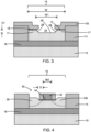
FIGS. 1-4 are cross-sectional views of a semiconductor structure at successive fabrication stages of a processing method in accordance with embodiments of the invention. -
FIG. 5 is a cross-sectional view of a semiconductor structure in accordance with alternative embodiments of the invention. -
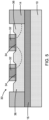
FIGS. 6-7 are cross-sectional views of a semiconductor structure at successive fabrication stages of a processing method in accordance with alternative embodiments of the invention. - With reference to
FIG. 1 and in accordance with embodiments of the invention, asemiconductor substrate 10 is provided that contains a semiconductor material, such as single-crystal silicon. A shallowtrench isolation region 14 may be formed by a shallow trench isolation technique that patterns trenches in thesemiconductor substrate 10 with lithography and etching processes, deposits a dielectric material to overfill the trenches, and planarizes the dielectric material using chemical mechanical polishing and/or an etch back to remove excess dielectric material over atop surface 12 of thesemiconductor substrate 10. The dielectric material contained in the shallowtrench isolation region 14 may be comprised of an electrical insulator, such as silicon dioxide, deposited by chemical vapor deposition. The shallowtrench isolation region 14 surrounds anactive device region 15 of thesemiconductor substrate 10 in which a device structure may be subsequently fabricated. - A high-
resistivity layer 16 is positioned in thesemiconductor substrate 10 beneath theactive device region 15. The electrical resistivity of the high-resistivity layer 16 is significantly greater than the electrical resistivity of thesemiconductor substrate 10 in theactive device region 15 or the bulk portion of thesemiconductor substrate 10 that surrounds theactive device region 15. For example, the high-resistivity layer 16 may be comprised of a polycrystalline semiconductor material, such as polysilicon, formed in thesemiconductor substrate 10 by an amorphizing ion implantation and a subsequent anneal that recrystallizes the amorphous semiconductor material of thesemiconductor substrate 10. The high-resistivity layer 16 may abut the shallowtrench isolation region 14 and, in particular, the high-resistivity layer 16 may abut a lowermost portion of the shallowtrench isolation region 14 such that theactive device region 15 is fully isolated from the bulk portion of thesemiconductor substrate 10, which may improve device performance for a device structure subsequently fabricated in theactive device region 15. -
Dielectric layers opening 21 that extends to a portion of thetop surface 12 of thesemiconductor substrate 10 in theactive device region 15. Thedielectric layer 18 may be comprised of a dielectric material, such as silicon dioxide, grown by thermal oxidation. Thedielectric layer 20 may be comprised of a dielectric material, such as silicon nitride, deposited by chemical vapor deposition. In an embodiment, the opening 21 in thedielectric layers top surface 12 of thesemiconductor substrate 10 in theactive device region 15. - With reference to
FIG. 2 in which like reference numerals refer to like features inFIG. 1 and at a subsequent fabrication stage, adielectric layer 22 is formed at the location of theopening 21 in thedielectric layers dielectric layer 22 may be comprised of a dielectric material, such as silicon dioxide. In an embodiment, thedielectric layer 22 may be comprised of silicon dioxide formed by subjecting the portion of thesemiconductor substrate 10 at the location of the opening 21 to thermal oxidation in an oxidizing atmosphere (e.g., an atmosphere with an oxygen content) using a local oxidation of silicon (LOCOS) process. The oxidizing species (e.g., oxygen) is barred from diffusing through the thickness of thedielectric layer 20 during thermal oxidation, and theopening 21 in thedielectric layer 20 exposes an unprotected portion of thesemiconductor substrate 10 that is thermally oxidized to grow thedielectric layer 22. The oxidizing species laterally diffuses in thesemiconductor substrate 10 beneath thedielectric layer 20 at the side edges of theopening 21 and oxidizes the semiconductor material under the side edges. Because of the gradient inherent in the lateral diffusion of the oxidizing species, thedielectric layer 22 tapers from a full thickness interior of the side edges of theopening 21 to a near-zero thickness beneath thedielectric layer 20, and thedielectric layer 22 is faceted adjacent to the side edges of theopening 21 in thedielectric layer 20. Although not shown, the formation of thedielectric layer 22 may cause thedielectric layer 20 proximate to the side edges of theopening 21 to be deflected upwardly. - With reference to
FIG. 3 in which like reference numerals refer to like features inFIG. 2 and at a subsequent fabrication stage, thedielectric layers dielectric layer 22 are removed by one or more etching processes. The removal of thedielectric layer 22 generates a facetedrecess 24 in thetop surface 12 of thesemiconductor substrate 10. The shape and dimensions of the facetedrecess 24 are defined by the shape and dimensions of the removeddielectric layer 22. The shallowtrench isolation region 14 is positioned to surround the portion of theactive device region 15 including the facetedrecess 24. - The
semiconductor substrate 10 includes asurface 26 inside the facetedrecess 24 that is recessed relative to thetop surface 12 andinclined surfaces 28 that join thesurface 26 to thetop surface 12 at the opposite side edges of the facetedrecess 24. Theinclined surfaces 28 are oriented at an angle relative to thetop surface 12 and at an angle relative to thesurface 26 due to the faceted shape of the removeddielectric layer 22. The facetedrecess 24 penetrates partially through thesemiconductor substrate 10 in theactive device region 15 such that thesurface 26 is located at a depth D1 that may be equal to the distance in a vertical direction between thetop surface 12 and thesurface 26 inside the facetedrecess 24. - The faceted
recess 24 has a width W1 that is less than the full width W of theactive device region 15. As a result, thesemiconductor substrate 10 in theactive device region 15 includes raisedportions 17 that are not recessed, and the facetedrecess 24 is laterally positioned between the raisedportions 17. The raisedportions 17 of thesemiconductor substrate 10 are effectively raised in elevation relative to thesurface 26 inside the facetedrecess 24, and the raisedportions 17 are laterally positioned between the facetedrecess 24 and the shallowtrench isolation region 14. - With reference to
FIG. 4 in which like reference numerals refer to like features inFIG. 3 and at a subsequent fabrication stage, a field-effect transistor 30 may be fabricated by front-end-of-line (FEOL) processing as a device structure in theactive device region 15 of thesemiconductor substrate 10. The field-effect transistor 30 may include agate electrode 32 and a gatedielectric layer 34 formed on thesurface 26 by depositing a layer stack and patterning the layer stack with photolithography and etching processes. Thegate electrode 32 may be comprised of a conductor, such as doped polycrystalline silicon (i.e., polysilicon) or a work function metal, and the gatedielectric layer 34 may be comprised of an electrical insulator, such as silicon dioxide or hafnium oxide. The field-effect transistor 30 may include other elements such as halo regions, lightly doped drain extensions, source/drain regions 36, and sidewall spacers on thegate electrode 32. - The source/
drain regions 36 may be formed by, for example, ion implantation in the raised portions 17 (FIG. 3 ) of thesemiconductor substrate 10. The source/drain regions 36 may be doped (e.g., heavily doped) with a concentration of a dopant, such as an n-type dopant (e.g., arsenic or phosphorus) that provides n-type conductivity. Alternatively, source/drain regions 36 may be doped (e.g., heavily doped) with a concentration of a p-type dopant (e.g., boron) that provides p-type conductivity. As used herein, the term "source/drain region" means a doped region of semiconductor material that can function as either a source or a drain of a field-effect transistor. - The
gate electrode 32 and the gatedielectric layer 34 are positioned on thesurface 26 inside the facetedrecess 24. Thegate electrode 32 is laterally offset in an inward direction from each of theinclined surfaces 28 bordering the facetedrecess 24. In that regard, thegate electrode 32 has a width W2 that is less than the width W1 of the facetedrecess 24 and, in particular, thegate electrode 32 has a width W2 that is less than the contribution of the width of thesurface 26 to the width W1 of the facetedrecess 24. In an embodiment, thegate electrode 32 may be centered between the raisedportions 17 andinclined surfaces 28. In an embodiment, thegate dielectric layer 34 may be positioned on the entirety of thesurface 26, including the portion of thesurface 26 on which thegate electrode 32 is disposed. - Performance metrics characterizing the field-
effect transistor 30 may be improved due to the introduction of thefaceted recess 24. For example, arranging thegate electrode 32 of the field-effect transistor 30 inside thefaceted recess 24 may operate to reduce the off-capacitance of the field-effect transistor 30. - With reference to
FIG. 5 and in accordance with alternative embodiments of the invention, the field-effect transistor 30 may includemultiple gate electrodes 32 to provide a switch field-effect transistor, which may be deployed in a radio-frequency front-end integrated circuit. Thegate electrodes 32 are arranged as multiple parallel gate fingers each positioned inside its ownfaceted recess 24, and thegate electrodes 32 may be joined together at one end to provide a common connection for biasing. - With reference to
FIG. 6 and in accordance with alternative embodiments of the invention, afaceted recess 25 may be formed in thesurface 26 and within thefaceted recess 24. Thefaceted recess 25 may be formed in the same manner as thefaceted recess 24. Thefaceted recess 25 penetrates to asurface 27 of thesemiconductor substrate 10 located at a depth D2 relative to thetop surface 12 that is greater than the depth D1. Thefaceted recess 25 is laterally offset relative to thefaceted recess 24, and thefaceted recess 25 has a width W3 that is less than the width W1 of thefaceted recess 24. The faceted recesses 24, 25 define a dual-depth composite recess that is recessed relative to thetop surface 12 of thesemiconductor substrate 10. - With reference to
FIG. 7 in which like reference numerals refer to like features inFIG. 6 and at a subsequent fabrication stage of the processing method, a multiple-thicknessgate dielectric layer 34 may be formed inside thefaceted recesses gate dielectric layer 34, which may be formed on thesurface 26, has a thickness T1, and another section of thegate dielectric layer 34, which may be formed on thesurface 27, has a thickness T2 that is greater than the thickness T1. In an embodiment, the dual-thicknessgate dielectric layer 34 may be formed by depositing a first dielectric layer with the thickness T1 inside bothfaceted recesses surface 27, and removing non-masked portions of the first dielectric layer with an etching processes, followed by depositing a second dielectric layer with the thickness T2 inside bothfaceted recesses surface 26, and removing non-masked portions of the second dielectric layer with an etching processes. - The field-
effect transistor 30 is subsequently fabricated as a device structure in theactive device region 15 of thesemiconductor substrate 10. Thegate electrode 32 of the field-effect transistor 30, which is positioned on thegate dielectric layer 34 over thesurfaces gate dielectric layer 34. Specifically, the portion of thegate electrode 32 positioned on the section of thegate dielectric layer 34 with thickness T2 is thinner than the portion of thegate electrode 32 positioned on the section of thegate dielectric layer 34 with thickness T1. - The methods as described above are used in the fabrication of integrated circuit chips. The resulting integrated circuit chips can be distributed by the fabricator in raw wafer form (e.g., as a single wafer that has multiple unpackaged chips), as a bare die, or in a packaged form. In the latter case, the chip is mounted in a single chip package (e.g., a plastic carrier, with leads that are affixed to a motherboard or other higher level carrier) or in a multichip package (e.g., a ceramic carrier that has either or both surface interconnections or buried interconnections). In any case, the chip may be integrated with other chips, discrete circuit elements, and/or other signal processing devices as part of either an intermediate product or an end product.
- References herein to terms modified by language of approximation, such as "about", "approximately", and "substantially", are not to be limited to the precise value specified. The language of approximation may correspond to the precision of an instrument used to measure the value and, unless otherwise dependent on the precision of the instrument, may indicate a range of +/- 10% of the stated value(s).
- References herein to terms such as "vertical", "horizontal", etc. are made by way of example, and not by way of limitation, to establish a frame of reference. The term "horizontal" as used herein is defined as a plane parallel to a conventional plane of a semiconductor substrate, regardless of its actual three-dimensional spatial orientation. The terms "vertical" and "normal" refer to a direction perpendicular to the horizontal, as just defined. The term "lateral" refers to a direction within the horizontal plane.
- A feature "connected" or "coupled" to or with another feature may be directly connected or coupled to or with the other feature or, instead, one or more intervening features may be present. A feature may be "directly connected" or "directly coupled" to or with another feature if intervening features are absent. A feature may be "indirectly connected" or "indirectly coupled" to or with another feature if at least one intervening feature is present. A feature "on" or "contacting" another feature may be directly on or in direct contact with the other feature or, instead, one or more intervening features may be present. A feature may be "directly on" or in "direct contact" with another feature if intervening features are absent. A feature may be "indirectly on" or in "indirect contact" with another feature if at least one intervening feature is present. Different features may "overlap" if a feature extends over, and covers a part of, another feature.
- The descriptions of the various embodiments of the present invention have been presented for purposes of illustration but are not intended to be exhaustive or limited to the embodiments disclosed. Many modifications and variations will be apparent to those of ordinary skill in the art without departing from the scope and spirit of the described embodiments. The terminology used herein was chosen to best explain the principles of the embodiments, the practical application or technical improvement over technologies found in the marketplace, or to enable others of ordinary skill in the art to understand the embodiments disclosed herein.
- The invention explicitly discloses the following embodiments:
- A structure comprising:
- a semiconductor substrate including a first surface, a first recess in the first surface, and a second surface inside the first recess;
- a shallow trench isolation region extending from the first surface into the semiconductor substrate, the shallow trench isolation region positioned to surround an active device region including the first recess; and
- a field-effect transistor including a gate electrode positioned on a portion of the second surface.
- The structure of embodiment 1, wherein the field-effect transistor includes a gate dielectric layer on the second surface, and the gate dielectric layer is positioned between the gate electrode and the portion of the second surface.
- The structure of embodiment 2, wherein the gate dielectric layer includes a first section with a first thickness and a second section with a second thickness that is greater than the first thickness.
- The structure of embodiment 3, wherein the gate electrode includes a first portion having a first thickness on the first section of the gate dielectric layer and a second portion having a second thickness on the second section of the gate dielectric layer that is less than the first thickness.
- The structure of embodiment 3 or 4, wherein the semiconductor substrate includes a second recess in the second surface, and the first section of the gate dielectric layer is positioned in the second recess.
- The structure of one of embodiments 1 to 5, further comprising:
a polycrystalline layer in the semiconductor substrate, the polycrystalline layer positioned beneath the active device region and the first recess. - The structure of embodiment 6, wherein the polycrystalline layer abuts the shallow trench isolation region.
- The structure of one of embodiments 1 to 7, wherein the field-effect transistor includes a source/drain region laterally positioned in the semiconductor substrate between the first recess and the shallow trench isolation region.
- The structure of one of embodiments 1 to 8, wherein the semiconductor substrate includes a third surface inside the first recess, the third surface extends at a first angle from the second surface to the first surface of the semiconductor substrate, and the gate electrode is laterally offset from the third surface.
- The structure of embodiment 9, wherein the semiconductor substrate includes a fourth surface inside the first recess, the second surface is positioned between the third surface and the fourth surface, the fourth surface extends at a second angle from the second surface to the first surface of the semiconductor substrate, and the gate electrode is laterally offset from the fourth surface.
- The structure of
embodiment 10, wherein the gate electrode is laterally positioned between the third surface and the fourth surface. - The structure of one of embodiments 1 to 11, wherein the first recess has a first width, and the gate electrode has a second width that is less than the first width.
- The structure of
embodiment 12, wherein the active device region has a third width, and the first width of the first recess is less than the third width. - The structure of one of embodiments 1 to 13, wherein the first recess has a first width, the active device region has a fourth width, and the first width of the first recess is less than the fourth width.
- A method comprising:
- forming a first recess in a first surface of a semiconductor substrate, wherein the semiconductor substrate includes a second surface inside the first recess;
- forming a shallow trench isolation region extending from the first surface into the semiconductor substrate, wherein the shallow trench isolation region is positioned to surround an active device region including the first recess; and
- forming a field-effect transistor including a gate electrode positioned on a portion of the second surface.
- The method of
embodiment 15, wherein the field-effect transistor includes a gate dielectric layer formed between the gate electrode and the portion of the second surface. - The method of
embodiment 16, wherein the gate dielectric layer includes a first section with a first thickness and a second section with a second thickness that is greater than the first thickness. - The method of
embodiment 17, further comprising:
forming a second recess in the second surface, wherein the first section of the gate dielectric layer is positioned in the second recess. - The method of
embodiment - forming a first dielectric layer on the first surface;
- patterning the first dielectric layer to form an opening extending to the first surface;
- oxidizing the semiconductor substrate at a location of the opening to form a second dielectric layer that is faceted; and
- removing the second dielectric layer to form the first recess.
- The method of one of
embodiments 17 to 19, wherein the first recess has a first width, the gate electrode has a second width that is less than the first width, the active device region has a third width, and the first width of the first recess is less than the third width.
Claims (12)
- A structure comprising:a semiconductor substrate including a first surface, a first recess in the first surface, and a second surface inside the first recess;a shallow trench isolation region extending from the first surface into the semiconductor substrate, the shallow trench isolation region positioned to surround an active device region including the first recess; anda field-effect transistor including a gate electrode positioned on a portion of the second surface.
- The structure of claim 1, wherein the field-effect transistor includes a gate dielectric layer on the second surface, and the gate dielectric layer is positioned between the gate electrode and the portion of the second surface.
- The structure of claim 2, wherein the gate dielectric layer includes a first section with a first thickness and a second section with a second thickness that is greater than the first thickness.
- The structure of claim 3, wherein the gate electrode includes a first portion having a first thickness on the first section of the gate dielectric layer and a second portion having a second thickness on the second section of the gate dielectric layer that is less than the first thickness, and/or
wherein the semiconductor substrate includes a second recess in the second surface, and the first section of the gate dielectric layer is positioned in the second recess. - The structure of one of claims 1 to 4, further comprising:
a polycrystalline layer in the semiconductor substrate, the polycrystalline layer positioned beneath the active device region and the first recess, preferably the polycrystalline layer abutting the shallow trench isolation region. - The structure of one of claims 1 to 5, wherein the field-effect transistor includes a source/drain region laterally positioned in the semiconductor substrate between the first recess and the shallow trench isolation region.
- The structure of claim 6, wherein the semiconductor substrate includes a third surface inside the first recess, the third surface extends at a first angle from the second surface to the first surface of the semiconductor substrate, and the gate electrode is laterally offset from the third surface, wherein the semiconductor substrate preferably includes a fourth surface inside the first recess, the second surface is positioned between the third surface and the fourth surface, the fourth surface extends at a second angle from the second surface to the first surface of the semiconductor substrate, and the gate electrode is laterally offset from the fourth surface, the gate electrode being preferably laterally positioned between the third surface and the fourth surface.
- The structure of one of claims 1 to 7, wherein the first recess has a first width and at least one ofthe gate electrode has a second width that is less than the first width, preferably the active device region having a third width and the first width of the first recess being less than the third width, andthe active device region has a fourth width and the first width of the first recess is less than the fourth width.
- A method comprising:forming a first recess in a first surface of a semiconductor substrate, wherein the semiconductor substrate includes a second surface inside the first recess;forming a shallow trench isolation region extending from the first surface into the semiconductor substrate, wherein the shallow trench isolation region is positioned to surround an active device region including the first recess; andforming a field-effect transistor including a gate electrode positioned on a portion of the second surface.
- The method of claim 9, wherein the field-effect transistor includes a gate dielectric layer formed between the gate electrode and the portion of the second surface.
- The method of claim 10, wherein the gate dielectric layer includes a first section with a first thickness and a second section with a second thickness that is greater than the first thickness.
- The method of claim 11, wherein the method further comprises:forming a second recess in the second surface, wherein the first section of the gate dielectric layer is positioned in the second recess, and/orwherein forming the first recess in the first surface of the semiconductor substrate comprises:forming a first dielectric layer on the first surface;patterning the first dielectric layer to form an opening extending to the first surface;oxidizing the semiconductor substrate at a location of the opening to form a second dielectric layer that is faceted; andremoving the second dielectric layer to form the first recess, and/orwherein the first recess has a first width, the gate electrode has a second width that is less than the first width, the active device region has a third width, and the first width of the first recess is less than the third width.
Applications Claiming Priority (1)
| Application Number | Priority Date | Filing Date | Title |
|---|---|---|---|
| US17/708,561 US12230673B2 (en) | 2022-03-30 | 2022-03-30 | Field-effect transistors having a gate electrode positioned inside a substrate recess |
Publications (1)
| Publication Number | Publication Date |
|---|---|
| EP4254505A1 true EP4254505A1 (en) | 2023-10-04 |
Family
ID=83506522
Family Applications (1)
| Application Number | Title | Priority Date | Filing Date |
|---|---|---|---|
| EP22198020.4A Pending EP4254505A1 (en) | 2022-03-30 | 2022-09-27 | Field-effect transistors having a gate electrode positioned inside a substrate recess |
Country Status (2)
| Country | Link |
|---|---|
| US (1) | US12230673B2 (en) |
| EP (1) | EP4254505A1 (en) |
Citations (3)
| Publication number | Priority date | Publication date | Assignee | Title |
|---|---|---|---|---|
| US6528847B2 (en) * | 1998-06-29 | 2003-03-04 | Advanced Micro Devices, Inc. | Metal oxide semiconductor device having contoured channel region and elevated source and drain regions |
| US20150001622A1 (en) * | 2013-06-27 | 2015-01-01 | International Business Machines Corporation | Thin body switch transistor |
| US20210066118A1 (en) * | 2019-08-28 | 2021-03-04 | Globalfoundries Inc. | Semiconductor structures including stacked depleted and high resistivity regions |
Family Cites Families (5)
| Publication number | Priority date | Publication date | Assignee | Title |
|---|---|---|---|---|
| KR100696764B1 (en) * | 2006-03-23 | 2007-03-19 | 주식회사 하이닉스반도체 | Semiconductor element and manufacturing method thereof |
| US7947543B2 (en) | 2008-09-25 | 2011-05-24 | Micron Technology, Inc. | Recessed gate silicon-on-insulator floating body device with self-aligned lateral isolation |
| US9024357B2 (en) | 2011-04-15 | 2015-05-05 | Stmicroelectronics S.R.L. | Method for manufacturing a HEMT transistor and corresponding HEMT transistor |
| US10192779B1 (en) | 2018-03-26 | 2019-01-29 | Globalfoundries Inc. | Bulk substrates with a self-aligned buried polycrystalline layer |
| US11158535B2 (en) | 2019-10-10 | 2021-10-26 | Globalfoundries U.S. Inc. | Multi-depth regions of high resistivity in a semiconductor substrate |
-
2022
- 2022-03-30 US US17/708,561 patent/US12230673B2/en active Active
- 2022-09-27 EP EP22198020.4A patent/EP4254505A1/en active Pending
Patent Citations (3)
| Publication number | Priority date | Publication date | Assignee | Title |
|---|---|---|---|---|
| US6528847B2 (en) * | 1998-06-29 | 2003-03-04 | Advanced Micro Devices, Inc. | Metal oxide semiconductor device having contoured channel region and elevated source and drain regions |
| US20150001622A1 (en) * | 2013-06-27 | 2015-01-01 | International Business Machines Corporation | Thin body switch transistor |
| US20210066118A1 (en) * | 2019-08-28 | 2021-03-04 | Globalfoundries Inc. | Semiconductor structures including stacked depleted and high resistivity regions |
Also Published As
| Publication number | Publication date |
|---|---|
| US12230673B2 (en) | 2025-02-18 |
| US20230317776A1 (en) | 2023-10-05 |
Similar Documents
| Publication | Publication Date | Title |
|---|---|---|
| US11107884B2 (en) | Sealed cavity structures with a planar surface | |
| US8895394B2 (en) | Trench FET with source recess etch | |
| US10580893B2 (en) | Sealed cavity structures with non-planar surface features to induce stress | |
| US10692859B2 (en) | Large area diode co-integrated with vertical field-effect-transistors | |
| US20090001468A1 (en) | Method of fabricating transistor including buried insulating layer and transistor fabricated using the same | |
| US9748239B2 (en) | Fin-double-gated junction field effect transistor | |
| US10559593B1 (en) | Field-effect transistors with a grown silicon-germanium channel | |
| US20190131406A1 (en) | Ldmos finfet structures with shallow trench isolation inside the fin | |
| US20210028306A1 (en) | Manufacturing method of semiconductor device and semiconductor device | |
| EP4421872A1 (en) | Semiconductor structure with device including at least one in-well porous region | |
| US10680065B2 (en) | Field-effect transistors with a grown silicon-germanium channel | |
| CN120390443B (en) | Semiconductor device and manufacturing method thereof | |
| US11843034B2 (en) | Lateral bipolar transistor | |
| US9953831B1 (en) | Device structures with multiple nitrided layers | |
| US12230673B2 (en) | Field-effect transistors having a gate electrode positioned inside a substrate recess | |
| US20240274712A1 (en) | Field-effect transistors with self-aligned p-shield contacts | |
| US10276560B2 (en) | Passive device structure and methods of making thereof | |
| US20230307539A1 (en) | Lateral diffusion field effect transistor with silicon-on-insulator region below field plate | |
| US20040092076A1 (en) | Semiconductor device and fabrication method thereof | |
| US20190131177A1 (en) | Field-effect transistors with fins having independently-dimensioned sections | |
| US12446253B2 (en) | Field effect transistor with adjustable effective gate length | |
| US20240395932A1 (en) | Wraparound gate structure | |
| US20240258421A1 (en) | Field-effect transistors with a high-temperature hardmask and self-aligned p-shield | |
| US12205949B1 (en) | High-voltage semiconductor device structures | |
| US20260068279A1 (en) | Extended drain metal oxide semiconductor device |
Legal Events
| Date | Code | Title | Description |
|---|---|---|---|
| PUAI | Public reference made under article 153(3) epc to a published international application that has entered the european phase |
Free format text: ORIGINAL CODE: 0009012 |
|
| STAA | Information on the status of an ep patent application or granted ep patent |
Free format text: STATUS: REQUEST FOR EXAMINATION WAS MADE |
|
| 17P | Request for examination filed |
Effective date: 20220927 |
|
| AK | Designated contracting states |
Kind code of ref document: A1 Designated state(s): AL AT BE BG CH CY CZ DE DK EE ES FI FR GB GR HR HU IE IS IT LI LT LU LV MC MK MT NL NO PL PT RO RS SE SI SK SM TR |