EP4250880A1 - Method for manufacturing board with roughened surface and method for manufacturing board having plated layer - Google Patents
Method for manufacturing board with roughened surface and method for manufacturing board having plated layer Download PDFInfo
- Publication number
- EP4250880A1 EP4250880A1 EP23155088.0A EP23155088A EP4250880A1 EP 4250880 A1 EP4250880 A1 EP 4250880A1 EP 23155088 A EP23155088 A EP 23155088A EP 4250880 A1 EP4250880 A1 EP 4250880A1
- Authority
- EP
- European Patent Office
- Prior art keywords
- board
- plated layer
- manufacturing
- electrolytic
- plating
- Prior art date
- Legal status (The legal status is an assumption and is not a legal conclusion. Google has not performed a legal analysis and makes no representation as to the accuracy of the status listed.)
- Pending
Links
Images


Classifications
-
- H—ELECTRICITY
- H05—ELECTRIC TECHNIQUES NOT OTHERWISE PROVIDED FOR
- H05K—PRINTED CIRCUITS; CASINGS OR CONSTRUCTIONAL DETAILS OF ELECTRIC APPARATUS; MANUFACTURE OF ASSEMBLAGES OF ELECTRICAL COMPONENTS
- H05K3/00—Apparatus or processes for manufacturing printed circuits
- H05K3/0011—Working of insulating substrates or insulating layers
- H05K3/0017—Etching of the substrate by chemical or physical means
- H05K3/0026—Etching of the substrate by chemical or physical means by laser ablation
-
- H—ELECTRICITY
- H05—ELECTRIC TECHNIQUES NOT OTHERWISE PROVIDED FOR
- H05K—PRINTED CIRCUITS; CASINGS OR CONSTRUCTIONAL DETAILS OF ELECTRIC APPARATUS; MANUFACTURE OF ASSEMBLAGES OF ELECTRICAL COMPONENTS
- H05K3/00—Apparatus or processes for manufacturing printed circuits
- H05K3/38—Improvement of the adhesion between the insulating substrate and the metal
- H05K3/386—Improvement of the adhesion between the insulating substrate and the metal by the use of an organic polymeric bonding layer, e.g. adhesive
- H05K3/387—Improvement of the adhesion between the insulating substrate and the metal by the use of an organic polymeric bonding layer, e.g. adhesive for electroless plating
-
- B—PERFORMING OPERATIONS; TRANSPORTING
- B23—MACHINE TOOLS; METAL-WORKING NOT OTHERWISE PROVIDED FOR
- B23K—SOLDERING OR UNSOLDERING; WELDING; CLADDING OR PLATING BY SOLDERING OR WELDING; CUTTING BY APPLYING HEAT LOCALLY, e.g. FLAME CUTTING; WORKING BY LASER BEAM
- B23K26/00—Working by laser beam, e.g. welding, cutting or boring
- B23K26/0006—Working by laser beam, e.g. welding, cutting or boring taking account of the properties of the material involved
-
- B—PERFORMING OPERATIONS; TRANSPORTING
- B23—MACHINE TOOLS; METAL-WORKING NOT OTHERWISE PROVIDED FOR
- B23K—SOLDERING OR UNSOLDERING; WELDING; CLADDING OR PLATING BY SOLDERING OR WELDING; CUTTING BY APPLYING HEAT LOCALLY, e.g. FLAME CUTTING; WORKING BY LASER BEAM
- B23K26/00—Working by laser beam, e.g. welding, cutting or boring
- B23K26/02—Positioning or observing the workpiece, e.g. with respect to the point of impact; Aligning, aiming or focusing the laser beam
- B23K26/06—Shaping the laser beam, e.g. by masks or multi-focusing
- B23K26/062—Shaping the laser beam, e.g. by masks or multi-focusing by direct control of the laser beam
- B23K26/0622—Shaping the laser beam, e.g. by masks or multi-focusing by direct control of the laser beam by shaping pulses
- B23K26/0624—Shaping the laser beam, e.g. by masks or multi-focusing by direct control of the laser beam by shaping pulses using ultrashort pulses, i.e. pulses of 1 ns or less
-
- B—PERFORMING OPERATIONS; TRANSPORTING
- B23—MACHINE TOOLS; METAL-WORKING NOT OTHERWISE PROVIDED FOR
- B23K—SOLDERING OR UNSOLDERING; WELDING; CLADDING OR PLATING BY SOLDERING OR WELDING; CUTTING BY APPLYING HEAT LOCALLY, e.g. FLAME CUTTING; WORKING BY LASER BEAM
- B23K26/00—Working by laser beam, e.g. welding, cutting or boring
- B23K26/352—Working by laser beam, e.g. welding, cutting or boring for surface treatment
- B23K26/3568—Modifying rugosity
- B23K26/3584—Increasing rugosity, i.e. roughening
-
- H—ELECTRICITY
- H05—ELECTRIC TECHNIQUES NOT OTHERWISE PROVIDED FOR
- H05K—PRINTED CIRCUITS; CASINGS OR CONSTRUCTIONAL DETAILS OF ELECTRIC APPARATUS; MANUFACTURE OF ASSEMBLAGES OF ELECTRICAL COMPONENTS
- H05K3/00—Apparatus or processes for manufacturing printed circuits
- H05K3/10—Apparatus or processes for manufacturing printed circuits in which conductive material is applied to the insulating support in such a manner as to form the desired conductive pattern
- H05K3/14—Apparatus or processes for manufacturing printed circuits in which conductive material is applied to the insulating support in such a manner as to form the desired conductive pattern using spraying techniques to apply the conductive material, e.g. vapour evaporation
- H05K3/16—Apparatus or processes for manufacturing printed circuits in which conductive material is applied to the insulating support in such a manner as to form the desired conductive pattern using spraying techniques to apply the conductive material, e.g. vapour evaporation by cathodic sputtering
-
- H—ELECTRICITY
- H05—ELECTRIC TECHNIQUES NOT OTHERWISE PROVIDED FOR
- H05K—PRINTED CIRCUITS; CASINGS OR CONSTRUCTIONAL DETAILS OF ELECTRIC APPARATUS; MANUFACTURE OF ASSEMBLAGES OF ELECTRICAL COMPONENTS
- H05K3/00—Apparatus or processes for manufacturing printed circuits
- H05K3/10—Apparatus or processes for manufacturing printed circuits in which conductive material is applied to the insulating support in such a manner as to form the desired conductive pattern
- H05K3/18—Apparatus or processes for manufacturing printed circuits in which conductive material is applied to the insulating support in such a manner as to form the desired conductive pattern using precipitation techniques to apply the conductive material
-
- H—ELECTRICITY
- H05—ELECTRIC TECHNIQUES NOT OTHERWISE PROVIDED FOR
- H05K—PRINTED CIRCUITS; CASINGS OR CONSTRUCTIONAL DETAILS OF ELECTRIC APPARATUS; MANUFACTURE OF ASSEMBLAGES OF ELECTRICAL COMPONENTS
- H05K3/00—Apparatus or processes for manufacturing printed circuits
- H05K3/38—Improvement of the adhesion between the insulating substrate and the metal
- H05K3/381—Improvement of the adhesion between the insulating substrate and the metal by special treatment of the substrate
-
- H—ELECTRICITY
- H05—ELECTRIC TECHNIQUES NOT OTHERWISE PROVIDED FOR
- H05K—PRINTED CIRCUITS; CASINGS OR CONSTRUCTIONAL DETAILS OF ELECTRIC APPARATUS; MANUFACTURE OF ASSEMBLAGES OF ELECTRICAL COMPONENTS
- H05K2203/00—Indexing scheme relating to apparatus or processes for manufacturing printed circuits covered by H05K3/00
- H05K2203/07—Treatments involving liquids, e.g. plating, rinsing
- H05K2203/0756—Uses of liquids, e.g. rinsing, coating, dissolving
- H05K2203/0759—Forming a polymer layer by liquid coating, e.g. a non-metallic protective coating or an organic bonding layer
-
- H—ELECTRICITY
- H05—ELECTRIC TECHNIQUES NOT OTHERWISE PROVIDED FOR
- H05K—PRINTED CIRCUITS; CASINGS OR CONSTRUCTIONAL DETAILS OF ELECTRIC APPARATUS; MANUFACTURE OF ASSEMBLAGES OF ELECTRICAL COMPONENTS
- H05K2203/00—Indexing scheme relating to apparatus or processes for manufacturing printed circuits covered by H05K3/00
- H05K2203/09—Treatments involving charged particles
- H05K2203/095—Plasma, e.g. for treating a substrate to improve adhesion with a conductor or for cleaning holes
-
- H—ELECTRICITY
- H05—ELECTRIC TECHNIQUES NOT OTHERWISE PROVIDED FOR
- H05K—PRINTED CIRCUITS; CASINGS OR CONSTRUCTIONAL DETAILS OF ELECTRIC APPARATUS; MANUFACTURE OF ASSEMBLAGES OF ELECTRICAL COMPONENTS
- H05K2203/00—Indexing scheme relating to apparatus or processes for manufacturing printed circuits covered by H05K3/00
- H05K2203/10—Using electric, magnetic and electromagnetic fields; Using laser light
- H05K2203/107—Using laser light
-
- H—ELECTRICITY
- H05—ELECTRIC TECHNIQUES NOT OTHERWISE PROVIDED FOR
- H05K—PRINTED CIRCUITS; CASINGS OR CONSTRUCTIONAL DETAILS OF ELECTRIC APPARATUS; MANUFACTURE OF ASSEMBLAGES OF ELECTRICAL COMPONENTS
- H05K2203/00—Indexing scheme relating to apparatus or processes for manufacturing printed circuits covered by H05K3/00
- H05K2203/11—Treatments characterised by their effect, e.g. heating, cooling, roughening
-
- H—ELECTRICITY
- H05—ELECTRIC TECHNIQUES NOT OTHERWISE PROVIDED FOR
- H05K—PRINTED CIRCUITS; CASINGS OR CONSTRUCTIONAL DETAILS OF ELECTRIC APPARATUS; MANUFACTURE OF ASSEMBLAGES OF ELECTRICAL COMPONENTS
- H05K3/00—Apparatus or processes for manufacturing printed circuits
- H05K3/0011—Working of insulating substrates or insulating layers
- H05K3/0017—Etching of the substrate by chemical or physical means
- H05K3/0026—Etching of the substrate by chemical or physical means by laser ablation
- H05K3/0032—Etching of the substrate by chemical or physical means by laser ablation of organic insulating material
-
- H—ELECTRICITY
- H05—ELECTRIC TECHNIQUES NOT OTHERWISE PROVIDED FOR
- H05K—PRINTED CIRCUITS; CASINGS OR CONSTRUCTIONAL DETAILS OF ELECTRIC APPARATUS; MANUFACTURE OF ASSEMBLAGES OF ELECTRICAL COMPONENTS
- H05K3/00—Apparatus or processes for manufacturing printed circuits
- H05K3/10—Apparatus or processes for manufacturing printed circuits in which conductive material is applied to the insulating support in such a manner as to form the desired conductive pattern
- H05K3/18—Apparatus or processes for manufacturing printed circuits in which conductive material is applied to the insulating support in such a manner as to form the desired conductive pattern using precipitation techniques to apply the conductive material
- H05K3/181—Apparatus or processes for manufacturing printed circuits in which conductive material is applied to the insulating support in such a manner as to form the desired conductive pattern using precipitation techniques to apply the conductive material by electroless plating
Definitions
- the present disclosure relates to a method for manufacturing a board with a roughened surface and a method for manufacturing a board having a plated layer.
- a large capacity and simultaneous connection are required for a mobile communication system, and in order to fulfill these performances, a high-density micro wiring board is desired.
- Patent Literature 1 JP 2021-55174 A discloses a method for modifying a surface of a resin molding and forming a metal film.
- the method includes a first step of irradiating a resin molding surface layer with a laser beam with a wavelength of 194 nm to 1064 nm at a low output to vaporize a vulnerable layer on the molding surface and moisture contained in the vulnerable layer by light energy, which inhibit adhesive bonding between the resin molding and an electroless plating film, a second step of causing a molecular bonding agent to adhere to the molding surface layer by applying the molecular bonding agent for the adhesive bonding of a plating film to be formed at a later step to the laser-irradiated resin molding, and subsequently exposing it to UV light having a wavelength of 185 nm to 365 nm, a third step of supporting a metal catalyst that becomes an electroless plating catalyst on the molecular bonding agent that adheres to the molding surface layer, and a fourth step of
- Patent Literature 1 JP 2021-55174 A
- Patent Literature 1 JP 2021-55174 A
- JP 2021-55174 A specifies vaporizing low molecular weight components and moisture that remain in the resin molding surface layer, applying the molecular bonding agent to the resin molding surface layer and providing the electroless plated layer after the molecular bonding agent adheres, and the like. If a board having a plated layer is manufactured by the invention disclosed in JP 2021-55174 A , an extremely complicated process would be required.
- the present disclosure provides a method for manufacturing a board with a roughened surface and a method for manufacturing a board having a plated layer that allow easily manufacturing the board having a plated layer.
- the inventors have intensively studied to solve the above-described problem and found that a board having a plated layer can be easily manufactured from a board acquired by performing laser ablation under specific conditions. Thus, the present disclosure has been completed.
- the disclosure provides the method for manufacturing a board with a roughened surface and the method for manufacturing a board having a plated layer, which facilitate the manufacturing of the board having a plated layer.
- the present disclosure can provide the board with a roughened surface.
- the following describes in detail a method for manufacturing a board with a roughened surface, a board with a roughened surface, and a method for manufacturing a board having a plated layer of the embodiment.
- the method for manufacturing a board with a roughened surface of the embodiment is a method for manufacturing a board with a surface roughened for wiring formation and a method for manufacturing a board that includes a step of performing laser ablation on a board containing a resin at least on a surface and in which a laser light irradiated in the laser ablation is a laser light having a pulse width of 1 ps or less, a wavelength of 320 nm or more, and an output of 1 W or less.
- the method for manufacturing a board with a roughened surface of the embodiment performing the laser ablation under specific conditions allows forming a large number of fine unevenness on the surface of the acquired board.
- the board acquired by the embodiment (the board with a roughened surface) has a large number of fine unevenness and a large functional group amount. Therefore, a plated layer formed on the acquired board has an excellent adhesive strength between the plated layer and the board.
- the board containing a resin at least on a surface on which the laser ablation is to be performed is not specifically limited, including conventional boards for wiring formation.
- the resin include polytetrafluoroethylene (PTFE), liquid crystal polymer (LCP), polyphenylene ether (PPE), modified polyphenylene ether (m-PPE), polyimide (PI), modified polyimide (MPI), bismaleimide triazine resin (BT), epoxy resin, and Low-k epoxy resin (low-dielectric constant (Low-Dk) and low-dielectric loss tangent (Low-Df) epoxy resin).
- PTFE polytetrafluoroethylene
- LCP liquid crystal polymer
- PPE polyphenylene ether
- m-PPE modified polyphenylene ether
- PI polyimide
- MPI modified polyimide
- BT bismaleimide triazine resin
- epoxy resin and Low-k epoxy resin (low-dielectric constant (Low-Dk) and low-di
- the resin may be a high frequency-compatible low-dielectric board applicable to high-speed communications (for example, fifth-generation mobile communication systems and sixth-generation mobile communication systems) and millimeter-wave compatible communications (for example, automotive applications).
- the laser ablation is performed on a board.
- the laser ablation is performed by irradiating a surface of the board with a specific laser light, and more specifically, by irradiating the surface of the board on which the resin exists with a laser light.
- the surface of the board only needs to contain a resin and may further contain components other than the resin.
- the components other than the resin include glass fiber, a silica-based filler, a ceramic-based filler, Al 2 O 3 , AlN, and BN.
- the board may be a board having a structure with one layer that is formed only from a layer formed from the resin or may be a board having a structure with two or more layers (multi-layer structure) that has a layer formed from the resin and another layer.
- the other layer is not specifically limited.
- the laser light irradiated in the laser ablation is a laser light having a pulse width of 1 ps or less, a wavelength of 320 nm or more, and an output of 1 W or less.
- the laser light may be a laser light having a pulse width of 0.1 ps or more in one aspect.
- the pulse width may be 0.9 ps or less, or may be 0.85 ps or less in some embodiments.
- the pulse width may be 0.2 ps or more, or may be 0.3 ps or more in some embodiments.
- the laser light may be a laser light having a wavelength of 1064 nm or less in one aspect.
- the wavelength of a laser light differs depending on a light source (laser medium). and for example, using Yb:YAG allows emitting a laser light having a wavelength of 1030 nm and a laser light having a wavelength of 515 nm (second harmonic) , and using YAG allows emitting a laser light having a wavelength of 1064 nm, a laser light having a wavelength of 532 nm (second harmonic), and a laser light having a wavelength of 355 nm (third harmonic).
- the light source for example, Yb:YAG, YAG, or the like can be used.
- the laser light is a laser light having an output of 0.05 W or more in one aspect.
- the output may be 0.8 W or less, or may be 0.6 W or less in some embodiments.
- the output may be 0.07 W or more, or may be 0.1 W or more in some embodiments.
- Energy fluence in performing the laser ablation may be 15 ⁇ J/cm 2 or less, may be 13 ⁇ J/cm 2 or less, or may be 10 ⁇ J/cm 2 or less in some embodiments.
- the energy fluence may be 1 ⁇ J/cm 2 or more, or may be 5 ⁇ J/cm 2 or more in some embodiments.
- An apparatus used in the laser ablation only needs to be capable of emitting the laser light, and is not especially limited.
- Examples of the apparatus include LodeStone (manufactured by Esi) and Monaco series (COHERENT, Inc.).
- the board with a roughened surface of the embodiment is a board that contains a resin at least on a surface and has an arithmetic mean height Sa of 50 to 200 nm and a functional group amount (area ratio) in a C1s spectrum obtained from an XPS (X-ray photoelectron spectroscopy) spectrum of 10% or more.
- the board is usually used as a board for wiring formation.
- the board with a roughened surface of the embodiment can be manufactured by the method for manufacturing a board with a roughened surface described above.
- the board has fine unevenness, that is, the surface is roughened.
- a plated layer formed on the board with a roughened surface of the embodiment may have an excellent adhesive strength between the plated layer and the board.
- the arithmetic mean height Sa of the board with a roughened surface can be measured using a laser roughness meter.
- the functional group amount (area ratio) is 10% or more, may be 11% or more, or may be 12% or more in some embodiments.
- the functional group amount (area ratio) is usually 20% or less, may be 17% or less, or may be 15% or less in some embodiments.
- the present disclosure has three broadly divided embodiments. Since the board having a plated layer acquired by the method for manufacturing a board having a plated layer has an excellent peel strength of the plated layer, the board can be used for various applications, such as high-density micro wiring boards, which are required in high-speed communications (such as fifth-generation mobile communication systems and sixth-generation mobile communication systems) and millimeter-wave compatible communications (such as automotive applications).
- high-density micro wiring boards which are required in high-speed communications (such as fifth-generation mobile communication systems and sixth-generation mobile communication systems) and millimeter-wave compatible communications (such as automotive applications).
- Examples of a metal constituting the plated layer include copper, gold, argentum, nickel, chrome, and aluminum.
- the metal may be copper or gold, and may be copper in some embodiments.
- the method for manufacturing a board having a plated layer of Embodiment-A is a method for manufacturing a board having a plated layer.
- the method includes a step of forming an electroless plated layer by performing electroless plating on the surface of a board acquired by the method for manufacturing a board of the above embodiment or the board of the above embodiment, a step of forming an electrolytic plated layer by performing electrolytic plating on the electroless plated layer, and a step of performing an annealing treatment on the board on which the electrolytic plated layer is formed.
- the method for manufacturing a board having a plated layer of Embodiment-B is a method for manufacturing a board having a plated layer.
- the method includes a step of forming a dry plated layer by performing dry plating on the surface of a board acquired by the method for manufacturing a board of the above embodiment or the board of the above embodiment, a step of forming an electrolytic plated layer by performing electrolytic plating on the dry plated layer, and a step of performing an annealing treatment on the board on which the electrolytic plated layer is formed.
- the method for manufacturing a board having a plated layer of Embodiment-C is a method for manufacturing a board having a plated layer.
- the method includes a step of forming a plated layer by performing plating on the surface of a board acquired by the method for manufacturing a board of the above embodiment or the board of the above embodiment, and a step of performing a laser annealing treatment on the formed plated layer.
- the method for manufacturing a board having a plated layer of Embodiment-A includes a step of forming an electroless plated layer by performing electroless plating on the surface of a board acquired by the method for manufacturing a board of the above embodiment or the board of the above embodiment.
- An electroless plating solution can be selected according to a metal type constituting the plated layer, and any electroless plating solution including a publicly known autocatalytic electroless plating solution and the like can be used without specific limitations.
- an electroless plating solution an electroless copper plating solution, an electroless gold plating solution, an electroless silver plating solution, an electroless nickel plating solution, an electroless chrome plating solution, or the like can be used.
- the electroless copper plating solution is usually used.
- the plating conditions of the electroless plating publicly known conditions can be appropriately used.
- the electroless plated layer may have an average thickness of 600 nm or less, may have an average thickness of 240 nm to 160 nm, or may have an average thickness of 220 nm to 180 nm in some embodiments.
- the electroless plated layer may be an electroless copper plated layer in one aspect.
- a board having a plated layer may be acquired by the method for manufacturing a board having a plated layer of Embodiment-A especially because the board is strongly coupled to the plated layer and has a high peel strength.
- a board having a plated layer may be acquired by the methods for manufacturing a board having a plated layer of Embodiment-A, Embodiment-B, and Embodiment-C because the board has an excellent adhesive strength between the plated layer and the board without providing an adhesive layer formed from Cr or Ti that was provided in performing the conventional dry plating.
- the method for manufacturing a board having a plated layer of Embodiment-B includes a step of forming a dry plated layer by performing dry plating on the surface of a board acquired by the method for manufacturing a board of the above embodiment or the board of the above embodiment.
- the dry plating includes a sputtering method, an ion plating method, and a vacuum vapor deposition method.
- the dry plating may be the sputtering method from the aspect of the adhesion with a board. That is, the dry plated layer may be a sputtered layer in one aspect.
- copper, gold, argentum, nickel, chrome, aluminum, or the like can be used, and copper is usually used for the application of wiring boards.
- the dry plating can be performed by appropriately applying publicly known conditions. That is, the dry plating can be performed by the publicly known sputtering method, ion plating method, vacuum vapor deposition method, or the like.
- the dry plated layer may have an average thickness of 600 nm or less, may have an average thickness of 250 nm to 150 nm, or may have an average thickness of 240 nm to 160 nm in some embodiments.
- the dry plated layer may be a dry copper plated layer in one aspect.
- the board having a plated layer acquired by the method for manufacturing a board having a plated layer of Embodiment-B has a sufficiently high peel strength even though the plated layer adjacent to the board is a dry plated layer formed by the dry plating by which it is generally difficult to couple to a board.
- the dry plating may be performed because the dry plating tends to have less environmental load compared with the electroless plating that is a kind of wet plating.
- the method for manufacturing a board having a plated layer of Embodiment-B may include, before the step of forming a dry plated layer, a step of performing a plasma treatment on the surface of a board acquired by the method for manufacturing a board of the above embodiment or the board of the above embodiment in one aspect.
- the step of performing a plasma treatment may be provided because the functional group amount (area ratio) in the C1s spectrum obtained from the XPS spectrum of the board can be further improved.
- the step of performing a plasma treatment may be performed before the step of forming an electroless plated layer in another method, for example, in the method for manufacturing a board having a plated layer of Embodiment-A.
- the plasma treatment may be at least one kind of plasma treatment selected from an H 2 /Ar plasma treatment and an O 2 /Ar plasma treatment.
- the H 2 /Ar plasma treatment is a method of performing a plasma treatment on a board using hydrogen and argon
- the O 2 /Ar plasma treatment is a method of performing a plasma treatment on a board using oxygen and argon
- the H 2 /Ar plasma treatment and the O 2 /Ar plasma treatment can be each performed by appropriately applying publicly known conditions.
- the plasma treatment the H 2 /Ar plasma treatment and the O 2 /Ar plasma treatment may be performed, and the O 2 /Ar plasma treatment may be performed after performing the H 2 /Ar plasma treatment in some embodiments.
- Performing the H 2 /Ar plasma treatment can provide a clean surface, and subsequently performing the O 2 /Ar plasma treatment can introduce the functional group.
- the method for manufacturing a board having a plated layer of Embodiment-A includes a step of forming an electrolytic plated layer by performing electrolytic plating on the electroless plated layer.
- the method for manufacturing a board having a plated layer of Embodiment-B includes a step of forming an electrolytic plated layer by performing electrolytic plating on the dry plated layer. These steps differ in whether an object on which electrolytic plating is performed is an electroless plated layer or a dry plated layer, and other than that, these steps can be performed similarly.
- an electrolytic plating solution an electrolytic copper plating solution, an electrolytic gold plating solution, an electrolytic silver plating solution, an electrolytic nickel plating solution, an electrolytic chrome plating solution, an electrolytic tin plating solution, or the like can be used.
- the electrolytic copper plating solution is usually used.
- the plating conditions of the electrolytic plating publicly known conditions can be appropriately applied.
- a solid electrolyte deposition (SED) that is a plating method using a solid-state electrolyte membrane may be employed.
- the electrolytic plated layer may have an average line width of wiring (simply referred to also as width) of 30 ⁇ m or less, may have an average line width of 10 ⁇ m or less, or may have an average line width of 5 ⁇ m or less in some embodiments.
- the average line width may be 1 ⁇ m or more.
- the aspect ratio (thickness/width) of the thickness to the width of the wiring may be 0.85 to 1.15, or may be 0.9 to 1.1 in some embodiments.
- the electrolytic plated layer may be an electrolytic copper plated layer in one aspect.
- the electroless plated layer and the electrolytic plated layer, or the dry plated layer and the electrolytic plated layer may be layers formed from the same type of metal, or may be layers formed from copper in some embodiments.
- the method for manufacturing a board having a plated layer of Embodiment-A includes a step of performing an annealing treatment on the board on which the electrolytic plated layer is formed.
- the method for manufacturing a board having a plated layer of Embodiment-B also includes a step of performing an annealing treatment on the board on which the electrolytic plated layer is formed.
- the annealing treatment is generally performed by heating the board on which an electrolytic plated layer is formed. While the heating temperature varies depending on the type of a resin constituting the board, the type of metal constituting the plated layer, and the like, it is, for example, 100°C to 210°C, and may be 110°C to 200°C in some embodiments.
- the annealing treatment is usually performed by heating the board at a temperature, which is the glass transition point (Tg) or more of the resin constituting the board, and for a time period in which its shape retention is secured. In the annealing treatment, the temperature may be increased in phases from a low temperature in one aspect.
- a low-temperature annealing treatment can be performed at 100°C to 140°C, or at 110°C to 140°C in some embodiments, and subsequently, a high-temperature annealing treatment can be performed at 150°C to 210°C, or at 150°C to 200°C in some embodiments.
- the annealing treatment is performed at a constant temperature, for example, the annealing treatment is performed at 150°C to 210°C, or at 160°C to 200°C in some embodiments.
- heating at a temperature of Tg of the resin or more is performed usually for 10 minutes to 90 minutes, or for 30 minutes to 60 minutes in some embodiments.
- each phase is performed usually for 10 minutes to 90 minutes, or for 30 minutes to 60 minutes in some embodiments.
- the annealing treatment may be performed in air, or may be performed in an inert gas, such as nitrogen and noble gas. From the aspect of the cost, the annealing treatment may be performed in air, and from the aspect of suppressing side reactions, it may be performed in an inert gas.
- an inert gas such as nitrogen and noble gas.
- the annealing treatment may be performed under normal pressure, under reduced pressure, or under increased pressure, it is usually performed under normal pressure.
- the annealing treatment is generally performed by heating the board on which an electrolytic plated layer is formed, it may be performed by performing a laser annealing treatment on the electrolytic plated layer of the board on which an electrolytic plated layer is formed.
- the laser annealing treatment is synonymous with the laser annealing treatment in the method for manufacturing a board having a plated layer of Embodiment-C.
- the method for manufacturing a board having a plated layer of Embodiment-C includes a step of forming a plated layer by performing plating on the surface of a board acquired by the method for manufacturing a board of the above embodiment or the board of the above embodiment.
- the plating in the step is not specifically limited, and examples of the plating include electroless plating, dry plating, electrolytic plating, and any combination thereof.
- the step of forming a plated layer may have a step of forming an electroless plated layer by performing electroless plating on the surface of a board acquired by the method for manufacturing a board of the above embodiment or the board of the above embodiment and a step of forming an electrolytic plated layer by performing electrolytic plating on the electroless plated layer, or may include a step of forming a dry plated layer by performing dry plating on the surface of a board acquired by the method for manufacturing a board of the above embodiment or the board of the above embodiment, and a step of forming an electrolytic plated layer by performing electrolytic plating on the dry plated layer. That is, by the methods described in Embodiment-A and Embodiment-B described above, the electroless plated layer and the electrolytic plated layer may be formed, or the dry plated layer and the electrolytic plated layer may be formed.
- the method for manufacturing a board having a plated layer of Embodiment-C includes a step of performing a laser annealing treatment on the formed plated layer.
- the laser annealing treatment is a method for performing an annealing treatment on the portion irradiated with a laser light by irradiating the formed plated layer with the laser light.
- the wavelength of the laser light irradiated on the plated layer may be a wavelength that can be absorbed by the plated layer. While the wavelength of the laser light irradiated on the plated layer varies depending on the metal type of the plated layer, it is usually 600 nm or less, and may be 550 nm or less in some embodiments. While the lower limit of the wavelength is not specifically limited, for example, it may be 200 nm or more in some embodiments.
- Irradiation conditions of the laser light are not specifically limited insofar as the interface temperature between the plated layer and the board is the glass transition point or more of the resin constituting the portion of the board.
- the irradiation conditions can be appropriately set depending on the types of the device and the resin, the metal type, thickness, and the like of the plated layer.
- the laser annealing treatment varies depending on the area and the like of the portion to be annealed, it is desirable that the laser annealing treatment exhibits a sufficient peel strength generally in a brief time, for example, within 10 minutes, or within 3 minutes of treatment in some embodiments, compared with the annealing treatment by heating. Since the laser annealing treatment allows local heating of interface between the board and the plated layer by a laser light, heating can be performed without concerns about shape retention of the board. In view of this, heating may be performed by a laser light to a temperature exceeding the temperature (for example, 200°C, although it varies depending on the type of the resin) at which the shape retention can be secured in a case of general heating, that is, in a case of heating the entire board.
- the temperature for example, 200°C, although it varies depending on the type of the resin
- ABF films (ABF GX92, manufactured by Ajinomoto Fine-Techno Co., Inc.) were used.
- ABF GX92 is distributed in a state where a layer formed from an insulating material (epoxy resin containing a silica-based filler) is disposed on a PET film.
- ABF GX92 in which the PET film was peeled off and the layer formed from the insulating material (epoxy resin containing a silica-based filler) was attached on a supporting member (epoxy resin containing glass fiber) was used as the ABF film (board).
- the surface on the supporting member side but the surface on the side of the layer formed from the insulating material (hereinafter simply referred to as the surface) was a target on which laser ablation or wet roughening was performed.
- Laser ablation (target roughness Sa 200 nm) was performed by irradiating the surface of the ABF film with a laser light under the conditions below.
- Wet roughening (target roughness Sa 200 nm) was performed on the surface of the ABF film by a desmear process with permanganic acid.
- the surface roughness Sa (arithmetic mean heights) was obtained with a confocal laser roughness meter.
- the surface roughness Sa of the ABF film acquired in Example 1 on which the laser ablation was performed was 170 nm
- the surface roughness Sa of the ABF film acquired in Comparative Example 1 on which the wet roughening was performed was 220 nm.
- Sa is the arithmetic mean height of a contour curved surface and means the average absolute value of the vertical coordinate values z (x, y) in reference region A.
- the SEM images are illustrated in FIG. 1 .
- the functional group amount increases by performing the processes of Example 1 and Comparative Example 1. Especially in Example 1, compared with the ABF film before the processes and the ABF film acquired in Comparative Example 1 on which the wet roughening was performed, the functional group amount was confirmed to substantially increase.
- the increase of the functional group amount is considered to be a change with which the adhesive strength with the plated layer can expect to improve in some embodiments.
- Electroless copper plating was performed on the surface of the ABF film acquired in Example 1 on which the laser ablation was performed, under the conditions below to form an electroless copper plated layer. Subsequently, electrolytic copper plating was performed on the electroless copper plated layer under the conditions below to form an electrolytic copper plated layer.
- a heat treatment was performed on the board on which the electrolytic copper plated layer was formed, under air atmosphere at 180°C for 30 minutes to acquire a board having a copper plated layer.
- Electroless copper plating was performed on the surface of the ABF film acquired in Comparative Example 1 on which the wet roughening was performed, under the conditions below to form an electroless copper plated layer. Subsequently, electrolytic copper plating was performed on the electroless copper plated layer under the conditions below to form an electrolytic copper plated layer.
- a heat treatment was performed on the board on which the electrolytic copper plated layer was formed, under air atmosphere at 180°C for 30 minutes to acquire a board having a copper plated layer.
- a 10 mm width slit was made in the electrolytic copper plated layers using a cutter, and the peel strength (kN/m) was measured with a peel strength tester (Digital Force Gauge ZTA-DPU, manufactured by IMADA CO., LTD.). The measurement results of the peel strength were shown in FIG. 3 .
- Example 2 the peel strength substantially improves compared with Comparative Example 2.
- Comparative Example 2 it was also possible to achieve a general target peel strength (0.6 kN/m).
- the board having the copper plated layer acquired in Example 2 had further improved peel strength, it was indicated that the board having the copper plated layer acquired in Example 2 is useful for a high-density micro wiring board.
- An H 2 /Ar plasma treatment was performed on the ABF film acquired in Example 1 on which the laser ablation was performed, under the conditions below, and subsequently, an O 2 /Ar plasma treatment was performed.
- a heat treatment (low-temperature annealing treatment) was performed on the board on which the electrolytic copper plated layer was formed, under air atmosphere at 120°C for 30 minutes, and subsequently, a heat treatment (high-temperature annealing treatment) was performed at 200°C for 1 hour to acquire a board having a copper plated layer.
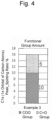
- Example 3 An XPS observation was performed under the conditions below on the surface of the ABF film acquired in Example 3 on which the H 2 /Ar plasma treatment and the O 2 /Ar plasma treatment were performed, a C1s (1s orbital of carbon atoms) spectrum was acquired, and peak splitting was performed to calculate the functional group amount (area ratio).
- the functional group amount is illustrated in FIG. 4 .
- the functional group amount was further increased by performing the H 2 /Ar plasma treatment and the O 2 /Ar plasma treatment.
- the increase of the functional group amount is considered to be a change with which the adhesive strength with the plated layer can expect to improve in some embodiments.
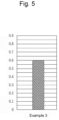
- a 10 mm width slit was made in the electrolytic copper plated layer using a cutter, and the peel strength (kN/m) was measured with the peel strength tester (Digital Force Gauge ZTA-DPU, manufactured by IMADA CO., LTD.). The measurement result of the peel strength is shown in FIG. 5 .
- An electroless copper plated layer and an electrolytic copper plated layer were formed on the surface of the ABF film acquired in Example 1 on which the laser ablation was performed by the method described in Example 2.
- a board having a copper plated layer was acquired by performing a laser annealing treatment on the board on which the electrolytic copper plated layer was formed, under the conditions below.
- the laser annealing treatment was performed by irradiating the electrolytic copper plated layer with a laser light under the conditions below.
- a board having a copper plated layer was acquired similarly to Example 4 except that the laser annealing treatment was not performed.
- the board having a copper plated layer that has improved peel strength and exceeds the general target peel strength (0.6 kN/m) is acquired by performing the laser annealing treatment, compared with a case where the laser annealing treatment is not performed. It was indicated that the laser annealing treatment allows acquiring the board having a copper plated layer with excellent peel strength in a shorter time than a general treatment by heat.
- Upper limit values and/or lower limit values of respective numerical ranges described in this description can be appropriately combined to specify an intended range.
- upper limit values and lower limit values of the numerical ranges can be appropriately combined to specify an intended range
- upper limit values of the numerical ranges can be appropriately combined to specify an intended range
- lower limit values of the numerical ranges can be appropriately combined to specify an intended range.
Landscapes
- Engineering & Computer Science (AREA)
- Manufacturing & Machinery (AREA)
- Microelectronics & Electronic Packaging (AREA)
- Physics & Mathematics (AREA)
- Optics & Photonics (AREA)
- Plasma & Fusion (AREA)
- Mechanical Engineering (AREA)
- Manufacturing Of Printed Wiring (AREA)
- Other Surface Treatments For Metallic Materials (AREA)
- Chemically Coating (AREA)
Abstract
Provided is a method for manufacturing a board with a roughened surface and a method for manufacturing a board having a plated layer that allow easily manufacturing the board having a plated layer. One of embodiments is a method for manufacturing a board with a surface roughened for wiring formation. The method for manufacturing a board includes performing laser ablation on a board containing a resin at least on a surface of the board. A laser light irradiated in the laser ablation is a laser light having a pulse width of 1 ps or less, a wavelength of 320 nm or more, and an output of 1 W or less.
Description
- The present disclosure relates to a method for manufacturing a board with a roughened surface and a method for manufacturing a board having a plated layer.
- A large capacity and simultaneous connection are required for a mobile communication system, and in order to fulfill these performances, a high-density micro wiring board is desired.
- For example, Patent Literature 1 (
JP 2021-55174 A - Patent Literature 1:
JP 2021-55174 A - For example, the invention disclosed in Patent Literature 1 (
JP 2021-55174 A JP 2021-55174 A - Therefore, the present disclosure provides a method for manufacturing a board with a roughened surface and a method for manufacturing a board having a plated layer that allow easily manufacturing the board having a plated layer.
- The inventors have intensively studied to solve the above-described problem and found that a board having a plated layer can be easily manufactured from a board acquired by performing laser ablation under specific conditions. Thus, the present disclosure has been completed.
- Exemplary aspects of the embodiment are described as follows.
- (1) A method for manufacturing a board with a surface roughened for wiring formation, the method for manufacturing a board comprising performing laser ablation on a board containing a resin at least on a surface of the board, wherein a laser light irradiated in the laser ablation is a laser light having a pulse width of 1 ps or less, a wavelength of 320 nm or more, and an output of 1 W or less.
- (2) The method for manufacturing a board according to (1), wherein the laser light is a laser light having a pulse width of 0.1 ps or more.
- (3) The method for manufacturing a board according to (1) or (2), wherein the laser light is a laser light having a wavelength of 1064 nm or less.
- (4) The method for manufacturing a board according to any one of (1) to (3), wherein the laser light is a laser light having an output of 0.05 W or more.
- (5) A board comprising: a resin at least on a surface of the board, wherein the surface has an arithmetic mean height Sa of 50 to 200 nm and a functional group amount (area ratio) in a C1s spectrum obtained from an XPS spectrum of 10% or more.
- (6) A method for manufacturing a board having a plated layer, comprising: forming an electroless plated layer by performing electroless plating on a surface of a board acquired by the method for manufacturing a board according to any one of (1) to (4) or the board according to (5); forming an electrolytic plated layer by performing electrolytic plating on the electroless plated layer; and performing an annealing treatment on the board on which the electrolytic plated layer is formed.
- (7) A method for manufacturing a board having a plated layer, comprising: forming a dry plated layer by performing dry plating on a surface of a board acquired by the method for manufacturing a board according to any one of (1) to (4) or the board according to (5); forming an electrolytic plated layer by performing electrolytic plating on the dry plated layer; and performing an annealing treatment on the board on which the electrolytic plated layer is formed.
- (8) The method for manufacturing a board having a plated layer according to (7), comprising, before the forming of the dry plated layer, performing a plasma treatment on a surface of a board acquired by the method for manufacturing a board according to any one of (1) to (4) or the board according to (5).
- (9) The method for manufacturing a board having a plated layer according to (8), wherein the plasma treatment is at least one kind of plasma treatment selected from an H2/Ar plasma treatment and an O2/Ar plasma treatment.
- (10) A method for manufacturing a board having a plated layer, comprising: forming a plated layer by performing plating on a surface of a board acquired by the method for manufacturing a board according to any one of (1) to (4) or the board according to (5); and performing a laser annealing treatment on the formed plated layer.
- (11) The method for manufacturing a board having a plated layer according to (10), wherein the forming of the plated layer includes: forming an electroless plated layer by performing electroless plating on a surface of a board acquired by the method for manufacturing a board according to any one of (1) to (4) or the board according to (5) and forming an electrolytic plated layer by performing electrolytic plating on the electroless plated layer; or forming a dry plated layer by performing dry plating on a surface of a board acquired by the method for manufacturing a board according to any one of (1) to (4) or the board according to (5) and forming an electrolytic plated layer by performing electrolytic plating on the dry plated layer.
- (12) The method for manufacturing a board having a plated layer according to (10) or (11), wherein a wavelength of a laser light irradiated on the plated layer is 600 nm or less when the laser annealing treatment is performed.
- The disclosure provides the method for manufacturing a board with a roughened surface and the method for manufacturing a board having a plated layer, which facilitate the manufacturing of the board having a plated layer. In addition, the present disclosure can provide the board with a roughened surface.
-
-
FIG. 1 is SEM images of an ABF film acquired in Example 1 on which laser ablation was performed and an ABF film acquired in Comparative Example 1 on which wet roughening was performed; -
FIG. 2 illustrates functional group amounts (area ratios) obtained by performing an XPS observation on the surfaces of an ABF film, the ABF film acquired in Example 1 on which laser ablation has been performed, and the ABF film acquired in Comparative Example 1 on which wet roughening has been performed, acquiring C1s (1s orbital of carbon atoms) spectra, and performing peak splitting; -
FIG. 3 illustrates peel strength of boards having copper plated layers acquired in Example 2 and Comparative Example 2; -
FIG. 4 illustrates a functional group amount (area ratio) obtained by performing an XPS observation on the surface of an ABF film acquired in Example 3 on which an H2/Ar plasma treatment and an O2/Ar plasma treatment have been performed, acquiring a C1s (1s orbital of carbon atoms) spectrum, and performing peak splitting; and -
FIG. 5 illustrates peel strength of a board having a copper plated layer acquired in Example 3. - The following describes in detail a method for manufacturing a board with a roughened surface, a board with a roughened surface, and a method for manufacturing a board having a plated layer of the embodiment.
- The method for manufacturing a board with a roughened surface of the embodiment is a method for manufacturing a board with a surface roughened for wiring formation and a method for manufacturing a board that includes a step of performing laser ablation on a board containing a resin at least on a surface and in which a laser light irradiated in the laser ablation is a laser light having a pulse width of 1 ps or less, a wavelength of 320 nm or more, and an output of 1 W or less.
- With the method for manufacturing a board with a roughened surface of the embodiment, performing the laser ablation under specific conditions allows forming a large number of fine unevenness on the surface of the acquired board. The acquired board has an improved functional group amount (amount of COO group and C=O group) of the surface. The board acquired by the embodiment (the board with a roughened surface) has a large number of fine unevenness and a large functional group amount. Therefore, a plated layer formed on the acquired board has an excellent adhesive strength between the plated layer and the board.
- The board containing a resin at least on a surface on which the laser ablation is to be performed is not specifically limited, including conventional boards for wiring formation. Examples of the resin include polytetrafluoroethylene (PTFE), liquid crystal polymer (LCP), polyphenylene ether (PPE), modified polyphenylene ether (m-PPE), polyimide (PI), modified polyimide (MPI), bismaleimide triazine resin (BT), epoxy resin, and Low-k epoxy resin (low-dielectric constant (Low-Dk) and low-dielectric loss tangent (Low-Df) epoxy resin). The resin may be a high frequency-compatible low-dielectric board applicable to high-speed communications (for example, fifth-generation mobile communication systems and sixth-generation mobile communication systems) and millimeter-wave compatible communications (for example, automotive applications). In the embodiment, the laser ablation is performed on a board. The laser ablation is performed by irradiating a surface of the board with a specific laser light, and more specifically, by irradiating the surface of the board on which the resin exists with a laser light.
- The surface of the board only needs to contain a resin and may further contain components other than the resin. Examples of the components other than the resin include glass fiber, a silica-based filler, a ceramic-based filler, Al2O3, AlN, and BN.
- The board may be a board having a structure with one layer that is formed only from a layer formed from the resin or may be a board having a structure with two or more layers (multi-layer structure) that has a layer formed from the resin and another layer. The other layer is not specifically limited.
- In the embodiment, the laser light irradiated in the laser ablation is a laser light having a pulse width of 1 ps or less, a wavelength of 320 nm or more, and an output of 1 W or less. Using the laser light allows forming fine unevenness on the board surface and increasing the functional group amount (amount of COO group and C=O group) of the board surface.
- The laser light may be a laser light having a pulse width of 0.1 ps or more in one aspect. The pulse width may be 0.9 ps or less, or may be 0.85 ps or less in some embodiments. The pulse width may be 0.2 ps or more, or may be 0.3 ps or more in some embodiments.
- The laser light may be a laser light having a wavelength of 1064 nm or less in one aspect. The wavelength of a laser light differs depending on a light source (laser medium). and for example, using Yb:YAG allows emitting a laser light having a wavelength of 1030 nm and a laser light having a wavelength of 515 nm (second harmonic) , and using YAG allows emitting a laser light having a wavelength of 1064 nm, a laser light having a wavelength of 532 nm (second harmonic), and a laser light having a wavelength of 355 nm (third harmonic). As the light source, for example, Yb:YAG, YAG, or the like can be used.
- The laser light is a laser light having an output of 0.05 W or more in one aspect. The output may be 0.8 W or less, or may be 0.6 W or less in some embodiments. In addition, the output may be 0.07 W or more, or may be 0.1 W or more in some embodiments.
- Energy fluence in performing the laser ablation may be 15 µJ/cm2 or less, may be 13 µJ/cm2 or less, or may be 10 µJ/cm2 or less in some embodiments. In addition, the energy fluence may be 1 µJ/cm2 or more, or may be 5 µJ/cm2 or more in some embodiments.
- An apparatus used in the laser ablation only needs to be capable of emitting the laser light, and is not especially limited. Examples of the apparatus include LodeStone (manufactured by Esi) and Monaco series (COHERENT, Inc.).
- The board with a roughened surface of the embodiment is a board that contains a resin at least on a surface and has an arithmetic mean height Sa of 50 to 200 nm and a functional group amount (area ratio) in a C1s spectrum obtained from an XPS (X-ray photoelectron spectroscopy) spectrum of 10% or more. The board is usually used as a board for wiring formation.
- The board with a roughened surface of the embodiment can be manufactured by the method for manufacturing a board with a roughened surface described above.
- When the arithmetic mean height Sa is within the range, it is indicated that the board has fine unevenness, that is, the surface is roughened. When the functional group amount (area ratio) in the C1s spectrum obtained from the XPS spectrum is 10% or more, it is indicated that the functional group amount (amount of COO group and C=O group) of the board surface is sufficiently high.
- A plated layer formed on the board with a roughened surface of the embodiment may have an excellent adhesive strength between the plated layer and the board.
- The arithmetic mean height Sa of the board with a roughened surface can be measured using a laser roughness meter.
- The functional group amount (area ratio) in the C1s spectrum obtained from the XPS spectrum can be calculated by performing peak splitting on a peak of the C1s (1s orbital of carbon atoms) in the XPS spectrum, calculating the peak area derived from the COO group and the peak area derived from the C=O group, and dividing the sum of the peak areas by the peak area of all C1s, as shown in the following formula.

- The functional group amount (area ratio) is 10% or more, may be 11% or more, or may be 12% or more in some embodiments. The functional group amount (area ratio) is usually 20% or less, may be 17% or less, or may be 15% or less in some embodiments.
- As the method for manufacturing a board having a plated layer, the present disclosure has three broadly divided embodiments. Since the board having a plated layer acquired by the method for manufacturing a board having a plated layer has an excellent peel strength of the plated layer, the board can be used for various applications, such as high-density micro wiring boards, which are required in high-speed communications (such as fifth-generation mobile communication systems and sixth-generation mobile communication systems) and millimeter-wave compatible communications (such as automotive applications). Examples of a metal constituting the plated layer include copper, gold, argentum, nickel, chrome, and aluminum. The metal may be copper or gold, and may be copper in some embodiments.
- The method for manufacturing a board having a plated layer of Embodiment-A is a method for manufacturing a board having a plated layer. The method includes a step of forming an electroless plated layer by performing electroless plating on the surface of a board acquired by the method for manufacturing a board of the above embodiment or the board of the above embodiment, a step of forming an electrolytic plated layer by performing electrolytic plating on the electroless plated layer, and a step of performing an annealing treatment on the board on which the electrolytic plated layer is formed.
- The method for manufacturing a board having a plated layer of Embodiment-B is a method for manufacturing a board having a plated layer. The method includes a step of forming a dry plated layer by performing dry plating on the surface of a board acquired by the method for manufacturing a board of the above embodiment or the board of the above embodiment, a step of forming an electrolytic plated layer by performing electrolytic plating on the dry plated layer, and a step of performing an annealing treatment on the board on which the electrolytic plated layer is formed.
- The method for manufacturing a board having a plated layer of Embodiment-C is a method for manufacturing a board having a plated layer. The method includes a step of forming a plated layer by performing plating on the surface of a board acquired by the method for manufacturing a board of the above embodiment or the board of the above embodiment, and a step of performing a laser annealing treatment on the formed plated layer.
- The method for manufacturing a board having a plated layer of Embodiment-A includes a step of forming an electroless plated layer by performing electroless plating on the surface of a board acquired by the method for manufacturing a board of the above embodiment or the board of the above embodiment. An electroless plating solution can be selected according to a metal type constituting the plated layer, and any electroless plating solution including a publicly known autocatalytic electroless plating solution and the like can be used without specific limitations. As the electroless plating solution, an electroless copper plating solution, an electroless gold plating solution, an electroless silver plating solution, an electroless nickel plating solution, an electroless chrome plating solution, or the like can be used. For the application of wiring boards, the electroless copper plating solution is usually used. As the plating conditions of the electroless plating, publicly known conditions can be appropriately used. The electroless plated layer may have an average thickness of 600 nm or less, may have an average thickness of 240 nm to 160 nm, or may have an average thickness of 220 nm to 180 nm in some embodiments. The electroless plated layer may be an electroless copper plated layer in one aspect. A board having a plated layer may be acquired by the method for manufacturing a board having a plated layer of Embodiment-A especially because the board is strongly coupled to the plated layer and has a high peel strength. A board having a plated layer may be acquired by the methods for manufacturing a board having a plated layer of Embodiment-A, Embodiment-B, and Embodiment-C because the board has an excellent adhesive strength between the plated layer and the board without providing an adhesive layer formed from Cr or Ti that was provided in performing the conventional dry plating.
- The method for manufacturing a board having a plated layer of Embodiment-B includes a step of forming a dry plated layer by performing dry plating on the surface of a board acquired by the method for manufacturing a board of the above embodiment or the board of the above embodiment. Examples of the dry plating includes a sputtering method, an ion plating method, and a vacuum vapor deposition method. The dry plating may be the sputtering method from the aspect of the adhesion with a board. That is, the dry plated layer may be a sputtered layer in one aspect. As a target in performing the dry plating, copper, gold, argentum, nickel, chrome, aluminum, or the like can be used, and copper is usually used for the application of wiring boards.
- The dry plating can be performed by appropriately applying publicly known conditions. That is, the dry plating can be performed by the publicly known sputtering method, ion plating method, vacuum vapor deposition method, or the like. The dry plated layer may have an average thickness of 600 nm or less, may have an average thickness of 250 nm to 150 nm, or may have an average thickness of 240 nm to 160 nm in some embodiments. The dry plated layer may be a dry copper plated layer in one aspect. The board having a plated layer acquired by the method for manufacturing a board having a plated layer of Embodiment-B has a sufficiently high peel strength even though the plated layer adjacent to the board is a dry plated layer formed by the dry plating by which it is generally difficult to couple to a board. From the aspect of allowing the reduction of environmental load, the dry plating may be performed because the dry plating tends to have less environmental load compared with the electroless plating that is a kind of wet plating.
- The method for manufacturing a board having a plated layer of Embodiment-B may include, before the step of forming a dry plated layer, a step of performing a plasma treatment on the surface of a board acquired by the method for manufacturing a board of the above embodiment or the board of the above embodiment in one aspect. The step of performing a plasma treatment may be provided because the functional group amount (area ratio) in the C1s spectrum obtained from the XPS spectrum of the board can be further improved. While it is the most effective to perform the step of performing a plasma treatment by the method for manufacturing a board having a plated layer of Embodiment-B, the step of performing a plasma treatment may be performed before the step of forming an electroless plated layer in another method, for example, in the method for manufacturing a board having a plated layer of Embodiment-A.
- The plasma treatment may be at least one kind of plasma treatment selected from an H2/Ar plasma treatment and an O2/Ar plasma treatment. The H2/Ar plasma treatment is a method of performing a plasma treatment on a board using hydrogen and argon, and the O2/Ar plasma treatment is a method of performing a plasma treatment on a board using oxygen and argon, and the H2/Ar plasma treatment and the O2/Ar plasma treatment can be each performed by appropriately applying publicly known conditions. As the plasma treatment, the H2/Ar plasma treatment and the O2/Ar plasma treatment may be performed, and the O2/Ar plasma treatment may be performed after performing the H2/Ar plasma treatment in some embodiments. Performing the H2/Ar plasma treatment can provide a clean surface, and subsequently performing the O2/Ar plasma treatment can introduce the functional group.
- The method for manufacturing a board having a plated layer of Embodiment-A includes a step of forming an electrolytic plated layer by performing electrolytic plating on the electroless plated layer. The method for manufacturing a board having a plated layer of Embodiment-B includes a step of forming an electrolytic plated layer by performing electrolytic plating on the dry plated layer. These steps differ in whether an object on which electrolytic plating is performed is an electroless plated layer or a dry plated layer, and other than that, these steps can be performed similarly.
- As an electrolytic plating solution, an electrolytic copper plating solution, an electrolytic gold plating solution, an electrolytic silver plating solution, an electrolytic nickel plating solution, an electrolytic chrome plating solution, an electrolytic tin plating solution, or the like can be used. For the application of wiring boards, the electrolytic copper plating solution is usually used. As the plating conditions of the electrolytic plating, publicly known conditions can be appropriately applied. In some embodiments, as the electrolytic plating, a solid electrolyte deposition (SED) that is a plating method using a solid-state electrolyte membrane may be employed. For the application of wiring boards, the electrolytic plated layer may have an average line width of wiring (simply referred to also as width) of 30 µm or less, may have an average line width of 10 µm or less, or may have an average line width of 5 µm or less in some embodiments. In addition, the average line width may be 1 µm or more. From the aspect of micro wiring, the aspect ratio (thickness/width) of the thickness to the width of the wiring may be 0.85 to 1.15, or may be 0.9 to 1.1 in some embodiments. The electrolytic plated layer may be an electrolytic copper plated layer in one aspect. The electroless plated layer and the electrolytic plated layer, or the dry plated layer and the electrolytic plated layer may be layers formed from the same type of metal, or may be layers formed from copper in some embodiments.
- The method for manufacturing a board having a plated layer of Embodiment-A includes a step of performing an annealing treatment on the board on which the electrolytic plated layer is formed. The method for manufacturing a board having a plated layer of Embodiment-B also includes a step of performing an annealing treatment on the board on which the electrolytic plated layer is formed.
- The annealing treatment is generally performed by heating the board on which an electrolytic plated layer is formed. While the heating temperature varies depending on the type of a resin constituting the board, the type of metal constituting the plated layer, and the like, it is, for example, 100°C to 210°C, and may be 110°C to 200°C in some embodiments. The annealing treatment is usually performed by heating the board at a temperature, which is the glass transition point (Tg) or more of the resin constituting the board, and for a time period in which its shape retention is secured. In the annealing treatment, the temperature may be increased in phases from a low temperature in one aspect. For example, when Tg of the resin constituting the board is 150°C, a low-temperature annealing treatment can be performed at 100°C to 140°C, or at 110°C to 140°C in some embodiments, and subsequently, a high-temperature annealing treatment can be performed at 150°C to 210°C, or at 150°C to 200°C in some embodiments. When the annealing treatment is performed at a constant temperature, for example, the annealing treatment is performed at 150°C to 210°C, or at 160°C to 200°C in some embodiments. In the annealing treatment, heating at a temperature of Tg of the resin or more is performed usually for 10 minutes to 90 minutes, or for 30 minutes to 60 minutes in some embodiments. When the annealing treatment is performed by increasing the temperature in phases from a low temperature, each phase is performed usually for 10 minutes to 90 minutes, or for 30 minutes to 60 minutes in some embodiments.
- The annealing treatment may be performed in air, or may be performed in an inert gas, such as nitrogen and noble gas. From the aspect of the cost, the annealing treatment may be performed in air, and from the aspect of suppressing side reactions, it may be performed in an inert gas.
- While the annealing treatment may be performed under normal pressure, under reduced pressure, or under increased pressure, it is usually performed under normal pressure.
- While the annealing treatment is generally performed by heating the board on which an electrolytic plated layer is formed, it may be performed by performing a laser annealing treatment on the electrolytic plated layer of the board on which an electrolytic plated layer is formed. The laser annealing treatment is synonymous with the laser annealing treatment in the method for manufacturing a board having a plated layer of Embodiment-C.
- The method for manufacturing a board having a plated layer of Embodiment-C includes a step of forming a plated layer by performing plating on the surface of a board acquired by the method for manufacturing a board of the above embodiment or the board of the above embodiment. The plating in the step is not specifically limited, and examples of the plating include electroless plating, dry plating, electrolytic plating, and any combination thereof. The step of forming a plated layer may have a step of forming an electroless plated layer by performing electroless plating on the surface of a board acquired by the method for manufacturing a board of the above embodiment or the board of the above embodiment and a step of forming an electrolytic plated layer by performing electrolytic plating on the electroless plated layer, or may include a step of forming a dry plated layer by performing dry plating on the surface of a board acquired by the method for manufacturing a board of the above embodiment or the board of the above embodiment, and a step of forming an electrolytic plated layer by performing electrolytic plating on the dry plated layer. That is, by the methods described in Embodiment-A and Embodiment-B described above, the electroless plated layer and the electrolytic plated layer may be formed, or the dry plated layer and the electrolytic plated layer may be formed.
- The method for manufacturing a board having a plated layer of Embodiment-C includes a step of performing a laser annealing treatment on the formed plated layer. The laser annealing treatment is a method for performing an annealing treatment on the portion irradiated with a laser light by irradiating the formed plated layer with the laser light. The wavelength of the laser light irradiated on the plated layer may be a wavelength that can be absorbed by the plated layer. While the wavelength of the laser light irradiated on the plated layer varies depending on the metal type of the plated layer, it is usually 600 nm or less, and may be 550 nm or less in some embodiments. While the lower limit of the wavelength is not specifically limited, for example, it may be 200 nm or more in some embodiments.
- Irradiation conditions of the laser light are not specifically limited insofar as the interface temperature between the plated layer and the board is the glass transition point or more of the resin constituting the portion of the board. The irradiation conditions can be appropriately set depending on the types of the device and the resin, the metal type, thickness, and the like of the plated layer.
- While the laser annealing treatment varies depending on the area and the like of the portion to be annealed, it is desirable that the laser annealing treatment exhibits a sufficient peel strength generally in a brief time, for example, within 10 minutes, or within 3 minutes of treatment in some embodiments, compared with the annealing treatment by heating. Since the laser annealing treatment allows local heating of interface between the board and the plated layer by a laser light, heating can be performed without concerns about shape retention of the board. In view of this, heating may be performed by a laser light to a temperature exceeding the temperature (for example, 200°C, although it varies depending on the type of the resin) at which the shape retention can be secured in a case of general heating, that is, in a case of heating the entire board.
- While the following describes the embodiments using Examples, the present disclosure is not limited thereto.
- In Examples, ABF films (ABF GX92, manufactured by Ajinomoto Fine-Techno Co., Inc.) were used. ABF GX92 is distributed in a state where a layer formed from an insulating material (epoxy resin containing a silica-based filler) is disposed on a PET film. In Examples, ABF GX92 in which the PET film was peeled off and the layer formed from the insulating material (epoxy resin containing a silica-based filler) was attached on a supporting member (epoxy resin containing glass fiber) was used as the ABF film (board). In Examples, not the surface on the supporting member side, but the surface on the side of the layer formed from the insulating material (hereinafter simply referred to as the surface) was a target on which laser ablation or wet roughening was performed.
- Laser ablation (target roughness Sa 200 nm) was performed by irradiating the surface of the ABF film with a laser light under the conditions below.
-
- Device: LodeStone (manufactured by Esi)
- Wavelength: 515 nm
- Pulse Width: 0.8 ps
- Beam Diameter: ϕ 10 µm
- Output: 0.15 W
- Repetition Frequency: 100 KHz
- Scanning Rate: 500 mm/s
- Overlap: 5 µm
- Wet roughening (target roughness Sa 200 nm) was performed on the surface of the ABF film by a desmear process with permanganic acid.
- An SEM observation was performed on the surfaces of the ABF film acquired in Example 1 on which the laser ablation was performed and the ABF film acquired in Comparative Example 1 on which the wet roughening was performed under the conditions below to acquire SEM images. The surface roughness Sa (arithmetic mean heights) was obtained with a confocal laser roughness meter. The surface roughness Sa of the ABF film acquired in Example 1 on which the laser ablation was performed was 170 nm, and the surface roughness Sa of the ABF film acquired in Comparative Example 1 on which the wet roughening was performed was 220 nm. Note that Sa is the arithmetic mean height of a contour curved surface and means the average absolute value of the vertical coordinate values z (x, y) in reference region A. The SEM images are illustrated in
FIG. 1 . - From
FIG. 1 , while three-dimensional holes (deep holes) were formed in the ABF film acquired in Comparative Example 1 on which the wet roughening was performed, a large number of relatively small unevenness were formed on the surface of the ABF film acquired in Example 1 on which the laser ablation was performed. The ABF film acquired in Example 1 on which the laser ablation was performed had a larger specific surface area. - An XPS observation was performed under the conditions below on the surfaces of an ABF film, the ABF film acquired in Example 1 on which the laser ablation was performed, and the ABF film acquired in Comparative Example 1 on which the wet roughening was performed, C1s (1s orbital of carbon atoms) spectra were acquired, and peak splitting was performed to calculate the functional group amounts (area ratios). As the functional groups, the COO group and the C=O group were subject to analysis by the peak splitting. The functional group amounts are illustrated in
FIG. 2 . - It can be seen from
FIG. 2 that in the ABF film, the functional group amount increases by performing the processes of Example 1 and Comparative Example 1. Especially in Example 1, compared with the ABF film before the processes and the ABF film acquired in Comparative Example 1 on which the wet roughening was performed, the functional group amount was confirmed to substantially increase. The increase of the functional group amount is considered to be a change with which the adhesive strength with the plated layer can expect to improve in some embodiments. - Electroless copper plating was performed on the surface of the ABF film acquired in Example 1 on which the laser ablation was performed, under the conditions below to form an electroless copper plated layer. Subsequently, electrolytic copper plating was performed on the electroless copper plated layer under the conditions below to form an electrolytic copper plated layer.
-
- Electroless copper plating solution: PEA ver.3 (manufactured by C. Uyemura & Co., Ltd.)
- Treatment temperature: 33°C
- Immersion period: 30 minutes
- Average thickness of electroless copper plated layer: 0.5 µm
-
- Electrolytic copper plating solution: Prepared based on Cover Cream 125A 125B (manufactured by Rohm and Haas Company)
- Current density: 2 A/dm2
- Plating time: 60 minutes, normal temperature
- Average thickness of electrolytic copper plated layer: 20 µm
- A heat treatment (annealing treatment) was performed on the board on which the electrolytic copper plated layer was formed, under air atmosphere at 180°C for 30 minutes to acquire a board having a copper plated layer.
- Electroless copper plating was performed on the surface of the ABF film acquired in Comparative Example 1 on which the wet roughening was performed, under the conditions below to form an electroless copper plated layer. Subsequently, electrolytic copper plating was performed on the electroless copper plated layer under the conditions below to form an electrolytic copper plated layer.
-
- Electroless copper plating solution: PEA ver.3 (manufactured by C. Uyemura & Co., Ltd.)
- Treatment temperature: 33°C
- Immersion period: 30 minutes
- Average thickness of electroless copper plated layer: 0.5 µm
-
- Electrolytic copper plating solution: Prepared based on Cover Cream 125A·125B (manufactured by Rohm and Haas Company)
- Current density: 2 A/dm2
- Plating time: 30 minutes
- Average thickness of electrolytic copper plated layer: 20 µm
- A heat treatment (annealing treatment) was performed on the board on which the electrolytic copper plated layer was formed, under air atmosphere at 180°C for 30 minutes to acquire a board having a copper plated layer.
- The peel strength of the boards having the copper plated layers acquired in Example 2 and Comparative Example 2 was measured.
- A 10 mm width slit was made in the electrolytic copper plated layers using a cutter, and the peel strength (kN/m) was measured with a peel strength tester (Digital Force Gauge ZTA-DPU, manufactured by IMADA CO., LTD.). The measurement results of the peel strength were shown in
FIG. 3 . - It was indicated from
FIG. 3 that in Example 2, the peel strength substantially improves compared with Comparative Example 2. In Comparative Example 2, it was also possible to achieve a general target peel strength (0.6 kN/m). However, since the board having the copper plated layer acquired in Example 2 had further improved peel strength, it was indicated that the board having the copper plated layer acquired in Example 2 is useful for a high-density micro wiring board. - An H2/Ar plasma treatment was performed on the ABF film acquired in Example 1 on which the laser ablation was performed, under the conditions below, and subsequently, an O2/Ar plasma treatment was performed.
-
-
Hydrogen 3%/Argon 97% (volume fraction) - Device: High-speed sputtering apparatus (manufactured by Shimadzu Corporation)
- Pressure: 30 Pa
- Output: 1750 W
- Treatment time: 60 seconds
- TS (distance between anode plasma source and board sample (stage)): 180 mm
- BGP (background pressure): 0.5 Pa
- (O2/Ar Plasma Treatment Conditions)
- Oxygen 95%/
argon 5% (volume fraction) - Device: High-speed sputtering apparatus (manufactured by Shimadzu Corporation)
- Pressure: 30 Pa
- Output: 2100 W
- Treatment time: 180 seconds
- TS: 180 mm
- BGP: 0.5 Pa
- Subsequently, copper sputtering was performed on the surface of the acquired ABF film on which the H2/Ar plasma treatment and the O2/Ar plasma treatment were performed, under the conditions below to form a sputtered copper layer (dry copper plated layer). Subsequently, electrolytic copper plating was performed on the sputtered copper layer under the conditions below to form an electrolytic copper plated layer.
-
- Sputtering source: copper
- Power source: 35 KW
- Argon flow rate: 270 sccm
- Gas pressure: 1.6 Pa
- Sputtering time: 10 seconds
- TS: 180 mm
- BGP: 0.5 Pa
- Average thickness of sputtered copper layer: 0.5 µm
-
- Electrolytic copper plating solution: Prepared based on Cover Cream 125A 125B (manufactured by Rohm and Haas Company)
- Current density: 2 A/dm2
- Plating time: 30 minutes
- Average thickness of electrolytic copper plated layer: 20 µm
- A heat treatment (low-temperature annealing treatment) was performed on the board on which the electrolytic copper plated layer was formed, under air atmosphere at 120°C for 30 minutes, and subsequently, a heat treatment (high-temperature annealing treatment) was performed at 200°C for 1 hour to acquire a board having a copper plated layer.
- An XPS observation was performed under the conditions below on the surface of the ABF film acquired in Example 3 on which the H2/Ar plasma treatment and the O2/Ar plasma treatment were performed, a C1s (1s orbital of carbon atoms) spectrum was acquired, and peak splitting was performed to calculate the functional group amount (area ratio). As the functional groups, the COO group and the C=O group were subject to analysis by the peak splitting. The functional group amount is illustrated in
FIG. 4 . - From
FIG. 4 andFIG. 2 , it was confirmed that the functional group amount was further increased by performing the H2/Ar plasma treatment and the O2/Ar plasma treatment. The increase of the functional group amount is considered to be a change with which the adhesive strength with the plated layer can expect to improve in some embodiments. - The peel strength of the board having the copper plated layer acquired in Example 3 was measured.
- A 10 mm width slit was made in the electrolytic copper plated layer using a cutter, and the peel strength (kN/m) was measured with the peel strength tester (Digital Force Gauge ZTA-DPU, manufactured by IMADA CO., LTD.). The measurement result of the peel strength is shown in
FIG. 5 . - Generally, it is known that an adhesion is low even when a copper layer is formed to a resin by sputtering, and an adhesive layer (for example, a sputtered Ti layer or a sputtered Cr layer) has been conventionally provided between the resin and the copper layer. However, it was found from
FIG. 5 that, in Example 3, it is possible to achieve the general target peel strength (0.6 kN/m). - An electroless copper plated layer and an electrolytic copper plated layer were formed on the surface of the ABF film acquired in Example 1 on which the laser ablation was performed by the method described in Example 2.
- A board having a copper plated layer was acquired by performing a laser annealing treatment on the board on which the electrolytic copper plated layer was formed, under the conditions below.
- The laser annealing treatment was performed by irradiating the electrolytic copper plated layer with a laser light under the conditions below.
- Device: LDH-G0610 (manufactured by Spectronix Corporation)
- Wavelength: 532 nm
- Pulse frequency: 200 kHz (step 0.25 µm)
- Speed: 50 mm/sec
- Beam diameter after light focusing: approximately ϕ 19 µm
- Beam diameter after defocusing: ϕ approximately 5 mm
- Output: 20 W
- Laser irradiation time: 1 minute, 2 minutes, 3 minutes, 5 minutes, 10 minutes, 20 minutes, 30 minutes, 60 minutes, 90 minutes, or 120 minutes
- A board having a copper plated layer was acquired similarly to Example 4 except that the laser annealing treatment was not performed.
- The peel strength of the boards having the copper plated layers acquired in Example 4 and Comparative Example 3 was measured.
- A 10 mm width slit was made in the electrolytic copper plated layers using a cutter, and the peel strength (kN/m) was measured with the peel strength tester (Digital Force Gauge ZTA-DPU, manufactured by IMADA CO., LTD.). The laser irradiation time and the measurement results of the peel strength were shown in Table 1. Note that the laser irradiation time of 0 minutes in Table 1 corresponds to Comparative Example 3.
[Table 1] Laser Irradiation Time Peel Strength [kN/m] 0 minutes (Without Laser Irradiation) 0.539 1 minute 0.621 2 minutes 0.665 3 minutes 0.771 5 minutes 0.790 10 minutes 0.853 20 minutes 0.932 30 minutes 0.891 60 minutes 0.866 90 minutes 0.828 120 minutes 0.929 - It was found from Table 1 that the board having a copper plated layer that has improved peel strength and exceeds the general target peel strength (0.6 kN/m) is acquired by performing the laser annealing treatment, compared with a case where the laser annealing treatment is not performed. It was indicated that the laser annealing treatment allows acquiring the board having a copper plated layer with excellent peel strength in a shorter time than a general treatment by heat.
- Upper limit values and/or lower limit values of respective numerical ranges described in this description can be appropriately combined to specify an intended range. For example, upper limit values and lower limit values of the numerical ranges can be appropriately combined to specify an intended range, upper limit values of the numerical ranges can be appropriately combined to specify an intended range, and lower limit values of the numerical ranges can be appropriately combined to specify an intended range.
- While the embodiments have been described in detail, the specific configuration is not limited to the embodiments. Design changes within a scope not departing from the gist of the present disclosure are included in the present disclosure.
Claims (12)
- A method for manufacturing a board with a surface roughened for wiring formation, the method for manufacturing a board comprisingperforming laser ablation on a board containing a resin at least on a surface of the board,wherein a laser light irradiated in the laser ablation is a laser light having a pulse width of 1 ps or less, a wavelength of 320 nm or more, and an output of 1 W or less.
- The method for manufacturing a board according to claim 1,
wherein the laser light is a laser light having a pulse width of 0.1 ps or more. - The method for manufacturing a board according to claim 1 or 2,
wherein the laser light is a laser light having a wavelength of 1064 nm or less. - The method for manufacturing a board according to any one of claims 1 to 3,
wherein the laser light is a laser light having an output of 0.05 W or more. - A board comprisinga resin at least on a surface of the board,wherein the surface has an arithmetic mean height Sa of 50 to 200 nm and a functional group amount (area ratio) in a C1s spectrum obtained from an XPS spectrum of 10% or more.
- A method for manufacturing a board having a plated layer, comprising:forming an electroless plated layer by performing electroless plating on a surface of a board acquired by the method for manufacturing a board according to any one of claims 1 to 4 or the board according to claim 5;forming an electrolytic plated layer by performing electrolytic plating on the electroless plated layer; andperforming an annealing treatment on the board on which the electrolytic plated layer is formed.
- A method for manufacturing a board having a plated layer, comprising:forming a dry plated layer by performing dry plating on a surface of a board acquired by the method for manufacturing a board according to any one of claims 1 to 4 or the board according to claim 5;forming an electrolytic plated layer by performing electrolytic plating on the dry plated layer; andperforming an annealing treatment on the board on which the electrolytic plated layer is formed.
- The method for manufacturing a board having a plated layer according to claim 7, comprisingbefore the forming of the dry plated layer,performing a plasma treatment on a surface of a board acquired by the method for manufacturing a board according to any one of claims 1 to 4 or the board according to claim 5.
- The method for manufacturing a board having a plated layer according to claim 8,
wherein the plasma treatment is at least one kind of plasma treatment selected from an H2/Ar plasma treatment and an O2/Ar plasma treatment. - A method for manufacturing a board having a plated layer, comprising:forming a plated layer by performing plating on a surface of a board acquired by the method for manufacturing a board according to any one of claims 1 to 4 or the board according to claim 5; andperforming a laser annealing treatment on the formed plated layer.
- The method for manufacturing a board having a plated layer according to claim 10,
wherein the forming of the plated layer includes:forming an electroless plated layer by performing electroless plating on a surface of a board acquired by the method for manufacturing a board according to any one of claims 1 to 4 or the board according to claim 5 and forming an electrolytic plated layer by performing electrolytic plating on the electroless plated layer; orforming a dry plated layer by performing dry plating on a surface of a board acquired by the method for manufacturing a board according to any one of claims 1 to 4 or the board according to claim 5 and forming an electrolytic plated layer by performing electrolytic plating on the dry plated layer. - The method for manufacturing a board having a plated layer according to claim 10 or 11,
wherein a wavelength of a laser light irradiated on the plated layer is 600 nm or less when the laser annealing treatment is performed.
Applications Claiming Priority (1)
| Application Number | Priority Date | Filing Date | Title |
|---|---|---|---|
| JP2022046024A JP7643382B2 (en) | 2022-03-22 | 2022-03-22 | Method for manufacturing substrate with roughened surface and method for manufacturing substrate with plating layer |
Publications (1)
| Publication Number | Publication Date |
|---|---|
| EP4250880A1 true EP4250880A1 (en) | 2023-09-27 |
Family
ID=85175946
Family Applications (1)
| Application Number | Title | Priority Date | Filing Date |
|---|---|---|---|
| EP23155088.0A Pending EP4250880A1 (en) | 2022-03-22 | 2023-02-06 | Method for manufacturing board with roughened surface and method for manufacturing board having plated layer |
Country Status (5)
| Country | Link |
|---|---|
| US (1) | US20230302578A1 (en) |
| EP (1) | EP4250880A1 (en) |
| JP (1) | JP7643382B2 (en) |
| KR (1) | KR102861241B1 (en) |
| CN (1) | CN116801512A (en) |
Citations (4)
| Publication number | Priority date | Publication date | Assignee | Title |
|---|---|---|---|---|
| US20020090831A1 (en) * | 2000-10-10 | 2002-07-11 | Murata Manufacturing Co., Ltd. | Thin-film circuit substrate and method of producing same |
| US20180007800A1 (en) * | 2014-09-30 | 2018-01-04 | Zeon Corporation | Laminate production method |
| US20200288577A1 (en) * | 2017-11-21 | 2020-09-10 | Qualtec Co., Ltd. | Electronic-Component Manufacturing Method and Electronic Components |
| JP2021055174A (en) | 2019-09-30 | 2021-04-08 | 東洋理工株式会社 | Method for modifying surface of resin molding and forming metal film |
Family Cites Families (8)
| Publication number | Priority date | Publication date | Assignee | Title |
|---|---|---|---|---|
| JP3222660B2 (en) * | 1993-10-26 | 2001-10-29 | 松下電工株式会社 | Substrate surface treatment method |
| JP2001217553A (en) | 2000-02-03 | 2001-08-10 | Nippon Zeon Co Ltd | Method for manufacturing multilayer circuit board |
| JP4460803B2 (en) | 2001-09-05 | 2010-05-12 | パナソニック株式会社 | Substrate surface treatment method |
| JP2011032508A (en) | 2009-07-30 | 2011-02-17 | Tohoku Univ | Plasma processing device for wiring board, and method for manufacturing wiring board |
| JP5587116B2 (en) | 2009-09-30 | 2014-09-10 | 京セラ株式会社 | Wiring board and mounting structure |
| JP5731215B2 (en) | 2010-12-10 | 2015-06-10 | 三共化成株式会社 | Manufacturing method of molded circuit components |
| JP2019026879A (en) | 2017-07-27 | 2019-02-21 | 株式会社クオルテック | Electronic component manufacturing method and electronic component |
| JP7034645B2 (en) * | 2017-09-22 | 2022-03-14 | 株式会社Screenホールディングス | Board processing method and board processing equipment |
-
2022
- 2022-03-22 JP JP2022046024A patent/JP7643382B2/en active Active
-
2023
- 2023-01-26 US US18/159,744 patent/US20230302578A1/en active Pending
- 2023-02-06 EP EP23155088.0A patent/EP4250880A1/en active Pending
- 2023-02-23 KR KR1020230024529A patent/KR102861241B1/en active Active
- 2023-03-20 CN CN202310275815.XA patent/CN116801512A/en active Pending
Patent Citations (4)
| Publication number | Priority date | Publication date | Assignee | Title |
|---|---|---|---|---|
| US20020090831A1 (en) * | 2000-10-10 | 2002-07-11 | Murata Manufacturing Co., Ltd. | Thin-film circuit substrate and method of producing same |
| US20180007800A1 (en) * | 2014-09-30 | 2018-01-04 | Zeon Corporation | Laminate production method |
| US20200288577A1 (en) * | 2017-11-21 | 2020-09-10 | Qualtec Co., Ltd. | Electronic-Component Manufacturing Method and Electronic Components |
| JP2021055174A (en) | 2019-09-30 | 2021-04-08 | 東洋理工株式会社 | Method for modifying surface of resin molding and forming metal film |
Also Published As
| Publication number | Publication date |
|---|---|
| KR102861241B1 (en) | 2025-09-17 |
| KR20230137823A (en) | 2023-10-05 |
| JP7643382B2 (en) | 2025-03-11 |
| JP2023140144A (en) | 2023-10-04 |
| US20230302578A1 (en) | 2023-09-28 |
| CN116801512A (en) | 2023-09-22 |
Similar Documents
| Publication | Publication Date | Title |
|---|---|---|
| EP3930996B1 (en) | Composite copper foil and method of fabricating the same | |
| US20160014878A1 (en) | Thermal management circuit materials, method of manufacture thereof, and articles formed therefrom | |
| RU2287618C2 (en) | Laminate foil and its production method | |
| US10772219B2 (en) | Copper foil with carrier, copper foil with resin and method for manufacturing printed wiring board | |
| EP1522609A2 (en) | Conductive sheet having a metal layer on at least one portion of an insulating substrate, product using the same, and manufacturing method thereof | |
| JP6975845B2 (en) | Manufacturing method of surface-treated copper foil, copper-clad laminate, and printed wiring board | |
| US20230199947A1 (en) | Copper clad laminate film and electronic device including same | |
| Fritz et al. | Electroless deposition of copper on organic and inorganic substrates using a Sn/Ag catalyst | |
| CA2543594A1 (en) | Support layer for thin copper foil | |
| EP4250880A1 (en) | Method for manufacturing board with roughened surface and method for manufacturing board having plated layer | |
| KR102787964B1 (en) | Board | |
| US8377148B2 (en) | Method for producing capacitor, capacitor, wiring board, electronic device, and IC card | |
| JP2000073170A (en) | Production of metallized substrate material | |
| JP2023069822A (en) | Acid copper electroplating solution, method for forming preform layer, method for manufacturing junction sheet, method for manufacturing junction substrate, and method for manufacturing junction body | |
| KR20030061335A (en) | Method of metal layer formation and metal foil-based layered product | |
| KR20210067983A (en) | Laminates and methods for manufacturing laminates | |
| JP2010059454A (en) | Titanium material plated with noble metal, and method for producing the same | |
| US20110189503A1 (en) | Surface-treated copper foil | |
| RU2425434C2 (en) | Method to manufacture thermoelectric module with increased service life | |
| TWI921630B (en) | Copper clad laminate film and electronic device including the same | |
| Petillon et al. | Highly thermally conductive and integratable circuit carriers based on anodized aluminum | |
| JP2004311590A (en) | Metal-coated polyimide substrate | |
| KR20260020252A (en) | Metal foil and metal-clad laminate having a coat layer | |
| JP2025091515A (en) | Resin-plated material and its manufacturing method | |
| WO2022244827A1 (en) | Roughened copper foil, copper foil with carrier, copper-clad laminate, and printed wiring board |
Legal Events
| Date | Code | Title | Description |
|---|---|---|---|
| PUAI | Public reference made under article 153(3) epc to a published international application that has entered the european phase |
Free format text: ORIGINAL CODE: 0009012 |
|
| STAA | Information on the status of an ep patent application or granted ep patent |
Free format text: STATUS: REQUEST FOR EXAMINATION WAS MADE |
|
| 17P | Request for examination filed |
Effective date: 20230206 |
|
| AK | Designated contracting states |
Kind code of ref document: A1 Designated state(s): AL AT BE BG CH CY CZ DE DK EE ES FI FR GB GR HR HU IE IS IT LI LT LU LV MC ME MK MT NL NO PL PT RO RS SE SI SK SM TR |
|
| STAA | Information on the status of an ep patent application or granted ep patent |
Free format text: STATUS: EXAMINATION IS IN PROGRESS |
|
| 17Q | First examination report despatched |
Effective date: 20260324 |