EP4250561A1 - Circuit arrangement of an amplifier with current-controlled gain and corresponding method - Google Patents
Circuit arrangement of an amplifier with current-controlled gain and corresponding method Download PDFInfo
- Publication number
- EP4250561A1 EP4250561A1 EP23159134.8A EP23159134A EP4250561A1 EP 4250561 A1 EP4250561 A1 EP 4250561A1 EP 23159134 A EP23159134 A EP 23159134A EP 4250561 A1 EP4250561 A1 EP 4250561A1
- Authority
- EP
- European Patent Office
- Prior art keywords
- current
- input
- output
- biasing
- circuit arrangement
- Prior art date
- Legal status (The legal status is an assumption and is not a legal conclusion. Google has not performed a legal analysis and makes no representation as to the accuracy of the status listed.)
- Withdrawn
Links
Images




Classifications
-
- H—ELECTRICITY
- H03—ELECTRONIC CIRCUITRY
- H03G—CONTROL OF AMPLIFICATION
- H03G3/00—Gain control in amplifiers or frequency changers
- H03G3/20—Automatic control
- H03G3/30—Automatic control in amplifiers having semiconductor devices
-
- H—ELECTRICITY
- H03—ELECTRONIC CIRCUITRY
- H03F—AMPLIFIERS
- H03F3/00—Amplifiers with only discharge tubes or only semiconductor devices as amplifying elements
- H03F3/45—Differential amplifiers
- H03F3/45071—Differential amplifiers with semiconductor devices only
- H03F3/45076—Differential amplifiers with semiconductor devices only characterised by the way of implementation of the active amplifying circuit in the differential amplifier
- H03F3/45179—Differential amplifiers with semiconductor devices only characterised by the way of implementation of the active amplifying circuit in the differential amplifier using MOSFET transistors as the active amplifying circuit
- H03F3/45183—Long tailed pairs
-
- G—PHYSICS
- G01—MEASURING; TESTING
- G01S—RADIO DIRECTION-FINDING; RADIO NAVIGATION; DETERMINING DISTANCE OR VELOCITY BY USE OF RADIO WAVES; LOCATING OR PRESENCE-DETECTING BY USE OF THE REFLECTION OR RERADIATION OF RADIO WAVES; ANALOGOUS ARRANGEMENTS USING OTHER WAVES
- G01S15/00—Systems using the reflection or reradiation of acoustic waves, e.g. sonar systems
- G01S15/02—Systems using the reflection or reradiation of acoustic waves, e.g. sonar systems using reflection of acoustic waves
- G01S15/06—Systems determining the position data of a target
- G01S15/08—Systems for measuring distance only
- G01S15/10—Systems for measuring distance only using transmission of interrupted, pulse-modulated waves
-
- G—PHYSICS
- G01—MEASURING; TESTING
- G01S—RADIO DIRECTION-FINDING; RADIO NAVIGATION; DETERMINING DISTANCE OR VELOCITY BY USE OF RADIO WAVES; LOCATING OR PRESENCE-DETECTING BY USE OF THE REFLECTION OR RERADIATION OF RADIO WAVES; ANALOGOUS ARRANGEMENTS USING OTHER WAVES
- G01S15/00—Systems using the reflection or reradiation of acoustic waves, e.g. sonar systems
- G01S15/88—Sonar systems specially adapted for specific applications
- G01S15/93—Sonar systems specially adapted for specific applications for anti-collision purposes
- G01S15/931—Sonar systems specially adapted for specific applications for anti-collision purposes of land vehicles
-
- G—PHYSICS
- G01—MEASURING; TESTING
- G01S—RADIO DIRECTION-FINDING; RADIO NAVIGATION; DETERMINING DISTANCE OR VELOCITY BY USE OF RADIO WAVES; LOCATING OR PRESENCE-DETECTING BY USE OF THE REFLECTION OR RERADIATION OF RADIO WAVES; ANALOGOUS ARRANGEMENTS USING OTHER WAVES
- G01S7/00—Details of systems according to groups G01S13/00, G01S15/00, G01S17/00
- G01S7/52—Details of systems according to groups G01S13/00, G01S15/00, G01S17/00 of systems according to group G01S15/00
- G01S7/523—Details of pulse systems
- G01S7/526—Receivers
- G01S7/529—Gain of receiver varied automatically during pulse-recurrence period
-
- H—ELECTRICITY
- H03—ELECTRONIC CIRCUITRY
- H03F—AMPLIFIERS
- H03F3/00—Amplifiers with only discharge tubes or only semiconductor devices as amplifying elements
- H03F3/04—Amplifiers with only discharge tubes or only semiconductor devices as amplifying elements with semiconductor devices only
-
- H—ELECTRICITY
- H03—ELECTRONIC CIRCUITRY
- H03G—CONTROL OF AMPLIFICATION
- H03G1/00—Details of arrangements for controlling amplification
- H03G1/0005—Circuits characterised by the type of controlling devices operated by a controlling current or voltage signal
- H03G1/0017—Circuits characterised by the type of controlling devices operated by a controlling current or voltage signal the device being at least one of the amplifying solid-state elements
- H03G1/0029—Circuits characterised by the type of controlling devices operated by a controlling current or voltage signal the device being at least one of the amplifying solid-state elements using field-effect transistors [FET]
-
- H—ELECTRICITY
- H03—ELECTRONIC CIRCUITRY
- H03F—AMPLIFIERS
- H03F2203/00—Indexing scheme relating to amplifiers with only discharge tubes or only semiconductor devices as amplifying elements covered by H03F3/00
- H03F2203/45—Indexing scheme relating to differential amplifiers
- H03F2203/45356—Indexing scheme relating to differential amplifiers the AAC comprising one or more op-amps, e.g. IC-blocks
-
- H—ELECTRICITY
- H03—ELECTRONIC CIRCUITRY
- H03F—AMPLIFIERS
- H03F2203/00—Indexing scheme relating to amplifiers with only discharge tubes or only semiconductor devices as amplifying elements covered by H03F3/00
- H03F2203/45—Indexing scheme relating to differential amplifiers
- H03F2203/45392—Indexing scheme relating to differential amplifiers the AAC comprising resistors in the source circuit of the AAC before the common source coupling
-
- H—ELECTRICITY
- H03—ELECTRONIC CIRCUITRY
- H03F—AMPLIFIERS
- H03F2203/00—Indexing scheme relating to amplifiers with only discharge tubes or only semiconductor devices as amplifying elements covered by H03F3/00
- H03F2203/45—Indexing scheme relating to differential amplifiers
- H03F2203/45456—Indexing scheme relating to differential amplifiers the CSC comprising bias stabilisation means, e.g. DC-level stability, positive or negative temperature coefficient dependent control
-
- H—ELECTRICITY
- H03—ELECTRONIC CIRCUITRY
- H03F—AMPLIFIERS
- H03F2203/00—Indexing scheme relating to amplifiers with only discharge tubes or only semiconductor devices as amplifying elements covered by H03F3/00
- H03F2203/45—Indexing scheme relating to differential amplifiers
- H03F2203/45471—Indexing scheme relating to differential amplifiers the CSC comprising one or more extra current sources
-
- H—ELECTRICITY
- H03—ELECTRONIC CIRCUITRY
- H03F—AMPLIFIERS
- H03F2203/00—Indexing scheme relating to amplifiers with only discharge tubes or only semiconductor devices as amplifying elements covered by H03F3/00
- H03F2203/45—Indexing scheme relating to differential amplifiers
- H03F2203/45486—Indexing scheme relating to differential amplifiers the CSC comprising two or more paralleled transistors as current source
-
- H—ELECTRICITY
- H03—ELECTRONIC CIRCUITRY
- H03F—AMPLIFIERS
- H03F2203/00—Indexing scheme relating to amplifiers with only discharge tubes or only semiconductor devices as amplifying elements covered by H03F3/00
- H03F2203/45—Indexing scheme relating to differential amplifiers
- H03F2203/45652—Indexing scheme relating to differential amplifiers the LC comprising one or more further dif amp stages, either identical to the dif amp or not, in cascade
-
- H—ELECTRICITY
- H03—ELECTRONIC CIRCUITRY
- H03F—AMPLIFIERS
- H03F2203/00—Indexing scheme relating to amplifiers with only discharge tubes or only semiconductor devices as amplifying elements covered by H03F3/00
- H03F2203/45—Indexing scheme relating to differential amplifiers
- H03F2203/45658—Indexing scheme relating to differential amplifiers the LC comprising two diodes of current mirrors
-
- H—ELECTRICITY
- H03—ELECTRONIC CIRCUITRY
- H03G—CONTROL OF AMPLIFICATION
- H03G1/00—Details of arrangements for controlling amplification
- H03G1/0005—Circuits characterised by the type of controlling devices operated by a controlling current or voltage signal
- H03G1/0017—Circuits characterised by the type of controlling devices operated by a controlling current or voltage signal the device being at least one of the amplifying solid-state elements
- H03G1/0023—Circuits characterised by the type of controlling devices operated by a controlling current or voltage signal the device being at least one of the amplifying solid-state elements in emitter-coupled or cascode amplifiers
-
- H—ELECTRICITY
- H03—ELECTRONIC CIRCUITRY
- H03G—CONTROL OF AMPLIFICATION
- H03G2201/00—Indexing scheme relating to subclass H03G
- H03G2201/10—Gain control characterised by the type of controlled element
- H03G2201/103—Gain control characterised by the type of controlled element being an amplifying element
Definitions
- the embodiments of the present disclosure relate to amplification techniques with current-controlled gain.
- the embodiments of the present disclosure refer in particular to ultrasonic obstacle detectors.
- Variable-gain amplifiers are known, which vary their own gain on the basis of a control quantity. Such variable-gain amplifiers are widely used in many fields of electronics, amongst which telecommunications, processing of audio signals, and detection via sensors, for example, ultrasonic obstacle detectors.
- a known and simple way for implementing a variable gain is to use variable components on the feedback branch of a voltage amplifier, which, as is known, comprises a variable resistance on the input terminal, for example an inverting terminal, and a variable feedback resistance between the output and the input.
- the gain depends upon the ratio of two resistances and hence upon their value: by varying either one or both, the gain varies. It is very difficult, however, to obtain a ratio of resistances independent of the value of such resistances. Passing from very low gains to very high gains is difficult.
- the selection components typically used for example, MOSFETs) for imposing the value of gain may have on-state resistances, Ron, comparable with those of the variable resistors, thus jeopardising their precision.
- Circuits are known that solve the problem of gain accuracy, generating a current starting from another current via cells with two differential pairs of transistors, one for the input and one for the output, cross-coupled, i.e., the transistors of one and the same branch in each differential pair have their base in common.
- the outputs are, for example, connected to the inputs of an amplifier, the outputs of which are connected to the common base electrodes.
- An example of the aforesaid variable-gain amplifier circuit may be found, for example, in the URL https://www.analog.com/media/en/technical-documentation/data-sheets/AD8338.pdf, page 12 ( Figure 40). This type of circuit makes it possible to obtain a high gain precision.
- the above object is achieved by means of a circuit having the characteristics set forth specifically in the ensuing claims.
- the embodiments moreover refer to a corresponding method and to an ultrasonic obstacle detector.
- circuit arrangement of an amplifier with current-controlled gain said circuit arrangement having a symmetrical differential structure, comprising a differential input stage, which includes, on each differential branch, an input transistor, in particular a MOSFET, coupled, in particular through an input resistance, to an input node, there being set between said input node and ground a current generator for biasing the input stage that supplies said input stage being configured for operating with a constant input biasing, an input voltage being applied between the inputs of the input transistors, a drain electrode of the input transistor being coupled to the supply voltage through a respective diode, as well as to a differential output amplification stage having bipolar transistors with coupled emitters, there being coupled to said emitters a current generator for biasing the output stage which generates an output current and comprises, on each differential branch, a bipolar transistor biased in the active region, the base electrode of which is coupled to the drain electrode of the input transistor and the collector electrode of which is coupled to the supply voltage, while coupled to its emitter electrode is a current generator for
- said circuit arrangement is configured for controlling a gain between the input voltage and the output voltage, keeping the biasing current of the output stage at a constant fixed value and controlling the value of the biasing current of the input stage, said input-stage biasing-current generator being controlled, in particular, via a digital signal generated by a digital-to-analog converter.
- said differential output amplification stage with emitter-coupled bipolar transistors comprises, on each differential branch, a bipolar transistor biased in the active region, the base electrode of which is coupled to the drain electrode of the input transistor and the collector electrode of which is coupled to the supply voltage, while coupled to its emitter electrode is a current generator for biasing the output stage, which generates an output current.
- each differential branch comprises an operational amplifier, the output of which is coupled to the control input, in particular the gate, of the input transistor, an output of which, in particular the source, is coupled to the inverting input of the respective operational amplifier, the input voltage being applied between the non-inverting inputs of the operational amplifiers.
- said first reference current and said second reference current are supplied by a differential digital-to-analog converter.
- said circuit arrangement comprises a further circuit for biasing the output stage comprising a control loop configured for controlling said output biasing-current generator in such a way as to regulate the collector current of the bipolar transistor so that it follows a reference value of collector current.
- said circuit arrangement comprises a further circuit for biasing the diodes, comprising a control loop configured for controlling said input biasing-current generator in such a way as to regulate the current in the diodes so that it follows a reference value of diode current.
- said bipolar transistors are comprised in a circuit arrangement configured for recovering and compensating the base current of said bipolar transistors.
- said circuit arrangement configured for recovering and compensating the base current of said bipolar transistors comprises said output bipolar transistor and a supporting bipolar transistor associated to a control loop, which comprises a current mirror that receives at input the output current of the input bipolar transistor and supplies at output to the supporting bipolar transistor said current as base current, said base current being mirrored in the base of the output bipolar transistor.
- the present disclosure also provides solutions that regard an ultrasonic obstacle detector including a receiver comprising a circuit arrangement of an amplifier with current-controlled gain according to embodiments.
- the present disclosure also provides solutions that regard a method for controlling a circuit arrangement of an amplifier with current-controlled gain according to embodiments, comprising controlling a gain between the input and the output by controlling the values of the input and output biasing current.
- the method comprises controlling a gain between the input voltage and the output voltage, keeping the biasing current of the output stage at a constant fixed value and controlling the value of the biasing current of the input stage, said input-stage biasing-current generator being controlled, in particular, via a digital signal generated by a digital-to-analog converter.
- the method comprises supplying a first reference current and a second reference current of complementary values such that their sum is constant, the value of said input biasing current corresponding to the first reference current, and the output biasing current corresponding to the sum of said first reference current and said second reference current, in particular said first reference current and said second reference current being supplied by a differential digital-to-analog converter.
- references to "an embodiment” or “one embodiment” in the framework of the present disclosure is intended to indicate that a particular configuration, structure, or characteristic described with reference to the embodiment is comprised in at least one embodiment.
- phrases such as “in an embodiment” or “in one embodiment” or the like that may be present in various points of the present description do not necessarily all refer to one and the same embodiment.
- particular conformations, structures, or characteristics may be combined in any adequate way in one or more embodiments.
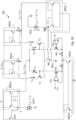
- FIG. 1 Shown in Figure 1 is a current-controlled gain amplifier 20, which has a structure of a substantially Gilbert-cell type.
- the current-controlled gain amplifier 20 substantially has a symmetrical differential structure. It includes an input stage 21 comprising a first differential branch that includes an operational amplifier OP1, the output of which is coupled to the input electrode of a MOSFET M1, in which a current I M1 flows between the drain electrode and the source electrode.
- the source electrode of the MOSFET M1 is coupled to the inverting input of the operational amplifier OP1 and, through an input resistance R I , to an input node NI, there being set, between said input node and ground, a current generator 22 for biasing the input stage 21, which receives a value of input current I bIN that is controlled via a digital signal D in , in particular a 10-bit signal, D in ⁇ 9:0> , generated by a digital-to-analog converter, not illustrated in Figure 1 , the input current I bIN having a direction exiting from the node NI towards ground GND.
- the drain electrode of the MOSFET M1 is coupled to the supply voltage Vss through a diode D1, the negative terminal of which is coupled to the drain of the MOSFET M1 and the positive terminal of which is coupled to the supply voltage Vss.
- the drain electrode of the MOSFET M1 formed on which is a base voltage V B 1 , is also coupled to an output stage 23, comprising two bipolar transistors T1 and T2, specifically to the base electrode of a first bipolar transistor T1, the collector of which is coupled to the supply voltage through an output resistance R O , whereas coupled to its emitter is a current generator 24 for biasing the output stage 23, which generates an output current I bOUT , the direction of flow of which is from the emitter to ground.
- a current I D 1 flows from the supply voltage to the drain of the MOSFET M1, while in the output resistance R O is a collector current I C 1 flows towards ground GND, the emitter current I E 1 being indicated also as flowing towards ground.
- the current-controlled gain amplifier 20 comprises a second differential branch, which includes an amplifier OP2, the output of which is coupled to the input of a MOSFET M2, in which a current I M 2 flows between the drain and the source.
- the source electrode is coupled to the inverting input of the operational amplifier OP2 and, through an input resistance R I , having a value equal to that of the other branch and hence designated by the same reference, to the input node NI, which is hence coupled to the sources of the MOSFETs M1 and M2 and to the input-current generator 22.
- the drain electrode of the MOSFET M2 is coupled to the supply voltage Vcc through a respective diode D2, similar to the diode D1 of the other branch and likewise positioned with its negative terminal, or cathode, towards the drain of the MOSFET M2 and its positive terminal, or anode, towards the supply voltage Vcc.
- the drain electrode of the MOSFET M2, on which a base voltage V B2 is set up, is also coupled to the base electrode of a second bipolar transistor T2, the collector of which is coupled to the supply voltage through a further output resistance R O , while coupled to its emitter is the output-current generator 24 and the emitter of the first transistor T1.
- a current I D 2 flows from the supply voltage to the drain of the MOSFET M2, while in the output resistance R O a collector current I C 2 flows towards ground, an emitter current I E 2 being instead indicated as flowing in the opposite direction, so that the output current I bOUT , which flows towards ground GND, is equal to the sum of the currents I E 1 and I E 2 .
- An output voltage Vout is measured between the collectors of the bipolar transistors T1 and T2, towards the bases of which base currents I B 1 and I B 2 flow.
- An input voltage Vin is applied between the non-inverting terminals of the operational amplifiers OP1 and OP2.
- the biasing conditions are that the transistors T1 and T2 are biased in the active region.
- the base currents I B 1 and I B 2 are negligible with respect to the collector currents.
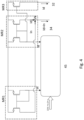
- Figure 2 is a representation of the circuit of the current-controlled gain amplifier 20, corresponding as regards circuit arrangement to that of Figure 1 , where quantities for small-signal analysis are indicated, in which the input circuit 21 and the output circuit 23 are visible in a more distinct way.
- the circuit of the current-controlled gain amplifier 20 comprises the output circuit 23, which basically comprises the pair of bipolar transistors T1, T2 and the output-current generator 23, which supplies the biasing current of the pair, i.e., the output current I bOUT , said output circuit 23 representing a differential amplification stage with emitter-coupled bipolar transistors.
- the input stage 21, comprising the components OP1, OP2, M1, M2, R I , 22, uses a circuit solution in order to provide high impedance and render the biasing current of the input transistor M1, M2 independent of the input signal.
- the function performed by the two operational amplifiers OP1 and OP2 is to bring the voltage level present on the non-inverting input directly back onto the respective source electrode of the two MOS transistors M1 and M2.
- V IN small-signal voltage
- this alters the static biasing condition and is transferred to the series of the two resistances R I , thus bringing about a variation of input current ⁇ I IN that flows in each of them, proportional to the input signal applied and obviously of opposite sign (and hence direction), in the two branches of the input stage 21:
- ⁇ I IN V IN / 2 R I
- the diodes D1 and D2 are, for example, obtained via diode-connected transistors (base shorted to the collector).
- the latter can be programmed on a scale of different values keeping fixed and constant the biasing current of the output stage 23 I bOUT and varying/ controlling the biasing current of the input stage I bIN using a current generator controlled by a digital-to-analog converter (DAC).
- a I ⁇ I OUTdiff 2
- the amplification circuit with current-controlled gain 20 described with reference to Figures 1 and 2 provides a variable-gain amplifier with constant input and output biasing.
- the above circuit in general presents a criticality as regards matching of the currents.
- the input current I bIN must range from one hundredth of the value to the value of the output current I bOUT , so that the ratio between the currents I bOUT I LSB should be precise and kept constant in time, i.e., independent of the any disturbance during production and operation (temperature variation, process spread, etc.).
- Further criticalities described in greater detail with reference to the embodiment of Figure 11 , may regard the beta factor.
- the solution described thus refers to a variable-gain amplifier with constant output biasing that divides the input and output biasing currents as a function of the gain to be obtained.
- Constant-current output biasing presents the advantage of maintaining the stage downstream always in the same operating conditions, thus preventing, for example, problems of common-mode variation that might disturb the operating point.
- a biasing of the input stage is carried out with a denominator current of programmable value I d .
- Figure 3 hence shows an embodiment 30 of an amplification circuit with current-controlled gain that corresponds for the most part to the amplification circuit 20.
- a programmable current generator 32 is provided, which generates the denominator current of programmable value I d under the control of a signal of a DAC (not illustrated in Figure 3 ).
- the amplification circuit 30 represented is topologically similar to the amplification circuit 20 and is distinguished by the choice of the biasing currents of the input and output stages. It is hence possible to proceed with biasing and small-signal analyses similar to those developed previously for the amplification circuit 20.
- the input stage designated by 31 in Figure 3 , uses a circuit solution to render the biasing current of the input transistor independent of the input signal.
- the output biasing depends upon the sum current I d + I n .
- the gain is a function of the denominator current I d and the numerator current I n . If the sum of the currents, or sum current, I d + I n is constant, the output stage 33 is biased always in the same way. This makes it possible to get the stage downstream of the circuit 30 to function at a constant biasing independent of the gain.
- the denominator current I d is mirrored by a branch of the differential DAC, and the sum current I d + I n is the sum of the two branches.
- the currents I d and I d + I n can be obtained from components that are the same as one another and have the same temperature dependence.
- the gain of the Gilbert cell depends upon the collector currents of the bipolar transistors (the diodes may also be implemented using bipolar transistors). In the configuration of the circuit 30, these currents are not controlled because they are imposed by the emitter and the cathode of the diode. Hence, for applications that require gains that are very precise and high (high current ratio ( I d + I n )/ I d , low currents I d )the circuit 30 may present a limitation in precision.
- FIG. 4 illustrated in Figure 4 is an embodiment 40, which corresponds to the embodiment 30 but in which a digital-to-analog converter (DAC) 45 is illustrated that supplies the denominator current I d and the numerator current I n .
- DAC digital-to-analog converter
- the DAC 45 comprises an input for an n-bit digital datum D in ⁇ n...0> and supplies at output the complementary current I n to a first current mirror MR1 and the denominator current of programmable value I d to a second current mirror MR2.
- the first current mirror MR1 mirrors the current I n towards a sum node SN, flowing into which is also the current mirrored by the second current mirror MR2, thus obtaining the current I d + I n , and consequently providing the output biasing-current generator 34, whereas a current mirror in parallel MR3 mirrors the current I d towards a further output, consequently providing the input biasing-current generator 32.
- the same circuit that enables selection of the gain provides matching between the ratio of the currents that determine the gain.
- the DAC 45 is linear, with linear variation of gain, where there is, for example:
- Figure 5 shows an embodiment of the DAC 45 of a current-steering type, in which a plurality of current mirrors is formed, where one branch is constituted by the diode-connected MOSFET M0, with aspect ratio W/L, in which a current I ref /2 flows, connected in parallel to which are n MOSFETs M1, ..., Mn with aspect ratio decreasing from W/L; W to W/2 n-1 L; i.e., each successive transistor determines an output current halved from I ref /2 to I ref /2 n .
- the aforesaid DAC 45 is of a binary type in so far as the output currents have values according to powers of 2 distinct according to the bit selected.
- Each of the aforesaid currents can be connected, via a respective switch Dn-1, ..., D0, either to the output terminal on which the current I n is picked up, or else to the output terminal on which the current I d is picked up.
- the digital input D in corresponding to the desired gain determines the state of each of the switches D0, ..., Dn-1 and hence the level of the two output currents I n and I d . It may be noted how, irrespective of the code of the digital input D in , the sum of the two output currents remains constant and equal to I ref , the gain being given by the ratio of I d + I n over I d . It follows that any imprecision/imperfection within the DAC 45 with respect to ideality is transferred proportionally to the numerator and to the denominator of the gain, thus achieving a substantial immunity of the latter with respect to the imperfections/imprecisions during operation of the circuit and/or due to the production process.
- FIG. 6A shows a block diagram of a biasing subsystem of the output stage 50C
- a circuit is used for biasing the transistors T1 and T2 that comprises a reference current I refC that is to be forced as the same collector current I C 1 , I C 2 , on the two transistors T1 and T2, supplied by a generator (not illustrated), which is sent to a comparison node NCC, where, in particular, a subtraction is made, to obtain an error err C (difference) between an effective collector current I C 1 , I C 2 , and the reference current I refC , said error err C being supplied to a block that applies a gain K C ( s ) , which is a transfer function where s is the variable in the Laplace domain, to amplify said error err C .
- the output of the gain block K C ( s ) is supplied as control signal to a current generator 501C, which is hence controlled by the amplified error err C and which is coupled to the emitters of T1 and T2 and simultaneously forces the emitter current I E 1 , I E 2 , on the two transistors T1 and T2 so as to bring the error to zero.
- the solution described herein envisages, in some embodiments, forcing an appropriate biasing current of the input stage in such a way as to guarantee the diode current I D 1 , I D 2 required on each diode D1, D2.
- a reference current I refD that is to be forced in each of the two diodes D1, D2 is supplied to a comparison node NCD to obtain the error err D (difference) between the effective diode current I D and the reference current I refD , said error err D being supplied to a block that applies a gain K D ( s ), which is a transfer function where s is the variable in the Laplace domain, to amplify the above error err D .
- the output of the gain block K D ( s ), is supplied as control signal to a current generator 501D, which is hence controlled by the error err D amplified, that forces the biasing current I biasIN into each of the two branches of the input stage 21 or 31 in such a way as to bring the error err D to zero.
- the other elements of the circuits 50C and 50D of Figures 6A and 6B are illustrated explicitly, in particular, the reference-current generators 502C and 502D that generate the reference currents I refC ,I refD respectively, which are sent to the comparison nodes NCC, NCD in blocks 50'C, 50'D.
- the collector currents I C 1 and I C 2 are sent at input to the block 50'C (coupled to the collector electrodes of the transistors T1 and T2), whereas the diode currents I D 1 and I D 2 are sent at input to the block 50'D (which is coupled to their anodes).
- the controlled current generator 501C of the biasing circuit of the output stage 50C corresponds to the biasing-current generator 24 or 34 of the output stage 23 or 33, which, in this case, becomes a current generator controlled by the output of the block 50'C, i.e., err C ⁇ K C ( s ) .
- the controlled current generator 501C of the diode-biasing circuit 50D corresponds to the biasing-current generator 22 or 32 of the input stage 21 or 31, which in this case becomes a current generator controlled by the output of the block 50'D, i.e., err D ⁇ K D ( s ).
- Figure 8 illustrates a possible implementation of the input-stage biasing loop 50C.
- the circuit 50C is represented for the transistor T, which may be either T1 or T2.
- the collector current I C from the collector is mirrored by a current mirror MR1C, formed by a diode-connected MOSFET M4 and a MOSFET M5, the transistors, which are p-channel transistors, having their sources coupled to the supply voltage V dd , into a comparison branch at input to a second current mirror MR2C, formed by a diode-connected MOSFET M1 and a MOSFET M2, the transistors, which are n-channel transistors, having their sources coupled to the ground voltage.
- Coupled to the node NCC is the gate of a MOSFET M3 representing the current-controlled generator 501C, the drain of which is coupled to the emitter of the transistor T.
- a series RC circuit, Cc + Rc is set in parallel to the gate, thus bringing about a control voltage drop ⁇ V DS 2 that controls the MOSFET M3, which represents the current-controlled generator 501C.
- the collector current I C varies with respect to the reference current I refC by a variation ⁇ i C it may be seen how this reflects upon the control voltage ⁇ V DS 2 .
- the analysis can be developed as described in what follows.
- the transistor M3 functions as a voltage-controlled current generator, in particular controlled by the voltage V DS 2 , thus providing the generator 501C of Figures 6A and 7 .
- i 3 g m 2 Rc + 1 SCc gm 3 ⁇ i 1 g m 1
- controlled current ⁇ i 3 which is proportional to the error/perturbation signal ⁇ i 1 according to the gain factor, which is basically equal, the MOSFETs being all the same, to g m r DS >> 10 and has a sign opposite to that of the perturbation so that the loop 50C will compensate the error and progressively tend to bring it to zero.
- the circuit 50C is represented for the diode D, which may be either D1 or D2.
- the diode current I D from the cathode of the diode D is mirrored by a current mirror MR2D, formed by a diode-connected MOSFET M1D and a MOSFET M2D, which are p-channel MOSFETs with sources connected to the supply voltage.
- a current mirror MR2D formed by a diode-connected MOSFET M1D and a MOSFET M2D, which are p-channel MOSFETs with sources connected to the supply voltage.
- an output branch from the above node NCD yields a current that is the difference between the two currents, and hence the current error err c .
- Coupled to the node NCD is the gate of a MOSFET M3D, which represents the current-controlled generator 501D, the drain of which is coupled to the cathode of the diode D through a current mirror MR1C, formed by a diode-connected MOSFET M4D and a MOSFET M5D, the transistors, which are n-channel transistors, having their sources coupled to the ground voltage.
- the source of the MOSFET M3D which is a p-channel MOSFET, is connected to the supply voltage, while the drain is connected to the drain of the NOSFET M4D.
- a series RC circuit, Cc + Rc, is set in parallel to the gate of the transistor M3D, between the node NCD and ground, bringing about on itself a control voltage drop that controls the MOSFET M3D that represents the current-controlled generator 501D.
- FIG 10 illustrated in Figure 10 is an overall diagram of the circuit 50 of Figure 7 , with the implementations of Figures 8 and 9 , where the biasing of the diodes D1 and D2 is fixed by the denominator current I d .
- a respective current mirror MR1C is used on the respective collector to convey the collector currents at input to the mirror MR2C.
- a node designated by NA corresponding to the comparison node NCD, which is subject to high gain, imposes a current equal to the denominator current I d through the loop 50D.
- the node NB corresponding to the comparison node NCC, which subject to high gain, imposes a current equal to the sum current I d + I n through the loop 50C.
- the output biasing depends upon the sum current I d + I n .
- the transconductance g m of the transistors T1, T2 depends only upon the collector currents, which are fixed and independent of the beta factor ⁇ of the transistors T1, T2 used.
- the amplification circuit with current-controlled gain 30, 40 or 50 may present a further criticality, due to a gain error.
- the factor ⁇ of the transistors which are bipolar transistors, for example BCDs (Bipolar CMOS DMOS), may be very low (for example, between 30 and 50).
- the base current of the transistors T1 and T2 subtracts current from the diodes D1 and D2, which hence have a current lower than I bIN /2 , leading to a gain error that depends upon the factor ⁇ , as shown by the foregoing equations.
- the factor ⁇ markedly depends upon temperature, as well as upon the collector current itself, it emerges that the expected gain could undergo substantial variations during the service life of the device.
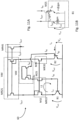
- Figure 11A shows a further circuit 60 for recovery and compensation of the base current of the bipolar transistors T, T1, and T2, which also enables compensation of the difference of the base currents due to an unbalancing of the input signal.
- the Gilbert cell with bipolar transistors presents in fact intrinsically a limit due to the base current, I B in Figure 1 , of the bipolar transistors due to the finite beta factor.
- beta factor ⁇ may assume values lower than 100.
- the base currents I B 1 , I B 2 may differ between the two transistors T1, T2 when a differential signal is applied, giving rise to behaviours that are not easily predictable.
- a circuit 60 is applied to the amplifier with controlled gain, in particular current-controlled gain, 20, 30, 40, 50, to compensate for the individual base currents of the bipolar transistors T1 and T2.
- the transistor B2 represents each individual transistor of the output stage 23, whether T1 or T2, which is consequently traversed by the output current I OUT , which corresponds to the collector current I C 1 or I C 2 of the bipolar transistor T1 or T2 of which the base current is to be compensated so as to provide a so-called super-beta virtual transistor.
- the compensation circuit designated by 60 comprises a reference component that normally is used as amplifier, the transistor B2 that corresponds to T1 or T2, and a supporting component, the transistor B1 forced to work in the same working conditions as the transistor B2, a loop L1 used to force the operating condition of the supporting transistor B1, which comprises the transistor B1, and a current mirror MR1S, comprising MOSFETs M1S (which is diode-connected) and M2S.
- the source electrode of the transistor M1S is coupled to the emitter of the supporting transistor B1, and the gate of the supporting transistor B1 is coupled to the source of M2S.
- the transistor B1 (or T1, T2) receives on its collector a copy of the output current of the transistor B2, I OUT , via a p-channel current mirror MR2S coupled to the branch in which there flows the current I OUT that traverses the reference transistor B2 and as output the base current I B 1 which in turn is mirrored on the base of the transistor B2 by a p-channel current mirror MR3S.
- a mirror M4RS in parallel to the current mirror M3RS supplies the output current of the amplifier.
- the base current I B 1 of the transistor B1 is linked to the collector current I C 1 of the transistor B1 via the beta factor of the transistor B1.
- the collector of the supporting transistor B1 represents a comparison node (with high impedance and hence high gain), between the current I OUT and its collector current I C 1 .
- the difference between these currents sets up a collector-to-emitter voltage V CE 1 on the collector-to-emitter resistance R CE 1 of the transistor B1 (which has a normally very high value), the above collector-to-emitter voltage V GE 1 being used for controlling the base current I B 1 of the transistor B1 via the MOSFET M2S, thus forming a negative loop with inversion of sign on the collector of the transistor B1.
- the MOSFET M2S forces a base current such that the collector current I C 1 is equal to the current I OUT , thanks to the negative loop comprising the base current I B 1 , the collector current I C 1 , and the collector-to-emitter voltage V CE 1 of the transistor B1.
- the collector of the transistor B1 thus represents a gain point.
- the wide operating dynamics is guaranteed by the fact that the bipolar transistors B1 and B2 work with a collector-to-emitter voltage V CE equal to the base-to-emitter voltage V BE .
- the supporting transistor B1 is represented by the small-signal model.
- r is the dynamic input resistance traversed by the base current I B 1 coming from the transistor M2S and is, in particular, equal to ⁇ / g m .
- a current-controlled generator g m ⁇ V BE , I C 1 , between the collector and the emitter has, in parallel between the collector and ground, the collector-to-emitter resistance r CE 1 .
- the compensation circuit 60 applied to the transistors T1 and T2 of the circuits 30, 40, 50 affords the following features:
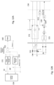
- an ultrasonic obstacle detector 150 comprising a pulse transmitter 152, which drives, via its own pulses, a piezoelectric transducer 152, which is an ultrasound transceiver; i.e., it both transmits ultrasounds and receives them, for example via a piezoelectric membrane, and operates under the control of transmission-control pulses TP sent by a control circuit, to emit ultrasound pulses, i.e., pressure-wave pulses.
- an object 160 at a distance L which reflects the ultrasound waves associated to the ultrasound pulses, which are then detected by the piezoelectric transducer 152 itself, the output of which is sent to a receiver circuit 153.
- the receiver circuit 153 then sends reception-control pulses RP to the control circuit CM, which measures the difference in time T between the transmission-control pulses TP and the reception-control pulses TP.
- the difference in time T is also known as time of flight. Knowing the rate of propagation of the ultrasound pulses, it is possible to determine the distance L.
- FIG 12B shows a partial block diagram of the ultrasonic obstacle detector 150, which comprises the transducer 152, which is represented schematically as a parallel RC circuit, which is driven by the pulse transmitter 51, to which it is coupled via a transformer.
- the transducer 152 is also coupled in reception to the receiver circuit 153, a receiver of the ultrasound sensor, in its turn an analog-to-digital converter (ADC) 130.
- ADC analog-to-digital converter
- an ultrasound signal received RS which is an analog differential signal
- a signal chain comprising a clamp circuit CP, followed by a low-noise amplifier LNA and then by a variable-gain amplifier VGA, the gain of which is controlled by the control module CM through a digital-to-analog converter DC1 and which supplies a differential voltage Vdiff at input to the ADC 130.
- Ultrasonic obstacle-dectection systems must manage problems of environmental interference and of detection systems of adjacent vehicles.
- Wind and rain attenuate and disturb the transmitted signal.
- Pulses coming from adjacent vehicles may give rise to false diagnostics and detection. It is possible to modulate the transmitted signal (above all for distances greater than one metre) to render the latter recognizable during reception. It is difficult, in particular, to provide a system capable of recognizing simultaneously objects that are far away and nearby. Detecting signals reflected by nearby and distant obstacles requires a wide reception range.
- a gain control like that of the VGA of Figure 12B enables conversion of the signal received with an ADC with a conversion range that is small than what is actually necessary.
- circuit-arrangement solution described makes it possible to obtain a variable-gain stage with high gain precision. Moreover, a compact architecture is achieved using a differential current DAC.
Landscapes
- Engineering & Computer Science (AREA)
- Radar, Positioning & Navigation (AREA)
- Remote Sensing (AREA)
- Physics & Mathematics (AREA)
- Computer Networks & Wireless Communication (AREA)
- General Physics & Mathematics (AREA)
- Power Engineering (AREA)
- Acoustics & Sound (AREA)
- Amplifiers (AREA)
Abstract
said circuit arrangement being configured for controlling a gain between the input and the output by controlling the values of input and output biasing current;
said circuit arrangement (30) being configured for supplying a first reference current ( Id ) and a second reference current ( In ) having complementary values such that their sum is constant, the value of said input biasing current (IbIN ) corresponding to the first reference current ( Id ), and the output biasing current ( IbOUT ) corresponding to the sum ( Id + In ) of said first reference current (Id ) and said second reference current ( In ).
Description
- The embodiments of the present disclosure relate to amplification techniques with current-controlled gain.
- The embodiments of the present disclosure refer in particular to ultrasonic obstacle detectors.
- Variable-gain amplifiers are known, which vary their own gain on the basis of a control quantity. Such variable-gain amplifiers are widely used in many fields of electronics, amongst which telecommunications, processing of audio signals, and detection via sensors, for example, ultrasonic obstacle detectors.
- A known and simple way for implementing a variable gain is to use variable components on the feedback branch of a voltage amplifier, which, as is known, comprises a variable resistance on the input terminal, for example an inverting terminal, and a variable feedback resistance between the output and the input. The gain depends upon the ratio of two resistances and hence upon their value: by varying either one or both, the gain varies. It is very difficult, however, to obtain a ratio of resistances independent of the value of such resistances. Passing from very low gains to very high gains is difficult. The selection components typically used (for example, MOSFETs) for imposing the value of gain may have on-state resistances, Ron, comparable with those of the variable resistors, thus jeopardising their precision.
- Circuits are known that solve the problem of gain accuracy, generating a current starting from another current via cells with two differential pairs of transistors, one for the input and one for the output, cross-coupled, i.e., the transistors of one and the same branch in each differential pair have their base in common. The outputs are, for example, connected to the inputs of an amplifier, the outputs of which are connected to the common base electrodes. An example of the aforesaid variable-gain amplifier circuit may be found, for example, in the URL https://www.analog.com/media/en/technical-documentation/data-sheets/AD8338.pdf, page 12 (Figure 40). This type of circuit makes it possible to obtain a high gain precision. In this case, there is a biasing current (both at input and at output) depending upon the gain selected. Similar solutions hence render the performance of the circuit in terms of biasing dependent upon the gain. Moreover, there is a gain error that depends upon the mismatches of the beta factors β of the bipolar transistors of the differential pairs.
- On the basis of the foregoing description, there is felt the need for solutions that overcome one or more of the drawbacks outlined previously.
- According to one or more embodiments, the above object is achieved by means of a circuit having the characteristics set forth specifically in the ensuing claims. The embodiments moreover refer to a corresponding method and to an ultrasonic obstacle detector.
- The claims form an integral part of the technical teaching of the disclosure provided herein.
- As mentioned previously, the present disclosure provides solutions regarding circuit arrangement of an amplifier with current-controlled gain, said circuit arrangement having a symmetrical differential structure, comprising a differential input stage, which includes, on each differential branch, an input transistor, in particular a MOSFET, coupled, in particular through an input resistance, to an input node, there being set between said input node and ground a current generator for biasing the input stage that supplies said input stage being configured for operating with a constant input biasing, an input voltage being applied between the inputs of the input transistors, a drain electrode of the input transistor being coupled to the supply voltage through a respective diode, as well as to a differential output amplification stage having bipolar transistors with coupled emitters, there being coupled to said emitters a current generator for biasing the output stage which generates an output current and comprises, on each differential branch, a bipolar transistor biased in the active region, the base electrode of which is coupled to the drain electrode of the input transistor and the collector electrode of which is coupled to the supply voltage, while coupled to its emitter electrode is a current generator for biasing the output stage which generates an output current, an output voltage being drawn from between the collectors of the bipolar transistors, said output stage being configured with constant output biasing,
- said circuit arrangement being configured for controlling a gain between the input and the output by controlling the values of input and output biasing current;
- said circuit arrangement being configured for supplying a first reference current and a second reference current having complementary values such that their sum is constant, the value of said input biasing current corresponding to the first reference current, and the output biasing current corresponding to the sum of said first reference current and said second reference current.
- In variant embodiments, said circuit arrangement is configured for controlling a gain between the input voltage and the output voltage, keeping the biasing current of the output stage at a constant fixed value and controlling the value of the biasing current of the input stage, said input-stage biasing-current generator being controlled, in particular, via a digital signal generated by a digital-to-analog converter.
- In variant embodiments, said differential output amplification stage with emitter-coupled bipolar transistors, comprises, on each differential branch, a bipolar transistor biased in the active region, the base electrode of which is coupled to the drain electrode of the input transistor and the collector electrode of which is coupled to the supply voltage, while coupled to its emitter electrode is a current generator for biasing the output stage, which generates an output current.
- In variant embodiments, each differential branch comprises an operational amplifier, the output of which is coupled to the control input, in particular the gate, of the input transistor, an output of which, in particular the source, is coupled to the inverting input of the respective operational amplifier, the input voltage being applied between the non-inverting inputs of the operational amplifiers.
- In variant embodiments, said first reference current and said second reference current are supplied by a differential digital-to-analog converter.
- In variant embodiments, said circuit arrangement comprises a further circuit for biasing the output stage comprising a control loop configured for controlling said output biasing-current generator in such a way as to regulate the collector current of the bipolar transistor so that it follows a reference value of collector current.
- In variant embodiments, said circuit arrangement comprises a further circuit for biasing the diodes, comprising a control loop configured for controlling said input biasing-current generator in such a way as to regulate the current in the diodes so that it follows a reference value of diode current.
- In variant embodiments, said bipolar transistors are comprised in a circuit arrangement configured for recovering and compensating the base current of said bipolar transistors.
- In variant embodiments, said circuit arrangement configured for recovering and compensating the base current of said bipolar transistors comprises said output bipolar transistor and a supporting bipolar transistor associated to a control loop, which comprises a current mirror that receives at input the output current of the input bipolar transistor and supplies at output to the supporting bipolar transistor said current as base current, said base current being mirrored in the base of the output bipolar transistor.
- The present disclosure also provides solutions that regard an ultrasonic obstacle detector including a receiver comprising a circuit arrangement of an amplifier with current-controlled gain according to embodiments.
- The present disclosure also provides solutions that regard a method for controlling a circuit arrangement of an amplifier with current-controlled gain according to embodiments, comprising controlling a gain between the input and the output by controlling the values of the input and output biasing current.
- In variant embodiments, the method comprises controlling a gain between the input voltage and the output voltage, keeping the biasing current of the output stage at a constant fixed value and controlling the value of the biasing current of the input stage, said input-stage biasing-current generator being controlled, in particular, via a digital signal generated by a digital-to-analog converter.
- In variant embodiments, the method comprises supplying a first reference current and a second reference current of complementary values such that their sum is constant, the value of said input biasing current corresponding to the first reference current, and the output biasing current corresponding to the sum of said first reference current and said second reference current, in particular said first reference current and said second reference current being supplied by a differential digital-to-analog converter.
- Embodiments of the present disclosure will now be described with reference to the annexed drawings, which are provided purely by way of non-limiting example, and in which:
-
Figure 1 is a schematic illustration of a circuit arrangement according to first embodiments; -
Figure 2 is a schematic illustration of the circuit arrangement ofFigure 1 according to embodiments with further details of implementation; -
Figure 3 is a schematic illustration of a circuit arrangement according to embodiments; -
Figure 4 is a schematic illustration of a circuit used by the circuit arrangement according to the foregoing embodiments; -
Figure 5 illustrates a diagram of implementation of the circuit ofFigure 4 ; -
Figure 6A and 6B illustrate additional biasing circuits that can be used in a circuit arrangement according to embodiments; -
Figure 7 is a schematic illustration of a circuit arrangement according to embodiments that is associated to the additional biasing circuits ofFigure 6A and 6B ; -
Figure 8 shows a detailed diagram of the additional circuit ofFigure 6A ; -
Figure 9 shows a detailed diagram of the additional circuit ofFigure 6B ; -
Figure 10 illustrates a detailed diagram of a circuit arrangement according to embodiments that is associated to said additional circuits ofFigures 8 and9 ; -
Figure 11A is a schematic illustration of a compensation circuit that can be associated to the circuit arrangement according to embodiments; -
Figure 11B is a schematic illustration of a detail of the above compensation circuit; -
Figure 12A is a schematic illustration of an ultrasonic obstacle detector comprising the circuit arrangement described herein; and -
Figure 12B illustrates a partial detailed block diagram of the detector ofFigure 12A . - In the ensuing description, numerous specific details are illustrated in order to enable an in-depth understanding of embodiments. The embodiments may be implemented without one or more of the specific details or with other methods, components, materials, etc. In other cases, well-known operations, materials or structures are not illustrated or described in detail so that certain aspects of the embodiments will not be obscured.
- Reference to "an embodiment" or "one embodiment" in the framework of the present disclosure is intended to indicate that a particular configuration, structure, or characteristic described with reference to the embodiment is comprised in at least one embodiment. Hence, phrases such as "in an embodiment" or "in one embodiment" or the like that may be present in various points of the present description do not necessarily all refer to one and the same embodiment. Moreover, particular conformations, structures, or characteristics may be combined in any adequate way in one or more embodiments.
- The references used herein are provided merely for convenience and hence do not define the sphere of protection or the scope of the embodiments.
- Components, elements, or parts that will be described with reference to one drawing are designated, in the subsequent drawings, by the same references as those used in that drawing; the description of the aforesaid elements already described will not be subsequently repeated in order not to overburden the present detailed description.
- Shown in
Figure 1 is a current-controlledgain amplifier 20, which has a structure of a substantially Gilbert-cell type. - The current-controlled
gain amplifier 20 substantially has a symmetrical differential structure. It includes aninput stage 21 comprising a first differential branch that includes an operational amplifier OP1, the output of which is coupled to the input electrode of a MOSFET M1, in which a current IM1 flows between the drain electrode and the source electrode. The source electrode of the MOSFET M1 is coupled to the inverting input of the operational amplifier OP1 and, through an input resistance RI , to an input node NI, there being set, between said input node and ground, acurrent generator 22 for biasing theinput stage 21, which receives a value of input current IbIN that is controlled via a digital signal Din, in particular a 10-bit signal, D in<9:0> , generated by a digital-to-analog converter, not illustrated inFigure 1 , the input current IbIN having a direction exiting from the node NI towards ground GND. The drain electrode of the MOSFET M1 is coupled to the supply voltage Vss through a diode D1, the negative terminal of which is coupled to the drain of the MOSFET M1 and the positive terminal of which is coupled to the supply voltage Vss. The drain electrode of the MOSFET M1, formed on which is a base voltage V B1, is also coupled to anoutput stage 23, comprising two bipolar transistors T1 and T2, specifically to the base electrode of a first bipolar transistor T1, the collector of which is coupled to the supply voltage through an output resistance RO , whereas coupled to its emitter is acurrent generator 24 for biasing theoutput stage 23, which generates an output current IbOUT, the direction of flow of which is from the emitter to ground. In the diode D1 is a current I D1 flows from the supply voltage to the drain of the MOSFET M1, while in the output resistance RO is a collector current I C1 flows towards ground GND, the emitter current I E1 being indicated also as flowing towards ground. - Symmetrically, the current-controlled
gain amplifier 20 comprises a second differential branch, which includes an amplifier OP2, the output of which is coupled to the input of a MOSFET M2, in which a current I M2 flows between the drain and the source. The source electrode is coupled to the inverting input of the operational amplifier OP2 and, through an input resistance RI , having a value equal to that of the other branch and hence designated by the same reference, to the input node NI, which is hence coupled to the sources of the MOSFETs M1 and M2 and to the input-current generator 22. The drain electrode of the MOSFET M2 is coupled to the supply voltage Vcc through a respective diode D2, similar to the diode D1 of the other branch and likewise positioned with its negative terminal, or cathode, towards the drain of the MOSFET M2 and its positive terminal, or anode, towards the supply voltage Vcc. - The drain electrode of the MOSFET M2, on which a base voltage VB2 is set up, is also coupled to the base electrode of a second bipolar transistor T2, the collector of which is coupled to the supply voltage through a further output resistance RO , while coupled to its emitter is the output-
current generator 24 and the emitter of the first transistor T1. In the diode D2 a current I D2 flows from the supply voltage to the drain of the MOSFET M2, while in the output resistance RO a collector current I C2 flows towards ground, an emitter current I E2 being instead indicated as flowing in the opposite direction, so that the output current IbOUT, which flows towards ground GND, is equal to the sum of the currents I E1 and I E2. - An output voltage Vout is measured between the collectors of the bipolar transistors T1 and T2, towards the bases of which base currents I B1 and I B2 flow.
- An input voltage Vin is applied between the non-inverting terminals of the operational amplifiers OP1 and OP2.
- As regards biasing of the
circuit 20 we have the following situation. - Recalling that IC = -IE - IB , the biasing conditions are that the transistors T1 and T2 are biased in the active region. To a first approximation, the base currents I B 1 and I B 2 are negligible with respect to the collector currents.
- By symmetry,


- This but for the contribution of the current injected into the base of each transistor.
- As regards the transistors M1 and M2, by symmetry, we have

- As in the case of biasing of the bipolar transistors T1 and T2, it is assumed that the base current subtracted from the biasing current of the diodes D1 and D2 is negligible, and hence


-
Figure 2 is a representation of the circuit of the current-controlledgain amplifier 20, corresponding as regards circuit arrangement to that ofFigure 1 , where quantities for small-signal analysis are indicated, in which theinput circuit 21 and theoutput circuit 23 are visible in a more distinct way. - Hence, the circuit of the current-controlled
gain amplifier 20 comprises theoutput circuit 23, which basically comprises the pair of bipolar transistors T1, T2 and the output-current generator 23, which supplies the biasing current of the pair, i.e., the output current IbOUT, saidoutput circuit 23 representing a differential amplification stage with emitter-coupled bipolar transistors. For this structure, in small-signal regime, the relation between the variation ΔVBdiff of the input signal, which is the difference between the voltages on the bases of the two transistors, VBdiff = V B1 - V B2 , and the variation of the output signal, which is the difference between the voltages on the collectors, VOUT = V C1 - V C2 , is the following:
- The parameter gmT = dIC /dVBE = IC /VT represents the transconductance of each of the two bipolar transistors T1 and T2 in the operating point determined by the biasing collector current IC , and, given what has been said previously, is the same for both and is approximately equal to:

- The
input stage 21, comprising the components OP1, OP2, M1, M2, RI , 22, uses a circuit solution in order to provide high impedance and render the biasing current of the input transistor M1, M2 independent of the input signal. - The function performed by the two operational amplifiers OP1 and OP2 is to bring the voltage level present on the non-inverting input directly back onto the respective source electrode of the two MOS transistors M1 and M2. As a result of this function, once again analysing the circuit in the small-signal regime, when a (small-signal) voltage VIN is imposed on the input of the circuit, this alters the static biasing condition and is transferred to the series of the two resistances RI , thus bringing about a variation of input current ΔIIN that flows in each of them, proportional to the input signal applied and obviously of opposite sign (and hence direction), in the two branches of the input stage 21:

- As regards calculation of the gain in small-signal regime, the diodes D1 and D2 are, for example, obtained via diode-connected transistors (base shorted to the collector).
- As is known, the transconductance of the two diodes D1 and D2, g mD1 , g mD2, is
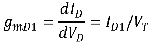

- In the case of the amplification circuit with current-controlled
gain 20 described, the above two diodes D1 and D2 are the same as one another and biased in the same way so that the transconductances are identical to one another and (approximately) equal to
- Proceeding with the analysis, as a result of the variation of the input current ΔIIN in each of the two branches there is brought about a variation of the current ΔI D1 ≅ ΔIIN and ΔI D2 ≅ - ΔIIN that flows in the respective diodes D1 and D2 (but for the base currents absorbed by the transistors T1 and T2), which, in turn, as a result of the voltage-current characteristic of the diode, results in a variation of voltage on the bases of the respective transistors T1, T2, namely, ΔV B1 ≅ -ΔIIN / gmD and ΔV B2 ≅ - ΔIin / gmD. Hence, we have


- Substituting the above in the equation ΔVOUTdiff = -gmT R 0 ΔVBdiff, we obtain

- As may be noted from the formula of the voltage gain AV , the latter can be programmed on a scale of different values keeping fixed and constant the biasing current of the output stage 23 IbOUT and varying/ controlling the biasing current of the input stage IbIN using a current generator controlled by a digital-to-analog converter (DAC).

- The current gain is instead

- As has been said, this analysis has been made on the assumption of negligible base currents. But if also these were taken into account, it can be shown that a more accurate relation between the input-current variation ΔIIN and the output-current variation ΔIOUT (and hence the current gain) is


- The amplification circuit with current-controlled
gain 20 described with reference toFigures 1 and2 provides a variable-gain amplifier with constant input and output biasing. - The above circuit in general presents a criticality as regards matching of the currents. The input current IbIN must range from one hundredth of the value to the value of the output current IbOUT, so that the ratio between the currents

Figure 11 , may regard the beta factor. - Hence, with reference to
Figure 3 an embodiment is described for implementing a function of amplifier used for equalizing the output signal as the input signal varies, via gain adjustment. - The solution described thus refers to a variable-gain amplifier with constant output biasing that divides the input and output biasing currents as a function of the gain to be obtained.
- Constant-current output biasing presents the advantage of maintaining the stage downstream always in the same operating conditions, thus preventing, for example, problems of common-mode variation that might disturb the operating point.
- In particular, as illustrated in
Figure 3 , a biasing of the input stage is carried out with a denominator current of programmable value Id . Biasing of the output stage is carried out with a constant current IbOUT, the value of which is, however, obtained from the sum of two current contributions, one of which is a first reference current, or denominator current, of programmable value Id, and the other is a second reference current, or numerator current In , i.e., of a value complementary with respect to the constant current IbOUT, namely, such that IbOUT = Id + In. -
Figure 3 hence shows anembodiment 30 of an amplification circuit with current-controlled gain that corresponds for the most part to theamplification circuit 20. Instead of thegenerator 22, however, a programmablecurrent generator 32 is provided, which generates the denominator current of programmable value Id under the control of a signal of a DAC (not illustrated inFigure 3 ). - Instead of the
current generator 24, acurrent generator 34 is provided, which generates a current of constant value obtained from the sum of two current contributions, one of which is the denominator current of programmable value Id and the other is the complementary numerator current In , such that IbOUT = Id + In , which is a constant current. - As has been said, the
amplification circuit 30 represented is topologically similar to theamplification circuit 20 and is distinguished by the choice of the biasing currents of the input and output stages. It is hence possible to proceed with biasing and small-signal analyses similar to those developed previously for theamplification circuit 20. - As has been said, the input stage, designated by 31 in
Figure 3 , uses a circuit solution to render the biasing current of the input transistor independent of the input signal. - In small-signal regime, if ΔIIN is the variation of the current in the individual branch of the
input stage 31 that flows in each resistance RI and is induced by the variation of the input signal VIN and if ΔIdiffout = Δ(I C1 - I C2) is the variation of the differential output current ( I C1 - I C2 ) induced once again by the input signal VIN, we can write the relation between these two variations of currents, thus determining the current gain. - The gain of the
circuit 30 defined as ΔIdiffout over 2ΔIIN can be obtained from the following:

- The expression of the current gain is thus

- Hence, the output biasing depends upon the sum current Id + In .
- The gain is a function of the denominator current Id and the numerator current In. If the sum of the currents, or sum current, Id + In is constant, the
output stage 33 is biased always in the same way. This makes it possible to get the stage downstream of thecircuit 30 to function at a constant biasing independent of the gain. - It is thus envisaged to use, in association with the
amplification circuit 30, a differential DAC, the output currents of which are complementary and the sum of which is constant, i.e., the output currents correspond to the currents Id and In used by thecircuit 30. - The denominator current Id is mirrored by a branch of the differential DAC, and the sum current Id + In is the sum of the two branches. The currents Id and Id + In can be obtained from components that are the same as one another and have the same temperature dependence.
- The gain of the Gilbert cell depends upon the collector currents of the bipolar transistors (the diodes may also be implemented using bipolar transistors). In the configuration of the
circuit 30, these currents are not controlled because they are imposed by the emitter and the cathode of the diode. Hence, for applications that require gains that are very precise and high (high current ratio ( Id + In )/ Id , low currents Id )thecircuit 30 may present a limitation in precision. - To solve the aforesaid problem, illustrated in
Figure 4 is an embodiment 40, which corresponds to theembodiment 30 but in which a digital-to-analog converter (DAC) 45 is illustrated that supplies the denominator current Id and the numerator current In. - The
DAC 45 comprises an input for an n-bit digital datum Din <n...0> and supplies at output the complementary current In to a first current mirror MR1 and the denominator current of programmable value Id to a second current mirror MR2. The first current mirror MR1 mirrors the current In towards a sum node SN, flowing into which is also the current mirrored by the second current mirror MR2, thus obtaining the current Id + In , and consequently providing the output biasing-current generator 34, whereas a current mirror in parallel MR3 mirrors the current Id towards a further output, consequently providing the input biasing-current generator 32. - The same circuit that enables selection of the gain provides matching between the ratio of the currents that determine the gain.
- The
DAC 45 is linear, with linear variation of gain, where there is, for example: - In = (( D in<n-1:0> )/2n) Iref
- Id = ((2n - D in<n-1:0> )/2n) Iref
-
Figure 5 shows an embodiment of theDAC 45 of a current-steering type, in which a plurality of current mirrors is formed, where one branch is constituted by the diode-connected MOSFET M0, with aspect ratio W/L, in which a current Iref /2 flows, connected in parallel to which are n MOSFETs M1, ..., Mn with aspect ratio decreasing from W/L; W to W/2n-1L; i.e., each successive transistor determines an output current halved from Iref /2 to Iref /2n. Hence, in particular, theaforesaid DAC 45 is of a binary type in so far as the output currents have values according to powers of 2 distinct according to the bit selected. - Each of the aforesaid currents can be connected, via a respective switch Dn-1, ..., D0, either to the output terminal on which the current In is picked up, or else to the output terminal on which the current Id is picked up.
- The digital input Din corresponding to the desired gain determines the state of each of the switches D0, ..., Dn-1 and hence the level of the two output currents In and Id . It may be noted how, irrespective of the code of the digital input Din, the sum of the two output currents remains constant and equal to Iref, the gain being given by the ratio of Id + In over Id . It follows that any imprecision/imperfection within the
DAC 45 with respect to ideality is transferred proportionally to the numerator and to the denominator of the gain, thus achieving a substantial immunity of the latter with respect to the imperfections/imprecisions during operation of the circuit and/or due to the production process. - To obtain a precise gain of the Gilbert cell it is necessary to be able to set a precise collector current IC. The reason for this is that the transconductance of a bipolar transistor is defined as gm = IC / VT , where VT is the threshold voltage of the bipolar transistor. Forcing a collector current IC may not be easy because the collector has a high impedance. Hence, according to a further embodiment, it is envisaged to force an emitter current IE of given value on each of the transistors T1 and T2 of
Figure 2 orFigure 3 in order to obtain the required collector current IC. - With reference to
Figure 6A , which shows a block diagram of a biasing subsystem of theoutput stage 50C, in order to force the aforesaid emitter current IE a circuit is used for biasing the transistors T1 and T2 that comprises a reference current IrefC that is to be forced as the same collector current I C1 , I C2 , on the two transistors T1 and T2, supplied by a generator (not illustrated), which is sent to a comparison node NCC, where, in particular, a subtraction is made, to obtain an error errC (difference) between an effective collector current I C1 , I C2 , and the reference current IrefC, said error errC being supplied to a block that applies a gain KC (s), which is a transfer function where s is the variable in the Laplace domain, to amplify said error errC. The output of the gain block KC (s) is supplied as control signal to acurrent generator 501C, which is hence controlled by the amplified error errC and which is coupled to the emitters of T1 and T2 and simultaneously forces the emitter current I E1, I E2, on the two transistors T1 and T2 so as to bring the error to zero. - To obtain a precise gain of the Gilbert cell in the diagram of
Figure 1 orFigure 3 it is likewise necessary to be able to set a precise diode current Id . This through the transconductance of the diode, likewise defined as gm = Id /VT , where VT is the threshold voltage of the diode D1, D2. - Forcing a precise diode current is not easy either, in so far as part of the biasing current ends up in the base of the transistor T1, T2 (especially for a beta factor β of the bipolar transistor that is not particularly high) connected to the diode D1, D2 so that the diode comes to be biased at a current different from the design current.
- The solution described herein envisages, in some embodiments, forcing an appropriate biasing current of the input stage in such a way as to guarantee the diode current I D1, I D2 required on each diode D1, D2.
- With reference to
Figure 6B , which shows a block diagram of a diode-biasing subsystem 50B, a reference current IrefD that is to be forced in each of the two diodes D1, D2 is supplied to a comparison node NCD to obtain the error errD (difference) between the effective diode current ID and the reference current IrefD, said error errD being supplied to a block that applies a gain KD (s), which is a transfer function where s is the variable in the Laplace domain, to amplify the above error errD. The output of the gain block KD (s), is supplied as control signal to acurrent generator 501D, which is hence controlled by the error errD amplified, that forces the biasing current IbiasIN into each of the two branches of theinput stage - Illustrated in the subsequent
Figure 7 is a possible embodiment of the gain-controlledamplifier 50, provided with a fine-biasingsystem circuits Figures 6A and 6B are illustrated explicitly, in particular, the reference-current generators block 50'D (which is coupled to their anodes). - The controlled
current generator 501C of the biasing circuit of theoutput stage 50C corresponds to the biasing-current generator output stage current generator 501C of the diode-biasing circuit 50D corresponds to the biasing-current generator input stage block 50'D, i.e., errD ∗ KD (s). -
Figure 8 illustrates a possible implementation of the input-stage biasing loop 50C. - The
circuit 50C is represented for the transistor T, which may be either T1 or T2. The collector current IC from the collector is mirrored by a current mirror MR1C, formed by a diode-connected MOSFET M4 and a MOSFET M5, the transistors, which are p-channel transistors, having their sources coupled to the supply voltage Vdd, into a comparison branch at input to a second current mirror MR2C, formed by a diode-connected MOSFET M1 and a MOSFET M2, the transistors, which are n-channel transistors, having their sources coupled to the ground voltage. At output from the second current mirror the aforesaid current IC is mirrored towards a node that may be referred to as the comparison node NCC, which receives the reference current IrefC = Id + In from thecurrent generator 502C. Consequently, an output branch from the aforesaid node NCC yields a current that is the difference between the two currents, hence the current error errC. Coupled to the node NCC is the gate of a MOSFET M3 representing the current-controlledgenerator 501C, the drain of which is coupled to the emitter of the transistor T. A series RC circuit, Cc + Rc, is set in parallel to the gate, thus bringing about a control voltage drop ΔV DS2 that controls the MOSFET M3, which represents the current-controlledgenerator 501C. - As may be shown, the point of equilibrium of this
circuit 50C, which represents a control loop, is the one in which the current IC that flows in the collector of the transistor T and hence - as a result of the mirror MR1C - in the comparison branch is equal to the reference current IrefC = Id + In. Assuming that we start from that condition of equilibrium and that for any circumstance the collector current IC varies with respect to the reference current IrefC by a variation ΔiC it may be seen how this reflects upon the control voltage ΔV DS2. In the small-signal regime and assuming that the transistors M1, M2 and M3 are in a condition of saturation, the analysis can be developed as described in what follows. - As a result of the current-mirror arrangement MR1C, Δi 1 = ΔiC .
- The perturbation Δi 1 = ΔiC is impressed on the drain terminal of the transistor M1, which, as a result of the shorting between drain and source, causes a variation in the gate-to-drain voltage Δv GS1 equal to


- Given the connection between M2 and M3, we have ΔV GS3 = ΔV DS2 so that the variation of the drain-to-source voltage of the transistor M2 causes a variation in the gate-to-source voltage Δv GS3


- It may be noted that, as a result of the connection between the transistors M3 and M2, the transistor M3 functions as a voltage-controlled current generator, in particular controlled by the voltage V DS2, thus providing the
generator 501C ofFigures 6A and7 . - We then have, for the current of the
generator 501C denoted by i 3,
- Assuming the MOSFETs M1, M2, M3 as being all the same, the variation of current for the current of the
generator 501C is
- It is possible to distinguish a first contribution proportional to the error/disturbance signal and a contribution basically linked to the integral of the error.
- There is obtained a first contribution of controlled current Δi 3, which is proportional to the error/perturbation signal Δi 1 according to the gain factor, which is basically equal, the MOSFETs being all the same, to gmrDS >> 10 and has a sign opposite to that of the perturbation so that the
loop 50C will compensate the error and progressively tend to bring it to zero. - For low frequencies:

- For high frequencies:

- Illustrated in
Figure 9 is a possible implementation of the diode-biasing loop 50D. - The
circuit 50C is represented for the diode D, which may be either D1 or D2. The diode current ID from the cathode of the diode D is mirrored by a current mirror MR2D, formed by a diode-connected MOSFET M1D and a MOSFET M2D, which are p-channel MOSFETs with sources connected to the supply voltage. At output from the current mirror MR2D, at the drain of the MOSFET M2D, the aforesaid diode current ID is mirrored towards a node that may be referred to as the comparison node NCD, which receives the reference current IrefD = Id from thegenerator 502D. Consequently, an output branch from the above node NCD yields a current that is the difference between the two currents, and hence the current error errc. At output from the second current mirror MR2D, the aforesaid diode current ID is mirrored towards a node that may be referred to as the comparison node NCD, which receives the reference current IrefD = Id . Consequently, an output branch from said node NCD yields a current that is the difference between the two currents, and hence the current error errD. Coupled to the node NCD is the gate of a MOSFET M3D, which represents the current-controlledgenerator 501D, the drain of which is coupled to the cathode of the diode D through a current mirror MR1C, formed by a diode-connected MOSFET M4D and a MOSFET M5D, the transistors, which are n-channel transistors, having their sources coupled to the ground voltage. The source of the MOSFET M3D, which is a p-channel MOSFET, is connected to the supply voltage, while the drain is connected to the drain of the NOSFET M4D. A series RC circuit, Cc + Rc, is set in parallel to the gate of the transistor M3D, between the node NCD and ground, bringing about on itself a control voltage drop that controls the MOSFET M3D that represents the current-controlledgenerator 501D. - Following the same considerations developed for the
circuit 50C, it may be shown that the relation between the control current and the error/disturbance current is also in this case equal to that of the transistor-biasingloop 50C. - Assuming that the MOS transistors M1, M2, M3 are all the same, the current variation Δi 3 for the current of the
current generator 501D is:
- Hence, illustrated in
Figure 10 is an overall diagram of thecircuit 50 ofFigure 7 , with the implementations ofFigures 8 and9 , where the biasing of the diodes D1 and D2 is fixed by the denominator current Id . As may be seen, for each of the transistors T1 and T2, a respective current mirror MR1C is used on the respective collector to convey the collector currents at input to the mirror MR2C. - A node designated by NA, corresponding to the comparison node NCD, which is subject to high gain, imposes a current equal to the denominator current Id through the
loop 50D. - The node NB, corresponding to the comparison node NCC, which subject to high gain, imposes a current equal to the sum current Id + In through the
loop 50C. - The output biasing depends upon the sum current Id + In.
- The transconductance gm of the transistors T1, T2 depends only upon the collector currents, which are fixed and independent of the beta factor β of the transistors T1, T2 used.
- The amplification circuit with current-controlled
gain - In this regard
Figure 11A shows afurther circuit 60 for recovery and compensation of the base current of the bipolar transistors T, T1, and T2, which also enables compensation of the difference of the base currents due to an unbalancing of the input signal. - The Gilbert cell with bipolar transistors presents in fact intrinsically a limit due to the base current, IB in
Figure 1 , of the bipolar transistors due to the finite beta factor. - Above all in BCD technology the beta factor β may assume values lower than 100.
- Moreover, the base currents I B1, I B2 may differ between the two transistors T1, T2 when a differential signal is applied, giving rise to behaviours that are not easily predictable.
- For instance, if the beta factor β has a value 100 and IC = 100· Id , the base current is IB = IC /100 = Id , thus committing an error of 50% on the gain of the Gilbert cell.
- To overcome this drawback, a
circuit 60 is applied to the amplifier with controlled gain, in particular current-controlled gain, 20, 30, 40, 50, to compensate for the individual base currents of the bipolar transistors T1 and T2. - In
Figure 11A , the transistor B2 represents each individual transistor of theoutput stage 23, whether T1 or T2, which is consequently traversed by the output current IOUT, which corresponds to the collector current I C1 or I C2 of the bipolar transistor T1 or T2 of which the base current is to be compensated so as to provide a so-called super-beta virtual transistor. - The compensation circuit designated by 60 comprises a reference component that normally is used as amplifier, the transistor B2 that corresponds to T1 or T2, and a supporting component, the transistor B1 forced to work in the same working conditions as the transistor B2, a loop L1 used to force the operating condition of the supporting transistor B1, which comprises the transistor B1, and a current mirror MR1S, comprising MOSFETs M1S (which is diode-connected) and M2S. The source electrode of the transistor M1S is coupled to the emitter of the supporting transistor B1, and the gate of the supporting transistor B1 is coupled to the source of M2S.
- The transistor B1 (or T1, T2) receives on its collector a copy of the output current of the transistor B2, IOUT, via a p-channel current mirror MR2S coupled to the branch in which there flows the current IOUT that traverses the reference transistor B2 and as output the base current I B1 which in turn is mirrored on the base of the transistor B2 by a p-channel current mirror MR3S. A mirror M4RS in parallel to the current mirror M3RS supplies the output current of the amplifier.
- The base current I B1 of the transistor B1 is linked to the collector current I C1 of the transistor B1 via the beta factor of the transistor B1.
- The collector of the supporting transistor B1 represents a comparison node (with high impedance and hence high gain), between the current IOUT and its collector current I C1.
- The difference between these currents ( IOUT-I C1 ) sets up a collector-to-emitter voltage V CE1 on the collector-to-emitter resistance R CE1 of the transistor B1 (which has a normally very high value), the above collector-to-emitter voltage V GE1 being used for controlling the base current I B1 of the transistor B1 via the MOSFET M2S, thus forming a negative loop with inversion of sign on the collector of the transistor B1. The MOSFET M2S forces a base current such that the collector current I C1 is equal to the current IOUT, thanks to the negative loop comprising the base current I B1, the collector current I C1, and the collector-to-emitter voltage V CE1 of the transistor B1. The collector of the transistor B1 thus represents a gain point.
- The wide operating dynamics is guaranteed by the fact that the bipolar transistors B1 and B2 work with a collector-to-emitter voltage VCE equal to the base-to-emitter voltage VBE.
- In fact, V CE2 = V BE1 +V GS2 -V GS2 = V BE1 (given that the currents I C1 and I C2 are equal)
- Also V GE1 = V BE1 + V GS2 - V GS1 = V BE1 .
- In
Figure 11B the supporting transistor B1 is represented by the small-signal model. Denoted by r is the dynamic input resistance traversed by the base current I B1 coming from the transistor M2S and is, in particular, equal to β/gm. A current-controlled generator gm·VBE, I C1, between the collector and the emitter has, in parallel between the collector and ground, the collector-to-emitter resistance r CE1. - It may be shown that the following relation applies:

- The
compensation circuit 60 applied to the transistors T1 and T2 of thecircuits - wide operating dynamics;
- equality between the respective voltages of B1 and B2; this means that the precision of cancelling-out of the base current of the transistor B2 will be very high: there is thus obtained a practically zero net current at input ( I B1 - I B2 = 0).
- Illustrated schematically in
Figure 12A is an ultrasonic obstacle detector 150, comprising apulse transmitter 152, which drives, via its own pulses, apiezoelectric transducer 152, which is an ultrasound transceiver; i.e., it both transmits ultrasounds and receives them, for example via a piezoelectric membrane, and operates under the control of transmission-control pulses TP sent by a control circuit, to emit ultrasound pulses, i.e., pressure-wave pulses. - Also illustrated in
Figure 12A is anobject 160 at a distance L, which reflects the ultrasound waves associated to the ultrasound pulses, which are then detected by thepiezoelectric transducer 152 itself, the output of which is sent to areceiver circuit 153. Thereceiver circuit 153 then sends reception-control pulses RP to the control circuit CM, which measures the difference in time T between the transmission-control pulses TP and the reception-control pulses TP. The difference in time T is also known as time of flight. Knowing the rate of propagation of the ultrasound pulses, it is possible to determine the distance L. -
Figure 12B shows a partial block diagram of the ultrasonic obstacle detector 150, which comprises thetransducer 152, which is represented schematically as a parallel RC circuit, which is driven by the pulse transmitter 51, to which it is coupled via a transformer. Thetransducer 152 is also coupled in reception to thereceiver circuit 153, a receiver of the ultrasound sensor, in its turn an analog-to-digital converter (ADC) 130. - Hence, in
Figure 12B , an ultrasound signal received RS, which is an analog differential signal, is transmitted via a signal chain comprising a clamp circuit CP, followed by a low-noise amplifier LNA and then by a variable-gain amplifier VGA, the gain of which is controlled by the control module CM through a digital-to-analog converter DC1 and which supplies a differential voltage Vdiff at input to theADC 130. A digital output DO of theADC 30, or a filtered version thereof, the filtered digital output DF, which may in general comprise the reception-control pulses RP, is supplied to the control module CM, which, as has been said, is configured for computing the distance L from theobject 160 on the basis of the time of flight T of the ultrasonic pulses between thetransmitter 151 and thereceiver 153. - Hence, through the stimulation of a piezoelectric transducer it is possible to transmit ultrasound waves that can be detected thereby for obstacle recognition. The increase in the transmission distance and the use of specific modulations enable an increase in the performance of the ADAS (Advanced Driver Assistance System) applications for the automotive market. The evolution of the base systems already present makes it possible to pass from diagnostics to assisted/automatic driving.
- Ultrasonic obstacle-dectection systems must manage problems of environmental interference and of detection systems of adjacent vehicles.
- Wind and rain attenuate and disturb the transmitted signal.
- Pulses coming from adjacent vehicles may give rise to false diagnostics and detection. It is possible to modulate the transmitted signal (above all for distances greater than one metre) to render the latter recognizable during reception. It is difficult, in particular, to provide a system capable of recognizing simultaneously objects that are far away and nearby. Detecting signals reflected by nearby and distant obstacles requires a wide reception range.
- A gain control like that of the VGA of
Figure 12B enables conversion of the signal received with an ADC with a conversion range that is small than what is actually necessary. - The solution described hence affords various advantages over the solutions of the prior art.
- The circuit-arrangement solution described makes it possible to obtain a variable-gain stage with high gain precision. Moreover, a compact architecture is achieved using a differential current DAC.
- The solution of circuit arrangement described likewise makes it possible to obtain a biasing that is independent of the gain.
- Of course, without prejudice to the underlying principles of the invention, the details of construction and the embodiments may vary, even appreciably, with respect to what has been described and illustrated herein purely by way of example, without thereby departing from the scope of the present invention, as defined by the ensuing claims.
Claims (13)
- A circuit arrangement of an amplifier with current-controlled gain, said circuit arrangement (30; 40; 50) having a symmetrical differential structure, comprising a differential input stage (21), which includes, on each differential branch, an input transistor, in particular a MOSFET (M1, M2), coupled, in particular through an input resistance ( RI ), to an input node (NI), there being set between said input node (NI) and ground (GND) a current generator (22) for biasing the input stage (21) that supplies, said input stage (21) being configured for operating with a constant input biasing, an input voltage (Vin) being applied between the inputs of the input transistors (M1, M2), a drain electrode of the input transistor (M1) being coupled to the supply voltage (Vss) through a respective diode (D1, D2), as well as to a differential output amplification stage (23) that comprises bipolar transistors (T1, T2) with coupled emitters, there being coupled to said emitters a current generator (24) for biasing the output stage (23, 33) which generates an output current ( IbOUT ) and comprises, on each differential branch, a bipolar transistor (T1, T2; B2) biased in the active region, the base electrode of which is coupled to the drain electrode of the input transistor (M1, M2) and the collector electrode of which is coupled to the supply voltage (Vss), while coupled to its emitter electrode is a current generator (24) for biasing the output stage (23, 33) which generates an output current ( IbOUT ), an output voltage ( VOUT ) being drawn from between the collectors of the bipolar transistors (T1, T2), said output stage (23, 33) being configured with constant output biasing,said circuit arrangement being configured for controlling a gain between the input and the output by controlling the values of input and output biasing current;said circuit arrangement (30) being configured for supplying a first reference current ( Id ) and a second reference current ( In ) having complementary values such that their sum is constant, the value of said input biasing current ( IbIN ) corresponding to the first reference current ( Id ), and the output biasing current ( IbOUT ) corresponding to the sum ( Id + In ) of said first reference current ( Id ) and said second reference current ( In ).
- The circuit arrangement according to Claim 1, wherein said circuit arrangement (20, 30, 40, 50) is configured for controlling a gain ( AV ) between the input voltage and the output voltage, keeping the biasing current ( IbOUT ) of the output stage (23) at a constant fixed value and controlling the value of the biasing current ( IbIN ) of the input stage (21), said current generator (22) for biasing the input stage (21) being controlled, in particular via a digital signal ( Din ), generated by a digital-to-analog converter (45).
- The circuit arrangement according to Claim 1, wherein said differential output amplification stage with emitter-coupled bipolar transistors (T1, T2), comprising, on each differential branch, a bipolar transistor (T1, T2; B2) biased in the active region, the base electrode of which is coupled to the drain electrode of the input transistor (M1, M2) and the collector electrode of which is coupled to the supply voltage, while coupled to its emitter electrode is a current generator (24) for biasing the output stage (23, 33), which generates an output current ( IbOUT .
- The circuit arrangement according to Claim 1, each differential branch comprises an operational amplifier (OP1, OP2), the output of which is coupled to the control input, in particular the gate, of the input transistor (M1, M2), an output of which, in particular the source, is coupled to the inverting input of the respective operational amplifier (OP1, OP2), the input voltage ( VIN ) being applied between the non-inverting inputs of the operational amplifiers (OP1, OP2).
- The circuit arrangement according to Claim 1, wherein said first reference current ( Id ) and said second reference current ( In ) being supplied by a differential digital-to-analog converter (45).
- The circuit arrangement according to Claim 1, wherein said circuit arrangement (50) comprises a further output-stage biasing circuit (50C), which comprises a control loop (50'C) configured for controlling said output biasing-current generator (501C) in such a way as to regulate the collector current of the bipolar transistor so that it follows a reference value of collector current ( IrefC ).
- The circuit arrangement according to Claim 1, wherein said circuit arrangement (50) comprises a further diode-biasing circuit (50D) comprising a control loop (50'D) configured for controlling said input biasing-current generator (24, 501D) in such a way as to regulate the current in the diodes (D1, D2) so that it follows a reference value of diode current ( IrefD ).
- The circuit arrangement according to Claim 1, wherein said bipolar transistors (T1, T2) are comprised in a circuit arrangement (60) configured for recovering and compensating the base current of said bipolar transistors (T1, T2).
- The circuit arrangement according to Claim 8, wherein said circuit arrangement (60) configured for recovering and compensating the base current of said bipolar transistors (T1, T2) comprises said output bipolar transistor (T1, T2) and a supporting bipolar transistor (B1) associated to a control loop (L1), which comprises a current mirror (MR1S) that receives at its own input transistor (M1S) the output current ( IOUT ) of the output bipolar transistor (T1, T2; B2) and forces, via its own output transistor (M2S), a base current ( I B1 ) in the base of the supporting bipolar transistor (B1) such that its collector current ( I C1 ) is equal to the output current ( IOUT ) of the input bipolar transistor (T1, T2; B2), said base current ( I B1 ) being mirrored in the base of the output bipolar transistor (T1, T2; B2).
- An ultrasonic obstacle detector comprising a receiver (153), which includes a circuit arrangement of an amplifier with current-controlled gain (20, 30; 40; 50; VGA) according to any one of Claims 1 to 9.
- A method for controlling a circuit arrangement of an amplifier with current-controlled gain according to any one of Claims 1 to 9, comprising controlling a gain between the input and the output by controlling the values of the input and output biasing current.
- The method according to Claim 11, comprising controlling a gain ( AV ) between the input voltage and the output voltage, keeping the biasing current (IBOUT ) of the output stage (23) at a constant fixed value and controlling the value of the biasing current ( IbIN ) of the input stage (21) said current generator (22) for biasing the input stage (21) being controlled, in particular, via a digital signal ( Din ) generated by a digital-to-analog converter (45) .
- The method according to Claim 11 or Claim 12, comprising supplying a first reference current ( Id ) and a second reference current ( In ) of complementary values such that their sum is constant, the value of said input biasing current corresponding to the first reference current ( Id ) and the output biasing current corresponding to the sum ( Id + In ) of said first reference current and said second reference current, in particular said first reference current ( Id ) and said second reference current ( In ) being supplied by a differential digital-to-analog converter (45) .
Applications Claiming Priority (1)
| Application Number | Priority Date | Filing Date | Title |
|---|---|---|---|
| IT102022000005651A IT202200005651A1 (en) | 2022-03-22 | 2022-03-22 | CIRCUIT ARRANGEMENT OF AMPLIFIER WITH CURRENT GAIN CONTROL AND CORRESPONDING PROCEDURE |
Publications (1)
| Publication Number | Publication Date |
|---|---|
| EP4250561A1 true EP4250561A1 (en) | 2023-09-27 |
Family
ID=81850884
Family Applications (1)
| Application Number | Title | Priority Date | Filing Date |
|---|---|---|---|
| EP23159134.8A Withdrawn EP4250561A1 (en) | 2022-03-22 | 2023-02-28 | Circuit arrangement of an amplifier with current-controlled gain and corresponding method |
Country Status (3)
| Country | Link |
|---|---|
| US (1) | US12537494B2 (en) |
| EP (1) | EP4250561A1 (en) |
| IT (1) | IT202200005651A1 (en) |
Citations (4)
| Publication number | Priority date | Publication date | Assignee | Title |
|---|---|---|---|---|
| EP0633657A2 (en) * | 1993-07-05 | 1995-01-11 | Philips Electronics Uk Limited | Cascaded amplifier |
| US6020786A (en) * | 1998-08-03 | 2000-02-01 | Lucent Technologies Inc. | Temperature compensation for variable gain amplifiers |
| US6369618B1 (en) * | 1999-02-12 | 2002-04-09 | Texas Instruments Incorporated | Temperature and process independent exponential voltage-to-current converter circuit |
| US20130049869A1 (en) * | 2011-08-29 | 2013-02-28 | Bae Systems Information And Electronic Systems Intergration Inc. | Temperature compensated feedforward linearizer |
Family Cites Families (1)
| Publication number | Priority date | Publication date | Assignee | Title |
|---|---|---|---|---|
| US5432475A (en) * | 1994-06-15 | 1995-07-11 | Silicon Systems, Inc. | Method of offset voltage trim for automatic gain controls |
-
2022
- 2022-03-22 IT IT102022000005651A patent/IT202200005651A1/en unknown
-
2023
- 2023-02-28 EP EP23159134.8A patent/EP4250561A1/en not_active Withdrawn
- 2023-03-08 US US18/180,595 patent/US12537494B2/en active Active
Patent Citations (4)
| Publication number | Priority date | Publication date | Assignee | Title |
|---|---|---|---|---|
| EP0633657A2 (en) * | 1993-07-05 | 1995-01-11 | Philips Electronics Uk Limited | Cascaded amplifier |
| US6020786A (en) * | 1998-08-03 | 2000-02-01 | Lucent Technologies Inc. | Temperature compensation for variable gain amplifiers |
| US6369618B1 (en) * | 1999-02-12 | 2002-04-09 | Texas Instruments Incorporated | Temperature and process independent exponential voltage-to-current converter circuit |
| US20130049869A1 (en) * | 2011-08-29 | 2013-02-28 | Bae Systems Information And Electronic Systems Intergration Inc. | Temperature compensated feedforward linearizer |
Non-Patent Citations (1)
| Title |
|---|
| HAIPENG WANG ET AL: "Ultrasonic detection device design based on substation intelligent inspection robot", 2016 4TH INTERNATIONAL CONFERENCE ON APPLIED ROBOTICS FOR THE POWER INDUSTRY (CARPI), IEEE, 11 October 2016 (2016-10-11), pages 1 - 4, XP033005878, DOI: 10.1109/CARPI.2016.7745619 * |
Also Published As
| Publication number | Publication date |
|---|---|
| US12537494B2 (en) | 2026-01-27 |
| US20230308066A1 (en) | 2023-09-28 |
| IT202200005651A1 (en) | 2023-09-22 |
Similar Documents
| Publication | Publication Date | Title |
|---|---|---|
| US5386160A (en) | Trim correction circuit with temperature coefficient compensation | |
| US5381114A (en) | Continuous time common mode feedback amplifier | |
| US6384684B1 (en) | Amplifier | |
| US4618814A (en) | Voltage-to-current converter circuit | |
| US6583667B1 (en) | High frequency CMOS differential amplifiers with fully compensated linear-in-dB variable gain characteristic | |
| US6492845B1 (en) | Low voltage current sense amplifier circuit | |
| US4125789A (en) | Biasing and scaling circuit for transducers | |
| EP0297639B1 (en) | Correction arrangement for an amplifier | |
| US6369618B1 (en) | Temperature and process independent exponential voltage-to-current converter circuit | |
| US4901031A (en) | Common-base, source-driven differential amplifier | |
| US6456142B1 (en) | Circuit having dual feedback multipliers | |
| CN112332791B (en) | Variable gain amplifier | |
| US6584380B1 (en) | Approximate third-order function generator, temperature compensation quartz oscillation circuit made by using the same, and temperature compensation method | |
| NL193076C (en) | Amplifier control chain. | |
| US7625118B2 (en) | Circuit for correcting sensor temperature characteristics | |
| US6448821B1 (en) | Comparator circuit for comparing differential input signal with reference signal and method | |
| US6819183B1 (en) | Temperature and process compensation of MOSFET operating in sub-threshold mode | |
| US5081378A (en) | Logarithmic amplifier | |
| US6531921B2 (en) | Operational amplifier | |
| US20040246760A1 (en) | Amplification circuit | |
| US20040075487A1 (en) | Bandgap voltage generator | |
| US12537494B2 (en) | Circuit arrangement of an amplifier with current controlled gain and corresponding method | |
| US20230184813A1 (en) | Current sense circuit | |
| US5140279A (en) | Slew rate enhanced linear amplifier | |
| US7948319B2 (en) | Current-mirroring systems and methods |
Legal Events
| Date | Code | Title | Description |
|---|---|---|---|
| PUAI | Public reference made under article 153(3) epc to a published international application that has entered the european phase |
Free format text: ORIGINAL CODE: 0009012 |
|
| STAA | Information on the status of an ep patent application or granted ep patent |
Free format text: STATUS: THE APPLICATION HAS BEEN PUBLISHED |
|
| AK | Designated contracting states |
Kind code of ref document: A1 Designated state(s): AL AT BE BG CH CY CZ DE DK EE ES FI FR GB GR HR HU IE IS IT LI LT LU LV MC ME MK MT NL NO PL PT RO RS SE SI SK SM TR |
|
| STAA | Information on the status of an ep patent application or granted ep patent |
Free format text: STATUS: REQUEST FOR EXAMINATION WAS MADE |
|
| 17P | Request for examination filed |
Effective date: 20240321 |
|
| RBV | Designated contracting states (corrected) |
Designated state(s): AL AT BE BG CH CY CZ DE DK EE ES FI FR GB GR HR HU IE IS IT LI LT LU LV MC ME MK MT NL NO PL PT RO RS SE SI SK SM TR |
|
| STAA | Information on the status of an ep patent application or granted ep patent |
Free format text: STATUS: THE APPLICATION HAS BEEN WITHDRAWN |
|
| 18W | Application withdrawn |
Effective date: 20251201 |