EP4249986A1 - Optical scanning device, driving method of optical scanning device, and image drawing system - Google Patents
Optical scanning device, driving method of optical scanning device, and image drawing system Download PDFInfo
- Publication number
- EP4249986A1 EP4249986A1 EP23158418.6A EP23158418A EP4249986A1 EP 4249986 A1 EP4249986 A1 EP 4249986A1 EP 23158418 A EP23158418 A EP 23158418A EP 4249986 A1 EP4249986 A1 EP 4249986A1
- Authority
- EP
- European Patent Office
- Prior art keywords
- signal
- axis
- mirror portion
- angle
- driving
- Prior art date
- Legal status (The legal status is an assumption and is not a legal conclusion. Google has not performed a legal analysis and makes no representation as to the accuracy of the status listed.)
- Pending
Links
Images





Classifications
-
- G—PHYSICS
- G02—OPTICS
- G02B—OPTICAL ELEMENTS, SYSTEMS OR APPARATUS
- G02B26/00—Optical devices or arrangements for the control of light using movable or deformable optical elements
- G02B26/08—Optical devices or arrangements for the control of light using movable or deformable optical elements for controlling the direction of light
- G02B26/10—Scanning systems
- G02B26/101—Scanning systems with both horizontal and vertical deflecting means, e.g. raster or XY scanners
-
- G—PHYSICS
- G02—OPTICS
- G02B—OPTICAL ELEMENTS, SYSTEMS OR APPARATUS
- G02B26/00—Optical devices or arrangements for the control of light using movable or deformable optical elements
- G02B26/08—Optical devices or arrangements for the control of light using movable or deformable optical elements for controlling the direction of light
- G02B26/0816—Optical devices or arrangements for the control of light using movable or deformable optical elements for controlling the direction of light by means of one or more reflecting elements
- G02B26/0833—Optical devices or arrangements for the control of light using movable or deformable optical elements for controlling the direction of light by means of one or more reflecting elements the reflecting element being a micromechanical device, e.g. a MEMS mirror, DMD
- G02B26/0858—Optical devices or arrangements for the control of light using movable or deformable optical elements for controlling the direction of light by means of one or more reflecting elements the reflecting element being a micromechanical device, e.g. a MEMS mirror, DMD the reflecting means being moved or deformed by piezoelectric means
Definitions
- the present disclosure relates to an optical scanning device, a driving method of an optical scanning device, and an image drawing system.
- a micromirror device (also referred to as a microscanner) has been known as one of micro electro mechanical systems (MEMS) devices manufactured using the silicon (Si) nanofabrication technique.
- MEMS micro electro mechanical systems
- An optical scanning device comprising the micromirror device has a small size and low power consumption and thus, is expected to be applied to image drawing systems such as laser displays or laser projectors.
- a mirror portion is formed to be capable of swinging around a first axis and a second axis that are orthogonal to each other, and the swing of the mirror portion around each axis causes light reflected by the mirror portion to be two-dimensionally scanned.
- a micromirror device that can perform Lissajous scanning of light by causing a mirror portion to resonate around each axis has been known.
- JP2016-184018A discloses a technique for selecting a driving frequency of a MEMS mirror and a rate at which one cycle of scanning of the MEMS mirror is performed, based on an amplitude and a phase of the MEMS mirror.
- An output signal of an angle detection sensor that detects an angle of the mirror portion around the first axis includes a noise and the like caused by the swing of the mirror portion around the second axis. Thus, detection accuracy of the angle of the mirror portion around the first axis may be decreased.
- an output signal of an angle detection sensor that detects an angle of the mirror portion around the second axis includes a noise and the like caused by the swing of the mirror portion around the first axis. Thus, detection accuracy of the angle of the mirror portion around the second axis may be decreased.
- the present disclosure is conceived in view of the above matter, and an object thereof is to provide an optical scanning device, a driving method of an optical scanning device, and an image drawing system that can suppress a decrease in detection accuracy of an angle of a mirror portion around a first axis and of an angle of the mirror portion around a second axis.
- An optical scanning device is an optical scanning device comprising a mirror portion that has a reflecting surface on which an incidence ray is reflected, a first actuator that causes the mirror portion to swing around a first axis which is in a plane including the reflecting surface at a time of a standstill of the mirror portion, a second actuator that causes the mirror portion to swing around a second axis which is in the plane including the reflecting surface at the time of the standstill of the mirror portion and which intersects with the first axis, a first angle detection sensor that outputs a signal corresponding to an angle of the mirror portion around the first axis, a second angle detection sensor that outputs a signal corresponding to an angle of the mirror portion around the second axis, and at least one processor, in which the processor is configured to provide a first driving signal having a first driving frequency to the first actuator, provide a second driving signal having a second driving frequency to the second actuator, derive a first integrated value by integrating a first phase delay time of the output signal of the
- the first signal to be referred to may be the first driving signal
- the second signal to be referred to may be the second driving signal
- the processor may be configured to derive the first integrated value after binarizing the first driving signal and the output signal of the first angle detection sensor, and derive the second integrated value after binarizing the second driving signal and the output signal of the second angle detection sensor.
- the processor may be configured to derive a first average phase delay time that is an average value of the first phase delay time, by dividing the first integrated value by the number of times of integration, derive a second average phase delay time that is an average value of the second phase delay time, by dividing the second integrated value by the number of times of integration, output a first reference signal representing that the angle of the mirror portion around the first axis is equal to a first reference angle, at a point in time when the first average phase delay time elapses from a point in time when the first driving signal represents that the angle of the mirror portion around the first axis is equal to the first reference angle, and output a second reference signal representing that the angle of the mirror portion around the second axis is equal to a second reference angle, at a point in time when the second average phase delay time elapses from a point in time when the second driving signal represents that the angle of the mirror portion around the second axis is equal to the second reference angle.
- the first reference angle and the second reference angle may be zero.
- a driving method of an optical scanning device is a driving method of an optical scanning device including a mirror portion that has a reflecting surface on which an incidence ray is reflected, a first actuator that causes the mirror portion to swing around a first axis which is in a plane including the reflecting surface at a time of a standstill of the mirror portion, a second actuator that causes the mirror portion to swing around a second axis which is in the plane including the reflecting surface at the time of the standstill of the mirror portion and which intersects with the first axis, a first angle detection sensor that outputs a signal corresponding to an angle of the mirror portion around the first axis, and a second angle detection sensor that outputs a signal corresponding to an angle of the mirror portion around the second axis, the driving method comprising providing a first driving signal having a first driving frequency to the first actuator, providing a second driving signal having a second driving frequency to the second actuator, deriving a first integrated value by integrating a first phase delay time of the output signal
- an image drawing system comprises above any optical scanning device, and a light source that irradiates the mirror portion with light.
- a decrease in detection accuracy of the angle of the mirror portion around the first axis and of the angle of the mirror portion around the second axis can be suppressed.
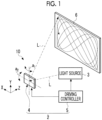
- the image drawing system 10 comprises an optical scanning device 2 and a light source 3.
- the optical scanning device 2 comprises a micromirror device (hereinafter, referred to as an "MMD") 4 and a driving controller 5.
- the driving controller 5 is an example of a processor according to the embodiment of the technique of the disclosure.
- the image drawing system 10 draws an image by optically scanning a surface to be scanned 6 by reflecting a light beam L of irradiation from the light source 3 using the MMD 4 under control of the driving controller 5.
- the surface to be scanned 6 is, for example, a screen for projecting the image, or a retina of an eye of a person.
- the image drawing system 10 is applied to, for example, a Lissajous scanning type laser display.
- the image drawing system 10 can be applied to a laser scanning display such as augmented reality (AR) glasses or virtual reality (VR) glasses.
- AR augmented reality
- VR virtual reality
- the MMD 4 is a piezoelectric biaxial drive type micromirror device capable of causing a mirror portion 20 (see Fig. 2 ) to swing around a first axis a 1 and around a second axis a 2 orthogonal to the first axis a 1 .
- a direction parallel to the second axis a 2 will be referred to as an X direction
- a direction parallel to the first axis a 1 will be referred to as a Y direction
- a direction orthogonal to the first axis a 1 and to the second axis a 2 will be referred to as a Z direction.
- first axis a 1 may intersect with the second axis a 2 at an angle other than 90°.
- intersecting means being within a constant angle range that is centered at 90 degrees and that includes a permissible error.
- the light source 3 is a laser device that emits, for example, laser light as the light beam L.
- the light source 3 outputs laser light of three colors of red (R), green (G), and blue (B).
- R red
- G green
- B blue
- the light source 3 perpendicularly irradiates a reflecting surface 20A (see Fig. 2 ) comprised in the mirror portion 20 with the light beam L in a state where the mirror portion 20 of the MMD 4 is at a standstill.
- the reflecting surface 20A is perpendicularly irradiated with the light beam L from the light source 3
- the light source 3 may be an obstacle in the drawing performed by scanning the surface to be scanned 6 with the light beam L.
- the reflecting surface 20A is perpendicularly irradiated with the light beam L emitted from the light source 3 by controlling the light beam L using an optical system such as a beam splitter.
- the optical system may include a lens or may not include a lens.
- an angle at which the reflecting surface 20A is irradiated with the light beam L emitted from the light source 3 is not limited to a perpendicular angle.
- the reflecting surface 20A may be irradiated with the light beam L in an inclined manner.
- the driving controller 5 outputs a driving signal to the light source 3 and to the MMD 4 based on optical scanning information.
- the light source 3 generates the light beam L based on the input driving signal and irradiates the MMD 4 with the light beam L.
- the MMD 4 causes the mirror portion 20 to swing around the first axis a 1 and the second axis a 2 based on the input driving signal.
- the mirror portion 20 By causing the mirror portion 20 to resonate around each of the first axis a 1 and the second axis a 2 via the driving controller 5, the light beam L reflected by the mirror portion 20 is scanned onto the surface to be scanned 6 such that the light beam L draws a Lissajous waveform.
- This optical scanning method is called a Lissajous scanning method.
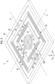
- the MMD 4 includes the mirror portion 20, a first support portion 21, a first movable frame 22, a second support portion 23, a second movable frame 24, a connecting portion 25, and a fixed frame 26.
- the MMD 4 is a so-called MEMS scanner.
- the mirror portion 20 has the reflecting surface 20A for reflecting an incidence ray.
- the reflecting surface 20A is provided on one surface of the mirror portion 20 and is formed with a thin metal film of, for example, gold (Au), aluminum (Al), silver (Ag), or a silver alloy.
- a shape of the reflecting surface 20A is, for example, a circular shape centered at an intersection between the first axis a 1 and the second axis a 2 .
- the first axis a 1 and the second axis a 2 are present in a plane including the reflecting surface 20A at a time of a standstill when the mirror portion 20 is at a standstill.
- a planar shape of the MMD 4 is a rectangular shape and is axially symmetric with respect to the first axis a 1 and axially symmetric with respect to the second axis a 2 .
- the first support portion 21 is arranged outside the mirror portion 20 at each of positions that face each other with the second axis a 2 interposed therebetween.
- the first support portions 21 are connected to the mirror portion 20 on the first axis a 1 and support the mirror portion 20 to be capable of swinging around the first axis a 1 .
- the first support portions 21 are torsion bars that stretch along the first axis a 1 .
- the first movable frame 22 is a frame having a rectangular shape surrounding the mirror portion 20 and is connected to the mirror portion 20 through the first support portion 21 on the first axis a 1 .
- a piezoelectric element 30 is formed on the first movable frame 22 at each of positions that face each other with the first axis a 1 interposed therebetween. In such a manner, a pair of first actuators 31 are configured by forming two piezoelectric elements 30 on the first movable frame 22.
- the pair of first actuators 31 are arranged at positions that face each other with the first axis a 1 interposed therebetween.
- the first actuators 31 cause the mirror portion 20 to swing around the first axis a 1 by applying rotational torque around the first axis a 1 to the mirror portion 20.
- the second support portion 23 is arranged outside the first movable frame 22 at each of positions that face each other with the first axis a 1 interposed therebetween.
- the second support portions 23 are connected to the first movable frame 22 on the second axis a 2 and support the first movable frame 22 and the mirror portion 20 to be capable of swinging around the second axis a 2 .
- the second support portions 23 are torsion bars that stretch along the second axis a 2 .
- the second movable frame 24 is a frame having a rectangular shape surrounding the first movable frame 22 and is connected to the first movable frame 22 through the second support portion 23 on the second axis a 2 .
- the piezoelectric element 30 is formed on the second movable frame 24 at each of positions that face each other with the second axis a 2 interposed therebetween. In such a manner, a pair of second actuators 32 are configured by forming two piezoelectric elements 30 on the second movable frame 24.
- the pair of second actuators 32 are arranged at positions that face each other with the second axis a 2 interposed therebetween.
- the second actuators 32 cause the mirror portion 20 to swing around the second axis a 2 by applying rotational torque about the second axis a 2 to the mirror portion 20 and to the first movable frame 22.
- the connecting portion 25 is arranged outside the second movable frame 24 at each of positions that face each other with the first axis a 1 interposed therebetween.
- the connecting portions 25 are connected to the second movable frame 24 on the second axis a 2 .
- the fixed frame 26 is a frame having a rectangular shape surrounding the second movable frame 24 and is connected to the second movable frame 24 through the connecting portion 25 on the second axis a 2 .
- a pair of first angle detection sensors 11A and 11B are provided in the first movable frame 22 near the first support portions 21 at positions that face each other with the first axis a 1 interposed therebetween.
- Each of the pair of first angle detection sensors 11A and 11B is configured with a piezoelectric element.
- Each of the first angle detection sensors 11A and 11B outputs a signal by converting a force applied by deformation of the first support portion 21 accompanied by rotational movement of the mirror portion 20 around the first axis a 1 into a voltage. That is, the first angle detection sensors 11A and 11B output signals corresponding to an angle of the mirror portion 20 around the first axis a 1 .
- a pair of second angle detection sensors 12A and 12B are provided in the second movable frame 24 near the second support portions 23 at positions that face each other with the second axis a 2 interposed therebetween.
- Each of the pair of second angle detection sensors 12A and 12B is configured with a piezoelectric element.
- Each of the second angle detection sensors 12A and 12B outputs a signal by converting a force applied by deformation of the second support portion 23 accompanied by rotational movement of the mirror portion 20 around the second axis a 2 into a voltage. That is, the second angle detection sensors 12A and 12B output signals corresponding to the angle of the mirror portion 20 around the second axis a 2 .
- wiring lines and electrode pads for providing driving signals to the first actuators 31 and the second actuators 32 are not shown.
- wiring lines and electrode pads for outputting signals from the first angle detection sensors 11A and 11B and from the second angle detection sensors 12A and 12B are not shown.
- a plurality of electrode pads are provided on the fixed frame 26.
- a deflection angle (hereinafter, referred to as a "first deflection angle”) ⁇ 1 of the mirror portion 20 around the first axis a 1 is controlled based on the driving signal (hereinafter, referred to as a "first driving signal") provided to the first actuators 31 by the driving controller 5.
- the first driving signal is, for example, a sinusoidal alternating current voltage.
- the first driving signal includes a driving voltage waveform V 1A (t) applied to one of the pair of first actuators 31 and a driving voltage waveform V 1B (t) applied to the other.
- the driving voltage waveform V 1A (t) and the driving voltage waveform V 1B (t) are in anti-phase with each other (that is, have a phase difference of 180°).
- the first deflection angle ⁇ 1 is an angle at which a line normal to the reflecting surface 20A is inclined with respect to the Z direction in an XZ plane.
- a deflection angle (hereinafter, referred to as a "second deflection angle”) ⁇ 2 of the mirror portion 20 around the second axis a 2 is controlled based on the driving signal (hereinafter, referred to as a "second driving signal") provided to the second actuators 32 by the driving controller 5.
- the second driving signal is, for example, a sinusoidal alternating current voltage.
- the second driving signal includes a driving voltage waveform V 2A (t) applied to one of the pair of second actuators 32 and a driving voltage waveform V 2B (t) applied to the other.
- the driving voltage waveform V 2A (t) and the driving voltage waveform V 2B (t) are in anti-phase with each other (that is, have a phase difference of 180°).
- the second deflection angle ⁇ 2 is an angle at which the line normal to the reflecting surface 20A is inclined with respect to the Z direction in a YZ plane.
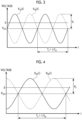
- Fig. 3 shows an example of the first driving signal
- Fig. 4 shows an example of the second driving signal
- Fig. 3 shows the driving voltage waveforms V 1A (t) and V 1B (t) included in the first driving signal
- Fig. 4 shows the driving voltage waveforms V 2A (t) and V 2B (t) included in the second driving signal.
- V 1A (t) and V 1B (t) are represented as follows.
- V 1 A t V off 1 + V 1 sin 2 ⁇ f d 1 t
- V 1 B t V off 1 + V 1 sin 2 ⁇ f d 1 t + ⁇
- Vi is an amplitude voltage.
- V off1 is a bias voltage.
- V off1 may be zero.
- fai is a driving frequency (hereinafter, referred to as a "first driving frequency").
- t is time.
- the mirror portion 20 swings around the first axis a 1 with the first driving frequency fai.
- V 2A (t) and V 2B (t) are represented as follows.
- V 2 A t V off 2 + V 2 sin 2 ⁇ f d 2 t + ⁇
- V 2 B t V off 2 + V 2 sin 2 ⁇ f d 2 t + ⁇ + ⁇
- V 2 is an amplitude voltage.
- V off2 is a bias voltage.
- V off2 may be zero.
- f d2 is a driving frequency (hereinafter, referred to as a "second driving frequency").
- t is time.
- ⁇ is a phase difference between the driving voltage waveforms V 1A (t) and V 1B (t) and the driving voltage waveforms V 2A (t) and V 2B (t).
- the mirror portion 20 swings around the second axis a 2 with the second driving frequency f d2 .
- the first driving frequency fai is set to match a resonance frequency of the mirror portion 20 around the first axis a 1 .
- the second driving frequency f d2 is set based on the first driving frequency fai and on a frequency ratio H between the first driving frequency fai and the second driving frequency f d2 .
- the frequency ratio H is set based on scanning density of light corresponding to a drawing pattern.
- the MMD 4 is set such that the second driving frequency f d2 matches a resonance frequency of the mirror portion 20 around the second axis a 2 .
- f d1 > f d2 is assumed.
- the mirror portion 20 has a higher swing frequency around the first axis a 1 than a swing frequency around the second axis a 2 .
- the first driving frequency fai and the second driving frequency f d2 may not necessarily match the resonance frequency.
- each of the first driving frequency fai and the second driving frequency f d2 may be a frequency within a frequency range near the resonance frequency (for example, a half-width range of a frequency distribution having the resonance frequency as a peak value).
- this frequency range is within a range of a so-called Q-value.
- the driving controller 5 includes a first driving signal generation portion 60A, a second driving signal generation portion 60B, a first signal processing portion 61A, a second signal processing portion 61B, a first phase shift portion 62A, a second phase shift portion 62B, a first derivation portion 63A, a second derivation portion 63B, a first zero cross pulse output portion 65A, a second zero cross pulse output portion 65B, and a light source driving portion 66.
- the first driving signal generation portion 60A, the first signal processing portion 61A, and the first phase shift portion 62A may perform a feedback control to maintain a vibration state where the swing of the mirror portion 20 around the first axis a 1 has a designated frequency.
- the second driving signal generation portion 60B, the second signal processing portion 61B, and the second phase shift portion 62B may perform a feedback control to maintain a vibration state where the swing of the mirror portion 20 around the second axis a 2 has a designated frequency.
- the first driving signal generation portion 60A generates the first driving signal including the driving voltage waveforms V 1A (t) and V 1B (t) based on a reference waveform and provides the generated first driving signal to the pair of first actuators 31 through the first phase shift portion 62A. Accordingly, the mirror portion 20 swings around the first axis a 1 .
- the second driving signal generation portion 60B generates the second driving signal including the driving voltage waveforms V 2A (t) and V 2B (t) based on the reference waveform and provides the generated second driving signal to the pair of second actuators 32 through the second phase shift portion 62B. Accordingly, the mirror portion 20 swings around the second axis a 2 .
- the first driving signal generated by the first driving signal generation portion 60A and the second driving signal generated by the second driving signal generation portion 60B are synchronized in phase as shown by ⁇ in the expressions showing the driving voltage waveforms V 2A (t) and V 2B (t) included in the second driving signal.
- the first angle detection sensors 11A and 11B output the signals corresponding to the angle of the mirror portion 20 around the first axis a 1 .
- the second angle detection sensors 12A and 12B output the signals corresponding to the angle of the mirror portion 20 around the second axis a 2 .
- Fig. 6 shows an example of the signals output from the pair of first angle detection sensors 11A and 11B.
- S1a 1 and S1a 2 represent the signals output from the pair of first angle detection sensors 11A and 11B in a case where the mirror portion 20 is caused to swing around only the first axis a 1 and to not swing around the second axis a 2 .
- the signals S1a 1 and S1a 2 are waveform signals similar to a sinusoidal wave having the first driving frequency fai and are in anti-phase with each other.
- a vibration noise RN1 caused by the swing of the mirror portion 20 around the second axis a 2 is superimposed on the output signals of the pair of first angle detection sensors 11A and 11B.
- S1b 1 represents a signal after the vibration noise RN1 is superimposed on the signal S1a 1 .
- S1b 2 represents a signal after the vibration noise RN1 is superimposed on the signal S1a 2 .
- the vibration noise RN1 is shown in a highlighted manner for description of the present embodiment.
- Fig. 7 shows an example of the signals output from the pair of second angle detection sensors 12A and 12B.
- S2a 1 and S2a 2 represent the signals output from the pair of second angle detection sensors 12A and 12B in a case where the mirror portion 20 is caused to swing around only the second axis a 2 and to not swing around the first axis a 1 .
- the signals S2a 1 and S2a 2 are waveform signals similar to a sinusoidal wave having the second driving frequency f d2 and are in anti-phase with each other.
- a vibration noise RN2 caused by the swing of the mirror portion 20 around the first axis a 1 is superimposed on the output signals of the pair of second angle detection sensors 12A and 12B.
- S2b 1 represents a signal obtained by the superimposition of the vibration noise RN2 on the signal S2a 1 .
- S2b 2 represents a signal obtained by the superimposition of the vibration noise RN2 on the signal S2a 2 .
- the vibration noise RN2 is shown in a highlighted manner for description of the present embodiment.
- the first signal processing portion 61A generates a signal (hereinafter, referred to as a "first angle detection signal”) S1c obtained by removing the vibration noise RN1 based on S1a 1 and S1a 2 output from the pair of first angle detection sensors 11A and 11B.
- the second signal processing portion 61B generates a signal (hereinafter, referred to as a "second angle detection signal”) S2c obtained by removing the vibration noise RN2 based on S2a 1 and S2a 2 output from the pair of second angle detection sensors 12A and 12B.
- the first signal processing portion 61A can be implemented by, for example, a circuit having a configuration shown in Fig. 8 as an example. As shown in Fig. 8 , the first signal processing portion 61A is configured with a buffer amplifier 71, a variable gain amplifier 72, a subtraction circuit 73, and a gain adjustment circuit 74.
- the gain adjustment circuit 74 is configured with a first band pass filter (BPF) circuit 75A, a second BPF circuit 75B, a first wave detection circuit 76A, a second wave detection circuit 76B, and a subtraction circuit 77.
- BPF band pass filter
- the subtraction circuit 73 and the subtraction circuit 77 are differential amplification circuits configured with operational amplifiers.
- the signal S1b 1 output from the first angle detection sensor 11A is input into a positive input terminal (non-inverting input terminal) of the subtraction circuit 73 through the buffer amplifier 71.
- a signal output from the buffer amplifier 71 branches in the middle of being input into the subtraction circuit 73 and is input into the first BPF circuit 75A in the gain adjustment circuit 74.
- the signal S1b 2 output from the first angle detection sensor 11B is input into a negative input terminal (inverting input terminal) of the subtraction circuit 73 through the variable gain amplifier 72.
- a signal output from the variable gain amplifier 72 branches in the middle of being input into the subtraction circuit 73 and is input into the second BPF circuit 75B in the gain adjustment circuit 74.
- Each of the first BPF circuit 75A and the second BPF circuit 75B has a passband B1 having the second driving frequency f d2 as a center frequency.
- the passband B1 is a frequency band of f d2 ⁇ 5 kH.
- the vibration noise RN1 has the second driving frequency f d2 and thus, passes through the passband B1. Accordingly, the first BPF circuit 75A extracts the vibration noise RN1 from the signal input from the buffer amplifier 71 and outputs the vibration noise RN1.
- the second BPF circuit 75B extracts the vibration noise RN1 from the signal input from the variable gain amplifier 72 and outputs the vibration noise RN1.
- Each of the first wave detection circuit 76A and the second wave detection circuit 76B is configured with, for example, a root mean squared value to direct current converter (RMS-DC converter).
- the first wave detection circuit 76A converts an amplitude of the vibration noise RN1 input from the first BPF circuit 75A into a DC voltage signal and inputs the DC voltage signal into a positive input terminal of the subtraction circuit 77.
- the second wave detection circuit 76B converts the amplitude of the vibration noise RN1 input from the second BPF circuit 75B into a DC voltage signal and inputs the DC voltage signal into a negative input terminal of the subtraction circuit 77.
- the subtraction circuit 77 outputs a value d 1 obtained by subtracting the DC voltage signal input from the second wave detection circuit 76B, from the DC voltage signal input from the first wave detection circuit 76A.
- the value d 1 corresponds to a difference between the amplitude of the vibration noise RN1 included in the signal S1b 1 output from the first angle detection sensor 11A and the amplitude of the vibration noise RN1 included in the signal S1b 2 output from the first angle detection sensor 11B.
- the subtraction circuit 77 inputs the value d 1 into a gain adjustment terminal of the variable gain amplifier 72 as a gain adjustment value.
- the variable gain amplifier 72 adjusts an amplitude level of the signal S1b 2 by multiplying the signal S1b 2 input from the first angle detection sensor 11B by the value d 1 input as the gain adjustment value. In such a manner, by performing a feedback control via the gain adjustment circuit 74, the amplitude of the vibration noise RN1 included in the signal S1b 2 after passing through the variable gain amplifier 72 is adjusted to match the amplitude of the vibration noise RN1 included in the signal S1b 1 after passing through the buffer amplifier 71.
- the subtraction circuit 73 outputs a value obtained by subtracting the signal S1b 2 input into the negative input terminal from the signal S1b 1 input into the positive input terminal. Since the amplitudes of the vibration noises RN1 included in both signals are matched by the feedback control, the vibration noises RN1 included in both signals are offset by subtraction processing performed by the subtraction circuit 73. Accordingly, the first angle detection signal S1c (see Fig. 9 ) that is a signal obtained by removing the vibration noise RN1 is output from the subtraction circuit 73.
- Fig. 9 shows a state where the first angle detection signal S1c is generated based on S1b 1 and S1b 2 output from the pair of first angle detection sensors 11A and 11B.
- the first angle detection signal S1c corresponds to a signal obtained by doubling an amplitude of the signal obtained by removing the vibration noise RN1 from the signal S1b 1 .
- the first angle detection signal S1c output from the first signal processing portion 61A has a delay of 90° in phase with respect to the driving voltage waveform V 1A (t) included in the first driving signal as shown in Fig. 9 .
- the second signal processing portion 61B can be implemented by the same configuration as the first signal processing portion 61A and thus, will not be described.
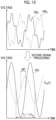
- Fig. 10 shows a state where the second angle detection signal S2c is generated based on S2b 1 and S2b 2 output from the pair of second angle detection sensors 12A and 12B.
- the second angle detection signal S2c corresponds to a signal obtained by doubling an amplitude of the signal obtained by removing the vibration noise RN2 from the signal S2bi.
- the second angle detection signal S2c output from the second signal processing portion 61B has a delay of 90° in phase with respect to the driving voltage waveform V 2A (t) included in the second driving signal as shown in Fig. 10 .
- the first angle detection signal S1c generated by the first signal processing portion 61A is fed back to the first driving signal generation portion 60A.
- the first phase shift portion 62A shifts phases of the driving voltage waveforms output from the first driving signal generation portion 60A. For example, the first phase shift portion 62A shifts the phases by 90°.
- the second angle detection signal S2c generated by the second signal processing portion 61B is fed back to the second driving signal generation portion 60B.
- the second phase shift portion 62B shifts phases of the driving voltage waveforms output from the second driving signal generation portion 60B. For example, the second phase shift portion 62B shifts the phases by 90°.
- the first angle detection signal S1c generated by the first signal processing portion 61A is ideally a sinusoidal wave but is generally not a smooth sinusoidal wave. This is because an effect of the swing of the mirror portion 20 around the second axis a 2 cannot be removed in processing performed by the first signal processing portion 61A.
- the second angle detection signal S2c generated by the second signal processing portion 61B is also ideally a sinusoidal wave but is generally not a smooth sinusoidal wave because an effect of the swing of the mirror portion 20 around the first axis a 1 remains.
- a timing at which the second angle detection signal S2c crosses zero is slightly shifted from a timing at which the second deflection angle ⁇ 2 actually becomes equal to 0°.
- a dot dashed line shows an ideal sinusoidal waveform representing the swing of the mirror portion 20 around the second axis a 2
- a double dot dashed line shows a waveform of the effect of the swing of the mirror portion 20 around the first axis a 1 .
- a solid line represents the second angle detection signal S2c. While the second angle detection signal S2c is illustratively described in Fig. 11 , the effect of the swing of the mirror portion 20 around the second axis a 2 is also included in the first angle detection signal S1c.
- the present applicant has found that shifting of a first timing at which the second angle detection signal S2c crosses zero to before and to after a second timing at which the second deflection angle ⁇ 2 actually becomes equal to 0° is repeated. Furthermore, the present applicant has found that within a period of time of one frame of a motion image to be drawn, a total value of a shift amount in a case where the first timing is shifted to before the second timing is approximately equal to a total value of a shift amount in a case where the first timing is shifted to after the second timing.
- the first derivation portion 63A reduces the effect of the swing of the mirror portion 20 around the second axis a 2 by integrating a phase delay time (hereinafter, referred to as a "first phase delay time”) of the first angle detection signal S1c with respect to the first driving signal within the period of time of one frame.
- the second derivation portion 63B reduces the effect of the swing of the mirror portion 20 around the first axis a 1 by integrating a phase delay time (hereinafter, referred to as a "second phase delay time”) of the second angle detection signal S2c with respect to the second driving signal within the period of time of one frame.
- the first driving signal is an example of a first signal to be referred to according to the embodiment of the technique of the disclosure
- the second driving signal is an example of a second signal to be referred to according to the embodiment of the technique of the disclosure.
- f out is the output frequency of the DDS.
- f c is a system clock frequency.
- N is a length of a phase accumulator.
- M is a tuning word value.
- the first driving frequency fai as a target is set to match the resonance frequency of the mirror portion 20 around the first axis a 1 .
- the second driving frequency f d2 as a target is calculated based on the first driving frequency fai and on the frequency ratio H between the first driving frequency fai and the second driving frequency f d2 .
- the frequency ratio H is set based on the scanning density of the light corresponding to the drawing pattern.
- the system clock frequency and the length of the phase accumulator are known.
- a tuning word value M1 with which the first driving frequency fai is obtained can be calculated using Expression (1).
- a tuning word value M2 with which the second driving frequency f d2 is obtained can be calculated using Expression (1).
- G a greatest common divisor of the tuning word value M1 and the tuning word value M2 is denoted by G.
- Q1 is a quotient obtained by dividing the tuning word value M1 by the greatest common divisor G.
- Q2 is a quotient obtained by dividing the tuning word value M2 by the greatest common divisor G.
- a period of time corresponding to a Q2 period of the first driving signal having the first driving frequency fai is equal to a period of time corresponding to a Q1 period of the second driving signal having the second driving frequency f d2 .
- this period of time is set as the period of time of one frame.
- the first derivation portion 63A derives a first integrated value by integrating the first phase delay time of the first angle detection signal S1c with respect to the first driving signal, the number of times that is n times the number of times corresponding to the period of time of one frame of the motion image to be drawn.
- n may be greater than or equal to 2.
- the first derivation portion 63A binarizes the first driving signal and the first angle detection signal S1c.
- the first derivation portion 63A binarizes the first driving signal and the first angle detection signal S1c by setting a value greater than or equal to an average value of a minimum value and a maximum value to 1 and by setting a value less than the average value to 0 for each of the first driving signal and the first angle detection signal S1c.
- the first derivation portion 63A derives the first integrated value by consecutively integrating the first phase delay time of the first angle detection signal S1c with respect to the first driving signal after binarization, the number of times corresponding to the period of time of one frame of the motion image to be drawn.
- the number of times of integration in this case is Q2 described above.
- the first phase delay time of a corresponding period is represented by C i (i is an integer of 0 to Q2 - 1).
- a difference in timing of a rising edge between the first driving signal and the first angle detection signal S1c after binarization is used in the example in Fig. 13
- a difference in timing of a falling edge between the first driving signal and the first angle detection signal S1c after binarization may also be used.
- the first derivation portion 63A derives a first average phase delay time that is an average value of the first phase delay time, by dividing the first integrated value by the number of times of integration.
- the second derivation portion 63B derives a second integrated value by integrating the second phase delay time of the second angle detection signal S2c with respect to the second driving signal, the number of times that is n times the number of times corresponding to the period of time of one frame of the motion image to be drawn.
- the second derivation portion 63B binarizes the second driving signal and the second angle detection signal S2c.
- the second derivation portion 63B binarizes the second driving signal and the second angle detection signal S2c by setting a value greater than or equal to an average value of a minimum value and a maximum value to 1 and by setting a value less than the average value to 0 for each of the second driving signal and the second angle detection signal S2c.
- the second derivation portion 63B derives the second integrated value by consecutively integrating the second phase delay time of the second angle detection signal S2c with respect to the second driving signal after binarization, the number of times corresponding to the period of time of one frame of the motion image to be drawn.
- the number of times of integration in this case is Q1 described above.
- the second phase delay time of a corresponding period is represented by C j (j is an integer of 0 to Q1 - 1).
- a difference in timing of a rising edge between the second driving signal and the second angle detection signal S2c after binarization is used in the example in Fig. 14
- a difference in timing of a falling edge between the second driving signal and the second angle detection signal S2c after binarization may also be used.
- the second derivation portion 63B derives a second average phase delay time that is an average value of the second phase delay time, by dividing the second integrated value by the number of times of integration.
- the first zero cross pulse output portion 65A generates a reference signal (hereinafter, referred to as a "first reference signal”) based on the first driving signal and on the first average phase delay time derived by the first derivation portion 63A.
- the first reference signal is a signal representing that the angle of the mirror portion 20 around the first axis a 1 is equal to a reference angle (hereinafter, referred to as a "first reference angle").
- first reference angle a reference angle
- the first zero cross pulse output portion 65A generates a zero cross pulse (hereinafter, referred to as a "first zero cross pulse") ZC1 as an example of the first reference signal based on the first driving signal and the first average phase delay time derived by the first derivation portion 63A.
- the first zero cross pulse output portion 65A is configured with a zero cross detection circuit.
- the first zero cross pulse is a zero cross signal representing that the angle of the mirror portion 20 around the first axis a 1 is zero.
- the first zero cross pulse output portion 65A generates the first zero cross pulse ZC1 at a point in time when the first average phase delay time elapses from a point in time when the first driving signal represents that the angle of the mirror portion 20 around the first axis a 1 is equal to the first reference angle (in the present embodiment, a point in time at which V off1 is crossed).
- the first zero cross pulse output portion 65A outputs the generated first zero cross pulse ZC1 to the light source driving portion 66.
- the second zero cross pulse output portion 65B generates a reference signal (hereinafter, referred to as a "second reference signal") based on the second driving signal and on the second average phase delay time derived by the second derivation portion 63B.
- the second reference signal is a signal representing that the angle of the mirror portion 20 around the second axis a 2 is equal to a reference angle (hereinafter, referred to as a "second reference angle").
- a reference angle hereinafter, referred to as a "second reference angle"
- the second zero cross pulse output portion 65B generates a zero cross pulse (hereinafter, referred to as a "second zero cross pulse") ZC2 as an example of the second reference signal based on the second driving signal and the second average phase delay time derived by the second derivation portion 63B.
- the second zero cross pulse output portion 65B is configured with a zero cross detection circuit.
- the second zero cross pulse is a zero cross signal representing that the angle of the mirror portion 20 around the second axis a 2 is zero.
- the second zero cross pulse output portion 65B generates the second zero cross pulse ZC2 at a point in time when the second average phase delay time elapses from a point in time when the second driving signal represents that the angle of the mirror portion 20 around the second axis a 2 is equal to the second reference angle (in the present embodiment, a point in time at which V off2 is crossed).
- the second zero cross pulse output portion 65B outputs the generated second zero cross pulse ZC2 to the light source driving portion 66.
- first zero cross pulse output portion 65A and the second zero cross pulse output portion 65B output the zero cross pulses using both of the point in time when the sinusoidal wave becomes zero from a negative value toward a positive value and the point in time when the sinusoidal wave becomes zero from a positive value toward a negative value
- the present disclosure is not limited thereto.
- the first zero cross pulse output portion 65A and the second zero cross pulse output portion 65B may output the zero cross pulses using any one of the point in time when the sinusoidal wave becomes zero from a negative value toward a positive value or the point in time when the sinusoidal wave becomes zero from a positive value toward a negative value.
- the light source driving portion 66 drives the light source 3 based on, for example, drawing data supplied from an outside of the image drawing system 10.
- the light source driving portion 66 controls an irradiation timing of the laser light by the light source 3 so that the irradiation timing is synchronized with the first zero cross pulse ZC1 and with the second zero cross pulse ZC2.
- the first average phase delay time derivation processing is executed at a predetermined time interval during the drawing of the image performed by the image drawing system 10.
- the time interval may be a time interval corresponding to the period of time of one frame or may be a time interval corresponding to a period of time of a plurality of frames.
- step S10 in Fig. 17 the first derivation portion 63A binarizes the first driving signal and the first angle detection signal S1c as described above.
- step S12 the first derivation portion 63A derives the first integrated value by consecutively integrating the first phase delay time of the first angle detection signal S1c with respect to the first driving signal after binarization performed by the processing in step S10, the number of times corresponding to the period of time of one frame of the motion image to be drawn.
- step S14 the first derivation portion 63A derives the first average phase delay time that is the average value of the first phase delay time, by dividing the first integrated value derived in step S12 by the number of times of integration. In a case where the processing in step S14 ends, the first average phase delay time derivation processing ends.
- the first average phase delay time is updated by periodically executing the first average phase delay time derivation processing during the drawing of the image.
- the second average phase delay time derivation processing is executed at a predetermined time interval during the drawing of the image performed by the image drawing system 10.
- the time interval may be a time interval corresponding to the period of time of one frame or may be a time interval corresponding to a period of time of a plurality of frames.
- the second average phase delay time derivation processing may be executed at the same time as the first average phase delay time derivation processing.
- step S20 in Fig. 18 the second derivation portion 63B binarizes the second driving signal and the second angle detection signal S2c as described above.
- step S22 the second derivation portion 63B derives the second integrated value by consecutively integrating the second phase delay time of the second angle detection signal S2c with respect to the second driving signal after binarization performed by the processing in step S20, the number of times corresponding to the period of time of one frame of the motion image to be drawn.
- step S24 the second derivation portion 63B derives the second average phase delay time that is the average value of the second phase delay time, by dividing the second integrated value derived in step S22 by the number of times of integration as described above. In a case where the processing in step S24 ends, the second average phase delay time derivation processing ends.
- the second average phase delay time is updated by periodically executing the second average phase delay time derivation processing during the drawing of the image.
- first zero cross pulse generation processing is executed during the drawing of the image performed by the image drawing system 10.
- the first zero cross pulse output portion 65A generates a binarized signal of the first driving signal generated by the first driving signal generation portion 60A.
- a method for binarization may be a method of using a comparator or may be a method of providing a register of 1 bit in a field programmable gate array (FPGA).
- the first zero cross pulse output portion 65A outputs a binarization signal obtained by delaying the binarized signal by the first average phase delay time, to the light source driving portion 66 as the first zero cross pulse ZC1, and the first zero cross pulse generation processing ends.
- the second zero cross pulse generation processing is executed during the drawing of the image performed by the image drawing system 10.
- the second zero cross pulse output portion 65B generates a binarized signal of the second driving signal generated by the second driving signal generation portion 60B.
- a method for binarization may be a method of using a comparator or a method of providing a register of 1 bit in an FPGA.
- the second zero cross pulse output portion 65B outputs a binarization signal obtained by delaying the binarized signal by the second average phase delay time, to the light source driving portion 66 as the second zero cross pulse ZC2, and the second zero cross pulse generation processing ends.
- Fig. 19 illustrates an example of a relationship between a standard deviation of the first integrated value derived a constant number of times (for example, 1000 times) and the number of times of integration.
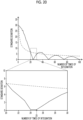
- Fig. 20 illustrates an example of a relationship between a standard deviation of the second integrated value derived the constant number of times and the number of times of integration.
- the standard deviation of the first integrated value is decreased, that is, as variations in the first integrated value are decreased, the effect of the swing of the mirror portion 20 around the second axis a 2 can be removed more from the first angle detection signal S1c.
- the standard deviation of the second integrated value is decreased, that is, as variations in the second integrated value are decreased, the effect of the swing of the mirror portion 20 around the first axis a 1 can be removed more from the second angle detection signal S2c.
- FIG. 19 shows the standard deviation of the first integrated value in a case where processing of deriving the first integrated value while changing the number of times of integration from 1 to 100 is performed the constant number of times.
- a lower part of Fig. 19 is an enlarged part (a part surrounded by a rectangle of a broken line) in which the number of times of integration is 40 to 60 in the upper part of Fig. 19 .
- a solid line in Fig. 19 represents the standard deviation of the first integrated value in a case where the first phase delay time is consecutively integrated as in the embodiment.
- a dot dashed line in Fig. 19 represents the standard deviation of the first integrated value in a case where the first phase delay time is randomly selected and integrated as a comparative example.
- FIG. 20 shows the standard deviation of the second integrated value in a case where processing of deriving the second integrated value while changing the number of times of integration from 1 to 100 is performed the constant number of times.
- a lower part of Fig. 20 is an enlarged part (a part surrounded by a rectangle of a broken line) in which the number of times of integration is 20 to 30 in the upper part of Fig. 20 .
- a solid line in Fig. 20 represents the standard deviation of the second integrated value in a case where the second phase delay time is consecutively integrated as in the embodiment.
- a dot dashed line in Fig. 20 represents the standard deviation of the second integrated value in a case where the second phase delay time is randomly selected and integrated as a comparative example.
- Fig. 19 and Fig. 20 show results in a case where the first phase delay time and the second phase delay time are represented by the number of clocks of a system clock.
- Fig. 19 and Fig. 20 show results in a case where the optical scanning device 2 is driven by setting Q1 to 25 and by setting Q2 to 51.
- a degree of decrease in the standard deviation of the first integrated value is decreased in a case where the number of times of integration becomes greater than or equal to a certain number. That is, in the comparative example, the number of times of integration is to be increased in order to decrease the standard deviation of the first integrated value.
- the standard deviation of the first integrated value tends to be decreased as the number of times of integration is increased.
- the standard deviation of the first integrated value is the smallest in a case where the number of times of integration is Q2 (here, 51).
- a case where the number of times of integration is Q2 is a case where the number of times of integration is the number of times corresponding to the period of time of one frame of the motion image to be drawn.
- a degree of decrease in the standard deviation of the second integrated value is decreased in a case where the number of times of integration becomes greater than or equal to a certain number. That is, in the comparative example, the number of times of integration is to be increased in order to decrease the standard deviation of the second integrated value.
- the standard deviation of the second integrated value tends to be decreased as the number of times of integration is increased.
- the standard deviation of the second integrated value is the smallest in a case where the number of times of integration is Q1 (here, 25).
- a case where the number of times of integration is Q1 is a case where the number of times of integration is the number of times corresponding to the period of time of one frame of the motion image to be drawn.
- the standard deviation of the second integrated value is also the smallest in a case where the number of times of integration is twice (here, 50), three times (here, 75), and four times (here, 100) greater than Q1.
- the first integrated value is derived by integrating the first phase delay time the number of times corresponding to the period of time of one frame of the motion image to be drawn.
- the first integrated value is obtained by reducing the effect of the swing of the mirror portion 20 around the second axis a 2 from the first angle detection signal S1c.
- the second integrated value is derived by integrating the second phase delay time the number of times corresponding to the period of time of one frame of the motion image to be drawn.
- the second integrated value is obtained by reducing the effect of the swing of the mirror portion 20 around the first axis a 1 from the second angle detection signal S2c.
- the number of times of integration in deriving the first integrated value and the second integrated value can be a small number.
- the first derivation portion 63A may derive the first integrated value by integrating the first phase delay time of the first angle detection signal S1c with respect to the first signal to be referred to that is a signal for reference corresponding to the first driving signal, such as a duplicated signal of the first driving signal.
- the second derivation portion 63B may derive the second integrated value by integrating the second phase delay time of the second angle detection signal S2c with respect to the second signal to be referred to that is a signal for reference corresponding to the second driving signal, such as a duplicated signal of the second driving signal.
- the configuration of the MMD 4 shown in the embodiment is an example.
- the configuration of the MMD 4 can be variously modified.
- the first actuators 31 that cause the mirror portion 20 to swing around the first axis a 1 may be arranged in the second movable frame 24, and the second actuators 32 that cause the mirror portion 20 to swing around the second axis a 2 may be arranged in the first movable frame 22.
- the pair of first angle detection sensors 11A and 11B are arranged at positions that face each other with the first axis a 1 interposed therebetween is described, the present disclosure is not limited thereto.
- the pair of first angle detection sensors 11A and 11B may be arranged at positions that face each other with the second axis a 2 interposed therebetween.
- each of the pair of first angle detection sensors 11A and 11B is arranged near the first support portions 21 on the first movable frame 22.
- the first angle detection sensor 11A is arranged near the first support portion 21 connected to one side of the mirror portion 20.
- the first angle detection sensor 11B is arranged near the first support portion 21 connected to the other side of the mirror portion 20. Accordingly, the pair of first angle detection sensors 11A and 11B are arranged at positions that face each other with the second axis a 2 interposed therebetween and that face each other with the mirror portion 20 interposed therebetween. In addition, the pair of first angle detection sensors 11A and 11B are arranged at positions that are shifted in the same direction (in the example in Fig. 21 , the -X direction) from the first axis a 1 .
- the vibration noise can be removed by subtracting one of the output signals of both of the first angle detection sensors 11A and 11B from the other.
- the vibration noise can be removed by adding the output signals of both of the first angle detection sensors 11A and 11B.
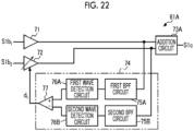
- the first signal processing portion 61A includes an addition circuit 73A instead of the subtraction circuit 73.
- the addition circuit 73A outputs a value obtained by adding the signal S1b 1 input from the first angle detection sensor 11A through the buffer amplifier 71 to the signal S1b 2 input from the first angle detection sensor 11B through the variable gain amplifier 72.
- the pair of second angle detection sensors 12A and 12B may be arranged at positions that face each other with the second axis a 1 interposed therebetween.
- the pair of second angle detection sensors 12A and 12B may be arranged near the second support portions 23 on the second movable frame 24.
- the second angle detection sensor 12A is arranged near the second support portion 23 connected to one side of the first movable frame 22.
- the second angle detection sensor 12B is arranged near the second support portion 23 connected to the other side of the first movable frame 22. Accordingly, the pair of second angle detection sensors 12A and 12B are arranged at positions that face each other with the first axis a 1 interposed therebetween and that face each other with the mirror portion 20 and the first movable frame 22 interposed therebetween. In addition, the pair of second angle detection sensors 12A and 12B are arranged at positions that are shifted in the same direction (in the example in Fig. 21 , the +Y direction) from the second axis a 2 .
- the vibration noise can be removed by subtracting one of the output signals of both of the second angle detection sensors 12A and 12B from the other.
- the vibration noise can be removed by adding the output signals of both of the second angle detection sensors 12A and 12B.
- a configuration of the second signal processing portion 61B in this form example can be implemented by the same configuration as the first signal processing portion 61A shown in Fig. 22 and thus, will not be described.
- a form of providing any one of the pair of first angle detection sensors 11A and 11B in the MMD 4 may be applied.
- a form of providing any one of the pair of second angle detection sensors 12A and 12B in the MMD 4 may be applied.
- the driving controller 5 can be configured using at least one of an analog operation circuit or a digital operation circuit.
- the driving controller 5 may be configured with one processor or may be configured with a combination of two or more processors of the same type or different types.
- Examples of the processor include a central processing unit (CPU), a programmable logic device (PLD), and a dedicated electric circuit.
- the CPU is a general-purpose processor that executes software (program) to function as various processing portions.
- the PLD is a processor such as an FPGA that has a circuit configuration changeable after manufacture.
- the dedicated electric circuit is a processor such as an application specific integrated circuit (ASIC) that has a circuit configuration dedicatedly designed to perform specific processing.
- ASIC application specific integrated circuit
Landscapes
- Physics & Mathematics (AREA)
- General Physics & Mathematics (AREA)
- Optics & Photonics (AREA)
- Mechanical Optical Scanning Systems (AREA)
- Mechanical Light Control Or Optical Switches (AREA)
Abstract
Description
- The present disclosure relates to an optical scanning device, a driving method of an optical scanning device, and an image drawing system.
- A micromirror device (also referred to as a microscanner) has been known as one of micro electro mechanical systems (MEMS) devices manufactured using the silicon (Si) nanofabrication technique. An optical scanning device comprising the micromirror device has a small size and low power consumption and thus, is expected to be applied to image drawing systems such as laser displays or laser projectors.
- In the micromirror device, a mirror portion is formed to be capable of swinging around a first axis and a second axis that are orthogonal to each other, and the swing of the mirror portion around each axis causes light reflected by the mirror portion to be two-dimensionally scanned. In addition, a micromirror device that can perform Lissajous scanning of light by causing a mirror portion to resonate around each axis has been known.
-
JP2016-184018A - An output signal of an angle detection sensor that detects an angle of the mirror portion around the first axis includes a noise and the like caused by the swing of the mirror portion around the second axis. Thus, detection accuracy of the angle of the mirror portion around the first axis may be decreased. Similarly, an output signal of an angle detection sensor that detects an angle of the mirror portion around the second axis includes a noise and the like caused by the swing of the mirror portion around the first axis. Thus, detection accuracy of the angle of the mirror portion around the second axis may be decreased.
- In the technique disclosed in
JP2016-184018A - The present disclosure is conceived in view of the above matter, and an object thereof is to provide an optical scanning device, a driving method of an optical scanning device, and an image drawing system that can suppress a decrease in detection accuracy of an angle of a mirror portion around a first axis and of an angle of the mirror portion around a second axis.
- An optical scanning device according to an aspect of the present disclosure is an optical scanning device comprising a mirror portion that has a reflecting surface on which an incidence ray is reflected, a first actuator that causes the mirror portion to swing around a first axis which is in a plane including the reflecting surface at a time of a standstill of the mirror portion, a second actuator that causes the mirror portion to swing around a second axis which is in the plane including the reflecting surface at the time of the standstill of the mirror portion and which intersects with the first axis, a first angle detection sensor that outputs a signal corresponding to an angle of the mirror portion around the first axis, a second angle detection sensor that outputs a signal corresponding to an angle of the mirror portion around the second axis, and at least one processor, in which the processor is configured to provide a first driving signal having a first driving frequency to the first actuator, provide a second driving signal having a second driving frequency to the second actuator, derive a first integrated value by integrating a first phase delay time of the output signal of the first angle detection sensor with respect to a first signal to be referred to corresponding to the first driving signal, the number of times that is greater by a factor of a natural number than the number of times corresponding to a period of time of one frame of a motion image to be drawn, and derive a second integrated value by integrating a second phase delay time of the output signal of the second angle detection sensor with respect to a second signal to be referred to corresponding to the second driving signal, the number of times that is greater by a factor of a natural number than the number of times corresponding to the period of time of one frame.
- In the optical scanning device according to the aspect of the present disclosure, the first signal to be referred to may be the first driving signal, and the second signal to be referred to may be the second driving signal.
- In addition, in the optical scanning device according to the aspect of the present disclosure, the processor may be configured to derive the first integrated value after binarizing the first driving signal and the output signal of the first angle detection sensor, and derive the second integrated value after binarizing the second driving signal and the output signal of the second angle detection sensor.
- In addition, in the optical scanning device according to the aspect of the present disclosure, the processor may be configured to derive a first average phase delay time that is an average value of the first phase delay time, by dividing the first integrated value by the number of times of integration, derive a second average phase delay time that is an average value of the second phase delay time, by dividing the second integrated value by the number of times of integration, output a first reference signal representing that the angle of the mirror portion around the first axis is equal to a first reference angle, at a point in time when the first average phase delay time elapses from a point in time when the first driving signal represents that the angle of the mirror portion around the first axis is equal to the first reference angle, and output a second reference signal representing that the angle of the mirror portion around the second axis is equal to a second reference angle, at a point in time when the second average phase delay time elapses from a point in time when the second driving signal represents that the angle of the mirror portion around the second axis is equal to the second reference angle.
- In addition, in the optical scanning device according to the aspect of the present disclosure, the first reference angle and the second reference angle may be zero.
- A driving method of an optical scanning device according to another aspect of the present disclosure is a driving method of an optical scanning device including a mirror portion that has a reflecting surface on which an incidence ray is reflected, a first actuator that causes the mirror portion to swing around a first axis which is in a plane including the reflecting surface at a time of a standstill of the mirror portion, a second actuator that causes the mirror portion to swing around a second axis which is in the plane including the reflecting surface at the time of the standstill of the mirror portion and which intersects with the first axis, a first angle detection sensor that outputs a signal corresponding to an angle of the mirror portion around the first axis, and a second angle detection sensor that outputs a signal corresponding to an angle of the mirror portion around the second axis, the driving method comprising providing a first driving signal having a first driving frequency to the first actuator, providing a second driving signal having a second driving frequency to the second actuator, deriving a first integrated value by integrating a first phase delay time of the output signal of the first angle detection sensor with respect to a first signal to be referred to corresponding to the first driving signal, the number of times that is greater by a factor of a natural number than the number of times corresponding to a period of time of one frame of a motion image to be drawn, and deriving a second integrated value by integrating a second phase delay time of the output signal of the second angle detection sensor with respect to a second signal to be referred to corresponding to the second driving signal, the number of times that is greater by a factor of a natural number than the number of times corresponding to the period of time of one frame.
- In addition, an image drawing system according to still another aspect of the present disclosure comprises above any optical scanning device, and a light source that irradiates the mirror portion with light.
- According to the present disclosure, a decrease in detection accuracy of the angle of the mirror portion around the first axis and of the angle of the mirror portion around the second axis can be suppressed.
-
-
Fig. 1 is a schematic diagram of an image drawing system. -
Fig. 2 is an external perspective view of a micromirror device. -
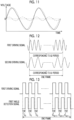
Fig. 3 is a graph showing an example of a first driving signal. -
Fig. 4 is a graph showing an example of a second driving signal. -
Fig. 5 is a block diagram showing an example of a functional configuration of a driving controller. -
Fig. 6 is a diagram showing an example of signals output from a pair of first angle detection sensors. -
Fig. 7 is a diagram showing an example of signals output from a pair of second angle detection sensors. -
Fig. 8 is a circuit diagram showing an example of a configuration of a first signal processing portion. -
Fig. 9 is a diagram showing an example of first signal processing. -
Fig. 10 is a diagram showing an example of second signal processing. -
Fig. 11 is a diagram for describing a shift in output signal of an angle detection sensor. -
Fig. 12 is a diagram for describing one frame. -
Fig. 13 is a diagram for describing derivation processing of a first integrated value. -
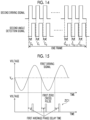
Fig. 14 is a diagram for describing derivation processing of a second integrated value. -
Fig. 15 is a diagram for describing generation processing of a first zero cross pulse. -
Fig. 16 is a diagram for describing generation processing of a second zero cross pulse. -
Fig. 17 is a flowchart showing an example of first average phase delay time derivation processing. -
Fig. 18 is a flowchart showing an example of second average phase delay time derivation processing. -
Fig. 19 is a graph showing an example of a relationship between a standard deviation of the first integrated value and the number of times of integration. -
Fig. 20 is a graph showing an example of a relationship between a standard deviation of the second integrated value and the number of times of integration. -
Fig. 21 is a plan view of a micromirror device according to a modification example. -
Fig. 22 is a circuit diagram showing a configuration of a first signal processing portion according to the modification example. - Hereinafter, an embodiment according to the technique of the present disclosure will be described in detail with reference to the drawings.
- First, a configuration of an
image drawing system 10 according to the present embodiment will be described with reference toFig. 1 . As shown inFig. 1 , theimage drawing system 10 comprises anoptical scanning device 2 and alight source 3. Theoptical scanning device 2 comprises a micromirror device (hereinafter, referred to as an "MMD") 4 and adriving controller 5. Thedriving controller 5 is an example of a processor according to the embodiment of the technique of the disclosure. - The
image drawing system 10 draws an image by optically scanning a surface to be scanned 6 by reflecting a light beam L of irradiation from thelight source 3 using theMMD 4 under control of thedriving controller 5. The surface to be scanned 6 is, for example, a screen for projecting the image, or a retina of an eye of a person. - The
image drawing system 10 is applied to, for example, a Lissajous scanning type laser display. Specifically, theimage drawing system 10 can be applied to a laser scanning display such as augmented reality (AR) glasses or virtual reality (VR) glasses. - The
MMD 4 is a piezoelectric biaxial drive type micromirror device capable of causing a mirror portion 20 (seeFig. 2 ) to swing around a first axis a1 and around a second axis a2 orthogonal to the first axis a1. Hereinafter, a direction parallel to the second axis a2 will be referred to as an X direction, a direction parallel to the first axis a1 will be referred to as a Y direction, and a direction orthogonal to the first axis a1 and to the second axis a2 will be referred to as a Z direction. In the present embodiment, while an example in which the first axis a1 is orthogonal to (that is, perpendicularly intersects with) the second axis a2 is shown, the first axis a1 may intersect with the second axis a2 at an angle other than 90°. Here, intersecting means being within a constant angle range that is centered at 90 degrees and that includes a permissible error. - The
light source 3 is a laser device that emits, for example, laser light as the light beam L. For example, thelight source 3 outputs laser light of three colors of red (R), green (G), and blue (B). It is preferable that thelight source 3 perpendicularly irradiates a reflectingsurface 20A (seeFig. 2 ) comprised in themirror portion 20 with the light beam L in a state where themirror portion 20 of theMMD 4 is at a standstill. In a case where the reflectingsurface 20A is perpendicularly irradiated with the light beam L from thelight source 3, thelight source 3 may be an obstacle in the drawing performed by scanning the surface to be scanned 6 with the light beam L. Thus, it is preferable that the reflectingsurface 20A is perpendicularly irradiated with the light beam L emitted from thelight source 3 by controlling the light beam L using an optical system such as a beam splitter. The optical system may include a lens or may not include a lens. In addition, an angle at which the reflectingsurface 20A is irradiated with the light beam L emitted from thelight source 3 is not limited to a perpendicular angle. The reflectingsurface 20A may be irradiated with the light beam L in an inclined manner. - The driving
controller 5 outputs a driving signal to thelight source 3 and to theMMD 4 based on optical scanning information. Thelight source 3 generates the light beam L based on the input driving signal and irradiates theMMD 4 with the light beam L. TheMMD 4 causes themirror portion 20 to swing around the first axis a1 and the second axis a2 based on the input driving signal. - By causing the
mirror portion 20 to resonate around each of the first axis a1 and the second axis a2 via the drivingcontroller 5, the light beam L reflected by themirror portion 20 is scanned onto the surface to be scanned 6 such that the light beam L draws a Lissajous waveform. This optical scanning method is called a Lissajous scanning method. - Next, a configuration of the
MMD 4 according to the present embodiment will be described with reference toFig. 2 . As shown inFig. 2 , theMMD 4 includes themirror portion 20, afirst support portion 21, a firstmovable frame 22, asecond support portion 23, a secondmovable frame 24, a connectingportion 25, and a fixedframe 26. TheMMD 4 is a so-called MEMS scanner. - The
mirror portion 20 has the reflectingsurface 20A for reflecting an incidence ray. The reflectingsurface 20A is provided on one surface of themirror portion 20 and is formed with a thin metal film of, for example, gold (Au), aluminum (Al), silver (Ag), or a silver alloy. A shape of the reflectingsurface 20A is, for example, a circular shape centered at an intersection between the first axis a1 and the second axis a2. - The first axis a1 and the second axis a2 are present in a plane including the reflecting
surface 20A at a time of a standstill when themirror portion 20 is at a standstill. A planar shape of theMMD 4 is a rectangular shape and is axially symmetric with respect to the first axis a1 and axially symmetric with respect to the second axis a2. - The
first support portion 21 is arranged outside themirror portion 20 at each of positions that face each other with the second axis a2 interposed therebetween. Thefirst support portions 21 are connected to themirror portion 20 on the first axis a1 and support themirror portion 20 to be capable of swinging around the first axis a1. In the present embodiment, thefirst support portions 21 are torsion bars that stretch along the first axis a1. - The first
movable frame 22 is a frame having a rectangular shape surrounding themirror portion 20 and is connected to themirror portion 20 through thefirst support portion 21 on the first axis a1. Apiezoelectric element 30 is formed on the firstmovable frame 22 at each of positions that face each other with the first axis a1 interposed therebetween. In such a manner, a pair offirst actuators 31 are configured by forming twopiezoelectric elements 30 on the firstmovable frame 22. - The pair of
first actuators 31 are arranged at positions that face each other with the first axis a1 interposed therebetween. Thefirst actuators 31 cause themirror portion 20 to swing around the first axis a1 by applying rotational torque around the first axis a1 to themirror portion 20. - The
second support portion 23 is arranged outside the firstmovable frame 22 at each of positions that face each other with the first axis a1 interposed therebetween. Thesecond support portions 23 are connected to the firstmovable frame 22 on the second axis a2 and support the firstmovable frame 22 and themirror portion 20 to be capable of swinging around the second axis a2. In the present embodiment, thesecond support portions 23 are torsion bars that stretch along the second axis a2. - The second
movable frame 24 is a frame having a rectangular shape surrounding the firstmovable frame 22 and is connected to the firstmovable frame 22 through thesecond support portion 23 on the second axis a2. Thepiezoelectric element 30 is formed on the secondmovable frame 24 at each of positions that face each other with the second axis a2 interposed therebetween. In such a manner, a pair ofsecond actuators 32 are configured by forming twopiezoelectric elements 30 on the secondmovable frame 24. - The pair of
second actuators 32 are arranged at positions that face each other with the second axis a2 interposed therebetween. Thesecond actuators 32 cause themirror portion 20 to swing around the second axis a2 by applying rotational torque about the second axis a2 to themirror portion 20 and to the firstmovable frame 22. - The connecting
portion 25 is arranged outside the secondmovable frame 24 at each of positions that face each other with the first axis a1 interposed therebetween. The connectingportions 25 are connected to the secondmovable frame 24 on the second axis a2. - The fixed
frame 26 is a frame having a rectangular shape surrounding the secondmovable frame 24 and is connected to the secondmovable frame 24 through the connectingportion 25 on the second axis a2. - In addition, a pair of first
angle detection sensors movable frame 22 near thefirst support portions 21 at positions that face each other with the first axis a1 interposed therebetween. Each of the pair of firstangle detection sensors angle detection sensors first support portion 21 accompanied by rotational movement of themirror portion 20 around the first axis a1 into a voltage. That is, the firstangle detection sensors mirror portion 20 around the first axis a1. - In addition, a pair of second
angle detection sensors movable frame 24 near thesecond support portions 23 at positions that face each other with the second axis a2 interposed therebetween. Each of the pair of secondangle detection sensors angle detection sensors second support portion 23 accompanied by rotational movement of themirror portion 20 around the second axis a2 into a voltage. That is, the secondangle detection sensors mirror portion 20 around the second axis a2. - In
Fig. 2 , wiring lines and electrode pads for providing driving signals to thefirst actuators 31 and thesecond actuators 32 are not shown. In addition, inFig. 2 , wiring lines and electrode pads for outputting signals from the firstangle detection sensors angle detection sensors frame 26. - A deflection angle (hereinafter, referred to as a "first deflection angle") θ1 of the
mirror portion 20 around the first axis a1 is controlled based on the driving signal (hereinafter, referred to as a "first driving signal") provided to thefirst actuators 31 by the drivingcontroller 5. The first driving signal is, for example, a sinusoidal alternating current voltage. The first driving signal includes a driving voltage waveform V1A(t) applied to one of the pair offirst actuators 31 and a driving voltage waveform V1B(t) applied to the other. The driving voltage waveform V1A(t) and the driving voltage waveform V1B(t) are in anti-phase with each other (that is, have a phase difference of 180°). - The first deflection angle θ1 is an angle at which a line normal to the reflecting
surface 20A is inclined with respect to the Z direction in an XZ plane. - A deflection angle (hereinafter, referred to as a "second deflection angle") θ2 of the
mirror portion 20 around the second axis a2 is controlled based on the driving signal (hereinafter, referred to as a "second driving signal") provided to thesecond actuators 32 by the drivingcontroller 5. The second driving signal is, for example, a sinusoidal alternating current voltage. The second driving signal includes a driving voltage waveform V2A(t) applied to one of the pair ofsecond actuators 32 and a driving voltage waveform V2B(t) applied to the other. The driving voltage waveform V2A(t) and the driving voltage waveform V2B(t) are in anti-phase with each other (that is, have a phase difference of 180°). - The second deflection angle θ2 is an angle at which the line normal to the reflecting
surface 20A is inclined with respect to the Z direction in a YZ plane. -
Fig. 3 shows an example of the first driving signal, andFig. 4 shows an example of the second driving signal.Fig. 3 shows the driving voltage waveforms V1A(t) and V1B(t) included in the first driving signal.Fig. 4 shows the driving voltage waveforms V2A(t) and V2B(t) included in the second driving signal. - Each of the driving voltage waveforms V1A(t) and V1B(t) is represented as follows.


- Here, Vi is an amplitude voltage. Voff1 is a bias voltage. Voff1 may be zero. In addition, fai is a driving frequency (hereinafter, referred to as a "first driving frequency"). In addition, t is time. In addition, α is a phase difference between the driving voltage waveforms V1A(t) and V1B(t). In the present embodiment, for example, α = 180° is assumed.
- By applying the driving voltage waveforms V1A(t) and V1B(t) to the pair of
first actuators 31, themirror portion 20 swings around the first axis a1 with the first driving frequency fai. - Each of the driving voltage waveforms V2A(t) and V2B(t) is represented as follows.


- Here, V2 is an amplitude voltage. Voff2 is a bias voltage. Voff2 may be zero. In addition, fd2 is a driving frequency (hereinafter, referred to as a "second driving frequency"). In addition, t is time. In addition, β is a phase difference between the driving voltage waveforms V2A(t) and V2B(t). In the present embodiment, for example, β = 180° is assumed. In addition, ϕ is a phase difference between the driving voltage waveforms V1A(t) and V1B(t) and the driving voltage waveforms V2A(t) and V2B(t).
- By applying the driving voltage waveforms V2A(t) and V2B(t) to the pair of
second actuators 32, themirror portion 20 swings around the second axis a2 with the second driving frequency fd2. - In the present embodiment, the first driving frequency fai is set to match a resonance frequency of the
mirror portion 20 around the first axis a1. The second driving frequency fd2 is set based on the first driving frequency fai and on a frequency ratio H between the first driving frequency fai and the second driving frequency fd2. The frequency ratio H is set based on scanning density of light corresponding to a drawing pattern. TheMMD 4 is set such that the second driving frequency fd2 matches a resonance frequency of themirror portion 20 around the second axis a2. In the present embodiment, fd1 > fd2 is assumed. That is, themirror portion 20 has a higher swing frequency around the first axis a1 than a swing frequency around the second axis a2. The first driving frequency fai and the second driving frequency fd2 may not necessarily match the resonance frequency. For example, each of the first driving frequency fai and the second driving frequency fd2 may be a frequency within a frequency range near the resonance frequency (for example, a half-width range of a frequency distribution having the resonance frequency as a peak value). For example, this frequency range is within a range of a so-called Q-value. - Next, a functional configuration of the driving
controller 5 will be described with reference toFig. 5 . As shown inFig. 5 , the drivingcontroller 5 includes a first drivingsignal generation portion 60A, a second drivingsignal generation portion 60B, a firstsignal processing portion 61A, a secondsignal processing portion 61B, a firstphase shift portion 62A, a secondphase shift portion 62B, afirst derivation portion 63A, asecond derivation portion 63B, a first zero crosspulse output portion 65A, a second zero crosspulse output portion 65B, and a lightsource driving portion 66. - The first driving
signal generation portion 60A, the firstsignal processing portion 61A, and the firstphase shift portion 62A may perform a feedback control to maintain a vibration state where the swing of themirror portion 20 around the first axis a1 has a designated frequency. The second drivingsignal generation portion 60B, the secondsignal processing portion 61B, and the secondphase shift portion 62B may perform a feedback control to maintain a vibration state where the swing of themirror portion 20 around the second axis a2 has a designated frequency. - The first driving
signal generation portion 60A generates the first driving signal including the driving voltage waveforms V1A(t) and V1B(t) based on a reference waveform and provides the generated first driving signal to the pair offirst actuators 31 through the firstphase shift portion 62A. Accordingly, themirror portion 20 swings around the first axis a1. - The second driving
signal generation portion 60B generates the second driving signal including the driving voltage waveforms V2A(t) and V2B(t) based on the reference waveform and provides the generated second driving signal to the pair ofsecond actuators 32 through the secondphase shift portion 62B. Accordingly, themirror portion 20 swings around the second axis a2. - The first driving signal generated by the first driving
signal generation portion 60A and the second driving signal generated by the second drivingsignal generation portion 60B are synchronized in phase as shown by ϕ in the expressions showing the driving voltage waveforms V2A(t) and V2B(t) included in the second driving signal. - The first
angle detection sensors mirror portion 20 around the first axis a1. The secondangle detection sensors mirror portion 20 around the second axis a2. -
Fig. 6 shows an example of the signals output from the pair of firstangle detection sensors Fig. 6 , S1a1 and S1a2 represent the signals output from the pair of firstangle detection sensors mirror portion 20 is caused to swing around only the first axis a1 and to not swing around the second axis a2. The signals S1a1 and S1a2 are waveform signals similar to a sinusoidal wave having the first driving frequency fai and are in anti-phase with each other. - In a case where the
mirror portion 20 is caused to swing around the first axis a1 and around the second axis a2 at the same time, a vibration noise RN1 caused by the swing of themirror portion 20 around the second axis a2 is superimposed on the output signals of the pair of firstangle detection sensors Fig. 6 , the vibration noise RN1 is shown in a highlighted manner for description of the present embodiment. -
Fig. 7 shows an example of the signals output from the pair of secondangle detection sensors Fig. 7 , S2a1 and S2a2 represent the signals output from the pair of secondangle detection sensors mirror portion 20 is caused to swing around only the second axis a2 and to not swing around the first axis a1. The signals S2a1 and S2a2 are waveform signals similar to a sinusoidal wave having the second driving frequency fd2 and are in anti-phase with each other. - In a case where the
mirror portion 20 is caused to swing around the first axis a1 and around the second axis a2 at the same time, a vibration noise RN2 caused by the swing of themirror portion 20 around the first axis a1 is superimposed on the output signals of the pair of secondangle detection sensors Fig. 7 , the vibration noise RN2 is shown in a highlighted manner for description of the present embodiment. - The first
signal processing portion 61A generates a signal (hereinafter, referred to as a "first angle detection signal") S1c obtained by removing the vibration noise RN1 based on S1a1 and S1a2 output from the pair of firstangle detection sensors signal processing portion 61B generates a signal (hereinafter, referred to as a "second angle detection signal") S2c obtained by removing the vibration noise RN2 based on S2a1 and S2a2 output from the pair of secondangle detection sensors - The first
signal processing portion 61A can be implemented by, for example, a circuit having a configuration shown inFig. 8 as an example. As shown inFig. 8 , the firstsignal processing portion 61A is configured with abuffer amplifier 71, avariable gain amplifier 72, asubtraction circuit 73, and again adjustment circuit 74. Thegain adjustment circuit 74 is configured with a first band pass filter (BPF)circuit 75A, asecond BPF circuit 75B, a firstwave detection circuit 76A, a secondwave detection circuit 76B, and asubtraction circuit 77. Thesubtraction circuit 73 and thesubtraction circuit 77 are differential amplification circuits configured with operational amplifiers. - The signal S1b1 output from the first
angle detection sensor 11A is input into a positive input terminal (non-inverting input terminal) of thesubtraction circuit 73 through thebuffer amplifier 71. In addition, a signal output from thebuffer amplifier 71 branches in the middle of being input into thesubtraction circuit 73 and is input into thefirst BPF circuit 75A in thegain adjustment circuit 74. - The signal S1b2 output from the first
angle detection sensor 11B is input into a negative input terminal (inverting input terminal) of thesubtraction circuit 73 through thevariable gain amplifier 72. In addition, a signal output from thevariable gain amplifier 72 branches in the middle of being input into thesubtraction circuit 73 and is input into thesecond BPF circuit 75B in thegain adjustment circuit 74. - Each of the
first BPF circuit 75A and thesecond BPF circuit 75B has a passband B1 having the second driving frequency fd2 as a center frequency. For example, the passband B1 is a frequency band of fd2 ± 5 kH. The vibration noise RN1 has the second driving frequency fd2 and thus, passes through the passband B1. Accordingly, thefirst BPF circuit 75A extracts the vibration noise RN1 from the signal input from thebuffer amplifier 71 and outputs the vibration noise RN1. Thesecond BPF circuit 75B extracts the vibration noise RN1 from the signal input from thevariable gain amplifier 72 and outputs the vibration noise RN1. - Each of the first
wave detection circuit 76A and the secondwave detection circuit 76B is configured with, for example, a root mean squared value to direct current converter (RMS-DC converter). The firstwave detection circuit 76A converts an amplitude of the vibration noise RN1 input from thefirst BPF circuit 75A into a DC voltage signal and inputs the DC voltage signal into a positive input terminal of thesubtraction circuit 77. The secondwave detection circuit 76B converts the amplitude of the vibration noise RN1 input from thesecond BPF circuit 75B into a DC voltage signal and inputs the DC voltage signal into a negative input terminal of thesubtraction circuit 77. - The
subtraction circuit 77 outputs a value d1 obtained by subtracting the DC voltage signal input from the secondwave detection circuit 76B, from the DC voltage signal input from the firstwave detection circuit 76A. The value d1 corresponds to a difference between the amplitude of the vibration noise RN1 included in the signal S1b1 output from the firstangle detection sensor 11A and the amplitude of the vibration noise RN1 included in the signal S1b2 output from the firstangle detection sensor 11B. Thesubtraction circuit 77 inputs the value d1 into a gain adjustment terminal of thevariable gain amplifier 72 as a gain adjustment value. - The
variable gain amplifier 72 adjusts an amplitude level of the signal S1b2 by multiplying the signal S1b2 input from the firstangle detection sensor 11B by the value d1 input as the gain adjustment value. In such a manner, by performing a feedback control via thegain adjustment circuit 74, the amplitude of the vibration noise RN1 included in the signal S1b2 after passing through thevariable gain amplifier 72 is adjusted to match the amplitude of the vibration noise RN1 included in the signal S1b1 after passing through thebuffer amplifier 71. - The
subtraction circuit 73 outputs a value obtained by subtracting the signal S1b2 input into the negative input terminal from the signal S1b1 input into the positive input terminal. Since the amplitudes of the vibration noises RN1 included in both signals are matched by the feedback control, the vibration noises RN1 included in both signals are offset by subtraction processing performed by thesubtraction circuit 73. Accordingly, the first angle detection signal S1c (seeFig. 9 ) that is a signal obtained by removing the vibration noise RN1 is output from thesubtraction circuit 73. -
Fig. 9 shows a state where the first angle detection signal S1c is generated based on S1b1 and S1b2 output from the pair of firstangle detection sensors - In a case where the swing of the
mirror portion 20 around the first axis a1 maintains a resonance state, the first angle detection signal S1c output from the firstsignal processing portion 61A has a delay of 90° in phase with respect to the driving voltage waveform V1A(t) included in the first driving signal as shown inFig. 9 . - The second
signal processing portion 61B can be implemented by the same configuration as the firstsignal processing portion 61A and thus, will not be described. -
Fig. 10 shows a state where the second angle detection signal S2c is generated based on S2b1 and S2b2 output from the pair of secondangle detection sensors - In a case where the swing of the
mirror portion 20 around the second axis a2 maintains a resonance state, the second angle detection signal S2c output from the secondsignal processing portion 61B has a delay of 90° in phase with respect to the driving voltage waveform V2A(t) included in the second driving signal as shown inFig. 10 . - The first angle detection signal S1c generated by the first
signal processing portion 61A is fed back to the first drivingsignal generation portion 60A. The firstphase shift portion 62A shifts phases of the driving voltage waveforms output from the first drivingsignal generation portion 60A. For example, the firstphase shift portion 62A shifts the phases by 90°. - The second angle detection signal S2c generated by the second
signal processing portion 61B is fed back to the second drivingsignal generation portion 60B. The secondphase shift portion 62B shifts phases of the driving voltage waveforms output from the second drivingsignal generation portion 60B. For example, the secondphase shift portion 62B shifts the phases by 90°. - The first angle detection signal S1c generated by the first
signal processing portion 61A is ideally a sinusoidal wave but is generally not a smooth sinusoidal wave. This is because an effect of the swing of themirror portion 20 around the second axis a2 cannot be removed in processing performed by the firstsignal processing portion 61A. Similarly, the second angle detection signal S2c generated by the secondsignal processing portion 61B is also ideally a sinusoidal wave but is generally not a smooth sinusoidal wave because an effect of the swing of themirror portion 20 around the first axis a1 remains. - In this case, as shown in
Fig. 11 as an example, a timing at which the second angle detection signal S2c crosses zero is slightly shifted from a timing at which the second deflection angle θ2 actually becomes equal to 0°. In the example inFig. 11 , a dot dashed line shows an ideal sinusoidal waveform representing the swing of themirror portion 20 around the second axis a2, and a double dot dashed line shows a waveform of the effect of the swing of themirror portion 20 around the first axis a1. In addition, in the example inFig. 11 , a solid line represents the second angle detection signal S2c. While the second angle detection signal S2c is illustratively described inFig. 11 , the effect of the swing of themirror portion 20 around the second axis a2 is also included in the first angle detection signal S1c. - The present applicant has found that shifting of a first timing at which the second angle detection signal S2c crosses zero to before and to after a second timing at which the second deflection angle θ2 actually becomes equal to 0° is repeated. Furthermore, the present applicant has found that within a period of time of one frame of a motion image to be drawn, a total value of a shift amount in a case where the first timing is shifted to before the second timing is approximately equal to a total value of a shift amount in a case where the first timing is shifted to after the second timing.
- Therefore, the
first derivation portion 63A reduces the effect of the swing of themirror portion 20 around the second axis a2 by integrating a phase delay time (hereinafter, referred to as a "first phase delay time") of the first angle detection signal S1c with respect to the first driving signal within the period of time of one frame. Similarly, thesecond derivation portion 63B reduces the effect of the swing of themirror portion 20 around the first axis a1 by integrating a phase delay time (hereinafter, referred to as a "second phase delay time") of the second angle detection signal S2c with respect to the second driving signal within the period of time of one frame. The first driving signal is an example of a first signal to be referred to according to the embodiment of the technique of the disclosure, and the second driving signal is an example of a second signal to be referred to according to the embodiment of the technique of the disclosure. - Here, a case of using a direct digital synthesizer (DDS) for generating the first driving signal and the second driving signal in the period of time of one frame of the motion image will be illustratively described. An output frequency of the DDS is represented by Expression (1) below.

- Here, fout is the output frequency of the DDS. In addition, fc is a system clock frequency. N is a length of a phase accumulator. M is a tuning word value.
- As described above, the first driving frequency fai as a target is set to match the resonance frequency of the
mirror portion 20 around the first axis a1. In addition, the second driving frequency fd2 as a target is calculated based on the first driving frequency fai and on the frequency ratio H between the first driving frequency fai and the second driving frequency fd2. The frequency ratio H is set based on the scanning density of the light corresponding to the drawing pattern. In addition, the system clock frequency and the length of the phase accumulator are known. - Accordingly, a tuning word value M1 with which the first driving frequency fai is obtained can be calculated using Expression (1). Similarly, a tuning word value M2 with which the second driving frequency fd2 is obtained can be calculated using Expression (1). In a case where a greatest common divisor of the tuning word value M1 and the tuning word value M2 is denoted by G, Expression (2) below is established.

- Here, Q1 is a quotient obtained by dividing the tuning word value M1 by the greatest common divisor G. Q2 is a quotient obtained by dividing the tuning word value M2 by the greatest common divisor G.
- That is, as shown in
Fig. 12 , a period of time corresponding to a Q2 period of the first driving signal having the first driving frequency fai is equal to a period of time corresponding to a Q1 period of the second driving signal having the second driving frequency fd2. In the present embodiment, this period of time is set as the period of time of one frame. - The
first derivation portion 63A derives a first integrated value by integrating the first phase delay time of the first angle detection signal S1c with respect to the first driving signal, the number of times that is n times the number of times corresponding to the period of time of one frame of the motion image to be drawn. Here, n is a natural number and is set as n = 1 in the present embodiment. Alternatively, n may be greater than or equal to 2. - Specifically, as shown in
Fig. 13 , thefirst derivation portion 63A binarizes the first driving signal and the first angle detection signal S1c. For example, thefirst derivation portion 63A binarizes the first driving signal and the first angle detection signal S1c by setting a value greater than or equal to an average value of a minimum value and a maximum value to 1 and by setting a value less than the average value to 0 for each of the first driving signal and the first angle detection signal S1c. - The
first derivation portion 63A derives the first integrated value by consecutively integrating the first phase delay time of the first angle detection signal S1c with respect to the first driving signal after binarization, the number of times corresponding to the period of time of one frame of the motion image to be drawn. The number of times of integration in this case is Q2 described above. In addition, in the example inFig. 13 , the first phase delay time of a corresponding period is represented by Ci (i is an integer of 0 to Q2 - 1). In addition, while a difference in timing of a rising edge between the first driving signal and the first angle detection signal S1c after binarization is used in the example inFig. 13 , a difference in timing of a falling edge between the first driving signal and the first angle detection signal S1c after binarization may also be used. - Next, the
first derivation portion 63A derives a first average phase delay time that is an average value of the first phase delay time, by dividing the first integrated value by the number of times of integration. - The
second derivation portion 63B derives a second integrated value by integrating the second phase delay time of the second angle detection signal S2c with respect to the second driving signal, the number of times that is n times the number of times corresponding to the period of time of one frame of the motion image to be drawn. - Specifically, as shown in
Fig. 14 , thesecond derivation portion 63B binarizes the second driving signal and the second angle detection signal S2c. For example, thesecond derivation portion 63B binarizes the second driving signal and the second angle detection signal S2c by setting a value greater than or equal to an average value of a minimum value and a maximum value to 1 and by setting a value less than the average value to 0 for each of the second driving signal and the second angle detection signal S2c. - The
second derivation portion 63B derives the second integrated value by consecutively integrating the second phase delay time of the second angle detection signal S2c with respect to the second driving signal after binarization, the number of times corresponding to the period of time of one frame of the motion image to be drawn. The number of times of integration in this case is Q1 described above. In addition, in the example inFig. 14 , the second phase delay time of a corresponding period is represented by Cj (j is an integer of 0 to Q1 - 1). In addition, while a difference in timing of a rising edge between the second driving signal and the second angle detection signal S2c after binarization is used in the example inFig. 14 , a difference in timing of a falling edge between the second driving signal and the second angle detection signal S2c after binarization may also be used. - Next, the
second derivation portion 63B derives a second average phase delay time that is an average value of the second phase delay time, by dividing the second integrated value by the number of times of integration. - The first zero cross
pulse output portion 65A generates a reference signal (hereinafter, referred to as a "first reference signal") based on the first driving signal and on the first average phase delay time derived by thefirst derivation portion 63A. The first reference signal is a signal representing that the angle of themirror portion 20 around the first axis a1 is equal to a reference angle (hereinafter, referred to as a "first reference angle"). In the present embodiment, an example of applying zero as the first reference angle will be described. That is, the first zero crosspulse output portion 65A generates a zero cross pulse (hereinafter, referred to as a "first zero cross pulse") ZC1 as an example of the first reference signal based on the first driving signal and the first average phase delay time derived by thefirst derivation portion 63A. The first zero crosspulse output portion 65A is configured with a zero cross detection circuit. The first zero cross pulse is a zero cross signal representing that the angle of themirror portion 20 around the first axis a1 is zero. - As shown in
Fig. 15 , the first zero crosspulse output portion 65A generates the first zero cross pulse ZC1 at a point in time when the first average phase delay time elapses from a point in time when the first driving signal represents that the angle of themirror portion 20 around the first axis a1 is equal to the first reference angle (in the present embodiment, a point in time at which Voff1 is crossed). The first zero crosspulse output portion 65A outputs the generated first zero cross pulse ZC1 to the lightsource driving portion 66. - The second zero cross
pulse output portion 65B generates a reference signal (hereinafter, referred to as a "second reference signal") based on the second driving signal and on the second average phase delay time derived by thesecond derivation portion 63B. The second reference signal is a signal representing that the angle of themirror portion 20 around the second axis a2 is equal to a reference angle (hereinafter, referred to as a "second reference angle"). In the present embodiment, an example of applying zero as the second reference angle will be described. That is, the second zero crosspulse output portion 65B generates a zero cross pulse (hereinafter, referred to as a "second zero cross pulse") ZC2 as an example of the second reference signal based on the second driving signal and the second average phase delay time derived by thesecond derivation portion 63B. The second zero crosspulse output portion 65B is configured with a zero cross detection circuit. The second zero cross pulse is a zero cross signal representing that the angle of themirror portion 20 around the second axis a2 is zero. - As shown in
Fig. 16 , the second zero crosspulse output portion 65B generates the second zero cross pulse ZC2 at a point in time when the second average phase delay time elapses from a point in time when the second driving signal represents that the angle of themirror portion 20 around the second axis a2 is equal to the second reference angle (in the present embodiment, a point in time at which Voff2 is crossed). The second zero crosspulse output portion 65B outputs the generated second zero cross pulse ZC2 to the lightsource driving portion 66. - While the first zero cross
pulse output portion 65A and the second zero crosspulse output portion 65B output the zero cross pulses using both of the point in time when the sinusoidal wave becomes zero from a negative value toward a positive value and the point in time when the sinusoidal wave becomes zero from a positive value toward a negative value, the present disclosure is not limited thereto. For example, the first zero crosspulse output portion 65A and the second zero crosspulse output portion 65B may output the zero cross pulses using any one of the point in time when the sinusoidal wave becomes zero from a negative value toward a positive value or the point in time when the sinusoidal wave becomes zero from a positive value toward a negative value. - The light
source driving portion 66 drives thelight source 3 based on, for example, drawing data supplied from an outside of theimage drawing system 10. In addition, the lightsource driving portion 66 controls an irradiation timing of the laser light by thelight source 3 so that the irradiation timing is synchronized with the first zero cross pulse ZC1 and with the second zero cross pulse ZC2. - Next, a flow of first average phase delay time derivation processing will be described with reference to
Fig. 17 . For example, the first average phase delay time derivation processing is executed at a predetermined time interval during the drawing of the image performed by theimage drawing system 10. For example, the time interval may be a time interval corresponding to the period of time of one frame or may be a time interval corresponding to a period of time of a plurality of frames. - In step S10 in
Fig. 17 , thefirst derivation portion 63A binarizes the first driving signal and the first angle detection signal S1c as described above. In step S12, thefirst derivation portion 63A derives the first integrated value by consecutively integrating the first phase delay time of the first angle detection signal S1c with respect to the first driving signal after binarization performed by the processing in step S10, the number of times corresponding to the period of time of one frame of the motion image to be drawn. - In step S14, the
first derivation portion 63A derives the first average phase delay time that is the average value of the first phase delay time, by dividing the first integrated value derived in step S12 by the number of times of integration. In a case where the processing in step S14 ends, the first average phase delay time derivation processing ends. The first average phase delay time is updated by periodically executing the first average phase delay time derivation processing during the drawing of the image. - Next, a flow of second average phase delay time derivation processing will be described with reference to
Fig. 18 . For example, the second average phase delay time derivation processing is executed at a predetermined time interval during the drawing of the image performed by theimage drawing system 10. For example, the time interval may be a time interval corresponding to the period of time of one frame or may be a time interval corresponding to a period of time of a plurality of frames. In addition, the second average phase delay time derivation processing may be executed at the same time as the first average phase delay time derivation processing. - In step S20 in
Fig. 18 , thesecond derivation portion 63B binarizes the second driving signal and the second angle detection signal S2c as described above. In step S22, thesecond derivation portion 63B derives the second integrated value by consecutively integrating the second phase delay time of the second angle detection signal S2c with respect to the second driving signal after binarization performed by the processing in step S20, the number of times corresponding to the period of time of one frame of the motion image to be drawn. - In step S24, the
second derivation portion 63B derives the second average phase delay time that is the average value of the second phase delay time, by dividing the second integrated value derived in step S22 by the number of times of integration as described above. In a case where the processing in step S24 ends, the second average phase delay time derivation processing ends. The second average phase delay time is updated by periodically executing the second average phase delay time derivation processing during the drawing of the image. - Next, a flow of first zero cross pulse generation processing will be described. For example, the first zero cross pulse generation processing is executed during the drawing of the image performed by the
image drawing system 10. - The first zero cross
pulse output portion 65A generates a binarized signal of the first driving signal generated by the first drivingsignal generation portion 60A. A method for binarization may be a method of using a comparator or may be a method of providing a register of 1 bit in a field programmable gate array (FPGA). The first zero crosspulse output portion 65A outputs a binarization signal obtained by delaying the binarized signal by the first average phase delay time, to the lightsource driving portion 66 as the first zero cross pulse ZC1, and the first zero cross pulse generation processing ends. - Next, a flow of second zero cross pulse generation processing will be described. For example, the second zero cross pulse generation processing is executed during the drawing of the image performed by the
image drawing system 10. - The second zero cross
pulse output portion 65B generates a binarized signal of the second driving signal generated by the second drivingsignal generation portion 60B. A method for binarization may be a method of using a comparator or a method of providing a register of 1 bit in an FPGA. The second zero crosspulse output portion 65B outputs a binarization signal obtained by delaying the binarized signal by the second average phase delay time, to the lightsource driving portion 66 as the second zero cross pulse ZC2, and the second zero cross pulse generation processing ends. -
Fig. 19 illustrates an example of a relationship between a standard deviation of the first integrated value derived a constant number of times (for example, 1000 times) and the number of times of integration.Fig. 20 illustrates an example of a relationship between a standard deviation of the second integrated value derived the constant number of times and the number of times of integration. In addition, it is represented that as the standard deviation of the first integrated value is decreased, that is, as variations in the first integrated value are decreased, the effect of the swing of themirror portion 20 around the second axis a2 can be removed more from the first angle detection signal S1c. It is represented that as the standard deviation of the second integrated value is decreased, that is, as variations in the second integrated value are decreased, the effect of the swing of themirror portion 20 around the first axis a1 can be removed more from the second angle detection signal S2c. - An upper part of
Fig. 19 shows the standard deviation of the first integrated value in a case where processing of deriving the first integrated value while changing the number of times of integration from 1 to 100 is performed the constant number of times. A lower part ofFig. 19 is an enlarged part (a part surrounded by a rectangle of a broken line) in which the number of times of integration is 40 to 60 in the upper part ofFig. 19 . In addition, a solid line inFig. 19 represents the standard deviation of the first integrated value in a case where the first phase delay time is consecutively integrated as in the embodiment. A dot dashed line inFig. 19 represents the standard deviation of the first integrated value in a case where the first phase delay time is randomly selected and integrated as a comparative example. - An upper part of
Fig. 20 shows the standard deviation of the second integrated value in a case where processing of deriving the second integrated value while changing the number of times of integration from 1 to 100 is performed the constant number of times. A lower part ofFig. 20 is an enlarged part (a part surrounded by a rectangle of a broken line) in which the number of times of integration is 20 to 30 in the upper part ofFig. 20 . In addition, a solid line inFig. 20 represents the standard deviation of the second integrated value in a case where the second phase delay time is consecutively integrated as in the embodiment. A dot dashed line inFig. 20 represents the standard deviation of the second integrated value in a case where the second phase delay time is randomly selected and integrated as a comparative example. - In addition,
Fig. 19 andFig. 20 show results in a case where the first phase delay time and the second phase delay time are represented by the number of clocks of a system clock. In addition,Fig. 19 andFig. 20 show results in a case where theoptical scanning device 2 is driven by setting Q1 to 25 and by setting Q2 to 51. - As shown by the dot dashed line in
Fig. 19 , in the comparative example, while the standard deviation of the first integrated value is decreased as the number of times of integration is increased, a degree of decrease in the standard deviation of the first integrated value is decreased in a case where the number of times of integration becomes greater than or equal to a certain number. That is, in the comparative example, the number of times of integration is to be increased in order to decrease the standard deviation of the first integrated value. - As shown by the solid line in
Fig. 19 , even in a case where the first phase delay time is consecutively integrated, the standard deviation of the first integrated value tends to be decreased as the number of times of integration is increased. However, the standard deviation of the first integrated value is the smallest in a case where the number of times of integration is Q2 (here, 51). As described above, a case where the number of times of integration is Q2 is a case where the number of times of integration is the number of times corresponding to the period of time of one frame of the motion image to be drawn. - As shown by the dot dashed line in
Fig. 20 , in the comparative example, while the standard deviation of the second integrated value is decreased as the number of times of integration is increased, a degree of decrease in the standard deviation of the second integrated value is decreased in a case where the number of times of integration becomes greater than or equal to a certain number. That is, in the comparative example, the number of times of integration is to be increased in order to decrease the standard deviation of the second integrated value. - As shown by the solid line in
Fig. 20 , even in a case where the second phase delay time is consecutively integrated, the standard deviation of the second integrated value tends to be decreased as the number of times of integration is increased. However, the standard deviation of the second integrated value is the smallest in a case where the number of times of integration is Q1 (here, 25). As described above, a case where the number of times of integration is Q1 is a case where the number of times of integration is the number of times corresponding to the period of time of one frame of the motion image to be drawn. In addition, in this case, the standard deviation of the second integrated value is also the smallest in a case where the number of times of integration is twice (here, 50), three times (here, 75), and four times (here, 100) greater than Q1. - As described above, according to the present embodiment, the first integrated value is derived by integrating the first phase delay time the number of times corresponding to the period of time of one frame of the motion image to be drawn. The first integrated value is obtained by reducing the effect of the swing of the
mirror portion 20 around the second axis a2 from the first angle detection signal S1c. In addition, according to the present embodiment, the second integrated value is derived by integrating the second phase delay time the number of times corresponding to the period of time of one frame of the motion image to be drawn. The second integrated value is obtained by reducing the effect of the swing of themirror portion 20 around the first axis a1 from the second angle detection signal S2c. - Accordingly, by using the first integrated value and the second integrated value derived in such a manner, a decrease in detection accuracy of the angle of the
mirror portion 20 around the first axis a1 and of the angle of themirror portion 20 around the second axis a2 can be suppressed. In addition, the number of times of integration in deriving the first integrated value and the second integrated value can be a small number. - While a case where the
first derivation portion 63A derives the first integrated value by integrating the first phase delay time of the first angle detection signal S1c with respect to the first driving signal is described in the embodiment, the present disclosure is not limited thereto. For example, thefirst derivation portion 63A may derive the first integrated value by integrating the first phase delay time of the first angle detection signal S1c with respect to the first signal to be referred to that is a signal for reference corresponding to the first driving signal, such as a duplicated signal of the first driving signal. - In addition, while a case where the
second derivation portion 63B derives the second integrated value by integrating the second phase delay time of the second angle detection signal S2c with respect to the second driving signal is described in the embodiment, the present disclosure is not limited thereto. For example, thesecond derivation portion 63B may derive the second integrated value by integrating the second phase delay time of the second angle detection signal S2c with respect to the second signal to be referred to that is a signal for reference corresponding to the second driving signal, such as a duplicated signal of the second driving signal. - In addition, the configuration of the
MMD 4 shown in the embodiment is an example. The configuration of theMMD 4 can be variously modified. For example, thefirst actuators 31 that cause themirror portion 20 to swing around the first axis a1 may be arranged in the secondmovable frame 24, and thesecond actuators 32 that cause themirror portion 20 to swing around the second axis a2 may be arranged in the firstmovable frame 22. - In addition, in the embodiment, while a case where the pair of first
angle detection sensors Fig. 21 , the pair of firstangle detection sensors Fig. 21 , each of the pair of firstangle detection sensors first support portions 21 on the firstmovable frame 22. The firstangle detection sensor 11A is arranged near thefirst support portion 21 connected to one side of themirror portion 20. The firstangle detection sensor 11B is arranged near thefirst support portion 21 connected to the other side of themirror portion 20. Accordingly, the pair of firstangle detection sensors mirror portion 20 interposed therebetween. In addition, the pair of firstangle detection sensors Fig. 21 , the -X direction) from the first axis a1. - As in the embodiment, in a case where the pair of first
angle detection sensors angle detection sensors angle detection sensors angle detection sensors - An example of a configuration of the first
signal processing portion 61A in this form example is shown inFig. 22 . As shown inFig. 22 , in this form example, the firstsignal processing portion 61A includes anaddition circuit 73A instead of thesubtraction circuit 73. Theaddition circuit 73A outputs a value obtained by adding the signal S1b1 input from the firstangle detection sensor 11A through thebuffer amplifier 71 to the signal S1b2 input from the firstangle detection sensor 11B through thevariable gain amplifier 72. - In addition, in the embodiment, while a case where the pair of second
angle detection sensors Fig. 21 , the pair of secondangle detection sensors Fig. 21 , each of the pair of secondangle detection sensors second support portions 23 on the secondmovable frame 24. The secondangle detection sensor 12A is arranged near thesecond support portion 23 connected to one side of the firstmovable frame 22. The secondangle detection sensor 12B is arranged near thesecond support portion 23 connected to the other side of the firstmovable frame 22. Accordingly, the pair of secondangle detection sensors mirror portion 20 and the firstmovable frame 22 interposed therebetween. In addition, the pair of secondangle detection sensors Fig. 21 , the +Y direction) from the second axis a2. - As in the embodiment, in a case where the pair of second
angle detection sensors angle detection sensors angle detection sensors angle detection sensors signal processing portion 61B in this form example can be implemented by the same configuration as the firstsignal processing portion 61A shown inFig. 22 and thus, will not be described. - In addition, in the embodiment, a form of providing any one of the pair of first
angle detection sensors MMD 4 may be applied. Similarly, a form of providing any one of the pair of secondangle detection sensors MMD 4 may be applied. - In addition, a hardware configuration of the driving
controller 5 can be variously modified. The drivingcontroller 5 can be configured using at least one of an analog operation circuit or a digital operation circuit. The drivingcontroller 5 may be configured with one processor or may be configured with a combination of two or more processors of the same type or different types. Examples of the processor include a central processing unit (CPU), a programmable logic device (PLD), and a dedicated electric circuit. As is well known, the CPU is a general-purpose processor that executes software (program) to function as various processing portions. The PLD is a processor such as an FPGA that has a circuit configuration changeable after manufacture. The dedicated electric circuit is a processor such as an application specific integrated circuit (ASIC) that has a circuit configuration dedicatedly designed to perform specific processing. -
- 2: optical scanning device
- 3: light source
- 4: micromirror device (MMD)
- 5: driving controller
- 6: surface to be scanned
- 10: image drawing system
- 11A, 11B: first angle detection sensor
- 12A, 12B: second angle detection sensor
- 20: mirror portion
- 20A: reflecting surface
- 21: first support portion
- 22: first movable frame
- 23: second support portion
- 24: second movable frame
- 25: connecting portion
- 26: fixed frame
- 30: piezoelectric element
- 31: first actuator
- 32: second actuator
- 60A: first driving signal generation portion
- 60B: second driving signal generation portion
- 61A: first signal processing portion
- 61B: second signal processing portion
- 62A: first phase shift portion
- 62B: second phase shift portion
- 63A: first derivation portion
- 63B: second derivation portion
- 65A: first zero cross pulse output portion
- 65B: second zero cross pulse output portion
- 66: light source driving portion
- 71: buffer amplifier
- 72: variable gain amplifier
- 73, 77: subtraction circuit
- 73A: addition circuit
- 74: gain adjustment circuit
- 75A: first BPF circuit
- 75B: second BPF circuit
- 76A: first wave detection circuit
- 76B: first wave detection circuit
- L: light beam
- RN1, RN2: vibration noise
- S1c: first angle detection signal
- S2c: second angle detection signal
- ZC1: first zero cross pulse
- ZC2: second zero cross pulse
- a1: first axis
- a2: second axis
- fd1: first driving frequency
- fd2: second driving frequency
Claims (7)
- An optical scanning device comprising:a mirror portion that has a reflecting surface on which an incidence ray is reflected;a first actuator that causes the mirror portion to swing around a first axis which is in a plane including the reflecting surface at a time of a standstill of the mirror portion;a second actuator that causes the mirror portion to swing around a second axis which is in the plane including the reflecting surface at the time of the standstill of the mirror portion and which intersects with the first axis;a first angle detection sensor that outputs a signal corresponding to an angle of the mirror portion around the first axis;a second angle detection sensor that outputs a signal corresponding to an angle of the mirror portion around the second axis; andat least one processor,wherein the processor is configured to:provide a first driving signal having a first driving frequency to the first actuator;provide a second driving signal having a second driving frequency to the second actuator;derive a first integrated value by integrating a first phase delay time of the output signal of the first angle detection sensor with respect to a first signal to be referred to corresponding to the first driving signal, the number of times that is greater by a factor of a natural number than the number of times corresponding to a period of time of one frame of a motion image to be drawn; andderive a second integrated value by integrating a second phase delay time of the output signal of the second angle detection sensor with respect to a second signal to be referred to corresponding to the second driving signal, the number of times that is greater by a factor of a natural number than the number of times corresponding to the period of time of one frame.
- The optical scanning device according to claim 1,wherein the first signal to be referred to is the first driving signal, andthe second signal to be referred to is the second driving signal.
- The optical scanning device according to claim 2,
wherein the processor is configured to:derive the first integrated value after binarizing the first driving signal and the output signal of the first angle detection sensor; andderive the second integrated value after binarizing the second driving signal and the output signal of the second angle detection sensor. - The optical scanning device according to any one of claims 1 to 3,
wherein the processor is configured to:derive a first average phase delay time that is an average value of the first phase delay time, by dividing the first integrated value by the number of times of integration;derive a second average phase delay time that is an average value of the second phase delay time, by dividing the second integrated value by the number of times of integration;output a first reference signal representing that the angle of the mirror portion around the first axis is equal to a first reference angle, at a point in time when the first average phase delay time elapses from a point in time when the first driving signal represents that the angle of the mirror portion around the first axis is equal to the first reference angle; andoutput a second reference signal representing that the angle of the mirror portion around the second axis is equal to a second reference angle, at a point in time when the second average phase delay time elapses from a point in time when the second driving signal represents that the angle of the mirror portion around the second axis is equal to the second reference angle. - The optical scanning device according to claim 4,
wherein the first reference angle and the second reference angle are zero. - A driving method of an optical scanning device including a mirror portion that has a reflecting surface on which an incidence ray is reflected, a first actuator that causes the mirror portion to swing around a first axis which is in a plane including the reflecting surface at a time of a standstill of the mirror portion, a second actuator that causes the mirror portion to swing around a second axis which is in the plane including the reflecting surface at the time of the standstill of the mirror portion and which intersects with the first axis, a first angle detection sensor that outputs a signal corresponding to an angle of the mirror portion around the first axis, and a second angle detection sensor that outputs a signal corresponding to an angle of the mirror portion around the second axis, the driving method comprising:providing a first driving signal having a first driving frequency to the first actuator;providing a second driving signal having a second driving frequency to the second actuator;deriving a first integrated value by integrating a first phase delay time of the output signal of the first angle detection sensor with respect to a first signal to be referred to corresponding to the first driving signal, the number of times that is greater by a factor of a natural number than the number of times corresponding to a period of time of one frame of a motion image to be drawn; andderiving a second integrated value by integrating a second phase delay time of the output signal of the second angle detection sensor with respect to a second signal to be referred to corresponding to the second driving signal, the number of times that is greater by a factor of a natural number than the number of times corresponding to the period of time of one frame.
- An image drawing system comprising:the optical scanning device according to any one of claims 1 to 5; anda light source that irradiates the mirror portion with light.
Applications Claiming Priority (1)
| Application Number | Priority Date | Filing Date | Title |
|---|---|---|---|
| JP2022050810A JP7770970B2 (en) | 2022-03-25 | 2022-03-25 | Optical scanning device, driving method for optical scanning device, and image drawing system |
Publications (1)
| Publication Number | Publication Date |
|---|---|
| EP4249986A1 true EP4249986A1 (en) | 2023-09-27 |
Family
ID=85382664
Family Applications (1)
| Application Number | Title | Priority Date | Filing Date |
|---|---|---|---|
| EP23158418.6A Pending EP4249986A1 (en) | 2022-03-25 | 2023-02-24 | Optical scanning device, driving method of optical scanning device, and image drawing system |
Country Status (4)
| Country | Link |
|---|---|
| US (1) | US12422666B2 (en) |
| EP (1) | EP4249986A1 (en) |
| JP (1) | JP7770970B2 (en) |
| CN (1) | CN116804795A (en) |
Families Citing this family (1)
| Publication number | Priority date | Publication date | Assignee | Title |
|---|---|---|---|---|
| JP7612521B2 (en) * | 2021-06-01 | 2025-01-14 | 富士フイルム株式会社 | Optical scanning device, driving method for optical scanning device, and image drawing system |
Citations (4)
| Publication number | Priority date | Publication date | Assignee | Title |
|---|---|---|---|---|
| US20110101202A1 (en) * | 2009-10-30 | 2011-05-05 | Kyocera Mita Corporation | Optical scanning apparatus and image forming apparatus provided with the same |
| JP2016184018A (en) | 2015-03-25 | 2016-10-20 | 株式会社豊田中央研究所 | Optical deflection device, light irradiation device, and distance measurement device |
| WO2022025012A1 (en) * | 2020-07-31 | 2022-02-03 | 富士フイルム株式会社 | Optical scanning device, method for driving same, and image drawing system |
| EP4105709A1 (en) * | 2021-06-18 | 2022-12-21 | FUJIFILM Corporation | Optical scanning device, driving method of optical scanning device, and image drawing system |
Family Cites Families (4)
| Publication number | Priority date | Publication date | Assignee | Title |
|---|---|---|---|---|
| JP3656579B2 (en) * | 2001-04-16 | 2005-06-08 | 日産自動車株式会社 | Radar equipment |
| JP2012118125A (en) * | 2010-11-29 | 2012-06-21 | Ricoh Co Ltd | Optical scanning apparatus and driving method thereof |
| JP6604816B2 (en) * | 2015-10-28 | 2019-11-13 | スタンレー電気株式会社 | Image projection apparatus and MEMS mirror control method |
| US11668924B2 (en) * | 2020-01-22 | 2023-06-06 | Infineon Technologies Ag | Control structure for oscillators with nonlinear frequency response |
-
2022
- 2022-03-25 JP JP2022050810A patent/JP7770970B2/en active Active
-
2023
- 2023-02-24 EP EP23158418.6A patent/EP4249986A1/en active Pending
- 2023-03-08 US US18/180,273 patent/US12422666B2/en active Active
- 2023-03-20 CN CN202310273328.XA patent/CN116804795A/en active Pending
Patent Citations (4)
| Publication number | Priority date | Publication date | Assignee | Title |
|---|---|---|---|---|
| US20110101202A1 (en) * | 2009-10-30 | 2011-05-05 | Kyocera Mita Corporation | Optical scanning apparatus and image forming apparatus provided with the same |
| JP2016184018A (en) | 2015-03-25 | 2016-10-20 | 株式会社豊田中央研究所 | Optical deflection device, light irradiation device, and distance measurement device |
| WO2022025012A1 (en) * | 2020-07-31 | 2022-02-03 | 富士フイルム株式会社 | Optical scanning device, method for driving same, and image drawing system |
| EP4105709A1 (en) * | 2021-06-18 | 2022-12-21 | FUJIFILM Corporation | Optical scanning device, driving method of optical scanning device, and image drawing system |
Also Published As
| Publication number | Publication date |
|---|---|
| US12422666B2 (en) | 2025-09-23 |
| JP7770970B2 (en) | 2025-11-17 |
| JP2023143439A (en) | 2023-10-06 |
| CN116804795A (en) | 2023-09-26 |
| US20230305293A1 (en) | 2023-09-28 |
Similar Documents
| Publication | Publication Date | Title |
|---|---|---|
| EP4099082A1 (en) | Optical scanning device, driving method of optical scanning device, and image drawing system | |
| EP4105709A1 (en) | Optical scanning device, driving method of optical scanning device, and image drawing system | |
| EP4191318B1 (en) | Optical scanning device, method for driving same, and image drawing system | |
| EP4249986A1 (en) | Optical scanning device, driving method of optical scanning device, and image drawing system | |
| EP4254043B1 (en) | Optical scanning device, driving method of optical scanning device, and image drawing system | |
| US12159562B2 (en) | Optical scanning device, method of driving optical scanning device, and image drawing system | |
| EP4099083A1 (en) | Optical scanning device, driving method of optical scanning device, and image drawing system | |
| JP2013003526A (en) | Optical scanning device | |
| JP4342779B2 (en) | Synchronous signal detection device for electromagnetic actuator and electromagnetic actuator using the same | |
| US20260009999A1 (en) | Optical scanning device, image drawing system, and driving method of mirror device | |
| JPH07306382A (en) | Laser pointer |
Legal Events
| Date | Code | Title | Description |
|---|---|---|---|
| PUAI | Public reference made under article 153(3) epc to a published international application that has entered the european phase |
Free format text: ORIGINAL CODE: 0009012 |
|
| STAA | Information on the status of an ep patent application or granted ep patent |
Free format text: STATUS: THE APPLICATION HAS BEEN PUBLISHED |
|
| AK | Designated contracting states |
Kind code of ref document: A1 Designated state(s): AL AT BE BG CH CY CZ DE DK EE ES FI FR GB GR HR HU IE IS IT LI LT LU LV MC ME MK MT NL NO PL PT RO RS SE SI SK SM TR |
|
| STAA | Information on the status of an ep patent application or granted ep patent |
Free format text: STATUS: REQUEST FOR EXAMINATION WAS MADE |
|
| 17P | Request for examination filed |
Effective date: 20240131 |
|
| RBV | Designated contracting states (corrected) |
Designated state(s): AL AT BE BG CH CY CZ DE DK EE ES FI FR GB GR HR HU IE IS IT LI LT LU LV MC ME MK MT NL NO PL PT RO RS SE SI SK SM TR |
|
| STAA | Information on the status of an ep patent application or granted ep patent |
Free format text: STATUS: EXAMINATION IS IN PROGRESS |
|
| 17Q | First examination report despatched |
Effective date: 20250530 |