EP4246586A1 - Semiconductor device - Google Patents
Semiconductor device Download PDFInfo
- Publication number
- EP4246586A1 EP4246586A1 EP22190531.8A EP22190531A EP4246586A1 EP 4246586 A1 EP4246586 A1 EP 4246586A1 EP 22190531 A EP22190531 A EP 22190531A EP 4246586 A1 EP4246586 A1 EP 4246586A1
- Authority
- EP
- European Patent Office
- Prior art keywords
- semiconductor layer
- electrode
- semiconductor
- conductive type
- layer
- Prior art date
- Legal status (The legal status is an assumption and is not a legal conclusion. Google has not performed a legal analysis and makes no representation as to the accuracy of the status listed.)
- Pending
Links
Images



Classifications
-
- H—ELECTRICITY
- H10—SEMICONDUCTOR DEVICES; ELECTRIC SOLID-STATE DEVICES NOT OTHERWISE PROVIDED FOR
- H10D—INORGANIC ELECTRIC SEMICONDUCTOR DEVICES
- H10D30/00—Field-effect transistors [FET]
- H10D30/60—Insulated-gate field-effect transistors [IGFET]
- H10D30/64—Double-diffused metal-oxide semiconductor [DMOS] FETs
- H10D30/66—Vertical DMOS [VDMOS] FETs
- H10D30/668—Vertical DMOS [VDMOS] FETs having trench gate electrodes, e.g. UMOS transistors
-
- H—ELECTRICITY
- H10—SEMICONDUCTOR DEVICES; ELECTRIC SOLID-STATE DEVICES NOT OTHERWISE PROVIDED FOR
- H10D—INORGANIC ELECTRIC SEMICONDUCTOR DEVICES
- H10D8/00—Diodes
- H10D8/60—Schottky-barrier diodes
-
- H—ELECTRICITY
- H10—SEMICONDUCTOR DEVICES; ELECTRIC SOLID-STATE DEVICES NOT OTHERWISE PROVIDED FOR
- H10D—INORGANIC ELECTRIC SEMICONDUCTOR DEVICES
- H10D62/00—Semiconductor bodies, or regions thereof, of devices having potential barriers
- H10D62/10—Shapes, relative sizes or dispositions of the regions of the semiconductor bodies; Shapes of the semiconductor bodies
- H10D62/102—Constructional design considerations for preventing surface leakage or controlling electric field concentration
- H10D62/103—Constructional design considerations for preventing surface leakage or controlling electric field concentration for increasing or controlling the breakdown voltage of reverse-biased devices
- H10D62/105—Constructional design considerations for preventing surface leakage or controlling electric field concentration for increasing or controlling the breakdown voltage of reverse-biased devices by having particular doping profiles, shapes or arrangements of PN junctions; by having supplementary regions, e.g. junction termination extension [JTE]
- H10D62/106—Constructional design considerations for preventing surface leakage or controlling electric field concentration for increasing or controlling the breakdown voltage of reverse-biased devices by having particular doping profiles, shapes or arrangements of PN junctions; by having supplementary regions, e.g. junction termination extension [JTE] having supplementary regions doped oppositely to or in rectifying contact with regions of the semiconductor bodies, e.g. guard rings with PN or Schottky junctions
-
- H—ELECTRICITY
- H10—SEMICONDUCTOR DEVICES; ELECTRIC SOLID-STATE DEVICES NOT OTHERWISE PROVIDED FOR
- H10D—INORGANIC ELECTRIC SEMICONDUCTOR DEVICES
- H10D62/00—Semiconductor bodies, or regions thereof, of devices having potential barriers
- H10D62/10—Shapes, relative sizes or dispositions of the regions of the semiconductor bodies; Shapes of the semiconductor bodies
- H10D62/102—Constructional design considerations for preventing surface leakage or controlling electric field concentration
- H10D62/103—Constructional design considerations for preventing surface leakage or controlling electric field concentration for increasing or controlling the breakdown voltage of reverse-biased devices
- H10D62/105—Constructional design considerations for preventing surface leakage or controlling electric field concentration for increasing or controlling the breakdown voltage of reverse-biased devices by having particular doping profiles, shapes or arrangements of PN junctions; by having supplementary regions, e.g. junction termination extension [JTE]
- H10D62/109—Reduced surface field [RESURF] PN junction structures
- H10D62/111—Multiple RESURF structures, e.g. double RESURF or 3D-RESURF structures
-
- H—ELECTRICITY
- H10—SEMICONDUCTOR DEVICES; ELECTRIC SOLID-STATE DEVICES NOT OTHERWISE PROVIDED FOR
- H10D—INORGANIC ELECTRIC SEMICONDUCTOR DEVICES
- H10D62/00—Semiconductor bodies, or regions thereof, of devices having potential barriers
- H10D62/10—Shapes, relative sizes or dispositions of the regions of the semiconductor bodies; Shapes of the semiconductor bodies
- H10D62/124—Shapes, relative sizes or dispositions of the regions of semiconductor bodies or of junctions between the regions
- H10D62/126—Top-view geometrical layouts of the regions or the junctions
- H10D62/127—Top-view geometrical layouts of the regions or the junctions of cellular field-effect devices, e.g. multicellular DMOS transistors or IGBTs
-
- H—ELECTRICITY
- H10—SEMICONDUCTOR DEVICES; ELECTRIC SOLID-STATE DEVICES NOT OTHERWISE PROVIDED FOR
- H10D—INORGANIC ELECTRIC SEMICONDUCTOR DEVICES
- H10D62/00—Semiconductor bodies, or regions thereof, of devices having potential barriers
- H10D62/10—Shapes, relative sizes or dispositions of the regions of the semiconductor bodies; Shapes of the semiconductor bodies
- H10D62/17—Semiconductor regions connected to electrodes not carrying current to be rectified, amplified or switched, e.g. channel regions
- H10D62/393—Body regions of DMOS transistors or IGBTs
-
- H—ELECTRICITY
- H10—SEMICONDUCTOR DEVICES; ELECTRIC SOLID-STATE DEVICES NOT OTHERWISE PROVIDED FOR
- H10D—INORGANIC ELECTRIC SEMICONDUCTOR DEVICES
- H10D62/00—Semiconductor bodies, or regions thereof, of devices having potential barriers
- H10D62/80—Semiconductor bodies, or regions thereof, of devices having potential barriers characterised by the materials
- H10D62/83—Semiconductor bodies, or regions thereof, of devices having potential barriers characterised by the materials being Group IV materials, e.g. B-doped Si or undoped Ge
- H10D62/832—Semiconductor bodies, or regions thereof, of devices having potential barriers characterised by the materials being Group IV materials, e.g. B-doped Si or undoped Ge being Group IV materials comprising two or more elements, e.g. SiGe
- H10D62/8325—Silicon carbide
-
- H—ELECTRICITY
- H10—SEMICONDUCTOR DEVICES; ELECTRIC SOLID-STATE DEVICES NOT OTHERWISE PROVIDED FOR
- H10D—INORGANIC ELECTRIC SEMICONDUCTOR DEVICES
- H10D84/00—Integrated devices formed in or on semiconductor substrates that comprise only semiconducting layers, e.g. on Si wafers or on GaAs-on-Si wafers
- H10D84/101—Integrated devices comprising main components and built-in components, e.g. IGBT having built-in freewheel diode
- H10D84/141—VDMOS having built-in components
- H10D84/146—VDMOS having built-in components the built-in components being Schottky barrier diodes
Definitions
- Embodiments relate to a semiconductor device.
- a power control semiconductor device It is required for a power control semiconductor device to reduce on-resistance and improve a switching speed and a current withstand.
- a semiconductor device includes a first electrode, a second electrode, a semiconductor part and a control electrode.
- the second electrode is apart from the first electrode.
- the semiconductor part is provided between the first electrode and the second electrode.
- the semiconductor part includes first to fifth semiconductor layers.
- the first semiconductor layer of a first conductive type extends between the first electrode and the second electrode.
- the second semiconductor layer of a second conductive type is provided between the first semiconductor layer and the second electrode.
- the third semiconductor layer of the first conductive type is partially provided on the second semiconductor layer between the second semiconductor layer and the second electrode.
- a plurality of fourth semiconductor layers are provided in the first semiconductor layer.
- the fourth semiconductor layers are of the second conductive type.
- the fourth semiconductor layers each extend in a first direction directed from the first electrode toward the second electrode.
- the fourth semiconductor layers are arranged in a second direction orthogonal to the first direction.
- the fourth semiconductor layers include a first fourth semiconductor layer and a second fourth semiconductor layer adjacent to each other.
- the fifth semiconductor layer of the second conductive type is provided between the first semiconductor layer and the second semiconductor layer.
- the fifth semiconductor layer being partially provided on the first semiconductor layer between the first fourth semiconductor layer and the second fourth semiconductor layer.
- the fifth semiconductor layer connects the first fourth semiconductor layer and the second fourth semiconductor layer.
- the control electrode is provided between the second electrode and each of the fourth semiconductor layers. The control electrode faces the second semiconductor layer via a first insulating film.
- FIG. 1 is a schematic cross-sectional view showing a semiconductor device 1 according to an embodiment.
- the semiconductor device 1 is a MOS transistor having a so-called super junction structure.
- the semiconductor device 1 includes a semiconductor part 10, a first electrode 20, a second electrode 30, and a control electrode 40.
- the semiconductor part 10 is provided between the first electrode 20 and the second electrode 30.
- the semiconductor part 10 is, for example, silicon carbide (SiC).
- the first electrode 20 is provided on a back surface 10B of the semiconductor part 10.
- the first electrode 20 is, for example, a drain electrode.
- the second electrode 30 is provided on a front surface 10F of the semiconductor part 10.
- the second electrode 30 is, for example, a source electrode.
- the semiconductor part 10 includes a first semiconductor layer 11 of a first conductive type, a second semiconductor layer 13 of a second conductive type, a third semiconductor layer 15 of the first conductive type, a fourth semiconductor layer 17 of the second conductive type, a fifth semiconductor layer 19 of the second conductive type, a sixth semiconductor layer 21 of the second conductive type, and a seventh semiconductor layer 23 of the first conductive type.
- the first conductive type is described as an n-type and the second conductive type is described as a p-type.
- the first semiconductor layer 11 is, for example, an n-type drift layer.
- the second semiconductor layer 13 is, for example, a p-type base layer.
- the third semiconductor layer 15 is, for example, an n-type source layer.
- the sixth semiconductor layer 21 is, for example, a p-type contact layer.
- the seventh semiconductor layer 23 is, for example, an n-type buffer layer.
- the embodiment is not limited to the example and, for example, may be a structure in which an n-type substrate is interposed between the seventh semiconductor layer 23 and the first electrode 20.
- the control electrode 40 is provided in the semiconductor part 10, and is electrically insulated from the semiconductor part 10 by a first insulating film 43.
- the control electrode 40 is, for example, a gate electrode.
- the first insulating film 43 is a gate insulating film.
- the control electrode 40 are provided inside a trench TR.
- the trench TR is provided on a front surface 10F side of the semiconductor part 10.
- control electrode 40 is provided between the first electrode 20 and the second electrode 30.
- a second insulating film 45 is provided between the second electrode 30 and the control electrodes 40.
- the control electrode 40 is electrically insulated from the second electrode 30 by the second insulating film 45.
- the second insulating film 45 is, for example, an interlayer insulating film.
- the first semiconductor layer 11 extends between the first electrode 20 and the second electrode 30.
- the second semiconductor layer 13 is provided between the first semiconductor layer 11 and the second electrode 30.
- the third semiconductor layer 15 is partially provided between the second semiconductor layer 13 and the second electrode 30.
- the fourth semiconductor layer 17 is provided in the first semiconductor layer 11.
- the fourth semiconductor layers 17 extends in a first direction directed from the first electrode 20 toward the second electrode 30, for example, in the Z-direction.
- the semiconductor device 1 includes a plurality of the fourth semiconductor layers 17 and a plurality of the control electrodes 40.
- the fourth semiconductor layers 17 are arranged in a second direction orthogonal to the first direction, for example, in the X-direction.
- a so-called super junction structure is configured in the first semiconductor layer 11 by the fourth semiconductor layers 17. That is, a portion of the first semiconductor layer 11 and the fourth semiconductor layer 17 are alternately arranged in the X-direction.
- the control electrode 40 is provided between each of the fourth semiconductor layers 17 and the second electrode 30.
- the control electrode 40 faces the second semiconductor layer 13 via the first insulating film 43 in the X-direction.
- the third semiconductor layer 15 is in contact with the first insulating film 43.
- the second semiconductor layer 13 faces the control electrodes 40 between the first semiconductor layer 11 and the third semiconductor layer 15.
- the fifth semiconductor layer 19 is partially provided between the first semiconductor layer 11 and the second semiconductor layer 13.
- the fifth semiconductor layer 19 is provided between two adjacent fourth semiconductor layers 17.
- the fifth semiconductor layer 19 is connected to the two adjacent fourth semiconductor layers 17.
- the fifth semiconductor layer 19 is in contact with the second semiconductor layer 13. That is, the fifth semiconductor layer 19 electrically connects the two adjacent fourth semiconductor layers 17 and the second semiconductor layer 13.
- the fifth semiconductor layer 19 includes, for example, a second conductive type impurity with a concentration higher than a concentration of a second conductive type impurity in the second semiconductor layer 13.
- the fifth semiconductor layer 19 includes, for example, the second conductive type impurity with the concentration higher than a concentration of a second conductive type impurity in the fourth semiconductor layer 17.
- the sixth semiconductor layer 21 is partially provided on the second semiconductor layer 13 between the second semiconductor layer 13 and the second electrode 30.
- the third semiconductor layer 15 and the sixth semiconductor layer 21 are arranged, for example, in the X-direction on the second semiconductor layer 13.
- the second electrode 30 is connected to the third semiconductor layer 15 and the sixth semiconductor layer 21, for example, at the front surface 10F of the semiconductor part 10.
- the second electrode 30 is connected to the third semiconductor layer 15 and the sixth semiconductor layer 21 with, for example, an Ohmic junction.
- the second electrode 30 is electrically connected to the second semiconductor layer 13 via the sixth semiconductor layer 21.
- the seventh semiconductor layer 23 is provided between the first semiconductor layer 11 and the first electrode 20.
- the seventh semiconductor layer 23 includes a first conductive type impurity with a concentration higher than a concentration of a first conductive type impurity in the first semiconductor layer 11.
- the first semiconductor layer 11 includes another portion provided between each of the fourth semiconductor layers 17 and the seventh semiconductor layer 23.
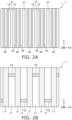
- FIGS. 2A and 2B are schematic plan views showing the semiconductor device 1 according to the embodiment.
- FIG. 2A is a plan view showing a cross section along A-A line in FIG. 1 .
- FIG. 2B is a plan view showing a cross section along B-B line in FIG. 1 .
- control electrodes 40 each extend in the Y-direction and are arranged in the X-direction.
- the third semiconductor layer 15 and the sixth semiconductor layer 21 are arranged between two adjacent control electrodes 40.
- the third semiconductor layer 15 and the sixth semiconductor layer 21 extend in the Y-direction, respectively.
- the fourth semiconductor layers 17 each extend in the Y-direction.
- the fifth semiconductor layer 19 is partially provided between the two adjacent fourth semiconductor layers 17.
- the two adjacent fourth semiconductor layers 17 are electrically connected to each other via the fifth semiconductor layer 19.
- the hole rejection via the fourth semiconductor layers 17 can be promoted, and a switching speed is improved, for example, in the turn-off process from an ON-state to an OFF-state.
- the fifth semiconductor layer 19 includes the second conductive type impurities with the concentration higher than the concentration of the second conductive type impurities of the second semiconductor layer 13. Therefore, the hole ejection resistance can be reduced in the ejection path to the second electrode 30 via the fifth semiconductor layer 19 and the second semiconductor layer 13. Thereby, an avalanche resistance can be increased around the fifth semiconductor layer 19. Further, it is also possible to increase a capacity for withstanding an overcurrent due to an external surge.
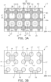
- FIGS. 3A and 3B are schematic plan views showing the semiconductor device 2 according to the first variation of the embodiment.
- FIG. 3A is a plan view showing a cross section along A-A line in FIG. 1 .
- FIG. 3B is a plan view showing a cross section along B-B line in FIG. 1 .
- the control electrode 40 includes a first portion 40a and a second portion 40b.
- the first portion 40a extends, for example, in the X-direction.
- the second portion 40b extends, for example, in the Y-direction.
- the fourth semiconductor layer 17 is shown in the drawing by a dashed line.
- the fourth semiconductor layer 17 is provided below a cross point of the first portion 40a and the second portion 40b.
- the multiple fourth semiconductor layers 17 each formed into an island shape are apart from each other.
- the fourth semiconductor layer 17 extends in the Z-direction and has, for example, a columnar shape (see FIG. 1 ).
- the third semiconductor layer 15 and the sixth semiconductor layer 21 are provided in an area surrounded by the first portion 40a and the second portion 40b of the control electrode 40.
- the sixth semiconductor layer 21 is provided, for example, at a center of the area surrounded by the control electrode 40.
- the third semiconductor layer 15 surrounds the sixth semiconductor layer 21.
- the semiconductor part 10 further includes an eighth semiconductor layer 25 of the second conductive type.
- the eighth semiconductor layer 25 is provided at another area surrounded by the first portion 40a and the second portion 40b of the control electrode 40 and covers the whole area.
- the eighth semiconductor layer 25 is a p-type contact layer different from the sixth semiconductor layer 21.
- the fifth semiconductor layer 19 is provided at a position surrounded by four fourth semiconductor layers 17.
- the fifth semiconductor layer 19 connects the four fourth semiconductor layers 17 therearound.
- the four fourth semiconductor layers 17 are electrically connected to each other via the fifth semiconductor layer 19.
- FIG. 4 is a schematic cross-sectional view showing the semiconductor device 2 according to the embodiment.
- FIG. 4 is a cross-sectional view along C-C line shown in FIG. 3A .
- the fifth semiconductor layer 19 is provided between the first semiconductor layer 11 and the second semiconductor layer 13.
- the fifth semiconductor layer 19 is partially provided on the first semiconductor layer 11.
- the eighth semiconductor layer 25 is provided between the second semiconductor layer 13 and the second electrode 30.
- the eighth semiconductor layer 25 is provided above the fifth semiconductor layer 19.
- the fourth semiconductor layers 17 are electrically connected to the second semiconductor layer 13 via the fifth semiconductor layer 19.
- the second semiconductor layer 13 is electrically connected to the second electrode 30 via the eighth semiconductor layer 25.
- the eighth semiconductor layer 25 includes a second conductive type impurity with a concentration higher than the concentration of the second conductive type impurities in the second semiconductor layer 13.
- the switching speed is improved in the turn-off process, and the capacity for withstanding an avalanche current and a surge current is improved.
- FIGS. 5A and 5B are schematic views showing the semiconductor device 3 according to the second variation of the embodiment.
- FIG. 5A is a plan view showing a cross section along A-A line shown in FIG. 1 .
- FIG. 5B is a cross-sectional view along D-D line shown in FIG. 5A .
- the multiple control electrodes 40 each extend in the Y-direction.
- the multiple control electrodes 40 are arranged in the X-direction.
- the third semiconductor layer 15 and the sixth semiconductor layer 21 are arranged in the X-direction between adjacent control electrodes 40.
- the third semiconductor layer 15 and the sixth semiconductor layer 21 each extend in the Y-direction along the control electrode 40.
- the first semiconductor layer 11 and the second semiconductor layer 13 each include a portion dividing the third semiconductor layer 15 and the sixth semiconductor layer 21. The portion of the second semiconductor layer 13 surrounds the portion of the first semiconductor layer 11.
- the first semiconductor layer 11 includes an extended portion Ilex extending into the second semiconductor layer 13 in the Z-direction.
- the extended portion Ilex contacts the second electrode 30.
- the second electrode 30 is connected to the extending portion Ilex of the first semiconductor layer 11 at the front surface 10F of the semiconductor part 10.
- the second electrode 30 is contacts the extending portion 11ex with, for example, a Schottky junction.
- the semiconductor device 3 includes the fifth semiconductor layer 19 that electrically connects the fourth semiconductor layers 17 and the second semiconductor layer 13.
- an MOS transistor and an Schottky diode are integrated.
- the Schottky diode for example, it is possible to prevent the characteristic degradation due to crystal defects extending under a bipolar operation. Whereas the crystal defects are generated more likely in SiC as compared with silicon (Si), it is possible to prevent the characteristic degradation by providing the Schottky diode.
- the high breakdown voltage provided by SiC and suppressing the characteristic degradation can be achieved.
Landscapes
- Electrodes Of Semiconductors (AREA)
- Metal-Oxide And Bipolar Metal-Oxide Semiconductor Integrated Circuits (AREA)
Abstract
A semiconductor device (1, 2, 3) includes first, second and control electrodes (20, 30, 40), and a semiconductor part (10) between the first and second electrode (20, 30). The semiconductor part (10) includes first and third layers (11, 15) of a first conductive type, and second, fourth and fifth layers (13, 17, 19) of a second conductive type. The first layer (11) extends between the first and second electrodes (20, 30). The second layer (13) is provided between the first layer (11) and the second electrode (30). The third layer (15) is partially provided on the second layer (13) between the second layer (13) and the second electrode (30). A first fourth layer (17) and a second fourth layer (17) are provided in the first layer (11). The fifth layer (19) is provided between the first layer (11) and the second layer (13). The fifth layer (19) is partially provided on the first layer (11) between the first fourth layer (17) and the second fourth layer (17). The control electrode (40) is provided between the second electrode (30) and each of the fourth layers (17).
Description
- Embodiments relate to a semiconductor device.
- It is required for a power control semiconductor device to reduce on-resistance and improve a switching speed and a current withstand.
-
-
FIG. 1 is a schematic cross-sectional view showing a semiconductor device according to an embodiment; -
FIGS. 2A and 2B are schematic plan views showing the semiconductor device according to the embodiment; -
FIGS. 3A and 3B are schematic plan views showing a semiconductor device according to a first variation of the embodiment; -
FIG. 4 is a schematic cross-sectional view showing the semiconductor device according to the first variation of the embodiment: and -
FIGS. 5A and 5B are schematic views showing a semiconductor device according to a second variation of the embodiment. - According to one embodiment, a semiconductor device includes a first electrode, a second electrode, a semiconductor part and a control electrode. The second electrode is apart from the first electrode. The semiconductor part is provided between the first electrode and the second electrode. The semiconductor part includes first to fifth semiconductor layers. The first semiconductor layer of a first conductive type extends between the first electrode and the second electrode. The second semiconductor layer of a second conductive type is provided between the first semiconductor layer and the second electrode. The third semiconductor layer of the first conductive type is partially provided on the second semiconductor layer between the second semiconductor layer and the second electrode. A plurality of fourth semiconductor layers are provided in the first semiconductor layer. The fourth semiconductor layers are of the second conductive type. The fourth semiconductor layers each extend in a first direction directed from the first electrode toward the second electrode. The fourth semiconductor layers are arranged in a second direction orthogonal to the first direction. The fourth semiconductor layers include a first fourth semiconductor layer and a second fourth semiconductor layer adjacent to each other. The fifth semiconductor layer of the second conductive type is provided between the first semiconductor layer and the second semiconductor layer. The fifth semiconductor layer being partially provided on the first semiconductor layer between the first fourth semiconductor layer and the second fourth semiconductor layer. The fifth semiconductor layer connects the first fourth semiconductor layer and the second fourth semiconductor layer. The control electrode is provided between the second electrode and each of the fourth semiconductor layers. The control electrode faces the second semiconductor layer via a first insulating film.
- Embodiments will now be described with reference to the drawings. The same portions inside the drawings are marked with the same numerals; a detailed description is omitted as appropriate; and the different portions are described. The drawings are schematic or conceptual; and the relationships between the thicknesses and widths of portions, the proportions of sizes between portions, etc., are not necessarily the same as the actual values thereof. The dimensions and/or the proportions may be illustrated differently between the drawings, even in the case where the same portion is illustrated.
- There are cases where the dispositions of the components are described using the directions of XYZ axes shown in the drawings. The X-axis, the Y-axis, and the Z-axis are orthogonal to each other. Hereinbelow, the directions of the X-axis, the Y-axis, and the Z-axis are described as an X-direction, a Y-direction, and a Z-direction. Also, there are cases where the Z-direction is described as upward and the direction opposite to the Z-direction is described as downward.
-
FIG. 1 is a schematic cross-sectional view showing asemiconductor device 1 according to an embodiment. Thesemiconductor device 1 is a MOS transistor having a so-called super junction structure. - As shown in
FIG. 1 , thesemiconductor device 1 includes asemiconductor part 10, afirst electrode 20, asecond electrode 30, and acontrol electrode 40. Thesemiconductor part 10 is provided between thefirst electrode 20 and thesecond electrode 30. Thesemiconductor part 10 is, for example, silicon carbide (SiC). Thefirst electrode 20 is provided on aback surface 10B of thesemiconductor part 10. Thefirst electrode 20 is, for example, a drain electrode. Thesecond electrode 30 is provided on afront surface 10F of thesemiconductor part 10. Thesecond electrode 30 is, for example, a source electrode. - The
semiconductor part 10 includes afirst semiconductor layer 11 of a first conductive type, asecond semiconductor layer 13 of a second conductive type, athird semiconductor layer 15 of the first conductive type, afourth semiconductor layer 17 of the second conductive type, afifth semiconductor layer 19 of the second conductive type, asixth semiconductor layer 21 of the second conductive type, and aseventh semiconductor layer 23 of the first conductive type. - Hereinafter, the first conductive type is described as an n-type and the second conductive type is described as a p-type. The
first semiconductor layer 11 is, for example, an n-type drift layer. Thesecond semiconductor layer 13 is, for example, a p-type base layer. Thethird semiconductor layer 15 is, for example, an n-type source layer. Thesixth semiconductor layer 21 is, for example, a p-type contact layer. Theseventh semiconductor layer 23 is, for example, an n-type buffer layer. The embodiment is not limited to the example and, for example, may be a structure in which an n-type substrate is interposed between theseventh semiconductor layer 23 and thefirst electrode 20. - The
control electrode 40 is provided in thesemiconductor part 10, and is electrically insulated from thesemiconductor part 10 by a firstinsulating film 43. Thecontrol electrode 40 is, for example, a gate electrode. The firstinsulating film 43 is a gate insulating film. Thecontrol electrode 40 are provided inside a trench TR. The trench TR is provided on afront surface 10F side of thesemiconductor part 10. - For example, the
control electrode 40 is provided between thefirst electrode 20 and thesecond electrode 30. A secondinsulating film 45 is provided between thesecond electrode 30 and thecontrol electrodes 40. Thecontrol electrode 40 is electrically insulated from thesecond electrode 30 by the secondinsulating film 45. The secondinsulating film 45 is, for example, an interlayer insulating film. - The
first semiconductor layer 11 extends between thefirst electrode 20 and thesecond electrode 30. Thesecond semiconductor layer 13 is provided between thefirst semiconductor layer 11 and thesecond electrode 30. Thethird semiconductor layer 15 is partially provided between thesecond semiconductor layer 13 and thesecond electrode 30. - As shown in
FIG. 1 , thefourth semiconductor layer 17 is provided in thefirst semiconductor layer 11. The fourth semiconductor layers 17 extends in a first direction directed from thefirst electrode 20 toward thesecond electrode 30, for example, in the Z-direction. - The
semiconductor device 1 includes a plurality of the fourth semiconductor layers 17 and a plurality of thecontrol electrodes 40. The fourth semiconductor layers 17 are arranged in a second direction orthogonal to the first direction, for example, in the X-direction. A so-called super junction structure is configured in thefirst semiconductor layer 11 by the fourth semiconductor layers 17. That is, a portion of thefirst semiconductor layer 11 and thefourth semiconductor layer 17 are alternately arranged in the X-direction. - The
control electrode 40 is provided between each of the fourth semiconductor layers 17 and thesecond electrode 30. Thecontrol electrode 40 faces thesecond semiconductor layer 13 via the first insulatingfilm 43 in the X-direction. Thethird semiconductor layer 15 is in contact with the first insulatingfilm 43. Thesecond semiconductor layer 13 faces thecontrol electrodes 40 between thefirst semiconductor layer 11 and thethird semiconductor layer 15. - The
fifth semiconductor layer 19 is partially provided between thefirst semiconductor layer 11 and thesecond semiconductor layer 13. Thefifth semiconductor layer 19 is provided between two adjacent fourth semiconductor layers 17. Thefifth semiconductor layer 19 is connected to the two adjacent fourth semiconductor layers 17. Thefifth semiconductor layer 19 is in contact with thesecond semiconductor layer 13. That is, thefifth semiconductor layer 19 electrically connects the two adjacent fourth semiconductor layers 17 and thesecond semiconductor layer 13. - The
fifth semiconductor layer 19 includes, for example, a second conductive type impurity with a concentration higher than a concentration of a second conductive type impurity in thesecond semiconductor layer 13. Thefifth semiconductor layer 19 includes, for example, the second conductive type impurity with the concentration higher than a concentration of a second conductive type impurity in thefourth semiconductor layer 17. - The
sixth semiconductor layer 21 is partially provided on thesecond semiconductor layer 13 between thesecond semiconductor layer 13 and thesecond electrode 30. Thethird semiconductor layer 15 and thesixth semiconductor layer 21 are arranged, for example, in the X-direction on thesecond semiconductor layer 13. - The
second electrode 30 is connected to thethird semiconductor layer 15 and thesixth semiconductor layer 21, for example, at thefront surface 10F of thesemiconductor part 10. Thesecond electrode 30 is connected to thethird semiconductor layer 15 and thesixth semiconductor layer 21 with, for example, an Ohmic junction. Thesecond electrode 30 is electrically connected to thesecond semiconductor layer 13 via thesixth semiconductor layer 21. - The
seventh semiconductor layer 23 is provided between thefirst semiconductor layer 11 and thefirst electrode 20. Theseventh semiconductor layer 23 includes a first conductive type impurity with a concentration higher than a concentration of a first conductive type impurity in thefirst semiconductor layer 11. Thefirst semiconductor layer 11 includes another portion provided between each of the fourth semiconductor layers 17 and theseventh semiconductor layer 23. -
FIGS. 2A and 2B are schematic plan views showing thesemiconductor device 1 according to the embodiment.FIG. 2A is a plan view showing a cross section along A-A line inFIG. 1 .FIG. 2B is a plan view showing a cross section along B-B line inFIG. 1 . - As shown in
FIG. 2A , thecontrol electrodes 40 each extend in the Y-direction and are arranged in the X-direction. Thethird semiconductor layer 15 and thesixth semiconductor layer 21 are arranged between twoadjacent control electrodes 40. Thethird semiconductor layer 15 and thesixth semiconductor layer 21 extend in the Y-direction, respectively. - As shown in
FIG. 2B , the fourth semiconductor layers 17 each extend in the Y-direction. Thefifth semiconductor layer 19 is partially provided between the two adjacent fourth semiconductor layers 17. The two adjacent fourth semiconductor layers 17 are electrically connected to each other via thefifth semiconductor layer 19. - Accordingly, by providing the
fifth semiconductor layer 19 between the two adjacent fourth semiconductor layers 17, the hole rejection via the fourth semiconductor layers 17 can be promoted, and a switching speed is improved, for example, in the turn-off process from an ON-state to an OFF-state. - The
fifth semiconductor layer 19 includes the second conductive type impurities with the concentration higher than the concentration of the second conductive type impurities of thesecond semiconductor layer 13. Therefore, the hole ejection resistance can be reduced in the ejection path to thesecond electrode 30 via thefifth semiconductor layer 19 and thesecond semiconductor layer 13. Thereby, an avalanche resistance can be increased around thefifth semiconductor layer 19. Further, it is also possible to increase a capacity for withstanding an overcurrent due to an external surge. - Next, a
semiconductor device 2 according to a first variation of the embodiment will be described.FIGS. 3A and 3B are schematic plan views showing thesemiconductor device 2 according to the first variation of the embodiment.FIG. 3A is a plan view showing a cross section along A-A line inFIG. 1 .FIG. 3B is a plan view showing a cross section along B-B line inFIG. 1 . - As shown in
FIG. 3A , thecontrol electrode 40 includes afirst portion 40a and asecond portion 40b. Thefirst portion 40a extends, for example, in the X-direction. Thesecond portion 40b extends, for example, in the Y-direction. Thefourth semiconductor layer 17 is shown in the drawing by a dashed line. Thefourth semiconductor layer 17 is provided below a cross point of thefirst portion 40a and thesecond portion 40b. The multiple fourth semiconductor layers 17 each formed into an island shape are apart from each other. Thefourth semiconductor layer 17 extends in the Z-direction and has, for example, a columnar shape (seeFIG. 1 ). - The
third semiconductor layer 15 and thesixth semiconductor layer 21 are provided in an area surrounded by thefirst portion 40a and thesecond portion 40b of thecontrol electrode 40. Thesixth semiconductor layer 21 is provided, for example, at a center of the area surrounded by thecontrol electrode 40. Thethird semiconductor layer 15 surrounds thesixth semiconductor layer 21. Thesemiconductor part 10 further includes aneighth semiconductor layer 25 of the second conductive type. Theeighth semiconductor layer 25 is provided at another area surrounded by thefirst portion 40a and thesecond portion 40b of thecontrol electrode 40 and covers the whole area. Theeighth semiconductor layer 25 is a p-type contact layer different from thesixth semiconductor layer 21. - As shown in
FIG. 3B , thefifth semiconductor layer 19 is provided at a position surrounded by four fourth semiconductor layers 17. Thefifth semiconductor layer 19 connects the fourfourth semiconductor layers 17 therearound. The four fourth semiconductor layers 17 are electrically connected to each other via thefifth semiconductor layer 19. -
FIG. 4 is a schematic cross-sectional view showing thesemiconductor device 2 according to the embodiment.FIG. 4 is a cross-sectional view along C-C line shown inFIG. 3A . - As shown in
FIG. 4 , thefifth semiconductor layer 19 is provided between thefirst semiconductor layer 11 and thesecond semiconductor layer 13. Thefifth semiconductor layer 19 is partially provided on thefirst semiconductor layer 11. Theeighth semiconductor layer 25 is provided between thesecond semiconductor layer 13 and thesecond electrode 30. Theeighth semiconductor layer 25 is provided above thefifth semiconductor layer 19. - The fourth semiconductor layers 17 are electrically connected to the
second semiconductor layer 13 via thefifth semiconductor layer 19. Thesecond semiconductor layer 13 is electrically connected to thesecond electrode 30 via theeighth semiconductor layer 25. Theeighth semiconductor layer 25 includes a second conductive type impurity with a concentration higher than the concentration of the second conductive type impurities in thesecond semiconductor layer 13. - Also in the example, by providing the
fifth semiconductor layer 19, the switching speed is improved in the turn-off process, and the capacity for withstanding an avalanche current and a surge current is improved. - A
semiconductor device 3 according to a second variation of the embodiment is described below.FIGS. 5A and 5B are schematic views showing thesemiconductor device 3 according to the second variation of the embodiment.FIG. 5A is a plan view showing a cross section along A-A line shown inFIG. 1 .FIG. 5B is a cross-sectional view along D-D line shown inFIG. 5A . - As shown in
FIG. 5A , themultiple control electrodes 40 each extend in the Y-direction. Themultiple control electrodes 40 are arranged in the X-direction. Thethird semiconductor layer 15 and thesixth semiconductor layer 21 are arranged in the X-direction betweenadjacent control electrodes 40. Thethird semiconductor layer 15 and thesixth semiconductor layer 21 each extend in the Y-direction along thecontrol electrode 40. Further, between theadjacent control electrodes 40, thefirst semiconductor layer 11 and thesecond semiconductor layer 13 each include a portion dividing thethird semiconductor layer 15 and thesixth semiconductor layer 21. The portion of thesecond semiconductor layer 13 surrounds the portion of thefirst semiconductor layer 11. - As shown in
FIG. 5B , thefirst semiconductor layer 11 includes an extended portion Ilex extending into thesecond semiconductor layer 13 in the Z-direction. The extended portion Ilex contacts thesecond electrode 30. Thesecond electrode 30 is connected to the extending portion Ilex of thefirst semiconductor layer 11 at thefront surface 10F of thesemiconductor part 10. Thesecond electrode 30 is contacts the extending portion 11ex with, for example, a Schottky junction. - As described above, the
semiconductor device 3 includes thefifth semiconductor layer 19 that electrically connects the fourth semiconductor layers 17 and thesecond semiconductor layer 13. In thesemiconductor device 3, an MOS transistor and an Schottky diode are integrated. By providing the Schottky diode, for example, it is possible to prevent the characteristic degradation due to crystal defects extending under a bipolar operation. Whereas the crystal defects are generated more likely in SiC as compared with silicon (Si), it is possible to prevent the characteristic degradation by providing the Schottky diode. Thus, in thesemiconductor device 3, the high breakdown voltage provided by SiC and suppressing the characteristic degradation can be achieved. - While certain embodiments have been described, these embodiments have been presented by way of example only, and are not intended to limit the scope of the inventions. Indeed, the novel embodiments described herein may be embodied in a variety of other forms; furthermore, various omissions, substitutions and changes in the form of the embodiments described herein may be made without departing from the spirit of the inventions. The accompanying claims and their equivalents are intended to cover such forms or modifications as would fall within the scope of the invention.
- It is explicitly stated that all features disclosed in the description and/or the claims are intended to be disclosed separately and independently from each other for the purpose of original disclosure as well as for the purpose of restricting the claimed invention independent of the composition of the features in the embodiments and/or the claims. It is explicitly stated that all value ranges or indications of groups of entities disclose every possible intermediate value or intermediate entity for the purpose of original disclosure as well as for the purpose of restricting the claimed invention, in particular as limits of value ranges.
Claims (14)
- A semiconductor device (1, 2, 3), comprising:a first electrode (20);a second electrode (30) apart from the first electrode (20);a semiconductor part (10) provided between the first electrode (20) and the second electrode (30), the semiconductor part (10) including first to fifth semiconductor layers (11, 13, 15, 17, 19),the first semiconductor layer (11) of a first conductive type extending between the first electrode (20) and the second electrode (30),the second semiconductor layer (13) of a second conductive type being provided between the first semiconductor layer (11) and the second electrode (30),the third semiconductor layer (15) of the first conductive type being partially provided on the second semiconductor layer (13) between the second semiconductor layer (13) and the second electrode (30),a plurality of fourth semiconductor layers (17) being provided in the first semiconductor layer (11), the fourth semiconductor layers (17) being of the second conductive type, the fourth semiconductor layers (17) each extending in a first direction (Z) directed from the first electrode (20) toward the second electrode (30) and being arranged in a second direction (X) orthogonal to the first direction (Z), the fourth semiconductor layers (17) including a first fourth semiconductor layer (17) and a second fourth semiconductor layer (17) adjacent to each other, andthe fifth semiconductor layer (19) of the second conductive type being provided between the first semiconductor layer (11) and the second semiconductor layer (13), the fifth semiconductor layer (19) being partially provided on the first semiconductor layer (11) between the first fourth semiconductor layer (17) and the second fourth semiconductor layer (17), the fifth semiconductor layer (19) connecting the first fourth semiconductor layer (17) and the second fourth semiconductor layer (17); anda control electrode (40) provided between the second electrode (30) and each of the fourth semiconductor layers (17), the control electrode (40) facing the second semiconductor layer (13) via a first insulating film (43).
- The device (1, 2, 3) according to claim 1, wherein
the first fourth semiconductor layer (17) and the second fourth semiconductor layer (17) are electrically connected to the second semiconductor layer (13) via the fifth semiconductor layer (19). - The device (1, 2, 3) according to claim 1 or 2, wherein
the fifth semiconductor layer (19) includes a second conductive type impurity with a concentration higher than a concentration of a second conductive type impurity in the second semiconductor layer (13). - The device (1, 2, 3) according to any one of claims 1 to 3, whereinthe semiconductor part (10) further includes a sixth semiconductor layer (21) of the second conductive type partially provided on the second semiconductor layer (13) between the second semiconductor layer (13) and the second electrode (30), the third semiconductor layer (15) and the sixth semiconductor layer (21) being arranged along the second semiconductor layer (13), andthe second semiconductor layer (13) is electrically connected to the second electrode (30) via the sixth semiconductor layer (21).
- The device (1, 2, 3) according to any one of claims 1 to 4, whereinthe semiconductor part (10) further includes a seventh semiconductor layer (23) of the first conductive type, the seventh semiconductor layer (23) being provided between the first semiconductor layer (11) and the first electrode (20), the seventh semiconductor layer (23) including a first conductive type impurity with a concentration higher than a concentration of the first conductive type impurity in the first semiconductor layer (11), andthe first semiconductor layer (11) includes a portion provided between the fourth semiconductor layers (17) and the seventh semiconductor layer (23).
- The device (1, 3) according to any one of claims 1 to 5, wherein
the control electrode (40) extends in a third direction (Y) orthogonal to the first direction (Z) and the second direction (X). - The device (1, 3) according to claim 6, wherein
the plurality of fourth semiconductor layers (17) each extends in the third direction (Y). - The device (2) according to any one of claims 1 to 5, whereinthe control electrode (40) includes a first portion (40a) extending in the second direction (X) and a second portion (40b) extending in a third direction (Y) orthogonal to the first direction (Z) and the second direction (Y), andthe plurality of fourth semiconductor layers (17) each are provided below a cross point of the first portion (40a) and the second portion (40b) of the control electrode (40).
- The device (2) according to claim 8, wherein
the plurality of fourth semiconductor layers (17) each are provided in a columnar shape extending in the first direction (Z). - The device (3) according to any one of claims 1 to 7, wherein
the first semiconductor layer (11) extends into the second semiconductor layer (13) in the first direction (Z) and includes an extended portion (11ex) in contact with the second electrode (30). - The device (3) according to claim 10, wherein
the second semiconductor layer (13) surrounds the extended portion (11ex) of the first semiconductor layer (11) and is in contact with the second electrode (30). - The device (1, 2, 3) according to any one of claims 1 to 11, whereinthe third semiconductor layer (15) is in contact with the first insulating film (43), andthe second semiconductor layer (13) faces the control electrode (40) via the first insulating film (43) between the first semiconductor layer (11) and the third semiconductor layer (15).
- The device (1, 2, 3) according to any one of claims 1 to 12, wherein
the control electrode (40) is provided inside a trench (TR) having an opening at the second electrode (20) side of the semiconductor part (10), and is electrically insulated from the semiconductor part (10) by a second insulating film (45). - The device (1, 3) according to claim 13, whereina plurality of the control electrodes (40) are arranged in the second direction (X), andthe fifth semiconductor layer (17) is partially provided on the first semiconductor later (11) between two control electrodes (40) adjacent to each other in the second direction (X).
Applications Claiming Priority (1)
| Application Number | Priority Date | Filing Date | Title |
|---|---|---|---|
| JP2022043923A JP7703474B2 (en) | 2022-03-18 | 2022-03-18 | Semiconductor Device |
Publications (1)
| Publication Number | Publication Date |
|---|---|
| EP4246586A1 true EP4246586A1 (en) | 2023-09-20 |
Family
ID=83271252
Family Applications (1)
| Application Number | Title | Priority Date | Filing Date |
|---|---|---|---|
| EP22190531.8A Pending EP4246586A1 (en) | 2022-03-18 | 2022-08-16 | Semiconductor device |
Country Status (4)
| Country | Link |
|---|---|
| US (1) | US12513923B2 (en) |
| EP (1) | EP4246586A1 (en) |
| JP (1) | JP7703474B2 (en) |
| CN (1) | CN116799061A (en) |
Families Citing this family (1)
| Publication number | Priority date | Publication date | Assignee | Title |
|---|---|---|---|---|
| JP7703474B2 (en) * | 2022-03-18 | 2025-07-07 | 株式会社東芝 | Semiconductor Device |
Citations (5)
| Publication number | Priority date | Publication date | Assignee | Title |
|---|---|---|---|---|
| JP2005333068A (en) * | 2004-05-21 | 2005-12-02 | Toshiba Corp | Semiconductor device |
| US20100096692A1 (en) * | 2008-10-16 | 2010-04-22 | Kabushiki Kaisha Toshiba | Semiconductor device |
| US7928470B2 (en) * | 2005-11-25 | 2011-04-19 | Denso Corporation | Semiconductor device having super junction MOS transistor and method for manufacturing the same |
| US20150333168A1 (en) * | 2014-05-14 | 2015-11-19 | Infineon Technologies Austria Ag | Semiconductor device with field dielectric in an edge area |
| JP2016119392A (en) * | 2014-12-22 | 2016-06-30 | 日産自動車株式会社 | Insulated gate type semiconductor device and method of manufacturing the same |
Family Cites Families (31)
| Publication number | Priority date | Publication date | Assignee | Title |
|---|---|---|---|---|
| JP2008066708A (en) * | 2006-08-09 | 2008-03-21 | Toshiba Corp | Semiconductor device |
| JP2011009387A (en) | 2009-06-24 | 2011-01-13 | Renesas Electronics Corp | Semiconductor device, method of manufacturing the same, and dc-dc converter using the same |
| JP5672708B2 (en) | 2010-02-03 | 2015-02-18 | 株式会社デンソー | Semiconductor device provided with vertical semiconductor element |
| US9337271B2 (en) * | 2012-12-28 | 2016-05-10 | Mitsubishi Electric Corporation | Silicon-carbide semiconductor device and manufacturing method therefor |
| JP6471508B2 (en) * | 2015-01-19 | 2019-02-20 | 富士電機株式会社 | Semiconductor device |
| JP6536377B2 (en) | 2015-11-24 | 2019-07-03 | 株式会社豊田自動織機 | Semiconductor device |
| US20210043735A1 (en) * | 2016-04-07 | 2021-02-11 | Abb Power Grids Switzerland Ag | Short channel trench power mosfet and method |
| DE112017002020B4 (en) * | 2016-04-14 | 2023-03-02 | National Institute Of Advanced Industrial Science And Technology | SILICON CARBIDE SEMICONDUCTOR DEVICE AND METHOD OF MAKING THE SAME |
| CN110709997B (en) | 2017-06-06 | 2023-02-28 | 三菱电机株式会社 | Semiconductor device and power conversion device |
| DE112018007114B4 (en) * | 2018-02-19 | 2025-04-03 | Mitsubishi Electric Corporation | SILICON CARBIDE SEMICONDUCTOR UNIT |
| DE112018007106B4 (en) * | 2018-02-19 | 2026-03-05 | Mitsubishi Electric Corporation | SILICON CARBIDE SEMICONDUCER UNIT |
| JP7119814B2 (en) * | 2018-09-14 | 2022-08-17 | 富士電機株式会社 | Silicon carbide semiconductor device and method for manufacturing silicon carbide semiconductor device |
| JP7230434B2 (en) * | 2018-10-30 | 2023-03-01 | 富士電機株式会社 | Semiconductor device manufacturing method |
| JP7275573B2 (en) * | 2018-12-27 | 2023-05-18 | 富士電機株式会社 | Silicon carbide semiconductor device and method for manufacturing silicon carbide semiconductor device |
| JP7371335B2 (en) * | 2019-03-13 | 2023-10-31 | 富士電機株式会社 | semiconductor equipment |
| JP6992021B2 (en) * | 2019-03-18 | 2022-01-13 | 株式会社東芝 | Semiconductor devices, inverter circuits, drives, vehicles, and elevators |
| JP7310343B2 (en) * | 2019-06-14 | 2023-07-19 | 富士電機株式会社 | semiconductor equipment |
| JP7263178B2 (en) | 2019-08-02 | 2023-04-24 | 株式会社東芝 | Semiconductor devices, inverter circuits, drive devices, vehicles, and elevators |
| US20210050420A1 (en) * | 2019-08-13 | 2021-02-18 | Semiconductor Components Industries, Llc | Silicon carbide trench power device |
| JP7389239B2 (en) * | 2019-09-10 | 2023-11-29 | コリア エレクトロテクノロジー リサーチ インスティテュート | Trench gate type SiCMOSFET device and its manufacturing method |
| JP7462394B2 (en) * | 2019-09-10 | 2024-04-05 | 富士電機株式会社 | Silicon carbide semiconductor device and method for manufacturing silicon carbide semiconductor device |
| WO2022025010A1 (en) * | 2020-07-29 | 2022-02-03 | 富士電機株式会社 | Silicon carbide semiconductor device |
| US12057482B2 (en) * | 2020-08-11 | 2024-08-06 | Maxpower Semiconductor, Inc. | MOSFET with distributed doped P-shield zones under trenches |
| US11462638B2 (en) * | 2020-10-19 | 2022-10-04 | Nami MOS CO., LTD. | SiC super junction trench MOSFET |
| US12080790B2 (en) * | 2020-10-28 | 2024-09-03 | Wolfspeed, Inc. | Power semiconductor devices including angled gate trenches |
| JP7729033B2 (en) * | 2020-11-24 | 2025-08-26 | 富士電機株式会社 | Silicon carbide semiconductor device, semiconductor package, and method for inspecting silicon carbide semiconductor device |
| JP7582733B2 (en) * | 2020-12-15 | 2024-11-13 | 富士電機株式会社 | Vertical MOSFET with trench gate structure made of silicon carbide |
| JP7476132B2 (en) * | 2021-03-23 | 2024-04-30 | 株式会社東芝 | Semiconductor device, inverter circuit, drive device, vehicle, and elevator |
| US11777000B2 (en) * | 2021-05-17 | 2023-10-03 | Nami MOS CO., LTD. | SiC trench MOSFET with low on-resistance and switching loss |
| JP7703474B2 (en) * | 2022-03-18 | 2025-07-07 | 株式会社東芝 | Semiconductor Device |
| JP7746206B2 (en) * | 2022-03-23 | 2025-09-30 | 株式会社東芝 | Semiconductor Devices |
-
2022
- 2022-03-18 JP JP2022043923A patent/JP7703474B2/en active Active
- 2022-06-30 CN CN202210767695.0A patent/CN116799061A/en active Pending
- 2022-08-16 EP EP22190531.8A patent/EP4246586A1/en active Pending
- 2022-08-18 US US17/890,489 patent/US12513923B2/en active Active
Patent Citations (5)
| Publication number | Priority date | Publication date | Assignee | Title |
|---|---|---|---|---|
| JP2005333068A (en) * | 2004-05-21 | 2005-12-02 | Toshiba Corp | Semiconductor device |
| US7928470B2 (en) * | 2005-11-25 | 2011-04-19 | Denso Corporation | Semiconductor device having super junction MOS transistor and method for manufacturing the same |
| US20100096692A1 (en) * | 2008-10-16 | 2010-04-22 | Kabushiki Kaisha Toshiba | Semiconductor device |
| US20150333168A1 (en) * | 2014-05-14 | 2015-11-19 | Infineon Technologies Austria Ag | Semiconductor device with field dielectric in an edge area |
| JP2016119392A (en) * | 2014-12-22 | 2016-06-30 | 日産自動車株式会社 | Insulated gate type semiconductor device and method of manufacturing the same |
Also Published As
| Publication number | Publication date |
|---|---|
| US12513923B2 (en) | 2025-12-30 |
| JP2023137644A (en) | 2023-09-29 |
| CN116799061A (en) | 2023-09-22 |
| JP7703474B2 (en) | 2025-07-07 |
| US20230299212A1 (en) | 2023-09-21 |
Similar Documents
| Publication | Publication Date | Title |
|---|---|---|
| US9887285B1 (en) | Semiconductor device | |
| JP6416062B2 (en) | Semiconductor device | |
| US10727225B2 (en) | IGBT semiconductor device | |
| JP7353925B2 (en) | semiconductor equipment | |
| US10700184B2 (en) | Semiconductor device | |
| US10103222B2 (en) | Semiconductor device | |
| JP2019169595A (en) | Semiconductor device | |
| US10340378B1 (en) | Semiconductor device | |
| EP4246586A1 (en) | Semiconductor device | |
| JP7841254B2 (en) | Silicon carbide semiconductor equipment | |
| JP2016207829A (en) | Insulated gate type switching element | |
| US12588228B2 (en) | Semiconductor device | |
| US20240321963A1 (en) | Semiconductor device | |
| US12419068B2 (en) | Semiconductor device | |
| JP6782213B2 (en) | Semiconductor device | |
| CN119968937A (en) | Semiconductor devices | |
| US11257937B2 (en) | Semiconductor device | |
| JP2024137200A (en) | Field-effect transistor | |
| CN115917755B (en) | Silicon carbide semiconductor device | |
| JP2024071184A (en) | Silicon carbide semiconductor device | |
| US20260090075A1 (en) | Semiconductor device | |
| US20240321862A1 (en) | Semiconductor device | |
| US20230261105A1 (en) | Semiconductor device | |
| US20260090054A1 (en) | Semiconductor device with field plate structure | |
| US20250056869A1 (en) | Wide band gap semiconductor device |
Legal Events
| Date | Code | Title | Description |
|---|---|---|---|
| PUAI | Public reference made under article 153(3) epc to a published international application that has entered the european phase |
Free format text: ORIGINAL CODE: 0009012 |
|
| STAA | Information on the status of an ep patent application or granted ep patent |
Free format text: STATUS: REQUEST FOR EXAMINATION WAS MADE |
|
| 17P | Request for examination filed |
Effective date: 20220816 |
|
| AK | Designated contracting states |
Kind code of ref document: A1 Designated state(s): AL AT BE BG CH CY CZ DE DK EE ES FI FR GB GR HR HU IE IS IT LI LT LU LV MC MK MT NL NO PL PT RO RS SE SI SK SM TR |