EP4246469A2 - Laminated structure, display panel and electronic device - Google Patents
Laminated structure, display panel and electronic device Download PDFInfo
- Publication number
- EP4246469A2 EP4246469A2 EP23170685.4A EP23170685A EP4246469A2 EP 4246469 A2 EP4246469 A2 EP 4246469A2 EP 23170685 A EP23170685 A EP 23170685A EP 4246469 A2 EP4246469 A2 EP 4246469A2
- Authority
- EP
- European Patent Office
- Prior art keywords
- light
- layer
- absorption axis
- linear polarizing
- protective layer
- Prior art date
- Legal status (The legal status is an assumption and is not a legal conclusion. Google has not performed a legal analysis and makes no representation as to the accuracy of the status listed.)
- Granted
Links
Images






Classifications
-
- G—PHYSICS
- G06—COMPUTING OR CALCULATING; COUNTING
- G06V—IMAGE OR VIDEO RECOGNITION OR UNDERSTANDING
- G06V40/00—Recognition of biometric, human-related or animal-related patterns in image or video data
- G06V40/10—Human or animal bodies, e.g. vehicle occupants or pedestrians; Body parts, e.g. hands
- G06V40/12—Fingerprints or palmprints
- G06V40/13—Sensors therefor
- G06V40/1318—Sensors therefor using electro-optical elements or layers, e.g. electroluminescent sensing
-
- G—PHYSICS
- G06—COMPUTING OR CALCULATING; COUNTING
- G06V—IMAGE OR VIDEO RECOGNITION OR UNDERSTANDING
- G06V40/00—Recognition of biometric, human-related or animal-related patterns in image or video data
- G06V40/10—Human or animal bodies, e.g. vehicle occupants or pedestrians; Body parts, e.g. hands
- G06V40/12—Fingerprints or palmprints
- G06V40/13—Sensors therefor
- G06V40/1324—Sensors therefor by using geometrical optics, e.g. using prisms
-
- G—PHYSICS
- G02—OPTICS
- G02B—OPTICAL ELEMENTS, SYSTEMS OR APPARATUS
- G02B1/00—Optical elements characterised by the material of which they are made; Optical coatings for optical elements
- G02B1/10—Optical coatings produced by application to, or surface treatment of, optical elements
- G02B1/14—Protective coatings, e.g. hard coatings
-
- G—PHYSICS
- G02—OPTICS
- G02B—OPTICAL ELEMENTS, SYSTEMS OR APPARATUS
- G02B27/00—Optical systems or apparatus not provided for by any of the groups G02B1/00 - G02B26/00, G02B30/00
- G02B27/28—Optical systems or apparatus not provided for by any of the groups G02B1/00 - G02B26/00, G02B30/00 for polarising
- G02B27/286—Optical systems or apparatus not provided for by any of the groups G02B1/00 - G02B26/00, G02B30/00 for polarising for controlling or changing the state of polarisation, e.g. transforming one polarisation state into another
-
- G—PHYSICS
- G02—OPTICS
- G02B—OPTICAL ELEMENTS, SYSTEMS OR APPARATUS
- G02B5/00—Optical elements other than lenses
- G02B5/30—Polarising elements
- G02B5/3025—Polarisers, i.e. arrangements capable of producing a definite output polarisation state from an unpolarised input state
- G02B5/3033—Polarisers, i.e. arrangements capable of producing a definite output polarisation state from an unpolarised input state in the form of a thin sheet or foil, e.g. Polaroid
-
- G—PHYSICS
- G02—OPTICS
- G02B—OPTICAL ELEMENTS, SYSTEMS OR APPARATUS
- G02B5/00—Optical elements other than lenses
- G02B5/30—Polarising elements
- G02B5/3083—Birefringent or phase retarding elements
-
- G—PHYSICS
- G02—OPTICS
- G02F—OPTICAL DEVICES OR ARRANGEMENTS FOR THE CONTROL OF LIGHT BY MODIFICATION OF THE OPTICAL PROPERTIES OF THE MEDIA OF THE ELEMENTS INVOLVED THEREIN; NON-LINEAR OPTICS; FREQUENCY-CHANGING OF LIGHT; OPTICAL LOGIC ELEMENTS; OPTICAL ANALOGUE/DIGITAL CONVERTERS
- G02F1/00—Devices or arrangements for the control of the intensity, colour, phase, polarisation or direction of light arriving from an independent light source, e.g. switching, gating or modulating; Non-linear optics
- G02F1/01—Devices or arrangements for the control of the intensity, colour, phase, polarisation or direction of light arriving from an independent light source, e.g. switching, gating or modulating; Non-linear optics for the control of the intensity, phase, polarisation or colour
- G02F1/13—Devices or arrangements for the control of the intensity, colour, phase, polarisation or direction of light arriving from an independent light source, e.g. switching, gating or modulating; Non-linear optics for the control of the intensity, phase, polarisation or colour based on liquid crystals, e.g. single liquid crystal display cells
- G02F1/133—Constructional arrangements; Operation of liquid crystal cells; Circuit arrangements
- G02F1/1333—Constructional arrangements; Manufacturing methods
- G02F1/1335—Structural association of cells with optical devices, e.g. polarisers or reflectors
- G02F1/133528—Polarisers
-
- G—PHYSICS
- G09—EDUCATION; CRYPTOGRAPHY; DISPLAY; ADVERTISING; SEALS
- G09F—DISPLAYING; ADVERTISING; SIGNS; LABELS OR NAME-PLATES; SEALS
- G09F9/00—Indicating arrangements for variable information in which the information is built-up on a support by selection or combination of individual elements
-
- G—PHYSICS
- G02—OPTICS
- G02F—OPTICAL DEVICES OR ARRANGEMENTS FOR THE CONTROL OF LIGHT BY MODIFICATION OF THE OPTICAL PROPERTIES OF THE MEDIA OF THE ELEMENTS INVOLVED THEREIN; NON-LINEAR OPTICS; FREQUENCY-CHANGING OF LIGHT; OPTICAL LOGIC ELEMENTS; OPTICAL ANALOGUE/DIGITAL CONVERTERS
- G02F2201/00—Constructional arrangements not provided for in groups G02F1/00 - G02F7/00
- G02F2201/50—Protective arrangements
Definitions
- the present invention relates to the field of display technologies, and in particular, to a laminated structure, a display panel, and an electronic device.
- a technical problem to be resolved by embodiments of this application is about a laminated structure, a display panel, and an electronic device that can improve the stability of light transmission.
- an implementation of this application provides a laminated structure, including a protective layer, a linear polarizing layer, and a quarter-wave plate that are laminated in sequence.
- the protective layer is used to polarize light to form linearly polarized light.
- An angle between an absorption axis of the protective layer and an absorption axis of the linear polarizing layer is zero degrees.
- An angle between the absorption axis of the linear polarizing layer and an absorption axis of the quarter-wave plate is 45 degrees.
- the angle between the absorption axis of the linear polarizing layer and the absorption axis of the protective layer is zero degrees, and there is no difference between a direction of the absorption axis of the protective layer and a direction of the absorption axis of the linear polarizing layer. Therefore, a luminous flux of light passing through the protective layer is roughly the same as that of light passing through the linear polarizing layer. In other words, the light intensity of the light passing through the protective layer is consistent with that of the light passing through the linear polarizing layer.
- the light loss during light transmission in the laminated structure can be reduced, and the stability of light transmission in the laminated structure can be improved, to stabilize the light intensity of light passing through the laminated structure, and improve the stability of light entering an optical fingerprint recognition module, thereby improving recognition precision of the optical fingerprint recognition module.
- the laminated structure further includes a reinforcing layer, and the reinforcing layer is arranged between the protective layer and the linear polarizing layer, and used to protect the laminated structure and enhance the strength of the laminated structure.
- the material strength of the reinforcing layer is greater than that of the protective layer.
- the reinforcing layer is made of an isotropic material, to reduce the light loss during light transmission in the laminated structure, and enhance the stability of light transmission.
- the linear polarizing layer is fixed to the reinforcing layer through an optical adhesive layer, to improve the bonding strength between the linear polarizing layer and the reinforcing layer.
- the optical adhesive layer is made of an isotropic material, to further reduce the light loss during light transmission in the laminated structure, and enhance the stability of light transmission.
- the reinforcing layer is a glass cover plate, to enhance the strength and protection performance of the laminated structure; and the protective layer is a film layer attached to one side of the reinforcing layer away from the linear polarizing layer, to prevent the reinforcing layer from being scratched and worn.
- the reinforcing layer is used to polarize light to form linearly polarized light.
- An angle between an absorption axis of the reinforcing layer and the absorption axis of the linear polarizing layer is zero degrees.
- the reinforcing layer is set as a laminated layer in a direction consistent with the direction of the absorption axis of the linear polarizing layer, so that the optical performance of the reinforcing layer, the protective layer, and the linear polarizing layer can be matched, and the light intensity of light passing through the protective layer is consistent with that of light passing through the reinforcing layer and the linear polarizing layer, thereby enhancing the stability of light transmission.
- the protective layer is a cover plate, and the protective layer is made of a material including one of ceramic and plastic, helping reduce a thickness of the laminated structure while increasing the strength of the protective layer.
- the protective layer is made of materials including polyethylene terephthalate plastic and thermoplastic polyurethane elastomer rubber.
- this application further provides a display panel, applied to an electronic device with an optical fingerprint recognition module.
- the display panel includes a functional substrate and the foregoing laminated structure that are laminated.
- the functional substrate is located on one side of a quarter-wave plate away from a protective layer, and the functional substrate has a light-transmitting area, to allow light emitted from the quarter-wave plate to enter the optical fingerprint recognition module through the light-transmitting area.
- an angle between an absorption axis of the protective layer located on an outermost side of the display panel and an absorption axis of a linear polarizing layer is zero degrees, and there is no difference between a direction of the absorption axis of the protective layer and a direction of the absorption axis of the linear polarizing layer. Therefore, a luminous flux of light passing through the protective layer is roughly the same as that of light passing through the linear polarizing layer. In other words, the light intensity of light passing through the protective layer is consistent with that of light passing through the linear polarizing layer.
- the light loss during light transmission in the display panel can be reduced, and the stability of light transmission in the display panel can be improved, to stabilize the light intensity of light entering the optical fingerprint recognition module through the light-transmitting area of the functional substrate, and improve the stability of light entering the optical fingerprint recognition module, thereby improving the recognition precision of the optical fingerprint recognition module.
- the linearly polarized light passing through the protective layer becomes circularly polarized light passing through the linear polarizing layer and the quarter-wave plate.
- Part of the circularly polarized light is reflected into reversely polarized light due to a reflection structure in the display panel (such as a metal part in the functional substrate or an interface between adjacent laminated layers).
- the reversely polarized light is further rotated by 45 degrees after being incident to the quarter-wave plate to become linearly polarized light perpendicular to the direction of the absorption axis of the linear polarizing layer. Therefore, reflected light reflected by the reflection structure in the display panel can be effectively eliminated, thereby improving display and visual effects of the display panel.
- the functional substrate includes a first light-transmitting layer, a plurality of reflection units, and a second light-transmitting layer.
- the plurality of reflection units are spaced on the first light-transmitting layer
- the second light-transmitting layer covers the reflection units and the first light-transmitting layer
- the second light-transmitting layer is located between the quarter-wave plate and the first light-transmitting layer. Because the first light-transmitting layer and the second light-transmitting layer are arranged around the reflection units, an impact force when the laminated structure is collided can be buffered, which is beneficial to prolong life of the laminated structure.
- both the first light-transmitting layer and the second light-transmitting layer are made of isotropic materials, to further reduce the light loss during light transmission in the laminated structure, and enhance the stability of the light intensity of light transmitting through the laminated structure, thereby improving the recognition precision of the optical fingerprint recognition module.
- the first light-transmitting layer and the second light-transmitting layer are made of resin.
- the reflection units are configured to emit light.
- the light emitted by the reflection units can be reflected by the finger and enter the optical fingerprint recognition module through the light-transmitting area, thereby completing an optical fingerprint recognition function.
- the display panel further includes a touch layer, arranged between the functional substrate and the quarter-wave plate.
- an implementation of this application further provides a method for preparing a laminated structure, including the following steps: providing a quarter-wave plate, a linear polarizing layer, and a protective layer; attaching the linear polarizing layer to the quarter-wave plate, and arranging the protective layer on one side of the linear polarizing layer away from the quarter-wave plate, so that the protective layer, the linear polarizing layer, and the quarter-wave plate are laminated.
- the protective layer is used to polarize light to form linearly polarized light.
- An angle between an absorption axis of the protective layer and an absorption axis of the linear polarizing layer is zero degrees.
- An angle between the absorption axis of the linear polarizing layer and an absorption axis of the quarter-wave plate is 45 degrees.
- the arranging a reinforcing layer on one side of the linear polarizing layer away from the quarter-wave plate includes: fixing the reinforcing layer on the linear polarizing layer through an optical adhesive layer.
- An angle between an absorption axis of the linear polarizing layer 13 and an absorption axis of the protective layer 15 is zero degrees.
- An angle between an absorption axis of the quarter-wave plate 12 and the absorption axis of the linear polarizing layer 13 is 45 degrees.
- An angle between the absorption axis of the protective layer 15 and the absorption axis of the quarter-wave plate 12 is 45 degrees.
- the linear polarizing layer 13 in the linear polarizing layer 13, light parallel to the absorption axis of the linear polarizing layer 13 may be absorbed by the linear polarizing layer 13, and light perpendicular to the absorption axis of the linear polarizing layer 13 may be emitted through the linear polarizing layer 13; and in the protective layer 15, light parallel to the absorption axis of the protective layer 15 may be absorbed by the protective layer 15, and light perpendicular to the absorption axis of the protective layer 15 may be emitted through the protective layer 15.
- the light loss during light transmission from the display panel 10 to the optical fingerprint recognition module 30 can be reduced, and the stability of light passing through the display panel 101 can be improved, to stabilize the light intensity of the light passing through the display panel 101, and improve the stability of the light entering the optical fingerprint recognition module 103, thereby improving the recognition precision of the optical fingerprint recognition module 103.
- the protective layer 15 is arranged on one side of the laminated structure 10 away from the optical fingerprint recognition module 103, namely, an outermost side of the electronic device 100.
- the laminated structure 10 further includes a reinforcing layer 17 arranged between the protective layer 15 and the linear polarizing layer 13, and used to protect other laminated structures of the laminated structure 10 and enhance the strength of the laminated structure 10.
- the reinforcing layer 17 is a glass cover plate and can enhance the strength of the laminated structure 10. In this implementation, the material strength of the reinforcing layer 17 is greater than that of the protective layer 15.
- the protective layer 15 is a film layer attached to one side of the reinforcing layer 17 away from the linear polarizing layer 13, for example, a protective film on the outermost side of the display panel 101 of a smartphone, to prevent the reinforcing layer 17 from being scratched and worn.
- the protective layer 15 is made of materials including polyethylene terephthalate (polyethylene terephthalate, PET for short) plastic and thermoplastic polyurethane (thermoplastic polyurethane, TUP for short) elastomer rubber.
- the reinforcing layer 17 is fixed to the linear polarizing layer 13 through an optical adhesive layer 19.
- the reinforcing layer 17 is made of an isotropic material, to reduce the light loss during light transmission in the laminated structure 10, and enhance the stability of light transmission.
- the isotropic refers to a property that physical and chemical properties of an object do not change due to different directions, namely, performance values of an object measured in different directions are completely the same, and is also known as homogeneity.
- the optical adhesive layer 19 is made of an isotropic material, to further reduce the light loss during light transmission in the laminated structure 10, and enhance the stability of light transmission. It may be understood that, implementations of this application do not limit the material of the protective layer 15 and the material of the reinforcing layer 17.
- the reinforcing layer 17 may be made of plastic or ceramic.
- the reinforcing layer 17 is used to polarize light to form linearly polarized light.
- An angle between an absorption axis of the reinforcing layer 17 and the absorption axis of the linear polarizing layer 13 is zero degrees.
- the reinforcing layer 17 is set as a laminated layer in a direction consistent with the direction of the absorption axis of the linear polarizing layer, so that the light intensity of light passing through the protective layer 15 is consistent with that of light passing through the reinforcing layer 17 and the linear polarizing layer 13, and the optical performance of the reinforcing layer 17, the protective layer 15 and the linear polarizing layer 13 can be matched, thereby enhancing the stability of light transmission in the laminated structure 10.
- the display panel 101 is a flexible display panel.
- the functional substrate 30 is an organic light-emitting diode (organic light-emitting diode, OLED for short) substrate. More specifically, the functional substrate 30 includes a first light-transmitting layer 32, a plurality of reflection units 33, and a second light-transmitting layer 35.
- the reflection units 33 are configured to reflect light irradiated thereon.
- the reflection units 33 are also light-emitting units, configured to emit light. Light emitted by the reflection units 33 can be reflected by a finger and enter the optical fingerprint recognition module 103 through the light-transmitting area 31, thereby implementing an optical fingerprint recognition function.
- the plurality of reflection units 33 are spaced on one side of the first light-transmitting layer 32.
- the second light-transmitting layer 35 covers the reflection units 33 and the first light-transmitting layer 32.
- the light-transmitting area 31 is formed between the adjacent reflection units 33.
- the second light-transmitting layer 35 is located between the quarter-wave plate 12 and the first light-transmitting layer 32. It may be understood that, the functional substrate 30 may also be a touch layer.
- both the first light-transmitting layer 32 and the second light-transmitting layer 35 are made of isotropic materials, to reduce the light loss during light transmission in the display panel 101, and enhance the stability of the light intensity when light passes through the display panel 101.
- the reflection units 33 may be a circuit part such as a cathode and an anode.
- the display panel 101 may be a touch display panel, and the display panel 101 further includes a touch layer, arranged between the functional substrate 30 and the quarter-wave plate 12.
- the protective layer 15 only needs to meet a condition that the angle between the absorption axis of the linear polarizing layer 13 and the absorption axis of the protective layer 15 is zero degrees.
- the laminated structure 10 includes the protective layer 15, the linear polarizing layer 13, and the quarter-wave plate 12 that are laminated in sequence.
- the protective layer 15 is used to polarize light to form the linearly polarized light, the angle between the absorption axis of the protective layer 15 and the absorption axis of the linear polarizing layer 13 is zero degrees, and the angle between the absorption axis of the linear polarizing layer 13 and the absorption axis of the quarter-wave plate 12 is 45 degrees.
- the light is natural light. After light 1 is incident from one side of the protective layer 15 away from the reinforcing layer 17, the protective layer 15 first polarizes the incident light to form linearly polarized light 2.
- the linearly polarized light 2 enters the linear polarizing layer 13 after passing through the reinforcing layer 17 and the optical adhesive layer 19. Because the angle between the absorption axis of the linear polarizing layer 13 and the absorption axis of the protective layer 15 is zero degrees, the linearly polarized light 2 is still linearly polarized light passing through the linear polarizing layer 13.
- linearly polarized light passing through the reinforcing layer 17, the linearly polarized light passing through the optical adhesive layer 19, and the linearly polarized light passing through the linear polarizing layer 13 are marked as linearly polarized light 3, linearly polarized light 4, and linearly polarized light 5 respectively.
- the linearly polarized light 5 is converted into circularly polarized light 6, for example, right circularly polarized light shown in FIG. 2 , after passing through the quarter-wave plate 12.
- the circularly polarized light 6 enters the functional substrate 30. Part of the circularly polarized light 6 is reflected by the reflection units 33 of the functional substrate 30 and becomes reversely polarized light 7, for example, left circularly polarized light shown in FIG. 2 .
- the reversely polarized light 7 is emitted from the functional substrate 30 and enters the quarter-wave plate 12.
- the reversely polarized light 7 is converted into linearly polarized light 8 after passing through the quarter-wave plate 12.
- a polarization angle of the linearly polarized light 8 is rotated by 90 degrees with respect to the linearly polarized light 5.
- the linearly polarized light 8 is perpendicular to the absorption axis of the linear polarizing layer 13, part of the linearly polarized light 8 cannot pass through the linear polarizing layer 13, thereby reducing reflected light caused by the reflection units 33 in the laminated structure 10.
- Part of the circularly polarized light 6 enters the optical fingerprint recognition module 103 through the light-transmitting area 31.
- FIG. 3 is a schematic diagram of absorption axes of laminated layers of the laminated structure in the first implementation of this application.
- the absorption axis of the protective layer 15 is a bidirectional absorption axis
- the absorption axis of the linear polarizing layer 13 is a bidirectional absorption axis
- the absorption axis of the quarter-wave plate 12 is a unidirectional absorption axis.
- An inclination angle of the absorption axis of the protective layer 15 with respect to a first direction (for example, a Y direction shown in FIG. 3 ) is defined as N degrees.
- the bidirectional absorption axis means that a laminated layer (for example, the protective layer 15 or the linear polarizing layer 13) has the same effects on light in a positive direction and a negative direction of the absorption axis.
- the unidirectional absorption axis means that a laminated layer (for example, the quarter-wave plate 12) has different effects on light in a direction positive and a negative direction of the absorption axis.
- the absorption axis of the protective layer 15 is the bidirectional absorption axis, the light intensity of light passing through the protective layer 15 is the same when the absorption axis of the protective layer 15 is inclined by 45 degrees and 135 degrees with respect to the first direction.
- the absorption axis of the quarter-wave plate 12 is the unidirectional absorption axis
- the light intensity of light passing through the quarter-wave plate 12 is different when the absorption axis of the quarter-wave plate 12 is inclined by 45 degrees and 135 degrees with respect to the first direction.
- the N degrees can be any angle.
- An angle between the absorption axis of the protective layer 15 and the first direction and an angle between the absorption axis of the linear polarizing layer 13 and the first direction (for example, the Y direction shown in FIG. 3 ) are N degrees.
- An angle between the absorption axis of the quarter-wave plate 12 and a positive direction of the first direction is N-45 degrees.
- N is 45 degrees, that is, the absorption axis of the quarter-wave plate 12 is consistent with the positive direction of the first direction.
- the angle between the absorption axis of the quarter-wave plate 12 and the absorption axis of the protective layer 15 is 45 degrees. In other words, the angle between the absorption axis of the quarter-wave plate 12 and the positive direction of the first direction is zero degrees.
- External light 201 is incident from the protective layer 15 and transmitted to a functional substrate 30 through a reinforcing layer 17, an optical adhesive layer 19, the linear polarizing layer 13, and a quarter-wave plate 12. Part of the external light 201 is reflected by reflection units 33 into first reflected light 202, and part of the external light 201 enters the optical fingerprint recognition module 103 through a light-transmitting area 31. In actual application, only part of the first reflected light 202 cannot pass through the linear polarizing layer 13 after passing through the quarter-wave plate 12, namely, is eliminated, while part of the first reflected light 202 can still be emitted from the protective layer 15 to reach the surface of the finger 200.
- FIG. 6 is a schematic diagram of absorption axes of laminated layers of a display panel according to a second implementation of this application.
- the display panel provided in the second implementation is roughly the same as the display panel provided in the first implementation, except that an angle between an absorption axis of a quarter-wave plate 12 and a positive direction of a first direction is N+45 degrees, where N is 45 degrees.
- the angle between the absorption axis of the quarter-wave plate 12 and the positive direction of the first direction is 90 degrees
- an angle between an absorption axis of a protective layer 15 and the absorption axis of the quarter-wave plate 12 is 45 degrees.
- the protective layer 15 can polarize light incident therein to form linearly polarized light, an angle between an absorption axis of a linear polarizing layer 13 and the absorption axis of the protective layer 15 is zero degrees, and there is no difference between a direction of the absorption axis of the protective layer 15 and a direction of the absorption axis of the linear polarizing layer 13. Therefore, a luminous flux of light passing through the protective layer 15 is roughly the same as that of light passing through the linear polarizing layer 13.
- the light intensity of the light passing through the protective layer 15 is consistent with that of the light passing through the linear polarizing layer 13, and the stability of light passing through the display panel is improved, to stabilize the light intensity of the light passing through the display panel, and improve the stability of light entering an optical fingerprint recognition module, thereby improving the recognition precision of the optical fingerprint recognition module.
Landscapes
- Physics & Mathematics (AREA)
- Engineering & Computer Science (AREA)
- General Physics & Mathematics (AREA)
- Optics & Photonics (AREA)
- Theoretical Computer Science (AREA)
- Multimedia (AREA)
- Human Computer Interaction (AREA)
- Nonlinear Science (AREA)
- Mathematical Physics (AREA)
- Chemical & Material Sciences (AREA)
- Crystallography & Structural Chemistry (AREA)
- Polarising Elements (AREA)
- Electroluminescent Light Sources (AREA)
Abstract
Description
- This application claims priority to
Chinese Patent Application No. 201910415213.3, filed with the China National Intellectual Property Administration on May 17, 2019 - The present invention relates to the field of display technologies, and in particular, to a laminated structure, a display panel, and an electronic device.
- Recently, more electronic devices are provided with an optical fingerprint recognition module under a display panel, to facilitate unlocking of the electronic devices by users. Light needs to pass through laminated layers, such as a protective layer, a linear polarizing layer, and a quarter-wave plate, of the display panel before entering the optical fingerprint recognition module. However, because of differences in materials of the laminated layers of the display panel, the stability of light transmission in the display panel are affected, resulting in low stability of the light intensity of light entering the optical fingerprint recognition module, and reducing the recognition precision of the optical fingerprint recognition module.
- A technical problem to be resolved by embodiments of this application is about a laminated structure, a display panel, and an electronic device that can improve the stability of light transmission.
- To achieve the foregoing objective, implementations of this application adopt the following technical solutions:
- According to a first aspect, an implementation of this application provides a laminated structure, including a protective layer, a linear polarizing layer, and a quarter-wave plate that are laminated in sequence. The protective layer is used to polarize light to form linearly polarized light. An angle between an absorption axis of the protective layer and an absorption axis of the linear polarizing layer is zero degrees. An angle between the absorption axis of the linear polarizing layer and an absorption axis of the quarter-wave plate is 45 degrees.
- In this implementation, the angle between the absorption axis of the linear polarizing layer and the absorption axis of the protective layer is zero degrees, and there is no difference between a direction of the absorption axis of the protective layer and a direction of the absorption axis of the linear polarizing layer. Therefore, a luminous flux of light passing through the protective layer is roughly the same as that of light passing through the linear polarizing layer. In other words, the light intensity of the light passing through the protective layer is consistent with that of the light passing through the linear polarizing layer. In this way, the light loss during light transmission in the laminated structure can be reduced, and the stability of light transmission in the laminated structure can be improved, to stabilize the light intensity of light passing through the laminated structure, and improve the stability of light entering an optical fingerprint recognition module, thereby improving recognition precision of the optical fingerprint recognition module.
- In a possible implementation, the laminated structure further includes a reinforcing layer, and the reinforcing layer is arranged between the protective layer and the linear polarizing layer, and used to protect the laminated structure and enhance the strength of the laminated structure.
- In a possible implementation, the material strength of the reinforcing layer is greater than that of the protective layer.
- In a possible implementation, the reinforcing layer is made of an isotropic material, to reduce the light loss during light transmission in the laminated structure, and enhance the stability of light transmission.
- In a possible implementation, the linear polarizing layer is fixed to the reinforcing layer through an optical adhesive layer, to improve the bonding strength between the linear polarizing layer and the reinforcing layer.
- In a possible implementation, the optical adhesive layer is made of an isotropic material, to further reduce the light loss during light transmission in the laminated structure, and enhance the stability of light transmission.
- In a possible implementation, the reinforcing layer is a glass cover plate, to enhance the strength and protection performance of the laminated structure; and the protective layer is a film layer attached to one side of the reinforcing layer away from the linear polarizing layer, to prevent the reinforcing layer from being scratched and worn.
- In a possible implementation, the reinforcing layer is used to polarize light to form linearly polarized light. An angle between an absorption axis of the reinforcing layer and the absorption axis of the linear polarizing layer is zero degrees. The reinforcing layer is set as a laminated layer in a direction consistent with the direction of the absorption axis of the linear polarizing layer, so that the optical performance of the reinforcing layer, the protective layer, and the linear polarizing layer can be matched, and the light intensity of light passing through the protective layer is consistent with that of light passing through the reinforcing layer and the linear polarizing layer, thereby enhancing the stability of light transmission.
- In a possible implementation, the protective layer is a cover plate, and the protective layer is made of a material including one of ceramic and plastic, helping reduce a thickness of the laminated structure while increasing the strength of the protective layer.
- In a possible implementation, the protective layer is made of materials including polyethylene terephthalate plastic and thermoplastic polyurethane elastomer rubber.
- According to a second aspect, this application further provides a display panel, applied to an electronic device with an optical fingerprint recognition module. The display panel includes a functional substrate and the foregoing laminated structure that are laminated. The functional substrate is located on one side of a quarter-wave plate away from a protective layer, and the functional substrate has a light-transmitting area, to allow light emitted from the quarter-wave plate to enter the optical fingerprint recognition module through the light-transmitting area.
- In this implementation, an angle between an absorption axis of the protective layer located on an outermost side of the display panel and an absorption axis of a linear polarizing layer is zero degrees, and there is no difference between a direction of the absorption axis of the protective layer and a direction of the absorption axis of the linear polarizing layer. Therefore, a luminous flux of light passing through the protective layer is roughly the same as that of light passing through the linear polarizing layer. In other words, the light intensity of light passing through the protective layer is consistent with that of light passing through the linear polarizing layer. In this way, the light loss during light transmission in the display panel can be reduced, and the stability of light transmission in the display panel can be improved, to stabilize the light intensity of light entering the optical fingerprint recognition module through the light-transmitting area of the functional substrate, and improve the stability of light entering the optical fingerprint recognition module, thereby improving the recognition precision of the optical fingerprint recognition module.
- Further, the linearly polarized light passing through the protective layer becomes circularly polarized light passing through the linear polarizing layer and the quarter-wave plate. Part of the circularly polarized light is reflected into reversely polarized light due to a reflection structure in the display panel (such as a metal part in the functional substrate or an interface between adjacent laminated layers). The reversely polarized light is further rotated by 45 degrees after being incident to the quarter-wave plate to become linearly polarized light perpendicular to the direction of the absorption axis of the linear polarizing layer. Therefore, reflected light reflected by the reflection structure in the display panel can be effectively eliminated, thereby improving display and visual effects of the display panel.
- In a possible implementation, the functional substrate includes a first light-transmitting layer, a plurality of reflection units, and a second light-transmitting layer. The plurality of reflection units are spaced on the first light-transmitting layer, the second light-transmitting layer covers the reflection units and the first light-transmitting layer, and the second light-transmitting layer is located between the quarter-wave plate and the first light-transmitting layer. Because the first light-transmitting layer and the second light-transmitting layer are arranged around the reflection units, an impact force when the laminated structure is collided can be buffered, which is beneficial to prolong life of the laminated structure.
- In a possible implementation, both the first light-transmitting layer and the second light-transmitting layer are made of isotropic materials, to further reduce the light loss during light transmission in the laminated structure, and enhance the stability of the light intensity of light transmitting through the laminated structure, thereby improving the recognition precision of the optical fingerprint recognition module.
- In a possible implementation, the first light-transmitting layer and the second light-transmitting layer are made of resin.
- In a possible implementation, the reflection units are configured to emit light. When a finger touches one side of the protective layer away from the linear polarizing layer, or when a finger is at a specific distance from one side of the protective layer away from the linear polarizing layer, the light emitted by the reflection units can be reflected by the finger and enter the optical fingerprint recognition module through the light-transmitting area, thereby completing an optical fingerprint recognition function.
- In a possible implementation, the display panel further includes a touch layer, arranged between the functional substrate and the quarter-wave plate.
- According to a third aspect, an implementation of this application further provides an electronic device, including the foregoing laminated structure and an optical fingerprint recognition module. The optical fingerprint recognition module is located on one side of a functional substrate away from a protective layer, and configured to receive light passing through a light-transmitting area of the functional substrate.
- In this implementation, an angle between an absorption axis of the protective layer located on an outermost side of the display panel and an absorption axis of a linear polarizing layer is zero degrees, and there is no difference between a direction of the absorption axis of the protective layer and a direction of the absorption axis of the linear polarizing layer. Therefore, a luminous flux of light passing through the protective layer is roughly the same as that of light passing through the linear polarizing layer. In other words, the light intensity of the light passing through the protective layer is consistent with that of the light passing through the linear polarizing layer. In this way, the light loss during light transmission in the display panel can be reduced, and the stability of light transmission in the display panel can be improved, to stabilize the light intensity of light entering the optical fingerprint recognition module through the light-transmitting area of the functional substrate, and improve the stability of light entering the optical fingerprint recognition module, thereby improving the recognition precision of the optical fingerprint recognition module.
- According to a fourth aspect, an implementation of this application further provides a method for preparing a laminated structure, including the following steps: providing a quarter-wave plate, a linear polarizing layer, and a protective layer; attaching the linear polarizing layer to the quarter-wave plate, and arranging the protective layer on one side of the linear polarizing layer away from the quarter-wave plate, so that the protective layer, the linear polarizing layer, and the quarter-wave plate are laminated. The protective layer is used to polarize light to form linearly polarized light. An angle between an absorption axis of the protective layer and an absorption axis of the linear polarizing layer is zero degrees. An angle between the absorption axis of the linear polarizing layer and an absorption axis of the quarter-wave plate is 45 degrees.
- In a possible implementation, the arranging the protective layer on one side of the linear polarizing layer away from the quarter-wave plate includes: arranging a reinforcing layer on one side of the linear polarizing layer away from the quarter-wave plate, and arranging the protective layer on one side of the reinforcing layer away from the linear polarizing layer.
- In a possible implementation, the arranging a reinforcing layer on one side of the linear polarizing layer away from the quarter-wave plate includes: fixing the reinforcing layer on the linear polarizing layer through an optical adhesive layer.
- It should be understood that, the descriptions of technical features, technical solutions, beneficial effects, or similar expressions in this application are not intended to imply that all the features and advantages can be achieved in any single embodiment. On the contrary, it may be understood that the description of features or beneficial effects means that a specific technical feature, technical solution, or beneficial effect is included in at least one embodiment. Therefore, the descriptions of technical features, technical solutions, or beneficial effects in this specification do not necessarily refer to the same embodiment. In addition, the technical features, technical solutions, and beneficial effects described in this embodiment can also be combined in any appropriate manner. A person skilled in the art can understand that the embodiments can be implemented without one or more specific technical features, technical solutions, or beneficial effects of a specific embodiment. In other embodiments, additional technical features and beneficial effects can also be identified in a specific embodiment that does not embody all embodiments.
-
-
FIG. 1 is a schematic diagram of a partial structure of an electronic device according to a first implementation of this application. -
FIG. 2 is a schematic diagram of a light path of light incident to a display panel in the first implementation of this application. -
FIG. 3 is a schematic diagram of absorption axes of laminated layers of the display panel in the first implementation of this application. -
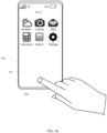
FIG. 4a is a schematic diagram of an application scenario when fingerprint recognition is performed by an electronic device according to an implementation of this application. -
FIG. 4b is a schematic diagram when fingerprint recognition is performed by a partial structure of an electronic device according to an implementation of this application. -
FIG. 5 is a flowchart of a method for preparing a laminated structure according to an implementation of this application. -
FIG. 6 is a schematic diagram of absorption axes of laminated layers of a display panel according to a second implementation of this application. -
FIG. 7 is a schematic diagram of absorption axes of laminated layers of a display panel according to a third implementation of this application. -
FIG. 8 is a schematic diagram of absorption axes of laminated layers of a display panel according to a fourth implementation of this application. -
FIG. 9 is a schematic diagram of an absorption axis of a laminated structure according to a fifth implementation of this application. -
FIG. 10 is a schematic diagram of an absorption axis of a laminated structure according to a sixth implementation of this application. -
FIG. 11 is a schematic diagram of an absorption axis of a laminated structure according to a seventh implementation of this application. -
FIG. 1 is a schematic diagram of a partial structure of an electronic device according to a first implementation. Theelectronic device 100 includes adisplay panel 101 and an opticalfingerprint recognition module 103 that are laminated. Thedisplay panel 101 is located on a light entrance side of the opticalfingerprint recognition module 103, and is configured to display an image. The opticalfingerprint recognition module 103 is configured to receive light transmitting through thedisplay panel 101 to implement a fingerprint recognition function. Theelectronic device 100 may be any electronic device such as a smartphone, a smart watch, a tablet computer, a personal digital assistant (personal digital assistant, PDA for short), a point of sales (point of sales, POS for short), an on-board computer, a desktop computer, a laptop computer, or a smart TV. This is not limited in the embodiments of the present invention. - The
display panel 101 includes alaminated structure 10 and afunctional substrate 30 that are laminated. Thefunctional substrate 30 is located between thelaminated structure 10 and the opticalfingerprint recognition module 103. Thefunctional substrate 30 has a light-transmittingarea 31, to allow light to enter the opticalfingerprint recognition module 103 through the light-transmittingarea 31. - Specifically, the
laminated structure 10 includes a quarter-wave plate (quarter-wave plate, QWP for short) 12, a linearpolarizing layer 13, and aprotective layer 15. Thefunctional substrate 30 is located between the opticalfingerprint recognition module 103 and the quarter-wave plate 12. The quarter-wave plate 12 can make ordinary light (o light) and extraordinary light (e light) equal to π/2 or an odd multiple thereof. The quarter-wave plate 12 is sandwiched between thefunctional substrate 30 and the linearpolarizing layer 13. Theprotective layer 15 is arranged on one side of the linearpolarizing layer 13 away from the quarter-wave plate 12. Both theprotective layer 15 and the linearpolarizing layer 13 can polarize light to form linearly polarized light. An angle between an absorption axis of the linearpolarizing layer 13 and an absorption axis of theprotective layer 15 is zero degrees. An angle between an absorption axis of the quarter-wave plate 12 and the absorption axis of the linearpolarizing layer 13 is 45 degrees. An angle between the absorption axis of theprotective layer 15 and the absorption axis of the quarter-wave plate 12 is 45 degrees. - In this implementation, in the linear
polarizing layer 13, light parallel to the absorption axis of the linearpolarizing layer 13 may be absorbed by the linearpolarizing layer 13, and light perpendicular to the absorption axis of the linearpolarizing layer 13 may be emitted through the linearpolarizing layer 13; and in theprotective layer 15, light parallel to the absorption axis of theprotective layer 15 may be absorbed by theprotective layer 15, and light perpendicular to the absorption axis of theprotective layer 15 may be emitted through theprotective layer 15. - Light is incident from the
protective layer 15 in a direction opposite to the linearpolarizing layer 13, becomes linearly polarized light passing through theprotective layer 15, enters the linearpolarizing layer 13, and then is converted into circularly polarized light by the quarter-wave plate 12. Part of the circularly polarized light enters the opticalfingerprint recognition module 103 through thefunctional substrate 30. - The
protective layer 15 can polarize the light incident therein to form linearly polarized light, an angle between the absorption axis of the linearpolarizing layer 13 and the absorption axis of theprotective layer 15 is zero degrees, and there is no difference between a direction of the absorption axis of theprotective layer 15 and a direction of the absorption axis of the linearpolarizing layer 13. Therefore, a luminous flux of light passing through theprotective layer 15 is roughly the same as that of light passing through the linearpolarizing layer 13. In other words, the light intensity of the light passing through theprotective layer 15 is consistent with that of the light passing through the linearpolarizing layer 13. In this way, the light loss during light transmission from thedisplay panel 10 to the opticalfingerprint recognition module 30 can be reduced, and the stability of light passing through thedisplay panel 101 can be improved, to stabilize the light intensity of the light passing through thedisplay panel 101, and improve the stability of the light entering the opticalfingerprint recognition module 103, thereby improving the recognition precision of the opticalfingerprint recognition module 103. - The
protective layer 15 is arranged on one side of thelaminated structure 10 away from the opticalfingerprint recognition module 103, namely, an outermost side of theelectronic device 100. Thelaminated structure 10 further includes a reinforcinglayer 17 arranged between theprotective layer 15 and the linearpolarizing layer 13, and used to protect other laminated structures of thelaminated structure 10 and enhance the strength of thelaminated structure 10. The reinforcinglayer 17 is a glass cover plate and can enhance the strength of thelaminated structure 10. In this implementation, the material strength of the reinforcinglayer 17 is greater than that of theprotective layer 15. Theprotective layer 15 is a film layer attached to one side of the reinforcinglayer 17 away from the linearpolarizing layer 13, for example, a protective film on the outermost side of thedisplay panel 101 of a smartphone, to prevent the reinforcinglayer 17 from being scratched and worn. - The
protective layer 15 is made of materials including polyethylene terephthalate (polyethylene terephthalate, PET for short) plastic and thermoplastic polyurethane (thermoplastic polyurethane, TUP for short) elastomer rubber. The reinforcinglayer 17 is fixed to the linearpolarizing layer 13 through an opticaladhesive layer 19. The reinforcinglayer 17 is made of an isotropic material, to reduce the light loss during light transmission in thelaminated structure 10, and enhance the stability of light transmission. The isotropic refers to a property that physical and chemical properties of an object do not change due to different directions, namely, performance values of an object measured in different directions are completely the same, and is also known as homogeneity. The opticaladhesive layer 19 is made of an isotropic material, to further reduce the light loss during light transmission in thelaminated structure 10, and enhance the stability of light transmission. It may be understood that, implementations of this application do not limit the material of theprotective layer 15 and the material of the reinforcinglayer 17. For example, the reinforcinglayer 17 may be made of plastic or ceramic. - In a possible implementation, the reinforcing
layer 17 is used to polarize light to form linearly polarized light. An angle between an absorption axis of the reinforcinglayer 17 and the absorption axis of the linearpolarizing layer 13 is zero degrees. The reinforcinglayer 17 is set as a laminated layer in a direction consistent with the direction of the absorption axis of the linear polarizing layer, so that the light intensity of light passing through theprotective layer 15 is consistent with that of light passing through the reinforcinglayer 17 and the linearpolarizing layer 13, and the optical performance of the reinforcinglayer 17, theprotective layer 15 and the linearpolarizing layer 13 can be matched, thereby enhancing the stability of light transmission in thelaminated structure 10. - In this implementation, the
display panel 101 is a flexible display panel. Thefunctional substrate 30 is an organic light-emitting diode (organic light-emitting diode, OLED for short) substrate. More specifically, thefunctional substrate 30 includes a first light-transmittinglayer 32, a plurality ofreflection units 33, and a second light-transmittinglayer 35. Thereflection units 33 are configured to reflect light irradiated thereon. Thereflection units 33 are also light-emitting units, configured to emit light. Light emitted by thereflection units 33 can be reflected by a finger and enter the opticalfingerprint recognition module 103 through the light-transmittingarea 31, thereby implementing an optical fingerprint recognition function. The plurality ofreflection units 33 are spaced on one side of the first light-transmittinglayer 32. The second light-transmittinglayer 35 covers thereflection units 33 and the first light-transmittinglayer 32. The light-transmittingarea 31 is formed between theadjacent reflection units 33. The second light-transmittinglayer 35 is located between the quarter-wave plate 12 and the first light-transmittinglayer 32. It may be understood that, thefunctional substrate 30 may also be a touch layer. - Because the
reflection units 33 are surrounded by the first light-transmittinglayer 32 and the second light-transmittinglayer 35, namely, the first light-transmittinglayer 32 and the second light-transmittinglayer 35 are arranged around thereflection units 33, an impact force on thereflection units 33 when thelaminated structure 10 is collided can be buffered, which is beneficial to prolong life of thedisplay panel 101. In this implementation, both the first light-transmittinglayer 32 and the second light-transmittinglayer 35 are made of isotropic materials, to reduce the light loss during light transmission in thedisplay panel 101, and enhance the stability of the light intensity when light passes through thedisplay panel 101. Thereflection units 33 may be a circuit part such as a cathode and an anode. - In some implementations, the
display panel 101 may be a touch display panel, and thedisplay panel 101 further includes a touch layer, arranged between thefunctional substrate 30 and the quarter-wave plate 12. - In some implementations, the
protective layer 15 only needs to meet a condition that the angle between the absorption axis of the linearpolarizing layer 13 and the absorption axis of theprotective layer 15 is zero degrees. - It may be understood that, the
laminated structure 10 includes theprotective layer 15, the linearpolarizing layer 13, and the quarter-wave plate 12 that are laminated in sequence. Theprotective layer 15 is used to polarize light to form the linearly polarized light, the angle between the absorption axis of theprotective layer 15 and the absorption axis of the linearpolarizing layer 13 is zero degrees, and the angle between the absorption axis of the linearpolarizing layer 13 and the absorption axis of the quarter-wave plate 12 is 45 degrees. -
FIG. 2 is a light path of light incident to a laminated structure in the first implementation of this application. - The light is natural light. After
light 1 is incident from one side of theprotective layer 15 away from the reinforcinglayer 17, theprotective layer 15 first polarizes the incident light to form linearlypolarized light 2. - The linearly
polarized light 2 enters the linearpolarizing layer 13 after passing through the reinforcinglayer 17 and the opticaladhesive layer 19. Because the angle between the absorption axis of the linearpolarizing layer 13 and the absorption axis of theprotective layer 15 is zero degrees, the linearlypolarized light 2 is still linearly polarized light passing through the linearpolarizing layer 13. - The linearly polarized light passing through the reinforcing
layer 17, the linearly polarized light passing through the opticaladhesive layer 19, and the linearly polarized light passing through the linearpolarizing layer 13 are marked as linearlypolarized light 3, linearlypolarized light 4, and linearlypolarized light 5 respectively. The linearlypolarized light 5 is converted into circularlypolarized light 6, for example, right circularly polarized light shown inFIG. 2 , after passing through the quarter-wave plate 12. - The circularly
polarized light 6 enters thefunctional substrate 30. Part of the circularlypolarized light 6 is reflected by thereflection units 33 of thefunctional substrate 30 and becomes reverselypolarized light 7, for example, left circularly polarized light shown inFIG. 2 . The reverselypolarized light 7 is emitted from thefunctional substrate 30 and enters the quarter-wave plate 12. The reverselypolarized light 7 is converted into linearlypolarized light 8 after passing through the quarter-wave plate 12. Obviously, a polarization angle of the linearlypolarized light 8 is rotated by 90 degrees with respect to the linearlypolarized light 5. Because the linearlypolarized light 8 is perpendicular to the absorption axis of the linearpolarizing layer 13, part of the linearlypolarized light 8 cannot pass through the linearpolarizing layer 13, thereby reducing reflected light caused by thereflection units 33 in thelaminated structure 10. Part of the circularlypolarized light 6 enters the opticalfingerprint recognition module 103 through the light-transmittingarea 31. -
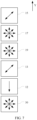
FIG. 3 is a schematic diagram of absorption axes of laminated layers of the laminated structure in the first implementation of this application. The absorption axis of theprotective layer 15 is a bidirectional absorption axis, the absorption axis of the linearpolarizing layer 13 is a bidirectional absorption axis, and the absorption axis of the quarter-wave plate 12 is a unidirectional absorption axis. An inclination angle of the absorption axis of theprotective layer 15 with respect to a first direction (for example, a Y direction shown inFIG. 3 ) is defined as N degrees. The bidirectional absorption axis means that a laminated layer (for example, theprotective layer 15 or the linear polarizing layer 13) has the same effects on light in a positive direction and a negative direction of the absorption axis. The unidirectional absorption axis means that a laminated layer (for example, the quarter-wave plate 12) has different effects on light in a direction positive and a negative direction of the absorption axis. For example, because the absorption axis of theprotective layer 15 is the bidirectional absorption axis, the light intensity of light passing through theprotective layer 15 is the same when the absorption axis of theprotective layer 15 is inclined by 45 degrees and 135 degrees with respect to the first direction. Because the absorption axis of the quarter-wave plate 12 is the unidirectional absorption axis, the light intensity of light passing through the quarter-wave plate 12 is different when the absorption axis of the quarter-wave plate 12 is inclined by 45 degrees and 135 degrees with respect to the first direction. It may be understood that, the N degrees can be any angle. An angle between the absorption axis of theprotective layer 15 and the first direction and an angle between the absorption axis of the linearpolarizing layer 13 and the first direction (for example, the Y direction shown inFIG. 3 ) are N degrees. An angle between the absorption axis of the quarter-wave plate 12 and a positive direction of the first direction is N-45 degrees. In this implementation, N is 45 degrees, that is, the absorption axis of the quarter-wave plate 12 is consistent with the positive direction of the first direction. The angle between the absorption axis of the quarter-wave plate 12 and the absorption axis of theprotective layer 15 is 45 degrees. In other words, the angle between the absorption axis of the quarter-wave plate 12 and the positive direction of the first direction is zero degrees. - An example in which the
electronic device 100 is a mobile phone is used below for description. -
FIG. 4a is a schematic diagram of an application scenario when fingerprint recognition is performed by an electronic device according to an implementation of this application.FIG. 4b is a schematic diagram when fingerprint recognition is performed by a partial structure of an electronic device according to an implementation of this application. Afinger 200 touches adisplay panel 101 to enable theelectronic device 100 to perform fingerprint recognition. Thefinger 200 is located on one side of aprotective layer 15 away from a linearpolarizing layer 13, to facilitate an opticalfingerprint recognition module 103 to perform fingerprint recognition. It may be understood that, there may also be a specific gap between thefinger 200 and theprotective layer 15, and a surface of thefinger 200 can reflect light to thedisplay panel 101. -
External light 201 is incident from theprotective layer 15 and transmitted to afunctional substrate 30 through a reinforcinglayer 17, an opticaladhesive layer 19, the linearpolarizing layer 13, and a quarter-wave plate 12. Part of theexternal light 201 is reflected byreflection units 33 into first reflectedlight 202, and part of theexternal light 201 enters the opticalfingerprint recognition module 103 through a light-transmittingarea 31. In actual application, only part of the first reflected light 202 cannot pass through the linearpolarizing layer 13 after passing through the quarter-wave plate 12, namely, is eliminated, while part of the first reflected light 202 can still be emitted from theprotective layer 15 to reach the surface of thefinger 200. The first reflected light 202 emitted from theprotective layer 15 is reflected by the surface of thefinger 200 into second reflectedlight 203. The second reflectedlight 203 enters thefunctional substrate 30 through theprotective layer 15, the reinforcinglayer 17, the opticaladhesive layer 19, the linearpolarizing layer 13, and the quarter-wave plate 12, and is incident to the opticalfingerprint recognition module 103 through the light-transmittingarea 31 of thefunctional substrate 30. - The
reflection units 33 emitlight 204. The light 204 is emitted to the surface of thefinger 200 through the quarter-wave plate 12, the linearpolarizing layer 13, the opticaladhesive layer 19, the reinforcinglayer 17, and theprotective layer 15. The light 204 is reflected by the surface of thefinger 200 into third reflectedlight 205. The third reflected light 205 then enters the opticalfingerprint recognition module 103 through theprotective layer 15, the reinforcinglayer 17, the opticaladhesive layer 19, the linearpolarizing layer 13, the quarter-wave plate 12, and the light-transmittingarea 31 of thefunctional substrate 30. The opticalfingerprint recognition module 103 performs fingerprint recognition. - An angle between an absorption axis of the
protective layer 15 and an absorption axis of the linearpolarizing layer 13 is zero degrees, and a luminous flux of the reflected light (for example, the second reflected light 203 or the third reflected light 205) reflected from the surface of thefinger 200 after passing through theprotective layer 15 is roughly the same as that after passing through the linearpolarizing layer 13. In other words, the light intensity of light passing through theprotective layer 15 is consistent with that of light passing through the linearpolarizing layer 13, to stabilize the light intensity of light passing through thedisplay panel 101, and improve the stability of the light passing through thedisplay panel 101, thereby improving the recognition precision of the opticalfingerprint recognition module 103. -
FIG. 5 a flowchart of a method for preparing a laminated structure according to an implementation of this application. The method for preparing a laminated structure includes the following steps: - Step 501: Provide a quarter-wave plate, a linear polarizing layer and a protective layer.
- Step 502: Attach the linear polarizing layer to the quarter-wave plate, and arrange the protective layer on one side of the linear polarizing layer away from the quarter-wave plate, so that the protective layer, the linear polarizing layer and the quarter-wave plate are laminated, where the protective layer is used to polarize light to form linearly polarized light, an angle between an absorption axis of the protective layer and an absorption axis of the linear polarizing layer is zero degrees, and an angle between the absorption axis of the linear polarizing layer and an absorption axis of the quarter-wave plate is 45 degrees.
- In an implementation, the arranging the protective layer on one side of the linear polarizing layer away from the quarter-wave plate includes: arranging a reinforcing layer on one side of the linear polarizing layer away from the quarter-wave plate, and arranging the protective layer on one side of the reinforcing layer away from the linear polarizing layer.
- In another implementation, the arranging a reinforcing layer on one side of the linear polarizing layer away from the quarter-wave plate includes: fixing the reinforcing layer on the linear polarizing layer through an optical adhesive layer.
-
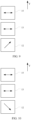
FIG. 6 is a schematic diagram of absorption axes of laminated layers of a display panel according to a second implementation of this application. The display panel provided in the second implementation is roughly the same as the display panel provided in the first implementation, except that an angle between an absorption axis of a quarter-wave plate 12 and a positive direction of a first direction is N+45 degrees, where N is 45 degrees. In this case, the angle between the absorption axis of the quarter-wave plate 12 and the positive direction of the first direction is 90 degrees, and an angle between an absorption axis of aprotective layer 15 and the absorption axis of the quarter-wave plate 12 is 45 degrees. - The
protective layer 15 can polarize light incident therein to form linearly polarized light, an angle between an absorption axis of a linearpolarizing layer 13 and the absorption axis of theprotective layer 15 is zero degrees, and there is no difference between a direction of the absorption axis of theprotective layer 15 and a direction of the absorption axis of the linearpolarizing layer 13. Therefore, a luminous flux of light passing through theprotective layer 15 is roughly the same as that of light passing through the linearpolarizing layer 13. In other words, the light intensity of the light passing through theprotective layer 15 is consistent with that of the light passing through the linearpolarizing layer 13, and the stability of light passing through the display panel is improved, to stabilize the light intensity of the light passing through the display panel, and improve the stability of light entering an optical fingerprint recognition module, thereby improving the recognition precision of the optical fingerprint recognition module. -
FIG. 7 is a schematic diagram of absorption axes of laminated layers of a display panel according to a third implementation of this application. The display panel provided in the third implementation is roughly the same as the display panel provided in the first implementation, except that an angle between an absorption axis of a quarter-wave plate 12 and a positive direction of a first direction is N+3×45 degrees, where N is 45 degrees. In this case, the angle between the absorption axis of the quarter-wave plate 12 and the positive direction of the first direction is 180 degrees, and an angle between an absorption axis of aprotective layer 15 and the absorption axis of the quarter-wave plate 12 is 45 degrees. -
FIG. 8 is a schematic diagram of absorption axes of laminated layers of a display panel according to the fourth implementation of this application. The display panel provided in the fourth implementation is roughly the same as the display panel provided in the first implementation, except that an angle between an absorption axis of a quarter-wave plate 12 and a positive direction of a first direction is N+5×45 degrees, where N is 45 degrees. In this case, the angle between the absorption axis of the quarter-wave plate 12 and the positive direction of the first direction is 270 degrees, and an angle between an absorption axis of aprotective layer 15 and the absorption axis of the quarter-wave plate 12 is 45 degrees. -
FIG. 9 is a schematic diagram of an absorption axis of a laminated structure according to a fifth implementation of this application. A laminated structure of a display panel provided in the fifth implementation is roughly the same as that of the display panel provided in the first implementation, except that an inclination angle of an absorption axis of aprotective layer 15 with respect to a first direction (for example, a Y direction shown inFIG. 9 ) is 90 degrees, namely, N is 90 degrees, an inclination angle of an absorption axis of a linearpolarizing layer 13 with respect to the first direction (for example, the Y direction shown inFIG. 9 ) is 90 degrees, and an angle between an absorption axis of a quarter-wave plate 12 and a positive direction of the first direction is N-45 degrees. In this case, the angle between the absorption axis of the quarter-wave plate 12 and the positive direction of the first direction is 45 degrees, and an angle between the absorption axis of theprotective layer 15 and the absorption axis of the quarter-wave plate 12 is 45 degrees. -
FIG. 10 is a schematic diagram of an absorption axis of a laminated structure according to a sixth implementation of this application. A laminated structure of a display panel provided in the sixth implementation is roughly the same as that of the display panel provided in the first implementation, except that an inclination angle of an absorption axis of aprotective layer 15 with respect to a first direction (for example, a Y direction shown inFIG. 10 ) is 90 degrees, namely, N is 90 degrees, an inclination angle of an absorption axis of a linearpolarizing layer 13 with respect to the first direction (for example, the Y direction shown inFIG. 10 ) is 90 degrees, and an angle between an absorption axis of a quarter-wave plate 12 and a positive direction of the first direction is N+45 degrees. In this case, the angle between the absorption axis of the quarter-wave plate 12 and the positive direction of the first direction is 135 degrees, and an angle between the absorption axis of theprotective layer 15 and the absorption axis of the quarter-wave plate 12 is 45 degrees. -
FIG. 11 is a schematic diagram of an absorption axis of a laminated structure according to a seventh implementation of this application. A laminated structure of a display panel provided in the seventh implementation is roughly the same as that of the display panel provided in the first implementation, except that an inclination angle of an absorption axis of aprotective layer 15 with respect to a first direction (for example, a Y direction shown inFIG. 11 ) is 90 degrees, namely, N is 90 degrees, an inclination angle of an absorption axis of a linearpolarizing layer 13 with respect to the first direction (for example, the Y direction shown inFIG. 11 ) is 90 degrees, and an angle between an absorption axis of a quarter-wave plate 12 and a positive direction of the first direction is N+3 ×45 degrees. In this case, the angle between the absorption axis of the quarter-wave plate 12 and the positive direction of the first direction is 225 degrees (also 135 degrees), and an angle between the absorption axis of theprotective layer 15 and the absorption axis of the quarter-wave plate 12 is 45 degrees. - The foregoing descriptions are merely specific implementations of the present invention, but are not intended to limit the protection scope of the present invention. Any variation or replacement readily figured out by a person skilled in the art within the technical scope disclosed in the present invention shall fall within the protection scope of the present invention Therefore, the protection scope of the present invention shall be subject to the protection scope of the claims.
Claims (11)
- A laminated structure, wherein the laminated structure comprises a protective layer, a linear polarizing layer, and a quarter-wave plate that are laminated in sequence, the protective layer is used to polarize light to form linearly polarized light, an angle between an absorption axis of the protective layer and an absorption axis of the linear polarizing layer is zero degrees, and an angle between the absorption axis of the linear polarizing layer and an absorption axis of the quarter-wave plate is 45 degrees.
- The laminated structure according to claim 1, wherein the laminated structure further comprises a reinforcing layer arranged between the protective layer and the linear polarizing layer.
- The laminated structure according to claim 2, wherein the reinforcing layer is made of an isotropic material.
- The laminated structure according to claim 3, wherein the reinforcing layer is a glass cover plate.
- The laminated structure according to claim 2, wherein the linear polarizing layer is fixed to the reinforcing layer through an optical adhesive layer.
- The laminated structure according to claim 5, wherein the optical adhesive layer is made of an isotropic material.
- The laminated structure according to claim 2, wherein the reinforcing layer is used to polarize light to form linearly polarized light, and an angle between an absorption axis of the reinforcing layer and the absorption axis of the linear polarizing layer is zero degrees.
- A display panel, applied to an electronic device with an optical fingerprint recognition module, wherein the display panel comprises the laminated structure according to any one of claims 1 to 7 and a functional substrate, the functional substrate is located on one side of the quarter-wave plate away from the protective layer, and the functional substrate has a light-transmitting area, to allow light emitted from the quarter-wave plate to enter the optical fingerprint recognition module through the light-transmitting area.
- The display panel according to claim 8, wherein the functional substrate comprises a first light-transmitting layer, a plurality of reflection units, and a second light-transmitting layer, the plurality of reflection units are spaced on the first light-transmitting layer, the second light-transmitting layer covers the reflection units and the first light-transmitting layer, the light-transmitting area is formed between the adjacent reflection units, and the second light-transmitting layer is located between the quarter-wave plate and the first light-transmitting layer.
- The display panel according to claim 9, wherein both the first light-transmitting layer and the second light-transmitting layer are made of isotropic materials.
- An electronic device, comprising the display panel according to any one of claims 8 to 10 and an optical fingerprint recognition module, wherein the optical fingerprint recognition module is located on one side of a functional substrate away from the protective layer, and is configured to receive light passing through a light-transmitting area of the functional substrate.
Applications Claiming Priority (3)
| Application Number | Priority Date | Filing Date | Title |
|---|---|---|---|
| CN201910415213.3A CN111950335B (en) | 2019-05-17 | 2019-05-17 | Laminated structure, display panel and electronic device |
| PCT/CN2020/090531 WO2020233521A1 (en) | 2019-05-17 | 2020-05-15 | Laminated structure, display panel and electronic device |
| EP20810180.8A EP3964887B1 (en) | 2019-05-17 | 2020-05-15 | Laminated structure, display panel and electronic device |
Related Parent Applications (2)
| Application Number | Title | Priority Date | Filing Date |
|---|---|---|---|
| EP20810180.8A Division-Into EP3964887B1 (en) | 2019-05-17 | 2020-05-15 | Laminated structure, display panel and electronic device |
| EP20810180.8A Division EP3964887B1 (en) | 2019-05-17 | 2020-05-15 | Laminated structure, display panel and electronic device |
Publications (3)
| Publication Number | Publication Date |
|---|---|
| EP4246469A2 true EP4246469A2 (en) | 2023-09-20 |
| EP4246469A3 EP4246469A3 (en) | 2023-11-15 |
| EP4246469B1 EP4246469B1 (en) | 2024-10-16 |
Family
ID=73336914
Family Applications (2)
| Application Number | Title | Priority Date | Filing Date |
|---|---|---|---|
| EP23170685.4A Active EP4246469B1 (en) | 2019-05-17 | 2020-05-15 | Laminated structure, display panel and electronic device |
| EP20810180.8A Active EP3964887B1 (en) | 2019-05-17 | 2020-05-15 | Laminated structure, display panel and electronic device |
Family Applications After (1)
| Application Number | Title | Priority Date | Filing Date |
|---|---|---|---|
| EP20810180.8A Active EP3964887B1 (en) | 2019-05-17 | 2020-05-15 | Laminated structure, display panel and electronic device |
Country Status (4)
| Country | Link |
|---|---|
| US (1) | US12340616B2 (en) |
| EP (2) | EP4246469B1 (en) |
| CN (1) | CN111950335B (en) |
| WO (1) | WO2020233521A1 (en) |
Families Citing this family (1)
| Publication number | Priority date | Publication date | Assignee | Title |
|---|---|---|---|---|
| CN115274812B (en) * | 2022-08-19 | 2025-08-19 | 京东方科技集团股份有限公司 | Display panel, preparation method thereof and display device |
Family Cites Families (33)
| Publication number | Priority date | Publication date | Assignee | Title |
|---|---|---|---|---|
| JP3748406B2 (en) * | 2001-12-18 | 2006-02-22 | 株式会社日立製作所 | Display device |
| JP3851919B2 (en) * | 2004-12-20 | 2006-11-29 | 日東電工株式会社 | Liquid crystal panel and liquid crystal display device |
| JP2007310260A (en) | 2006-05-22 | 2007-11-29 | Konica Minolta Opto Inc | Polarizing plate protective film and polarizing plate |
| US8180120B2 (en) * | 2007-03-09 | 2012-05-15 | Authentec, Inc. | Finger sensor using polarized light and associated methods |
| EP2437106B1 (en) | 2009-05-27 | 2020-11-18 | Sharp Kabushiki Kaisha | Liquid crystal display device |
| CN202693957U (en) * | 2012-07-02 | 2013-01-23 | 天马微电子股份有限公司 | Liquid crystal display panel and liquid crystal display device |
| KR101628428B1 (en) | 2012-12-17 | 2016-06-08 | 제일모직주식회사 | Polarizing plate, method for preparing the same and optical display apparatus comprising the same |
| CN103207426B (en) * | 2013-03-28 | 2015-09-16 | 京东方科技集团股份有限公司 | A kind of polaroid and display device |
| KR101735689B1 (en) | 2014-02-21 | 2017-05-15 | 주식회사 엘지화학 | Circulary polarizing plate, and touch panel and display device comprising the same |
| CN104062802A (en) * | 2014-07-15 | 2014-09-24 | 深圳市华星光电技术有限公司 | Round polaroid, liquid crystal display panel and liquid crystal display device |
| JP6081429B2 (en) | 2014-10-16 | 2017-02-15 | 日東電工株式会社 | Polarizing plate and liquid crystal display device |
| CN107750343B (en) | 2015-06-15 | 2021-03-05 | 3M创新有限公司 | Optical stack including reflective-absorptive polarizer |
| CN107203732A (en) * | 2016-03-16 | 2017-09-26 | 上海箩箕技术有限公司 | Optical fingerprint sensor module |
| CN105843452B (en) * | 2016-05-13 | 2019-11-01 | 中航华东光电有限公司 | A kind of low reflection OLED display of integrated resistor touch function |
| CN105954917A (en) * | 2016-06-29 | 2016-09-21 | 京东方科技集团股份有限公司 | Display apparatus |
| CN106772720A (en) * | 2016-12-06 | 2017-05-31 | 四川龙华光电薄膜股份有限公司 | Visual angle margining tablet and its manufacture method |
| CN106710449A (en) * | 2016-12-09 | 2017-05-24 | 京东方科技集团股份有限公司 | Flexible display module and display device |
| CN107024551A (en) | 2017-03-28 | 2017-08-08 | 山东省药学科学院 | The concentration detection method of dextrorotation thunder shellfish and its metabolite in a kind of dog plasma |
| CN107025451B (en) * | 2017-04-27 | 2019-11-08 | 上海天马微电子有限公司 | A display panel and a display device |
| CN107230698B (en) * | 2017-05-27 | 2019-09-03 | 上海天马微电子有限公司 | Display panel and display device |
| CN107133613B (en) * | 2017-06-06 | 2020-06-30 | 上海天马微电子有限公司 | A display panel and display device |
| CN107065274B (en) * | 2017-06-19 | 2020-03-10 | 上海天马微电子有限公司 | Array substrate, display panel and display device |
| CN107340561B (en) * | 2017-09-04 | 2020-07-21 | 深圳Tcl新技术有限公司 | Polarizing plate and liquid crystal display |
| TWI844520B (en) * | 2017-10-10 | 2024-06-11 | 美商康寧公司 | Vehicle interior systems having a curved cover glass with improved reliability and methods for forming the same |
| CN107728844A (en) * | 2017-10-18 | 2018-02-23 | 武汉华星光电半导体显示技术有限公司 | A kind of cover plate and display device of integrated polaroid and touch controllable function |
| TWI840337B (en) * | 2017-11-30 | 2024-05-01 | 日商半導體能源研究所股份有限公司 | Display panel, display device, display module, electronic device, and manufacturing method of display panel |
| KR101912124B1 (en) * | 2017-12-11 | 2018-10-29 | (주)유티아이 | optical filter cell array structure and manufacturing method of optical filter cell array structure thereby |
| CN107884982B (en) * | 2017-12-27 | 2020-06-05 | 惠州市华星光电技术有限公司 | Liquid crystal display screen |
| KR101938413B1 (en) | 2018-06-05 | 2019-01-14 | 동우 화인켐 주식회사 | Optical film and flexible display device including the same |
| EP3627385B1 (en) | 2018-08-06 | 2023-07-05 | Shenzhen Goodix Technology Co., Ltd. | Under-screen optical fingerprint identification device and electronic device |
| CN109036162B (en) * | 2018-08-29 | 2021-06-29 | 上海天马有机发光显示技术有限公司 | An organic light-emitting display panel, a preparation method and a display device |
| CN109190599A (en) * | 2018-10-15 | 2019-01-11 | 武汉华星光电半导体显示技术有限公司 | A kind of display panel |
| CN111626195B (en) * | 2020-05-26 | 2024-04-12 | 京东方科技集团股份有限公司 | Display device, signal identification method thereof and lock body |
-
2019
- 2019-05-17 CN CN201910415213.3A patent/CN111950335B/en active Active
-
2020
- 2020-05-15 US US17/611,274 patent/US12340616B2/en active Active
- 2020-05-15 EP EP23170685.4A patent/EP4246469B1/en active Active
- 2020-05-15 WO PCT/CN2020/090531 patent/WO2020233521A1/en not_active Ceased
- 2020-05-15 EP EP20810180.8A patent/EP3964887B1/en active Active
Also Published As
| Publication number | Publication date |
|---|---|
| WO2020233521A1 (en) | 2020-11-26 |
| EP3964887B1 (en) | 2023-06-21 |
| US20220236469A1 (en) | 2022-07-28 |
| EP3964887A4 (en) | 2022-05-18 |
| US12340616B2 (en) | 2025-06-24 |
| EP3964887A1 (en) | 2022-03-09 |
| CN111950335A (en) | 2020-11-17 |
| CN111950335B (en) | 2023-07-21 |
| EP4246469B1 (en) | 2024-10-16 |
| EP4246469A3 (en) | 2023-11-15 |
Similar Documents
| Publication | Publication Date | Title |
|---|---|---|
| KR102170023B1 (en) | Flexible display panel, manufacturing method thereof, and flexible display device | |
| CN101523275B (en) | Display device | |
| US7589798B2 (en) | Touch panel having upper electrode plate including electrode, polarizing plate, quarter wave plate and heat-resistant transparent resin plate | |
| US9818017B2 (en) | Fingerprint identification module | |
| US11450139B2 (en) | Protective film for OLED display with fingerprint recognition system | |
| KR20200030663A (en) | Flexible window and flexible display device comprising the same | |
| JP2020034916A (en) | Foldable display | |
| US9535548B2 (en) | Display device | |
| KR20160063964A (en) | flexible display device | |
| KR20140090366A (en) | Window member, method of fabricating the same and dispaly device having the same | |
| WO2019158065A1 (en) | Protective film and method and device for cutting protective film | |
| KR20230050499A (en) | Display device | |
| EP3196691A1 (en) | Liquid crystal display device | |
| KR20220019898A (en) | Electronic device | |
| CN113939751B (en) | Optical laminate | |
| KR20250052322A (en) | A protection film and a display device including the same | |
| CN109036162B (en) | An organic light-emitting display panel, a preparation method and a display device | |
| CN106918859B (en) | Polarizing film and display device having polarizing film | |
| EP4246469B1 (en) | Laminated structure, display panel and electronic device | |
| CN115707292A (en) | Display device and providing method thereof | |
| US11997868B2 (en) | Display device including buffer filled indented glass region | |
| US11281041B2 (en) | Cover glass structure and display apparatus comprising thereof | |
| KR102810393B1 (en) | Display device | |
| HK40068847A (en) | Laminated structure, display panel and electronic device | |
| HK40068847B (en) | Laminated structure, display panel and electronic device |
Legal Events
| Date | Code | Title | Description |
|---|---|---|---|
| PUAI | Public reference made under article 153(3) epc to a published international application that has entered the european phase |
Free format text: ORIGINAL CODE: 0009012 |
|
| STAA | Information on the status of an ep patent application or granted ep patent |
Free format text: STATUS: REQUEST FOR EXAMINATION WAS MADE |
|
| 17P | Request for examination filed |
Effective date: 20230428 |
|
| AC | Divisional application: reference to earlier application |
Ref document number: 3964887 Country of ref document: EP Kind code of ref document: P |
|
| AK | Designated contracting states |
Kind code of ref document: A2 Designated state(s): AL AT BE BG CH CY CZ DE DK EE ES FI FR GB GR HR HU IE IS IT LI LT LU LV MC MK MT NL NO PL PT RO RS SE SI SK SM TR |
|
| REG | Reference to a national code |
Ref legal event code: R079 Free format text: PREVIOUS MAIN CLASS: G06V0040130000 Ref country code: DE Ref legal event code: R079 Ref document number: 602020039757 Country of ref document: DE Free format text: PREVIOUS MAIN CLASS: G06V0040130000 Ipc: G02B0005300000 |
|
| PUAL | Search report despatched |
Free format text: ORIGINAL CODE: 0009013 |
|
| AK | Designated contracting states |
Kind code of ref document: A3 Designated state(s): AL AT BE BG CH CY CZ DE DK EE ES FI FR GB GR HR HU IE IS IT LI LT LU LV MC MK MT NL NO PL PT RO RS SE SI SK SM TR |
|
| RIC1 | Information provided on ipc code assigned before grant |
Ipc: G02B 1/14 20150101ALI20231012BHEP Ipc: G06V 40/13 20220101ALI20231012BHEP Ipc: G02F 1/1335 20060101ALI20231012BHEP Ipc: G02B 5/30 20060101AFI20231012BHEP |
|
| GRAP | Despatch of communication of intention to grant a patent |
Free format text: ORIGINAL CODE: EPIDOSNIGR1 |
|
| STAA | Information on the status of an ep patent application or granted ep patent |
Free format text: STATUS: GRANT OF PATENT IS INTENDED |
|
| RIC1 | Information provided on ipc code assigned before grant |
Ipc: G02B 1/14 20150101ALI20240422BHEP Ipc: G06V 40/13 20220101ALI20240422BHEP Ipc: G02F 1/1335 20060101ALI20240422BHEP Ipc: G02B 5/30 20060101AFI20240422BHEP |
|
| INTG | Intention to grant announced |
Effective date: 20240517 |
|
| GRAS | Grant fee paid |
Free format text: ORIGINAL CODE: EPIDOSNIGR3 |
|
| GRAA | (expected) grant |
Free format text: ORIGINAL CODE: 0009210 |
|
| STAA | Information on the status of an ep patent application or granted ep patent |
Free format text: STATUS: THE PATENT HAS BEEN GRANTED |
|
| AC | Divisional application: reference to earlier application |
Ref document number: 3964887 Country of ref document: EP Kind code of ref document: P |
|
| AK | Designated contracting states |
Kind code of ref document: B1 Designated state(s): AL AT BE BG CH CY CZ DE DK EE ES FI FR GB GR HR HU IE IS IT LI LT LU LV MC MK MT NL NO PL PT RO RS SE SI SK SM TR |
|
| REG | Reference to a national code |
Ref country code: GB Ref legal event code: FG4D |
|
| REG | Reference to a national code |
Ref country code: CH Ref legal event code: EP |
|
| REG | Reference to a national code |
Ref country code: IE Ref legal event code: FG4D |
|
| REG | Reference to a national code |
Ref country code: DE Ref legal event code: R096 Ref document number: 602020039757 Country of ref document: DE |
|
| REG | Reference to a national code |
Ref country code: NL Ref legal event code: FP |
|
| REG | Reference to a national code |
Ref country code: LT Ref legal event code: MG9D |
|
| REG | Reference to a national code |
Ref country code: AT Ref legal event code: MK05 Ref document number: 1733360 Country of ref document: AT Kind code of ref document: T Effective date: 20241016 |
|
| PG25 | Lapsed in a contracting state [announced via postgrant information from national office to epo] |
Ref country code: IS Free format text: LAPSE BECAUSE OF FAILURE TO SUBMIT A TRANSLATION OF THE DESCRIPTION OR TO PAY THE FEE WITHIN THE PRESCRIBED TIME-LIMIT Effective date: 20250216 Ref country code: HR Free format text: LAPSE BECAUSE OF FAILURE TO SUBMIT A TRANSLATION OF THE DESCRIPTION OR TO PAY THE FEE WITHIN THE PRESCRIBED TIME-LIMIT Effective date: 20241016 Ref country code: PT Free format text: LAPSE BECAUSE OF FAILURE TO SUBMIT A TRANSLATION OF THE DESCRIPTION OR TO PAY THE FEE WITHIN THE PRESCRIBED TIME-LIMIT Effective date: 20250217 |
|
| PG25 | Lapsed in a contracting state [announced via postgrant information from national office to epo] |
Ref country code: FI Free format text: LAPSE BECAUSE OF FAILURE TO SUBMIT A TRANSLATION OF THE DESCRIPTION OR TO PAY THE FEE WITHIN THE PRESCRIBED TIME-LIMIT Effective date: 20241016 |
|
| PG25 | Lapsed in a contracting state [announced via postgrant information from national office to epo] |
Ref country code: BG Free format text: LAPSE BECAUSE OF FAILURE TO SUBMIT A TRANSLATION OF THE DESCRIPTION OR TO PAY THE FEE WITHIN THE PRESCRIBED TIME-LIMIT Effective date: 20241016 |
|
| PG25 | Lapsed in a contracting state [announced via postgrant information from national office to epo] |
Ref country code: ES Free format text: LAPSE BECAUSE OF FAILURE TO SUBMIT A TRANSLATION OF THE DESCRIPTION OR TO PAY THE FEE WITHIN THE PRESCRIBED TIME-LIMIT Effective date: 20241016 |
|
| PG25 | Lapsed in a contracting state [announced via postgrant information from national office to epo] |
Ref country code: NO Free format text: LAPSE BECAUSE OF FAILURE TO SUBMIT A TRANSLATION OF THE DESCRIPTION OR TO PAY THE FEE WITHIN THE PRESCRIBED TIME-LIMIT Effective date: 20250116 |
|
| PG25 | Lapsed in a contracting state [announced via postgrant information from national office to epo] |
Ref country code: LV Free format text: LAPSE BECAUSE OF FAILURE TO SUBMIT A TRANSLATION OF THE DESCRIPTION OR TO PAY THE FEE WITHIN THE PRESCRIBED TIME-LIMIT Effective date: 20241016 Ref country code: AT Free format text: LAPSE BECAUSE OF FAILURE TO SUBMIT A TRANSLATION OF THE DESCRIPTION OR TO PAY THE FEE WITHIN THE PRESCRIBED TIME-LIMIT Effective date: 20241016 Ref country code: GR Free format text: LAPSE BECAUSE OF FAILURE TO SUBMIT A TRANSLATION OF THE DESCRIPTION OR TO PAY THE FEE WITHIN THE PRESCRIBED TIME-LIMIT Effective date: 20250117 |
|
| PG25 | Lapsed in a contracting state [announced via postgrant information from national office to epo] |
Ref country code: PL Free format text: LAPSE BECAUSE OF FAILURE TO SUBMIT A TRANSLATION OF THE DESCRIPTION OR TO PAY THE FEE WITHIN THE PRESCRIBED TIME-LIMIT Effective date: 20241016 |
|
| PG25 | Lapsed in a contracting state [announced via postgrant information from national office to epo] |
Ref country code: RS Free format text: LAPSE BECAUSE OF FAILURE TO SUBMIT A TRANSLATION OF THE DESCRIPTION OR TO PAY THE FEE WITHIN THE PRESCRIBED TIME-LIMIT Effective date: 20250116 |
|
| PGFP | Annual fee paid to national office [announced via postgrant information from national office to epo] |
Ref country code: NL Payment date: 20250409 Year of fee payment: 6 |
|
| PG25 | Lapsed in a contracting state [announced via postgrant information from national office to epo] |
Ref country code: SM Free format text: LAPSE BECAUSE OF FAILURE TO SUBMIT A TRANSLATION OF THE DESCRIPTION OR TO PAY THE FEE WITHIN THE PRESCRIBED TIME-LIMIT Effective date: 20241016 |
|
| PGFP | Annual fee paid to national office [announced via postgrant information from national office to epo] |
Ref country code: DE Payment date: 20250402 Year of fee payment: 6 |
|
| PG25 | Lapsed in a contracting state [announced via postgrant information from national office to epo] |
Ref country code: DK Free format text: LAPSE BECAUSE OF FAILURE TO SUBMIT A TRANSLATION OF THE DESCRIPTION OR TO PAY THE FEE WITHIN THE PRESCRIBED TIME-LIMIT Effective date: 20241016 |
|
| REG | Reference to a national code |
Ref country code: DE Ref legal event code: R097 Ref document number: 602020039757 Country of ref document: DE |
|
| PG25 | Lapsed in a contracting state [announced via postgrant information from national office to epo] |
Ref country code: EE Free format text: LAPSE BECAUSE OF FAILURE TO SUBMIT A TRANSLATION OF THE DESCRIPTION OR TO PAY THE FEE WITHIN THE PRESCRIBED TIME-LIMIT Effective date: 20241016 |
|
| PG25 | Lapsed in a contracting state [announced via postgrant information from national office to epo] |
Ref country code: RO Free format text: LAPSE BECAUSE OF FAILURE TO SUBMIT A TRANSLATION OF THE DESCRIPTION OR TO PAY THE FEE WITHIN THE PRESCRIBED TIME-LIMIT Effective date: 20241016 |
|
| PG25 | Lapsed in a contracting state [announced via postgrant information from national office to epo] |
Ref country code: SK Free format text: LAPSE BECAUSE OF FAILURE TO SUBMIT A TRANSLATION OF THE DESCRIPTION OR TO PAY THE FEE WITHIN THE PRESCRIBED TIME-LIMIT Effective date: 20241016 |
|
| PG25 | Lapsed in a contracting state [announced via postgrant information from national office to epo] |
Ref country code: CZ Free format text: LAPSE BECAUSE OF FAILURE TO SUBMIT A TRANSLATION OF THE DESCRIPTION OR TO PAY THE FEE WITHIN THE PRESCRIBED TIME-LIMIT Effective date: 20241016 |
|
| PG25 | Lapsed in a contracting state [announced via postgrant information from national office to epo] |
Ref country code: IT Free format text: LAPSE BECAUSE OF FAILURE TO SUBMIT A TRANSLATION OF THE DESCRIPTION OR TO PAY THE FEE WITHIN THE PRESCRIBED TIME-LIMIT Effective date: 20241016 |
|
| PLBE | No opposition filed within time limit |
Free format text: ORIGINAL CODE: 0009261 |
|
| STAA | Information on the status of an ep patent application or granted ep patent |
Free format text: STATUS: NO OPPOSITION FILED WITHIN TIME LIMIT |
|
| PG25 | Lapsed in a contracting state [announced via postgrant information from national office to epo] |
Ref country code: SE Free format text: LAPSE BECAUSE OF FAILURE TO SUBMIT A TRANSLATION OF THE DESCRIPTION OR TO PAY THE FEE WITHIN THE PRESCRIBED TIME-LIMIT Effective date: 20241016 |
|
| 26N | No opposition filed |
Effective date: 20250717 |
|
| REG | Reference to a national code |
Ref country code: CH Ref legal event code: H13 Free format text: ST27 STATUS EVENT CODE: U-0-0-H10-H13 (AS PROVIDED BY THE NATIONAL OFFICE) Effective date: 20251223 |
|
| PG25 | Lapsed in a contracting state [announced via postgrant information from national office to epo] |
Ref country code: LU Free format text: LAPSE BECAUSE OF NON-PAYMENT OF DUE FEES Effective date: 20250515 |
|
| PG25 | Lapsed in a contracting state [announced via postgrant information from national office to epo] |
Ref country code: CH Free format text: LAPSE BECAUSE OF NON-PAYMENT OF DUE FEES Effective date: 20250531 |
|
| REG | Reference to a national code |
Ref country code: BE Ref legal event code: MM Effective date: 20250531 |
|
| PG25 | Lapsed in a contracting state [announced via postgrant information from national office to epo] |
Ref country code: MC Free format text: LAPSE BECAUSE OF FAILURE TO SUBMIT A TRANSLATION OF THE DESCRIPTION OR TO PAY THE FEE WITHIN THE PRESCRIBED TIME-LIMIT Effective date: 20241016 |
|
| PGFP | Annual fee paid to national office [announced via postgrant information from national office to epo] |
Ref country code: GB Payment date: 20260324 Year of fee payment: 7 |
|
| PG25 | Lapsed in a contracting state [announced via postgrant information from national office to epo] |
Ref country code: IE Free format text: LAPSE BECAUSE OF NON-PAYMENT OF DUE FEES Effective date: 20250515 |
|
| PG25 | Lapsed in a contracting state [announced via postgrant information from national office to epo] |
Ref country code: BE Free format text: LAPSE BECAUSE OF NON-PAYMENT OF DUE FEES Effective date: 20250531 |
|
| PG25 | Lapsed in a contracting state [announced via postgrant information from national office to epo] |
Ref country code: FR Free format text: LAPSE BECAUSE OF NON-PAYMENT OF DUE FEES Effective date: 20250531 |