EP4246179A1 - Ultrasound transmitter device for driving piezoelectric transducers - Google Patents
Ultrasound transmitter device for driving piezoelectric transducers Download PDFInfo
- Publication number
- EP4246179A1 EP4246179A1 EP23158628.0A EP23158628A EP4246179A1 EP 4246179 A1 EP4246179 A1 EP 4246179A1 EP 23158628 A EP23158628 A EP 23158628A EP 4246179 A1 EP4246179 A1 EP 4246179A1
- Authority
- EP
- European Patent Office
- Prior art keywords
- coupled
- current
- transistors
- value
- central
- Prior art date
- Legal status (The legal status is an assumption and is not a legal conclusion. Google has not performed a legal analysis and makes no representation as to the accuracy of the status listed.)
- Withdrawn
Links
Images


Classifications
-
- G—PHYSICS
- G01—MEASURING; TESTING
- G01S—RADIO DIRECTION-FINDING; RADIO NAVIGATION; DETERMINING DISTANCE OR VELOCITY BY USE OF RADIO WAVES; LOCATING OR PRESENCE-DETECTING BY USE OF THE REFLECTION OR RERADIATION OF RADIO WAVES; ANALOGOUS ARRANGEMENTS USING OTHER WAVES
- G01S15/00—Systems using the reflection or reradiation of acoustic waves, e.g. sonar systems
- G01S15/02—Systems using the reflection or reradiation of acoustic waves, e.g. sonar systems using reflection of acoustic waves
- G01S15/06—Systems determining the position data of a target
- G01S15/08—Systems for measuring distance only
- G01S15/10—Systems for measuring distance only using transmission of interrupted, pulse-modulated waves
- G01S15/102—Systems for measuring distance only using transmission of interrupted, pulse-modulated waves using transmission of pulses having some particular characteristics
-
- B—PERFORMING OPERATIONS; TRANSPORTING
- B06—GENERATING OR TRANSMITTING MECHANICAL VIBRATIONS IN GENERAL
- B06B—METHODS OR APPARATUS FOR GENERATING OR TRANSMITTING MECHANICAL VIBRATIONS OF INFRASONIC, SONIC, OR ULTRASONIC FREQUENCY, e.g. FOR PERFORMING MECHANICAL WORK IN GENERAL
- B06B1/00—Methods or apparatus for generating mechanical vibrations of infrasonic, sonic, or ultrasonic frequency
- B06B1/02—Methods or apparatus for generating mechanical vibrations of infrasonic, sonic, or ultrasonic frequency making use of electrical energy
- B06B1/0207—Driving circuits
- B06B1/0215—Driving circuits for generating pulses, e.g. bursts of oscillations, envelopes
-
- B—PERFORMING OPERATIONS; TRANSPORTING
- B06—GENERATING OR TRANSMITTING MECHANICAL VIBRATIONS IN GENERAL
- B06B—METHODS OR APPARATUS FOR GENERATING OR TRANSMITTING MECHANICAL VIBRATIONS OF INFRASONIC, SONIC, OR ULTRASONIC FREQUENCY, e.g. FOR PERFORMING MECHANICAL WORK IN GENERAL
- B06B1/00—Methods or apparatus for generating mechanical vibrations of infrasonic, sonic, or ultrasonic frequency
- B06B1/02—Methods or apparatus for generating mechanical vibrations of infrasonic, sonic, or ultrasonic frequency making use of electrical energy
- B06B1/06—Methods or apparatus for generating mechanical vibrations of infrasonic, sonic, or ultrasonic frequency making use of electrical energy operating with piezoelectric effect or with electrostriction
-
- G—PHYSICS
- G01—MEASURING; TESTING
- G01H—MEASUREMENT OF MECHANICAL VIBRATIONS OR ULTRASONIC, SONIC OR INFRASONIC WAVES
- G01H11/00—Measuring mechanical vibrations or ultrasonic, sonic or infrasonic waves by detecting changes in electric or magnetic properties
- G01H11/06—Measuring mechanical vibrations or ultrasonic, sonic or infrasonic waves by detecting changes in electric or magnetic properties by electric means
- G01H11/08—Measuring mechanical vibrations or ultrasonic, sonic or infrasonic waves by detecting changes in electric or magnetic properties by electric means using piezoelectric devices
-
- G—PHYSICS
- G01—MEASURING; TESTING
- G01S—RADIO DIRECTION-FINDING; RADIO NAVIGATION; DETERMINING DISTANCE OR VELOCITY BY USE OF RADIO WAVES; LOCATING OR PRESENCE-DETECTING BY USE OF THE REFLECTION OR RERADIATION OF RADIO WAVES; ANALOGOUS ARRANGEMENTS USING OTHER WAVES
- G01S15/00—Systems using the reflection or reradiation of acoustic waves, e.g. sonar systems
- G01S15/88—Sonar systems specially adapted for specific applications
- G01S15/93—Sonar systems specially adapted for specific applications for anti-collision purposes
- G01S15/931—Sonar systems specially adapted for specific applications for anti-collision purposes of land vehicles
-
- G—PHYSICS
- G01—MEASURING; TESTING
- G01S—RADIO DIRECTION-FINDING; RADIO NAVIGATION; DETERMINING DISTANCE OR VELOCITY BY USE OF RADIO WAVES; LOCATING OR PRESENCE-DETECTING BY USE OF THE REFLECTION OR RERADIATION OF RADIO WAVES; ANALOGOUS ARRANGEMENTS USING OTHER WAVES
- G01S7/00—Details of systems according to groups G01S13/00, G01S15/00, G01S17/00
- G01S7/52—Details of systems according to groups G01S13/00, G01S15/00, G01S17/00 of systems according to group G01S15/00
- G01S7/521—Constructional features
-
- G—PHYSICS
- G01—MEASURING; TESTING
- G01S—RADIO DIRECTION-FINDING; RADIO NAVIGATION; DETERMINING DISTANCE OR VELOCITY BY USE OF RADIO WAVES; LOCATING OR PRESENCE-DETECTING BY USE OF THE REFLECTION OR RERADIATION OF RADIO WAVES; ANALOGOUS ARRANGEMENTS USING OTHER WAVES
- G01S7/00—Details of systems according to groups G01S13/00, G01S15/00, G01S17/00
- G01S7/52—Details of systems according to groups G01S13/00, G01S15/00, G01S17/00 of systems according to group G01S15/00
- G01S7/523—Details of pulse systems
- G01S7/524—Transmitters
-
- B—PERFORMING OPERATIONS; TRANSPORTING
- B06—GENERATING OR TRANSMITTING MECHANICAL VIBRATIONS IN GENERAL
- B06B—METHODS OR APPARATUS FOR GENERATING OR TRANSMITTING MECHANICAL VIBRATIONS OF INFRASONIC, SONIC, OR ULTRASONIC FREQUENCY, e.g. FOR PERFORMING MECHANICAL WORK IN GENERAL
- B06B2201/00—Indexing scheme associated with B06B1/0207 for details covered by B06B1/0207 but not provided for in any of its subgroups
- B06B2201/50—Application to a particular transducer type
- B06B2201/55—Piezoelectric transducer
-
- G—PHYSICS
- G01—MEASURING; TESTING
- G01S—RADIO DIRECTION-FINDING; RADIO NAVIGATION; DETERMINING DISTANCE OR VELOCITY BY USE OF RADIO WAVES; LOCATING OR PRESENCE-DETECTING BY USE OF THE REFLECTION OR RERADIATION OF RADIO WAVES; ANALOGOUS ARRANGEMENTS USING OTHER WAVES
- G01S7/00—Details of systems according to groups G01S13/00, G01S15/00, G01S17/00
- G01S7/52—Details of systems according to groups G01S13/00, G01S15/00, G01S17/00 of systems according to group G01S15/00
- G01S7/52004—Means for monitoring or calibrating
- G01S2007/52007—Means for monitoring or calibrating involving adjustment of transmitted power
-
- G—PHYSICS
- G01—MEASURING; TESTING
- G01S—RADIO DIRECTION-FINDING; RADIO NAVIGATION; DETERMINING DISTANCE OR VELOCITY BY USE OF RADIO WAVES; LOCATING OR PRESENCE-DETECTING BY USE OF THE REFLECTION OR RERADIATION OF RADIO WAVES; ANALOGOUS ARRANGEMENTS USING OTHER WAVES
- G01S15/00—Systems using the reflection or reradiation of acoustic waves, e.g. sonar systems
- G01S15/88—Sonar systems specially adapted for specific applications
- G01S15/93—Sonar systems specially adapted for specific applications for anti-collision purposes
- G01S15/931—Sonar systems specially adapted for specific applications for anti-collision purposes of land vehicles
- G01S2015/937—Sonar systems specially adapted for specific applications for anti-collision purposes of land vehicles sensor installation details
-
- H—ELECTRICITY
- H04—ELECTRIC COMMUNICATION TECHNIQUE
- H04R—LOUDSPEAKERS, MICROPHONES, GRAMOPHONE PICK-UPS OR LIKE ACOUSTIC ELECTROMECHANICAL TRANSDUCERS; ELECTRIC HEARING AIDS; PUBLIC ADDRESS SYSTEMS
- H04R17/00—Piezoelectric transducers; Electrostrictive transducers
Definitions
- the present disclosure relates to an ultrasound transmitter device for driving piezoelectric transducers.
- One or more embodiments may regard ultrasonic obstacle detectors.
- a piezoelectric transducer Through stimulation of a piezoelectric transducer it is possible to transmit acoustic waves, in particular ultrasound waves, which can be detected by the transducer itself in order to recognize obstacles.
- ADAS Advanced Driver Assistance Systems
- Ultrasonic systems must be able to manage problems of environmental interference and interference from systems of adjacent vehicles.
- the application envisages exploitation of a central-tap transformer for driving a piezoelectric transducer at high voltages.
- Figure 1 Illustrated schematically in Figure 1 is a circuit exemplifying the above known solution, designated as a whole by 10, in which a central-tap transformer 11 has a piezoelectric transducer 12 coupled to the terminals of the secondary winding. Also represented in the figure is coupling of the piezoelectric transducer 12 to a receiver 53, described more fully with reference to Figure 3B in what follows.
- the essential components of Figure 1 are here described briefly to enable understanding of operation of the solution according to the prior art.
- a central tap DRVC of a transformer 11 is, for example, supplied, while the other two ends DRV1 and DRV2 are alternatively shorted to ground GND by respective transistors Q1 and Q2 coupled thereto operating in push-pull mode, which are power MOSFETs.
- Complementary pulse sequences SP and SPn are supplied by a pulse generator (not illustrated) to the control electrodes of the push-pull transistors Q1 and Q2 so as to bring about opposite open and closed states, i.e., so as to get them to operate in push-pull mode.
- the current flows alternatively in the two branches associated to the terminals DRV1, DRVC and DRV2, DRVC, coupling, in two opposite directions, to the secondary winding of the transformer 11, where also shown is an RC filter formed by a filter resistance Rf and a filter capacitor Cf.
- a sinusoidal waveform (given that the filter is an intrinsic filter with a high resonance coefficient Q) is generated on the load, i.e., the piezoelectric transducer 12.
- the amplitude of the voltage on the piezoelectric 12 depends upon the level of current that flows in the branches of the primary of the transformer 11.
- the simplest implementation envisages limitation of the current value through a series resistance, such as the resistance R2 in Figure 1 , between the battery voltage VBAT and the central tap DRVC of the transformer 11.
- a series of pulses may be generated with the possibility of controlling the power transmitted through the duty cycle.
- the piezoelectric crystal being used, it is possible to maximize the current/pressure efficiency through an overlap control, i.e., a control of overlapping of the pulsed currents transmitted by the two MOSFETs. For instance, if the currents that flow in the two branches overlap for an overlap time interval that forms a part of the respective duty cycle, the current/pressure efficiency of the piezoelectric, in types of piezoelectric crystal or PMUT (Piezoelectric Micromachined Ultrasound Transducer), remains constant up to given values of overlap time interval, and then drops sharply when the time overlap interval exceeds said given values.
- an overlap control i.e., a control of overlapping of the pulsed currents transmitted by the two MOSFETs.
- the solution renders transmission asymmetrical since it is unable to control beforehand the level of current in the two branches, which depends upon the MOSFETs used and upon the external componentry.
- An evolution of the system envisages regulation of the current through a generator set in series to the two MOSFETs.
- Standard solutions may be represented by a series of current branches to be selected to obtain the desired level or else a DAC with a power output.
- the drain-to-source on resistance, RDSon, of the pulser is markedly dependent upon the current generator (DAC), and the solution involves a higher occupation of area.
- the object of one or more embodiments is to contribute to meeting the above need.
- the above object can be achieved thanks to a transmitter device having the characteristics recalled in the ensuing claims.
- One or more embodiments may regard a corresponding ultrasonic detector, as well as a corresponding method.
- said output of said driving amplifier is coupled in parallel, through respective switches, to respective control electrodes, in particular gate electrodes, of said transistors, said complementary pulse sequences being supplied as control signals of said respective switches.
- said complementary pulse sequences comprise overlap time intervals during which said complementary pulse sequences have the same logic value, in particular corresponding to a closed state of the respective switches, and during which said complementary pulse sequences are supplied by an overlap-control module, configured for controlling said pulse-overlap time at one and the same value in the two sequences.
- the present disclosure also regards an ultrasonic obstacle detector comprising an ultrasound pulse transmitter device according to various embodiments.
- the present disclosure also regards a method for controlling an ultrasound transmitter device according to various embodiments that envisages determining the flowing flow of a current with controlled value in the piezoelectric transducer by setting a digital value of current at input to the digital-to-analog converter.
- a plurality of different digital current values is set in time.
- the overlap time of the complementary pulses is controlled via said overlap-control module.
- the solution described herein hence comprises a control of the level of current supplied to the central tap of the transformer 11 via a sense resistance of very small dimensions, in particular small as compared to a power DAC, and further comprises exploitation of a resistance that is a multiple of the sense resistance by a given number N of times in order to provide a resistance reference with which to select the transmitted power.
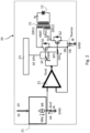
- Figure 2 is a schematic illustration of an ultrasound transmitter device for driving piezoelectric transducers according to the solution described herein, designated as a whole by the reference number 20.
- the central-tap transformer 11 receives a battery voltage VBAT on its own central tap DRVC of the primary winding.
- the transformer 11 is coupled, via its own terminals of the secondary winding, to the piezoelectric transducer 12.
- the terminals DRV1 and DRV2 are coupled, via push-pull MOSFETs Q1 and Q2, to a terminal SN of a sense resistance Rsense, which is in turn coupled, via the other one of its terminals, to a ground terminal GND.
- a digital-to-analog converter 21 receives, from a component represented schematically as a bus 24 operating with a certain number of bits, for example 10 bits, a digital value ID that represents the analog output current of the DAC Idac at the input terminal, represented by a node NR, of an operational amplifier 22, which is also coupled to the ground terminal GND via a reference resistance Rref, the value of which is proportional, by a factor N, preferably an integer, to the value of the sense resistance Rsense.
- the operational amplifier 22 is moreover coupled to the sense terminal SN via the other one of its input terminals.
- the output of the operational amplifier 22 is supplied as driving signal to both of the control electrodes, in particular the gate electrodes, of the pull-push MOSFETs Q1 and Q2.
- Switch SWH and SWL are themselves, for example, obtained using MOSFETs, which are driven into their open and closed states by an overlap-control unit 23, which supplies complementary pulse sequences SP, SPn, i.e., sequences of opening and closing signals; for example, each opening and closing signal is a square-wave signal with variable duty cycle.
- pulse sequence is here meant, for example, a sequence of a PWM (Pulse Width Modulation) type with variable duty cycle, even beyond 50%, as described in what follows.
- the operational amplifier 22 acts as one and the same driving circuit, which drives both of the push-pull MOSFETs Q1 and Q2, and enables an overlap control that maximizes the performance of actuation.
- the operational amplifier 22 is configured for controlling the gate-to-source voltage of the pull-push MOSFETs Q1 and Q2 so as to carry out a pulse modulation of a controlled current Ip that flows in the piezoelectric transducer 12, through the central-tap transformer 11.
- the controlled current Ip has a value that is proportional to the one defined by the DAC 21 and is multiplied by the ratio between the sense resistance Rsense and the reference resistance Rref, hence 1/N.
- the operational amplifier 22 supplies at output a voltage Vout, which, according to which of the switches SWH, SWL on the gates of the two MOSFETs Q1 and Q2 is closed in order to couple the output of the operational amplifier 22 to the respective MOSFET Q1 or Q2, determines an output current Iout, which flows in one of the two branches, DRV1, DRV2 of the primary of the transformer 11.
- the output current Iout is represented as flowing in the branch DRV2 of the MOSFET Q2 in so far as the switch SWL is represented closed, but the switch SWH may conversely be closed, in which case the output current Iout flows in the branch DRV1, or else, as described more fully in what follows, with both switches SWH, SWL on the gates of the two MOSFETs Q1 and Q2 closed, the current Iout flows in a shared way in both of the branches DRV1, DRV2.
- the overlap-control unit 23 carries out overlap control of the output current Iout in the two branches between the output of the operational amplifier 22 and, respectively, the MOSFETs Q1 and Q2, interposed on which are the respective switches SWH and SWL, the aim being to maximize the transmission performance.
- the output current Iout is shared on both of the branches corresponding to the switches SWH and SWL, through both of the MOSFETs Q1 and Q2, for an overlap time imposed by the overlap-control unit 23.
- an operational amplifier 22 is present, through internal compensation in frequency of the aforesaid operational amplifier 22, it is possible to modify the shape of current in the transducer 12, favouring selectively the steady-state accuracy or the speed required to reach an adequate minimum value.
- a value of compensation capacitance may be varied (for example, by adding or removing capacitances in parallel). By reducing the value of compensation capacitance of the amplifier 22, it is possible, for example to render the rising edges of the currents Iout, Ip steeper.
- the use of the operational amplifier 22 enables the current to be shared in the two branches irrespective of any mismatch of threshold voltage Vth1, Vth2 of the two MOSFETs Q1 and Q2, thanks to the virtual ground of the operational amplifier 22.
- a voltage drop VA occurs that is equal to VB, where VB is the voltage drop on the sense resistance Rsense.
- the digital selection of the code corresponding to the digital value Id at input to the DAC 21 determines the output current of the DAC Idac.
- the selection may be made with a coding chosen at will.
- the digital value ID at input to the DAC 21, which determines the analog output current of the DAC Idac, is divided or multiplied to obtain the final current value IA that flows in the reference resistance Rref.
- a constant current value is selected for the time necessary to transmit the desired amplitude.
- the current value is changed also during transmission to increase or reduce the amplitude of the signal transmitted on the transducer 12:
- the DAC 21 must necessarily provide a current output. It is not necessary to limit use to a specific architecture. For instance, for the DAC 21 a configuration may be used with additive and subtractive current mirrors at the output node.
- the DAC 21 is obtained with low-voltage components.
- the transmitted power gradually by increasing the controlled current Ip transmitted until the receiver is able to detect an obstacle.
- the power can subsequently be increased and reduced according to whether the echo is received more or less intensely.
- the circuit described enables this to be obtained via instantaneous modifications of the digital value ID supplied to the DAC 21, for example via a microcontroller.
- a digital combination i.e., a digital value of current ID
- a digital current value ID is sent at input to the DAC 21 with only the LSB (Least Significant Bit) at 1, for a level of current Idac, hence Ip, of minimum value, and with all the bits at 1 for a level of current Idac, hence Ip, of maximum value.
- the current IB in the sense resistance Rsense depends only upon the value of voltage VA present between the reference node NR and ground GND.
- the output current Iout is shared in the two push-pull MOSFETs Q1 and Q2 in a substantially equal amount; that is, for the entire time during which the overlap-control unit 23 keeps the two switches SWH, SWL simultaneously closed, the current in each branch corresponds to IB/2, i.e., half of the sense current IB that flows in the sense resistance Rsense.
- Passage of current from one branch to the other occurs gradually thanks to the regulation of the gate-to-source voltage performed by the amplifier 22, which first regulates the gate-to-source voltage VGS of a single push-pull MOSFET, for example Q1, then regulates both of the gate-to-source voltages, i.e., those corresponding to the MOSFETs Q1 and Q2 closed together, and then once again regulates just one of them, e.g., the gate-to-source voltage VGS of the MOSFET Q2.
- the value of current, equal to the sense current IB, that was present on one branch will be present on the other branch irrespective of the value of threshold voltage Vth of the push-pull MOSFETs Q1 and Q2, since it depends only upon the voltage VA on the regulation node NR.
- the pulse is hence of course symmetrical irrespective of any technological mismatch of the push-pull MOSFETs Q1, Q2.
- an ultrasound transmitter device for driving piezoelectric transducers 20 which comprises a central-tap transformer 11 and a piezoelectric transducer 12 coupled to the terminals of the output secondary winding of the central-tap transformer 11 from which it receives a controlled current Ip to regulate the actuation power thereof.
- the above central-tap transformer 11 comprises a primary winding, which includes terminals DRV1, DRV2 at the ends of said primary winding and a central terminal DRVC that is coupled to a constant d.c. voltage, in particular a battery voltage VBAT of the motor vehicle, the end terminals DRV1, DRV2 being coupled, through respective transistors Q1, Q2, in particular MOSFETs, in particular power MOSFETs, to a ground voltage GND, the transistors Q1, Q2 being driven into their own open and closed states by respective complementary pulse sequences SP, SPn, i.e., sequences of pulses that have prevalently different values, even though it is possible for a non-zero overlap interval to be defined in which they assume the same value.
- the transistors Q1, Q2 operating in push-pull mode are coupled to the ground terminal GND through a sense resistance Rsense.
- a digital-to-analog converter 21 which supplies an analog current Idac to a driving amplifier
- the above circuit arrangement means that it is possible to carry out a current control via a sense resistance of very small dimensions with respect to a power DAC and exploit a resistance N times greater to provide a reference with which to select the power transmitted by the piezoelectric 12.
- the output of the driving amplifier 22 is coupled in parallel, via respective switches SWH, SWL, to respective control electrodes, in particular gate electrodes, of said transistors operating in push-pull mode Q1, Q2, said complementary pulse sequences SP, SPn being supplied as control signals of said respective switches.
- the complementary pulse sequences SP, SPn comprise overlap time intervals in which they have the same logic value, in particular corresponding to a closed state of the respective switches SWH, SWL, and in which complementary pulse sequences SP, SPn are supplied by an overlap-control module 23, configured for controlling said pulse-overlap time at one and the same value in the two sequences.
- the overlap time is in general a time interval during which the complementary pulses SP and SPn have the same value, in particular the same value that drives the switches SWH and SWL into the closed state and the MOSFETs Q1, Q2 into conduction.
- a method for controlling the ultrasound pulse transmitter device 20 may comprise determining a controlled value of current Ip that flows in the piezoelectric transducer 12 in order to regulate the power thereof by setting a digital current value ID at input to the digital-to-analog converter 21.
- a method for controlling the ultrasound pulse transmitter device 20 may comprise, during an operating cycle of the piezoelectric transducer, i.e., for example an obstacle-detection cycle, in which obstacles at different distances are detected in one and the same interval, setting a plurality of different digital values ID in time.
- a method for controlling the ultrasound pulse transmitter device 20 may comprise controlling the overlap time of the complementary pulses via said overlap-control module 23 so as to optimise the operating power.
- the above overlap-control module 23 is configured, for example, for supplying the respective complementary pulse sequences SP, SPn, i.e., sequences of opening and closing signals, to the switch SWH and to the switch SWL, for example each opening and closing signal being a square-wave signal or a PWM signal with variable duty cycle.
- the complementary pulse sequences SP, SPn of the switch SWH and of the switch SWL may in general have a duty cycle of 50% and be complementary to one another; i.e., when the pulses sequence SP of the switch SWH is a closing command, e.g., a high logic level, the complementary pulse sequence SPn of the switch SWL is an opening command, e.g., a low logic level; alternatively, the overlap-control module 23 can determine an overlap time interval, around the instant of switching from closing to opening of one switch and of switching from opening to closing of the other switch, where both the switches SWH, SWL are driven into the closed state; e.g., they both receive a high logic level.
- This overlap interval may, for example, be 10% of the period, and hence, for example, the pulse sequence SP of the switch SWH keeps the latter in the closed state from 0% to 60% of the period of the sequence SP itself, whereas the complementary pulse sequence SPn of the switch SWL keeps the latter in the closed state from 40% to 100% of the period of the complementary sequence SPn of the switch SWL itself.
- the duration of the overlap interval can be controlled by the overlap-control module 23 according to the characteristics of the transducer and to the value of pressure of the piezoelectric that is to be obtained.
- an ultrasonic obstacle detector 50 which comprises a pulse transmitter 20, as described with reference to Figure 2 , that drives the piezoelectric transducer 12, which is an ultrasound transceiver, under the control of the transmission pulse TP sent by the control circuit CM, for emitting ultrasound pulses, i.e., pressure-wave pulses.
- An object 60 located at a distance L reflects the ultrasound waves associated to the ultrasound pulse, which are detected by the piezoelectric transducer 12 itself, the output of which is sent to a receiver circuit 53, which sends a reception control pulse RP to the control circuit CM, which measures the difference in time T between the transmission control pulse TP and the reception control pulse RP.
- the difference in time T is also referred to as "time of flight" and, knowing the speed of propagation of the ultrasound pulse, it is possible to determine the distance L.
- FIG. 3B Illustrated in Figure 3B is a partial block diagram of the ultrasonic obstacle detector 50 comprising the transducer 12, represented schematically as a parallel RC pair, which is driven by the pulse transmitter 20, coupled thereto by a transformer.
- the transducer 12 is moreover coupled for reception to the receiver circuit 53, which in turn comprises an analog-to-digital converter (ADC) 30.
- ADC analog-to-digital converter
- an ultrasound signal RS received which is an analog differential signal, is transmitted by a chain of signals comprising a clamp circuit CP, followed by a low-noise amplifier LNA, in turn followed by a variable-gain amplifier VGA, the gain of which is controlled by the control module CM via a digital-to-analog converter DC1 and which supplies a differential voltage Vdiff to the input of the ADC 30.
Landscapes
- Engineering & Computer Science (AREA)
- Radar, Positioning & Navigation (AREA)
- Remote Sensing (AREA)
- Physics & Mathematics (AREA)
- General Physics & Mathematics (AREA)
- Computer Networks & Wireless Communication (AREA)
- Acoustics & Sound (AREA)
- Mechanical Engineering (AREA)
- Measurement Of Velocity Or Position Using Acoustic Or Ultrasonic Waves (AREA)
Abstract
Description
- The present disclosure relates to an ultrasound transmitter device for driving piezoelectric transducers.
- One or more embodiments may regard ultrasonic obstacle detectors.
- Through stimulation of a piezoelectric transducer it is possible to transmit acoustic waves, in particular ultrasound waves, which can be detected by the transducer itself in order to recognize obstacles.
- The increase in the distance of transmission and the use of specific modulations enable an increase of the performance of ADAS (Advanced Driver Assistance Systems) applications for the automotive market.
- Evolution of basic systems already present on the market makes it possible to pass from diagnostics to assisted/automatic driving.
- Ultrasonic systems must be able to manage problems of environmental interference and interference from systems of adjacent vehicles.
- Wind and rain in fact attenuate and disturb the signal transmitted, whilst pulses coming from adjacent vehicles may give rise to erroneous diagnostics and recognition. Hence, to render the signal more recognizable during reception, it is possible to modulate the transmitted signal (above all, for distances greater than one metre).
- It is, however, difficult to provide a system capable of recognizing simultaneously objects that are far away and objects that are near.
- Reaching great distances of detection implies having to use high current levels in the stimulation of the piezoelectric transducer. It is useful to have a good efficiency of transmission to facilitate operation of the reception stage. Detecting obstacles that are very close means reducing to a minimum the current with which the transducer is stimulated to prevent saturation of the reception stage.
- Present on the market are various ultrasonic systems for obstacle recognition that implement known solutions to achieve the current levels of performance.
- Such systems are costly and present limitations in their performance.
- In general, the application envisages exploitation of a central-tap transformer for driving a piezoelectric transducer at high voltages.
- Illustrated schematically in
Figure 1 is a circuit exemplifying the above known solution, designated as a whole by 10, in which a central-tap transformer 11 has apiezoelectric transducer 12 coupled to the terminals of the secondary winding. Also represented in the figure is coupling of thepiezoelectric transducer 12 to areceiver 53, described more fully with reference toFigure 3B in what follows. The essential components ofFigure 1 are here described briefly to enable understanding of operation of the solution according to the prior art. - Through a
battery 13 that supplies a constant d.c. voltage VBAT, which corresponds to a power supply voltage of 12 V, a central tap DRVC of atransformer 11 is, for example, supplied, while the other two ends DRV1 and DRV2 are alternatively shorted to ground GND by respective transistors Q1 and Q2 coupled thereto operating in push-pull mode, which are power MOSFETs. Complementary pulse sequences SP and SPn, i.e., of pulses having opposite logic levels at the same instant, are supplied by a pulse generator (not illustrated) to the control electrodes of the push-pull transistors Q1 and Q2 so as to bring about opposite open and closed states, i.e., so as to get them to operate in push-pull mode. In this way, the current flows alternatively in the two branches associated to the terminals DRV1, DRVC and DRV2, DRVC, coupling, in two opposite directions, to the secondary winding of thetransformer 11, where also shown is an RC filter formed by a filter resistance Rf and a filter capacitor Cf. Hence, a sinusoidal waveform (given that the filter is an intrinsic filter with a high resonance coefficient Q) is generated on the load, i.e., thepiezoelectric transducer 12. - The amplitude of the voltage on the piezoelectric 12 depends upon the level of current that flows in the branches of the primary of the
transformer 11. - The simplest implementation envisages limitation of the current value through a series resistance, such as the resistance R2 in
Figure 1 , between the battery voltage VBAT and the central tap DRVC of thetransformer 11. - Alternatively, a series of pulses may be generated with the possibility of controlling the power transmitted through the duty cycle.
- This solution is easy to implement, but does not enable precise regulation of the transmitted power, which to a first approximation depends upon the current that passes in the transducer.
- According to the piezoelectric crystal being used, it is possible to maximize the current/pressure efficiency through an overlap control, i.e., a control of overlapping of the pulsed currents transmitted by the two MOSFETs. For instance, if the currents that flow in the two branches overlap for an overlap time interval that forms a part of the respective duty cycle, the current/pressure efficiency of the piezoelectric, in types of piezoelectric crystal or PMUT (Piezoelectric Micromachined Ultrasound Transducer), remains constant up to given values of overlap time interval, and then drops sharply when the time overlap interval exceeds said given values.
- Also to be avoided is the lack of overlap of the currents in the two branches, which may lead to a loss of efficiency and, given the inductances involved, may trigger phenomena of voltage spikes.
- It is, however, difficult to control overlap of the two MOSFETs operating in push-pull mode, i.e., the period during which they remain simultaneously on, since the current value is not known beforehand given that it is dependent upon the process (it does not maximize efficiency in transmission).
- The solution renders transmission asymmetrical since it is unable to control beforehand the level of current in the two branches, which depends upon the MOSFETs used and upon the external componentry.
- An evolution of the system envisages regulation of the current through a generator set in series to the two MOSFETs.
- Standard solutions may be represented by a series of current branches to be selected to obtain the desired level or else a DAC with a power output.
- In the latter case, the drain-to-source on resistance, RDSon, of the pulser is markedly dependent upon the current generator (DAC), and the solution involves a higher occupation of area.
- Providing a power DAC that is effective both at high currents and at low currents is also very complex in terms of linearity.
- Given the aforesaid extensive developments in the field, there is still felt the need for improved solutions, for example to render the circuit flexible and increase its performance both for high currents and for low currents using the same circuitry.
- The object of one or more embodiments is to contribute to meeting the above need.
- According to one or more embodiments, the above object can be achieved thanks to a transmitter device having the characteristics recalled in the ensuing claims.
- One or more embodiments may regard a corresponding ultrasonic detector, as well as a corresponding method.
- The claims form an integral part of the technical teachings provided herein in relation to one or more embodiments.
- As mentioned previously, the present disclosure describes solutions regarding an ultrasound transmitter device for driving piezoelectric transducers,
- comprising a central-tap transformer and a piezoelectric transducer coupled to the terminals of the secondary output winding of said central-tap transformer from which it receives a controlled current,
- said central-tap transformer including a primary winding comprising terminals at the ends said primary winding and a central terminal, said central terminal being coupled to a constant d.c. voltage, in particular a battery voltage, said end terminals being coupled, via respective transistors, in particular MOSFETs, to a ground voltage, said transistors being driven into their own states of conduction and inhibition by respective complementary pulse sequences, wherein:
- said transistors are coupled to said ground terminal through a sense resistance,
- said transmitter device comprising a digital-to-analog converter, which supplies an analog current to a driving amplifier, which in turn supplies a driving current to said transistors,
- the output of said digital-to-analog converter being coupled to an input terminal of the driving amplifier, which is also coupled to the ground terminal through a reference resistance that has a value proportional to, in particular a multiple or a divisor of, the value of the sense resistance,
- said sense resistance being coupled to the other input terminal of the driving amplifier.
- In variant embodiments, said output of said driving amplifier is coupled in parallel, through respective switches, to respective control electrodes, in particular gate electrodes, of said transistors, said complementary pulse sequences being supplied as control signals of said respective switches.
- In variant embodiments, said complementary pulse sequences comprise overlap time intervals during which said complementary pulse sequences have the same logic value, in particular corresponding to a closed state of the respective switches, and during which said complementary pulse sequences are supplied by an overlap-control module, configured for controlling said pulse-overlap time at one and the same value in the two sequences.
- The present disclosure also regards an ultrasonic obstacle detector comprising an ultrasound pulse transmitter device according to various embodiments.
- The present disclosure also regards a method for controlling an ultrasound transmitter device according to various embodiments that envisages determining the flowing flow of a current with controlled value in the piezoelectric transducer by setting a digital value of current at input to the digital-to-analog converter.
- In variant embodiments, during an operating cycle of the piezoelectric transducer a plurality of different digital current values is set in time.
- In variant embodiments, the overlap time of the complementary pulses is controlled via said overlap-control module.
- One or more embodiments are able to afford one or more of the following advantages:
- symmetry independent of the external components;
- good accuracy;
- compact solution; and
- additional functions for controlling the overlap and shape of the current.
- One or more embodiments will now be described, purely by way of non-limiting example, with reference to the annexed drawings, wherein:
-
Figure 1 has already been described previously; -
Figure 2 is a schematic representation of a device according to the solution described herein; and -
Figures 3A and 3B are schematic representations of an ultrasonic obstacle detector that uses the device according to the solution described herein. - In the ensuing description various specific details are illustrated in order to enable an in-depth understanding of various examples of embodiments according to the description. The embodiments may be obtained without one or more of the specific details, or with other methods, components, materials, etc. In other cases, known structures, materials, or operations are not illustrated or described in detail so that the various aspects of the embodiments will not be obscured. Reference to "an embodiment" or "one embodiment" in the framework of the present description is intended to indicate that a particular configuration, structure, or characteristic described in relation to the embodiment is comprised in at least one embodiment. Hence, phrases such as "in an embodiment" or "in one embodiment" that may be present in various points of the present description do not necessarily refer exactly to one and the same embodiment. Moreover, particular conformations, structures, or characteristics may be combined in any adequate way in one or more embodiments.
- The references used herein are provided merely for convenience and hence do not define the sphere of protection or the scope of the embodiments.
- From what has been described above as regards the prior art, it may be noted how it is important to obtain two drivers capable of switching on and switching off rapidly the two transmission power transistors, in particular power MOSFETs.
- The solution described herein hence comprises a control of the level of current supplied to the central tap of the
transformer 11 via a sense resistance of very small dimensions, in particular small as compared to a power DAC, and further comprises exploitation of a resistance that is a multiple of the sense resistance by a given number N of times in order to provide a resistance reference with which to select the transmitted power. - In this regard,
Figure 2 is a schematic illustration of an ultrasound transmitter device for driving piezoelectric transducers according to the solution described herein, designated as a whole by thereference number 20. - The central-
tap transformer 11 receives a battery voltage VBAT on its own central tap DRVC of the primary winding. Thetransformer 11 is coupled, via its own terminals of the secondary winding, to thepiezoelectric transducer 12. The terminals DRV1 and DRV2 are coupled, via push-pull MOSFETs Q1 and Q2, to a terminal SN of a sense resistance Rsense, which is in turn coupled, via the other one of its terminals, to a ground terminal GND. - A digital-to-
analog converter 21 receives, from a component represented schematically as abus 24 operating with a certain number of bits, for example 10 bits, a digital value ID that represents the analog output current of the DAC Idac at the input terminal, represented by a node NR, of anoperational amplifier 22, which is also coupled to the ground terminal GND via a reference resistance Rref, the value of which is proportional, by a factor N, preferably an integer, to the value of the sense resistance Rsense. Theoperational amplifier 22 is moreover coupled to the sense terminal SN via the other one of its input terminals. The output of theoperational amplifier 22 is supplied as driving signal to both of the control electrodes, in particular the gate electrodes, of the pull-push MOSFETs Q1 and Q2. Set between the output of theoperational amplifier 22 and the control electrodes, in particular the gate electrodes, of the pull-push MOSFETs Q1 and Q2 are respective switches SWH and SWL, which are themselves, for example, obtained using MOSFETs, which are driven into their open and closed states by an overlap-control unit 23, which supplies complementary pulse sequences SP, SPn, i.e., sequences of opening and closing signals; for example, each opening and closing signal is a square-wave signal with variable duty cycle. It should be noted that by "pulse sequence" is here meant, for example, a sequence of a PWM (Pulse Width Modulation) type with variable duty cycle, even beyond 50%, as described in what follows. - Hence, the
operational amplifier 22 acts as one and the same driving circuit, which drives both of the push-pull MOSFETs Q1 and Q2, and enables an overlap control that maximizes the performance of actuation. - The
operational amplifier 22 is configured for controlling the gate-to-source voltage of the pull-push MOSFETs Q1 and Q2 so as to carry out a pulse modulation of a controlled current Ip that flows in thepiezoelectric transducer 12, through the central-tap transformer 11. The controlled current Ip has a value that is proportional to the one defined by theDAC 21 and is multiplied by the ratio between the sense resistance Rsense and the reference resistance Rref, hence 1/N. - The
operational amplifier 22 supplies at output a voltage Vout, which, according to which of the switches SWH, SWL on the gates of the two MOSFETs Q1 and Q2 is closed in order to couple the output of theoperational amplifier 22 to the respective MOSFET Q1 or Q2, determines an output current Iout, which flows in one of the two branches, DRV1, DRV2 of the primary of thetransformer 11. InFigure 2 , the output current Iout is represented as flowing in the branch DRV2 of the MOSFET Q2 in so far as the switch SWL is represented closed, but the switch SWH may conversely be closed, in which case the output current Iout flows in the branch DRV1, or else, as described more fully in what follows, with both switches SWH, SWL on the gates of the two MOSFETs Q1 and Q2 closed, the current Iout flows in a shared way in both of the branches DRV1, DRV2. - The overlap-
control unit 23 carries out overlap control of the output current Iout in the two branches between the output of theoperational amplifier 22 and, respectively, the MOSFETs Q1 and Q2, interposed on which are the respective switches SWH and SWL, the aim being to maximize the transmission performance. By keeping simultaneously on the two switches SWH and SWL coupled to the gates of the MOSFETs Q1 and Q2 that regulate the controlled current Ip, the output current Iout is shared on both of the branches corresponding to the switches SWH and SWL, through both of the MOSFETs Q1 and Q2, for an overlap time imposed by the overlap-control unit 23. - Since an
operational amplifier 22 is present, through internal compensation in frequency of the aforesaidoperational amplifier 22, it is possible to modify the shape of current in thetransducer 12, favouring selectively the steady-state accuracy or the speed required to reach an adequate minimum value. In particular, to vary the internal frequency compensation, as is known, a value of compensation capacitance may be varied (for example, by adding or removing capacitances in parallel). By reducing the value of compensation capacitance of theamplifier 22, it is possible, for example to render the rising edges of the currents Iout, Ip steeper. - Furthermore, the use of the
operational amplifier 22 enables the current to be shared in the two branches irrespective of any mismatch of threshold voltage Vth1, Vth2 of the two MOSFETs Q1 and Q2, thanks to the virtual ground of theoperational amplifier 22. - On the reference resistance Rref a voltage drop VA occurs that is equal to VB, where VB is the voltage drop on the sense resistance Rsense.
- As regards the current, the digital selection of the code corresponding to the digital value Id at input to the
DAC 21 determines the output current of the DAC Idac. The selection may be made with a coding chosen at will. - A current IA that flows in the reference resistance Rref and a current IB that flows in the sense resistance are proportional through the multiplying number N, i.e., IB = N·IA. Hence, the digital value ID at input to the
DAC 21, which determines the analog output current of the DAC Idac, is divided or multiplied to obtain the final current value IA that flows in the reference resistance Rref. - A constant current value is selected for the time necessary to transmit the desired amplitude.
- The current value is changed also during transmission to increase or reduce the amplitude of the signal transmitted on the transducer 12:
-

-

- The
DAC 21 must necessarily provide a current output. It is not necessary to limit use to a specific architecture. For instance, for the DAC 21 a configuration may be used with additive and subtractive current mirrors at the output node. - The
DAC 21 is obtained with low-voltage components. - Corresponding to each current level is a different voltage value that develops on the regulation node SN:
- a low current value implies a lower power of actuation of the piezoelectric 12;
- a high current value implies a high power of actuation of the piezoelectric 12.
- It is possible to create different driving profiles as a function of the distance at which the
transducer 12 is to operate and to regulate via the digital value ID supplied to theDAC 21 the controlled current Ip on a number of levels over a given time period, corresponding to an operating cycle, to be able to cover different distances. - For instance, in the case of a distant obstacle, it is possible to increase the transmitted power gradually by increasing the controlled current Ip transmitted until the receiver is able to detect an obstacle. The power can subsequently be increased and reduced according to whether the echo is received more or less intensely. The circuit described enables this to be obtained via instantaneous modifications of the digital value ID supplied to the
DAC 21, for example via a microcontroller. - Hence, a digital combination, i.e., a digital value of current ID, at input to the
DAC 21 is used to reduce or increase the controlled current Ip. Purely by way of non-limiting example, a digital current value ID is sent at input to theDAC 21 with only the LSB (Least Significant Bit) at 1, for a level of current Idac, hence Ip, of minimum value, and with all the bits at 1 for a level of current Idac, hence Ip, of maximum value. - The current IB in the sense resistance Rsense depends only upon the value of voltage VA present between the reference node NR and ground GND.
- At the instant when both of the switches SWH, SWL are simultaneously closed, the output current Iout is shared in the two push-pull MOSFETs Q1 and Q2 in a substantially equal amount; that is, for the entire time during which the overlap-
control unit 23 keeps the two switches SWH, SWL simultaneously closed, the current in each branch corresponds to IB/2, i.e., half of the sense current IB that flows in the sense resistance Rsense. - When the switches SWH, SWL change state, so that one remains in the closed state while the other goes into the open state, the current IB/2 in the branch corresponding to the latter switch vanishes, whereas all the sense current IB flows in the other branch, where the switch is closed.
- Passage of current from one branch to the other occurs gradually thanks to the regulation of the gate-to-source voltage performed by the
amplifier 22, which first regulates the gate-to-source voltage VGS of a single push-pull MOSFET, for example Q1, then regulates both of the gate-to-source voltages, i.e., those corresponding to the MOSFETs Q1 and Q2 closed together, and then once again regulates just one of them, e.g., the gate-to-source voltage VGS of the MOSFET Q2. - At the end of the transition, the value of current, equal to the sense current IB, that was present on one branch will be present on the other branch irrespective of the value of threshold voltage Vth of the push-pull MOSFETs Q1 and Q2, since it depends only upon the voltage VA on the regulation node NR. The pulse is hence of course symmetrical irrespective of any technological mismatch of the push-pull MOSFETs Q1, Q2.
- Hence, basically represented in
Figure 2 is an ultrasound transmitter device for drivingpiezoelectric transducers 20, which comprises a central-tap transformer 11 and apiezoelectric transducer 12 coupled to the terminals of the output secondary winding of the central-tap transformer 11 from which it receives a controlled current Ip to regulate the actuation power thereof. - The above central-
tap transformer 11 comprises a primary winding, which includes terminals DRV1, DRV2 at the ends of said primary winding and a central terminal DRVC that is coupled to a constant d.c. voltage, in particular a battery voltage VBAT of the motor vehicle, the end terminals DRV1, DRV2 being coupled, through respective transistors Q1, Q2, in particular MOSFETs, in particular power MOSFETs, to a ground voltage GND, the transistors Q1, Q2 being driven into their own open and closed states by respective complementary pulse sequences SP, SPn, i.e., sequences of pulses that have prevalently different values, even though it is possible for a non-zero overlap interval to be defined in which they assume the same value. - The transistors Q1, Q2 operating in push-pull mode are coupled to the ground terminal GND through a sense resistance Rsense.
- The
transmitter device 20 then comprises a digital-to-analog converter 21, which supplies an analog current Idac to a drivingamplifier 22, for example obtained via an operational amplifier, which drives the flow of a driving current Iout - in particular by imposing on the sense resistance Rsense a voltage drop VB equal to the voltage drop VA on the reference resistance Rref, VA = VB, where VB is the voltage drop on the sense resistance Rsense - in the above transistors Q1, Q2 operating in push-pull mode, in particular by controlling their gate-to-source voltage, the output of the digital-to-analog converter being coupled to an input terminal NR of the drivingamplifier 22, which is also coupled to the ground terminal GND through a reference resistance Rref, which has a value, N, that is proportional to, in particular a multiple or a divisor of, the value of the sense resistance Rsense, which is finally coupled to the other input terminal of the drivingamplifier 22. - The above circuit arrangement means that it is possible to carry out a current control via a sense resistance of very small dimensions with respect to a power DAC and exploit a resistance N times greater to provide a reference with which to select the power transmitted by the piezoelectric 12.
- Moreover, the output of the driving
amplifier 22 is coupled in parallel, via respective switches SWH, SWL, to respective control electrodes, in particular gate electrodes, of said transistors operating in push-pull mode Q1, Q2, said complementary pulse sequences SP, SPn being supplied as control signals of said respective switches. - This means using the same driver for driving both of the power transmission MOSFETs, where the virtual ground of the operational amplifier renders operation independent of the threshold voltages of the push-pull transistors Q1, Q2.
- Furthermore, the complementary pulse sequences SP, SPn comprise overlap time intervals in which they have the same logic value, in particular corresponding to a closed state of the respective switches SWH, SWL, and in which complementary pulse sequences SP, SPn are supplied by an overlap-
control module 23, configured for controlling said pulse-overlap time at one and the same value in the two sequences. Hence, the overlap time is in general a time interval during which the complementary pulses SP and SPn have the same value, in particular the same value that drives the switches SWH and SWL into the closed state and the MOSFETs Q1, Q2 into conduction. - This means using the same driver for driving both of the power transmission MOSFETs, it then being possible to provide an overlap control that can maximize the performance of actuation of the piezoelectric 12.
- Hence, a method for controlling the ultrasound
pulse transmitter device 20 may comprise determining a controlled value of current Ip that flows in thepiezoelectric transducer 12 in order to regulate the power thereof by setting a digital current value ID at input to the digital-to-analog converter 21. - Furthermore, a method for controlling the ultrasound
pulse transmitter device 20 may comprise, during an operating cycle of the piezoelectric transducer, i.e., for example an obstacle-detection cycle, in which obstacles at different distances are detected in one and the same interval, setting a plurality of different digital values ID in time. - Moreover, a method for controlling the ultrasound
pulse transmitter device 20 may comprise controlling the overlap time of the complementary pulses via said overlap-control module 23 so as to optimise the operating power. The above overlap-control module 23 is configured, for example, for supplying the respective complementary pulse sequences SP, SPn, i.e., sequences of opening and closing signals, to the switch SWH and to the switch SWL, for example each opening and closing signal being a square-wave signal or a PWM signal with variable duty cycle. The complementary pulse sequences SP, SPn of the switch SWH and of the switch SWL may in general have a duty cycle of 50% and be complementary to one another; i.e., when the pulses sequence SP of the switch SWH is a closing command, e.g., a high logic level, the complementary pulse sequence SPn of the switch SWL is an opening command, e.g., a low logic level; alternatively, the overlap-control module 23 can determine an overlap time interval, around the instant of switching from closing to opening of one switch and of switching from opening to closing of the other switch, where both the switches SWH, SWL are driven into the closed state; e.g., they both receive a high logic level. This overlap interval may, for example, be 10% of the period, and hence, for example, the pulse sequence SP of the switch SWH keeps the latter in the closed state from 0% to 60% of the period of the sequence SP itself, whereas the complementary pulse sequence SPn of the switch SWL keeps the latter in the closed state from 40% to 100% of the period of the complementary sequence SPn of the switch SWL itself. The duration of the overlap interval can be controlled by the overlap-control module 23 according to the characteristics of the transducer and to the value of pressure of the piezoelectric that is to be obtained. - Illustrated in
Figure 3A is anultrasonic obstacle detector 50, which comprises apulse transmitter 20, as described with reference toFigure 2 , that drives thepiezoelectric transducer 12, which is an ultrasound transceiver, under the control of the transmission pulse TP sent by the control circuit CM, for emitting ultrasound pulses, i.e., pressure-wave pulses. - An
object 60 located at a distance L reflects the ultrasound waves associated to the ultrasound pulse, which are detected by thepiezoelectric transducer 12 itself, the output of which is sent to areceiver circuit 53, which sends a reception control pulse RP to the control circuit CM, which measures the difference in time T between the transmission control pulse TP and the reception control pulse RP. The difference in time T is also referred to as "time of flight" and, knowing the speed of propagation of the ultrasound pulse, it is possible to determine the distance L. - Illustrated in
Figure 3B is a partial block diagram of theultrasonic obstacle detector 50 comprising thetransducer 12, represented schematically as a parallel RC pair, which is driven by thepulse transmitter 20, coupled thereto by a transformer. Thetransducer 12 is moreover coupled for reception to thereceiver circuit 53, which in turn comprises an analog-to-digital converter (ADC) 30. Consequently, as illustrated inFigure 3B , an ultrasound signal RS received, which is an analog differential signal, is transmitted by a chain of signals comprising a clamp circuit CP, followed by a low-noise amplifier LNA, in turn followed by a variable-gain amplifier VGA, the gain of which is controlled by the control module CM via a digital-to-analog converter DC1 and which supplies a differential voltage Vdiff to the input of theADC 30. The digital output DO or the filtered digital output DF of theADC 30, which in general may comprise the reception control pulse RP, is supplied to a control module CM, which, as has been said, is configured for computing the distance L from the object on the basis of the time of flight of the ultrasound pulse between thetransmitter 20 and thereceiver 53. - Consequently, the advantages of the solution described emerge clearly.
- The solution described makes it possible to render the circuit flexible and efficient in its performance both for high currents and for low currents using one and the same circuitry.
- The solution moreover affords the following advantages:
- symmetry independent of the external components, in particular on account of the independence from the threshold voltages of the transistors;
- good accuracy;
- compact solution; and
- additional functions for control of overlap and shape of the current.
- Without prejudice to the underlying principles, the details of construction and the embodiments may vary, even significantly, with respect to what has been illustrated herein purely by way of non-limiting example, without thereby departing from the sphere of protection, as this is defined by the annexed claims.
Claims (7)
- Ultrasound transmitter device for driving piezoelectric transducers,comprising a central tap transformed (11) and a piezoelectric transducer (12) coupled to the terminals of the secondary output winding of said central tap transformer (11) from which receives a controlled current (Ip),said central tap transformer (11) comprising a primary winding comprising terminals (DRV1, DRV2) at the ends of said primary windings and a central terminal (DRVC), said central terminal (DRVC) being coupled to a constant direct voltage, in particular a battery voltage (VBAT), said terminals at the ends (DRV1, DRV2) being coupled through respective transistors (Q1, Q2), in particular MOSFET, operating as push pull at a ground voltage (GND), said transistor (Q1, Q2) operating as push pull being commanded in their opening and closure states by respective complementary pulses sequences (SP, SPn), whereinsaid transmitter device (20) comprises a digital to analog converter (21) supplying an analog current (Idac) to a driver amplifier (22) configured to determine the flowing of a driving current (Iout) in said transistors (Q1, Q2) operating as push pull,said transistors (Q1, Q2) operating as push pull being coupled to said ground terminal (GND) through a sense resistance (Rsense),the output of said digital to analog converter (21) being coupled to an input terminal (NR) of the driver amplifier (22) which is also coupled to the ground terminal (GND) through a reference resistance (Rref) which has a proportional value, in particular a multiple or a divider, with respect to the value of the sense resistance (Rsense),said sense resistance (Rsense) being coupled to the other input terminal of the driver amplifier (22).
- Device according to claim 1, wherein said output of said driver amplifier (22) is coupled through respective switches (SWH, SWL) to respective control electrodes, in particular gate electrodes, of said transistors (Q1, Q2), said complementary pulse sequences (SP, SPn) being supplied as control signals of said respective switches.
- Device according to claim 1 or 2, wherein said complementary pulse sequences (SP, SPn) comprise overlapping time intervals in which said complementary pulse sequences (SP, SPn) have the same logic value, in particular corresponding to a closed state of the respective switches (SWH, SWL), and in which said complementary pulse sequences (SP, SPn) are provided by an overlap control module (23), configured to control said pulse overlap time to have the same value in the two sequences.
- Ultrasonic obstacle detector comprising an ultrasound transmitter device according to any of claims 1 to 3.
- Method for controlling an ultrasound transmitter device according to any of claims 1 to 3, characterized by
determining a controlled current value (Ip) flowing in the piezoelectric transducer (12) by setting a digital signal value (ID) at the input of the digital to analog converter (21). - Method according to claim 5, wherein during an operating cycle of the piezoelectric transducer (12) a plurality of different digital signal values (ID) are set over time.
- Method according to claim 5 or 6, wherein it is controlled an overlap time of the complementary pulses (SP, SPn) by said overlap control module (23).
Applications Claiming Priority (1)
| Application Number | Priority Date | Filing Date | Title |
|---|---|---|---|
| IT102022000005384A IT202200005384A1 (en) | 2022-03-18 | 2022-03-18 | ULTRASONIC TRANSMITTER DEVICE FOR DRIVING PIEZOELECTRIC TRANSDUCERS |
Publications (1)
| Publication Number | Publication Date |
|---|---|
| EP4246179A1 true EP4246179A1 (en) | 2023-09-20 |
Family
ID=81851283
Family Applications (1)
| Application Number | Title | Priority Date | Filing Date |
|---|---|---|---|
| EP23158628.0A Withdrawn EP4246179A1 (en) | 2022-03-18 | 2023-02-24 | Ultrasound transmitter device for driving piezoelectric transducers |
Country Status (3)
| Country | Link |
|---|---|
| US (1) | US12130360B2 (en) |
| EP (1) | EP4246179A1 (en) |
| IT (1) | IT202200005384A1 (en) |
Citations (4)
| Publication number | Priority date | Publication date | Assignee | Title |
|---|---|---|---|---|
| US3919655A (en) * | 1973-12-26 | 1975-11-11 | Electronics Research Group Inc | High power operational amplifier |
| US20030164658A1 (en) * | 2002-03-04 | 2003-09-04 | Cepheid | Method and apparatus for controlling ultrasonic transducer |
| US20040158147A1 (en) * | 2003-02-10 | 2004-08-12 | Siemens Medical Solutions Usa, Inc. | Transmit circuit for imaging with ultrasound |
| JP2008237280A (en) * | 2007-03-26 | 2008-10-09 | Hitachi Medical Corp | Ultrasonic diagnostic apparatus |
-
2022
- 2022-03-18 IT IT102022000005384A patent/IT202200005384A1/en unknown
-
2023
- 2023-02-24 EP EP23158628.0A patent/EP4246179A1/en not_active Withdrawn
- 2023-03-03 US US18/178,110 patent/US12130360B2/en active Active
Patent Citations (4)
| Publication number | Priority date | Publication date | Assignee | Title |
|---|---|---|---|---|
| US3919655A (en) * | 1973-12-26 | 1975-11-11 | Electronics Research Group Inc | High power operational amplifier |
| US20030164658A1 (en) * | 2002-03-04 | 2003-09-04 | Cepheid | Method and apparatus for controlling ultrasonic transducer |
| US20040158147A1 (en) * | 2003-02-10 | 2004-08-12 | Siemens Medical Solutions Usa, Inc. | Transmit circuit for imaging with ultrasound |
| JP2008237280A (en) * | 2007-03-26 | 2008-10-09 | Hitachi Medical Corp | Ultrasonic diagnostic apparatus |
Also Published As
| Publication number | Publication date |
|---|---|
| IT202200005384A1 (en) | 2023-09-18 |
| US20230296769A1 (en) | 2023-09-21 |
| US12130360B2 (en) | 2024-10-29 |
Similar Documents
| Publication | Publication Date | Title |
|---|---|---|
| EP0314386B1 (en) | A power supply | |
| EP1421830B1 (en) | Led-driver apparatus | |
| EP0967722B1 (en) | Switching arrangement | |
| US10250145B2 (en) | Device for avoiding hard switching in resonant converter and related method | |
| US8232789B2 (en) | System and method for providing linear buck boost transitions within a buck boost converter | |
| US8593123B2 (en) | Switching voltage regulators with hysteretic control for enhanced mode-transition speed and stability | |
| US7372240B2 (en) | Output load adaptable MOSFET gate drive voltage level in a DC-DC controller | |
| US7729140B2 (en) | Sampling method with adjusting duty ratios | |
| US20210218223A1 (en) | Pulse generator circuit, related laser system and method | |
| GB2372329A (en) | Ground mineralisation rejecting metal detector | |
| CN221148931U (en) | Ultrasonic emitter device, ultrasonic obstacle detector and circuit | |
| US8159792B2 (en) | Motor control device | |
| US12130360B2 (en) | Ultrasound transmitter device for driving piezoelectric transducers | |
| CN111224551A (en) | power converter | |
| US10587192B2 (en) | DC-DC voltage reducing converter with a test mode operation | |
| KR20220161025A (en) | Apparatus for operation of buck-boost converter | |
| US20040100750A1 (en) | Interface circuit with power converter with interface circuit and electric vehicle with power converter | |
| US7973588B2 (en) | Analog insulation/multiplexer | |
| US20100085027A1 (en) | System and method for providing linear buck boost transitions within a buck boost converter | |
| US8487482B2 (en) | Circuit for controlling power supply to a consumer and method for operating a circuit | |
| RU2003100736A (en) | METHOD FOR CONTROL PULSE VOLTAGE STABILIZER | |
| WO1997044884A1 (en) | Switching power source circuit | |
| US20060152270A1 (en) | Circuit arrangement for electrically isolated signal transmission | |
| WO2020243891A1 (en) | Apparatus and method for power conversion | |
| US12407345B2 (en) | Switched inductive storage element to enhance gate drive at turn-off |
Legal Events
| Date | Code | Title | Description |
|---|---|---|---|
| PUAI | Public reference made under article 153(3) epc to a published international application that has entered the european phase |
Free format text: ORIGINAL CODE: 0009012 |
|
| STAA | Information on the status of an ep patent application or granted ep patent |
Free format text: STATUS: THE APPLICATION HAS BEEN PUBLISHED |
|
| AK | Designated contracting states |
Kind code of ref document: A1 Designated state(s): AL AT BE BG CH CY CZ DE DK EE ES FI FR GB GR HR HU IE IS IT LI LT LU LV MC ME MK MT NL NO PL PT RO RS SE SI SK SM TR |
|
| STAA | Information on the status of an ep patent application or granted ep patent |
Free format text: STATUS: REQUEST FOR EXAMINATION WAS MADE |
|
| 17P | Request for examination filed |
Effective date: 20240318 |
|
| RBV | Designated contracting states (corrected) |
Designated state(s): AL AT BE BG CH CY CZ DE DK EE ES FI FR GB GR HR HU IE IS IT LI LT LU LV MC ME MK MT NL NO PL PT RO RS SE SI SK SM TR |
|
| STAA | Information on the status of an ep patent application or granted ep patent |
Free format text: STATUS: THE APPLICATION HAS BEEN WITHDRAWN |
|
| 18W | Application withdrawn |
Effective date: 20251201 |