EP4246155A1 - Semiconductor devices comprising failure detectors for detecting failures of bipolar junction transistors - Google Patents
Semiconductor devices comprising failure detectors for detecting failures of bipolar junction transistors Download PDFInfo
- Publication number
- EP4246155A1 EP4246155A1 EP23159073.8A EP23159073A EP4246155A1 EP 4246155 A1 EP4246155 A1 EP 4246155A1 EP 23159073 A EP23159073 A EP 23159073A EP 4246155 A1 EP4246155 A1 EP 4246155A1
- Authority
- EP
- European Patent Office
- Prior art keywords
- vbe
- voltage
- base
- bipolar junction
- junction transistor
- Prior art date
- Legal status (The legal status is an assumption and is not a legal conclusion. Google has not performed a legal analysis and makes no representation as to the accuracy of the status listed.)
- Granted
Links
Images








Classifications
-
- G—PHYSICS
- G01—MEASURING; TESTING
- G01R—MEASURING ELECTRIC VARIABLES; MEASURING MAGNETIC VARIABLES
- G01R31/00—Arrangements for testing electric properties; Arrangements for locating electric faults; Arrangements for electrical testing characterised by what is being tested not provided for elsewhere
- G01R31/26—Testing of individual semiconductor devices
- G01R31/2607—Circuits therefor
- G01R31/2608—Circuits therefor for testing bipolar transistors
- G01R31/2619—Circuits therefor for testing bipolar transistors for measuring thermal properties thereof
-
- G—PHYSICS
- G01—MEASURING; TESTING
- G01K—MEASURING TEMPERATURE; MEASURING QUANTITY OF HEAT; THERMALLY-SENSITIVE ELEMENTS NOT OTHERWISE PROVIDED FOR
- G01K15/00—Testing or calibrating of thermometers
- G01K15/007—Testing
-
- G—PHYSICS
- G01—MEASURING; TESTING
- G01K—MEASURING TEMPERATURE; MEASURING QUANTITY OF HEAT; THERMALLY-SENSITIVE ELEMENTS NOT OTHERWISE PROVIDED FOR
- G01K7/00—Measuring temperature based on the use of electric or magnetic elements directly sensitive to heat ; Power supply therefor, e.g. using thermoelectric elements
- G01K7/01—Measuring temperature based on the use of electric or magnetic elements directly sensitive to heat ; Power supply therefor, e.g. using thermoelectric elements using semiconducting elements having PN junctions
-
- G—PHYSICS
- G01—MEASURING; TESTING
- G01R—MEASURING ELECTRIC VARIABLES; MEASURING MAGNETIC VARIABLES
- G01R19/00—Arrangements for measuring currents or voltages or for indicating presence or sign thereof
- G01R19/10—Measuring sum, difference or ratio
-
- G—PHYSICS
- G01—MEASURING; TESTING
- G01R—MEASURING ELECTRIC VARIABLES; MEASURING MAGNETIC VARIABLES
- G01R31/00—Arrangements for testing electric properties; Arrangements for locating electric faults; Arrangements for electrical testing characterised by what is being tested not provided for elsewhere
- G01R31/26—Testing of individual semiconductor devices
- G01R31/2607—Circuits therefor
- G01R31/2608—Circuits therefor for testing bipolar transistors
-
- H—ELECTRICITY
- H10—SEMICONDUCTOR DEVICES; ELECTRIC SOLID-STATE DEVICES NOT OTHERWISE PROVIDED FOR
- H10D—INORGANIC ELECTRIC SEMICONDUCTOR DEVICES
- H10D84/00—Integrated devices formed in or on semiconductor substrates that comprise only semiconducting layers, e.g. on Si wafers or on GaAs-on-Si wafers
- H10D84/60—Integrated devices formed in or on semiconductor substrates that comprise only semiconducting layers, e.g. on Si wafers or on GaAs-on-Si wafers characterised by the integration of at least one component covered by groups H10D10/00 or H10D18/00, e.g. integration of BJTs
- H10D84/611—Combinations of BJTs and one or more of diodes, resistors or capacitors
Definitions
- aspects of the inventive concepts relate to semiconductor devices, and more particularly, to semiconductor devices that include a detector for detecting an error or a failure of a bipolar junction transistor, and to methods for detecting a failure of a bipolar junction transistor.
- a temperature sensor which is a core component of a temperature management system, is generally implemented using a bipolar junction transistor BJT. More specifically, conventional bipolar junction transistor BJT based temperature sensors may sense the temperature using the emitter-base voltage VEB difference that varies according to the ratio of the amount of current flowing through the two BJTs.
- a reference voltage is required to monitor whether the emitter-base voltage VEB of the bipolar junction transistor BJT is abnormal. In general, it is possible to determine whether the emitter-base voltage VEB is abnormal using a band-gap reference BGR. However, when monitoring the temperature-varying emitter-base voltage VEB using a fixed reference voltage, a large margin with respect to temperature must be considered. If a reference voltage with a large margin for temperature is used, the reliability of failure detection is inevitably lowered. For this reason, failure detection technology having high reliability even in the temperature change of the bipolar junction transistor BJT is being pursued.
- Some aspects of the present disclosure provides failure detectors and failure detection methods in semiconductor devices using a base-emitter voltage of bipolar junction transistor BJT that varies with temperature as a reference.
- a semiconductor device may include a voltage generator configured to generate a first base-emitter voltage of a first bipolar junction transistor, and a failure detector configured to generate a failure signal by comparing the first base-emitter voltage with an upper limit reference voltage and a lower limit reference voltage.
- the failure detector may include: a second bipolar junction transistor in which a base terminal and a collector terminal are grounded, a current source configured to generate a bias current, a first resistor coupled between the current source and an emitter terminal of the second bipolar junction transistor to generate the upper limit reference voltage, a second resistor and a third resistor configured to divide a second base-emitter voltage of the second bipolar junction transistor to generate the lower limit reference voltage, a first comparator configured to compare the first base-emitter voltage with the upper limit reference voltage and configured to generate a first failure signal, and a second comparator configured to compare the first base-emitter voltage with the lower limit reference voltage and configured to generate a second failure signal.
- a semiconductor device may include a first bipolar junction transistor configured to generate a first base-emitter voltage, a second bipolar junction transistor configured to generate a second base-emitter voltage, a reference generator configured to generate at least one reference voltage based on the second base-emitter voltage, and a comparator configured to compare the generated at least one reference voltage and the first base-emitter voltage and generate a failure signal based on the comparison.
- a method for detecting a failure in a semiconductor device using a bipolar junction transistor may include generating a first base-emitter voltage from a first bipolar junction transistor, generating a second base-emitter voltage from a second bipolar junction transistor, generating an upper limit reference voltage and a lower limit reference voltage from the second base-emitter voltage, and determining a failure of the first bipolar junction transistor by comparing the first base-emitter voltage with the upper limit reference voltage or the lower limit reference voltage.
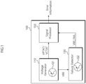
- FIG. 1 is a block diagram illustrating a semiconductor device including a failure detector according to some embodiments of the present disclosure.
- a semiconductor device 100 of the present disclosure may include a voltage generator 110, a failure detector 130, and a signal processor 150.
- the voltage generator 110 may generate a voltage that decreases or increases with temperature.
- the voltage generator 110 may be configured to generate a temperature-complementary voltage VCTAT that decreases with increasing temperature.
- the voltage generator 110 may be configured to generate a temperature-proportional voltage VPTAT that increases with increasing temperature.
- the voltage generator 110 may include a bipolar junction transistor Q1.
- the base-emitter voltage VBE of the bipolar junction transistor Q1 has a complementary to absolute temperature CTAT characteristic that decreases with an increase in temperature.
- the voltage generator 110 may generate the temperature complementary voltage VCTAT or the temperature proportional voltage VPTAT using the base-emitter voltage VBE of the bipolar junction transistor Q1.
- the voltage generator 110 may generate both the temperature complementary voltage VCTAT and the temperature proportional voltage VPTAT based on the base-emitter voltage VBE of the bipolar junction transistor Q1, and may generate, using both of the VPTAT and VCTAT, a voltage that is not significantly affected by temperature.
- the voltage generator 110 has been described with respect to one way to generate a voltage containing temperature information, but the present disclosure is not limited thereto.
- the voltage generator 110 may be any device, circuit, sensor, detector, intellectual property IP block, system-on-chip SoC, application processor AP, or the like that generates the base-emitter voltage VBE of the bipolar junction transistor Q1. That is, the voltage generator 110 may be any device including the bipolar junction transistor Q1.
- the failure detector 130 may monitor the base-emitter voltage VBE of the bipolar junction transistor Q1 generated by the voltage generator 110 to determine whether there is a failure.
- the failure detector 130 may include a bipolar junction transistor Q2 that operates under the same structure and the same conditions as that of the bipolar junction transistor Q1.
- the failure detector 130 may determine whether the base-emitter voltage VBE of the bipolar junction transistor Q1 is abnormal by using the reference voltage generated through the bipolar junction transistor Q2. For example, the failure detector 130 may generate an upper limit reference voltage VBE_UP_REF and a lower limit reference voltage VBE_DN_REF by using the base-emitter voltage VBE of the bipolar junction transistor Q2.
- the failure detector 130 may generate a failure signal VBE_FAIL when the base-emitter voltage VBE of the bipolar junction transistor Q1 is out of the range of the upper limit reference voltage VBE_UP_REF and the lower limit reference voltage VBE_DN_REF.
- the upper limit reference voltage VBE_UP_REF and the lower limit reference voltage VBE_DN_REF change according to temperature with the same slope as the base-emitter voltage VBE. Accordingly, it may be possible to solve a problem that occurs when the failure of the bipolar junction transistor Q1 is determined using a reference voltage that does not change according to the temperature.
- the signal processor 150 may generate information and/or perform a stability operation using at least one of the temperature complementary voltage VCTAT, the temperature proportional voltage VPTAT, and the base-emitter voltage VBE provided from the voltage generator 110.
- the signal processor 150 may sense the temperature using the temperature proportional voltage VPTAT.
- the signal processor 150 may detect a point in time when a specific temperature is reached by using the temperature proportional voltage VPTAT.
- the bipolar junction transistor Q1 of the voltage generator 110 fails, the temperature complementary voltage VCTAT or the temperature proportional voltage VPTAT provided from the voltage generator 110 may become unreliable. Accordingly, when the failure signal VBE_FAIL is provided, the signal processor 150 may be configured to recognize that an error exists in the temperature complementary voltage VCTAT or the temperature proportional voltage VPTAT, and can output error information.
- the semiconductor device 100 may detect the failure of the bipolar junction transistor Q1 by using a reference voltage that changes according to temperature with the same slope as the base-emitter voltage VBE.
- a reference voltage that does not reflect changes in temperature there may be a problem in that an excessively large margin must be used for the upper and lower reference voltages. Accordingly, a failure occurring in the bipolar junction transistor Q1 may not be detected when the excessively large margin is used. This may become a fatal problem in the case of semiconductors or systems for vehicles.
- the present disclosure uses the upper limit reference voltage VBE_UP_REF and the lower limit reference voltage VBE_DN_REF that can reflect the change in temperature. Accordingly, it may be possible to use a relatively narrow margin, so that high reliability failure detection of the bipolar junction transistor Q1 is achievable.
- FIG. 2 is a circuit diagram showing a failure detector according to some embodiments of the present disclosure.
- the failure detector 130 monitors the base-emitter voltage VBE using the upper limit reference voltage VBE_UP_REF and the lower limit reference voltage VBE_DN_REF that vary according to temperature.
- the voltage generator 110 may generate a temperature proportional voltage VPTAT using the base-emitter voltage VBE of the bipolar junction transistor Q1.
- the voltage generator 110 may include a current source 111, the bipolar junction transistor Q1, and an operational amplifier 113.
- a bias current I B may be provided to the diode-connected bipolar junction transistor Q1 by a power supply voltage VDD and the current source 111.
- the base B and the collector C of the bipolar junction transistor Q1 are both grounded. Then, the base-emitter voltage VBE having a magnitude corresponding to the threshold voltage during forward bias may be formed at the emitter terminal of the bipolar junction transistor Q1.
- the base-emitter voltage VBE of the bipolar junction transistor Q1 has a complementary temperature characteristic that decreases as the temperature increases. Accordingly, the resistors R1 and R2 providing negative gain (-R2/R1) and the operational amplifier 113 may be used to generate the temperature proportional voltage VPTAT.
- the failure detector 130 may include a current source 131 configured to provide a current having the same magnitude as the bias current I B of the voltage generator 110.
- the failure detector 130 may include a bipolar junction transistor Q2, resistors R3, R4, and R5 for voltage division, and comparators 133 and 135.
- a bias current I B having the same level as the bias current I B of the voltage generator 110 may be provided to the diode-connected bipolar junction transistor Q2 by the power supply voltage VDD and the current source 131.
- the base B and the collector C of the bipolar junction transistor Q2 are both grounded.
- the base-emitter voltage VBE formed at the emitter terminal of the bipolar junction transistor Q2 is theoretically the same level as the base-emitter voltage VBE of the bipolar junction transistor Q1.
- a resistor R3 is connected between the emitter terminal E and the current source 131. Resistors R4 and R5 connected in series are inserted between the emitter terminal E and the ground.
- the upper limit reference voltage VBE_UP_REF may be provided as a sum of the base-emitter voltage VBE and the voltage 'R3 ⁇ I B ' that is formed in the resistor R3 by the bias current I B .
- the upper limit reference voltage VBE_UP_REF may be expressed as in Equation 1 below.
- VBE _ UP _ REF VBE + R 3 ⁇ I B
- the lower limit reference voltage VBE_DN_REF may be provided as a voltage VBE ⁇ [R5/(R4+R5)] in which the base-emitter voltage VBE is divided by the series resistors R4 and R5. That is, the lower limit reference voltage VBE_DN_REF may be expressed as in Equation 2 below.
- VBE _ DN _ REF VBE ⁇ R 5 R 4 + R 5
- the first comparator 133 may compare the upper limit reference voltage VBE_UP_REF with the base-emitter voltage VBE. If the base-emitter voltage VBE becomes higher than the upper limit reference voltage VBE_UP_REF, the first comparator 133 may activate the first failure signal VBE_FAIL1 and/or set the output of the first comparator 133 to a high level 'H'. On the other hand, when the base-emitter voltage VBE is equal to or lower than the upper limit reference voltage VBE_UP_REF, the first comparator 133 may inactivate the first failure signal VBE_FAIL1 and/or set the output of the first comparator 133 to a low level 'L'.
- the base-emitter voltage VBE may be input to the positive input terminal (+) of the first comparator 133 and the upper limit reference voltage VBE_UP_REF may be input to the negative input terminal (-) of the first comparator 133.
- the second comparator 135 may compare the lower limit reference voltage VBE_DN_REF with the base-emitter voltage VBE. If the base-emitter voltage VBE is lower than the lower limit reference voltage VBE DN REF, the second comparator 135 may activate the second failure signal VBE_FAIL2 and/or set the output of the second comparator 135 to the high level 'H'. On the other hand, when the base-emitter voltage VBE is equal to or higher than the lower limit reference voltage VBE_DN_REF, the second comparator 135 may inactivate the second failure signal VBE_FAIL2 and/or set the output of the second comparator 135 to the low level 'L'.
- the base-emitter voltage VBE is input to the negative input terminal (-) of the second comparator 135 and the lower limit reference voltage VBE_DN_REF is input to the positive input terminal (+) of the second comparator 135.
- the upper limit reference voltage VBE_UP_REF and the lower limit reference voltage VBE_DN_REF based on the base-emitter voltage VBE vary according to temperature. That is, the upper limit reference voltage VBE_UP_REF and the lower limit reference voltage VBE_DN_REF may increase or decrease at the same temperature change rate (or slope) as the base-emitter voltage VBE. In particular, the upper limit reference voltage VBE_UP_REF and the lower limit reference voltage VBE_DN_REF may have a similar tendency to decrease as the temperature increases as the base-emitter voltage VBE, which also decreases as the temperature increases.
- the sizes of the upper limit reference voltage VBE_UP_REF and the lower limit reference voltage VBE_DN_REF may be freely adjusted by adjusting the resistance of the resistors R3, R4, and R5. Since the upper limit reference voltage VBE_UP_REF and the lower limit reference voltage VBE_DN_REF have the same temperature change rate (or slope) as the base-emitter voltage VBE, the upper limit reference voltage VBE_UP_REF and the lower limit reference voltage VBE_DN_REF may be set with a small or relatively smaller detection margin. Accordingly, a failure of the base-emitter voltage VBE can be detected with high or relatively increased reliability with respect to a change in temperature.
- PNP-type bipolar junction transistors Q1 and Q2 are shown in FIG. 2 and have been described with respect to example embodiments in explaining the advantages of the present inventive concepts.
- the present inventive concepts are not limited to the disclosure herein and various modifications are possible. That is, although the bipolar junction transistors Q1 and Q2 of the present disclosure have been described as an example of a PNP type generally used in a CMOS semiconductor process, it will be well understood that they may be NPN type bipolar junction transistors.
- FIG. 3 is a graph illustrating changes according to temperature of the base-emitter voltage VBE, the upper limit reference voltage VBE_UP_REF, and the lower limit reference voltage VBE_DN_REF of FIG. 2 .
- the upper limit reference voltage VBE_UP_REF and the lower limit reference voltage VBE_DN_REF may have the same rate of change with respect to temperature as the base-emitter voltage VBE.
- the upper limit reference voltage VBE_UP_REF may be set higher than the base-emitter voltage VBE by the first offset voltage ⁇ V1 over the entire temperature range as described in Equation 1 above.
- the upper limit reference voltage VBE_UP_REF may have a magnitude 'VBE+ ⁇ V1' obtained by adding the base-emitter voltage VBE to the first offset voltage ⁇ V1 formed in the resistor R3 by the bias current I B .
- the lower limit reference voltage VBE_DN_REF may be set lower than the base-emitter voltage VBE by the second offset voltage ⁇ V2 over the entire temperature range as expressed in Equation 2 above.
- the lower limit reference voltage VBE_DN_REF may have a magnitude 'VBE ⁇ [R5/(R4+R5)]' in which the base-emitter voltage VBE is divided by the series resistors R4 and R5. That is, the lower limit reference voltage VBE_DN_REF with respect to the temperature axis may be expressed as 'VBE- ⁇ V2'.
- the first offset voltage ⁇ V1 and the second offset voltage ⁇ V2 may be set identically or may be set differently.
- the base-emitter voltage VBE has a magnitude of 'V1'. Then, at the same temperature T1, the upper limit reference voltage VBE_UP_REF may be generated with a magnitude of 'V1+ ⁇ V1'. Similarly, at the same temperature T1, the lower limit reference voltage VBE_DN_REF may be generated with a magnitude of'V1- ⁇ V2'.
- the upper limit reference voltage VBE_UP_REF and the lower limit reference voltage VBE_DN_REF are set to 120% and 80% of the base-emitter voltage VBE, respectively.
- the first offset voltage ⁇ V1 that determines the level of the upper limit reference voltage VBE_UP_REF may be 20% of the base-emitter voltage VBE by selecting the bias current I B and the resistor R3.
- the second offset voltage ⁇ V2 that determines the level of the lower limit reference voltage VBE_DN_REF may be 20% of the base-emitter voltage by adjusting the ratio of the series resistors R4 and R5 for voltage division.
- a fixed upper limit reference voltage VBE_UP_REF' and a fixed lower limit reference voltage VBE_DN_REF' that do not change with temperature are also shown in FIG. 3 for comparison. In this case, sufficient margin must be provided to detect the failure of the base-emitter voltage VBE over the entire temperature range.
- the fixed upper limit reference voltage VBE_UP_REF' must have an offset ⁇ V1' that is much larger than the first offset voltage ⁇ V1.
- the fixed lower limit reference voltage VBE_DN_REF must also have an offset ⁇ V2' that is much larger than the second offset voltage ⁇ V2.
- the upper limit reference voltage VBE_UP_REF and the lower limit reference voltage VBE_DN_REF of the present inventive concepts can more freely and/or more uniformly set the offset voltages ⁇ V1 and ⁇ V2 over the entire temperature range. For more precise failure detection, the magnitudes of the offset voltages ⁇ V1 and ⁇ V2 may be further reduced.
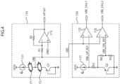
- FIG. 4 is a circuit diagram schematically showing examples of failure of a bipolar junction transistor according to some embodiments of the present inventive concepts. Referring to FIG. 4 , wire disconnection failures F1 and F2 that may occur in the bipolar junction transistor Q1 providing the base-emitter voltage VBE of the voltage generator 110 are illustrated as an example of a failure.
- the supply of the bias current I B to the bipolar junction transistor Q1 may be cut off. Accordingly, the base-emitter voltage VBE formed at the emitter E node of the bipolar junction transistor Q1 will drop without maintaining a fixed value.
- the second disconnection failure F2 occurs, the supply of current to the bipolar junction transistor Q1 may be cut off, but the power supply voltage VDD and the bias current I B at the node to which the base-emitter voltage VBE is output is maintained. Accordingly, the base-emitter voltage VBE will rise rapidly.
- the bipolar junction transistor Q2 of the failure detector 130 will operate normally.
- the upper limit reference voltage VBE_UP_REF and the lower limit reference voltage VBE_DN_REF may be generated based on the normally generated base-emitter voltage VBE of the bipolar junction transistor Q2 of the failure detector 130.
- the base-emitter voltage VBE of Q1 will drop sharply and become lower than the lower limit reference voltage VBE_DN_REF.
- the first failure signal VBE_FAIL1 output by the first comparator 133 will maintain a low level, and the second failure signal VBE_FAIL2 output by the second comparator 135 will transition to a high level.
- the base-emitter voltage VBE of Q1 rapidly rises and becomes higher than the upper limit reference voltage VBE_UP_REF.
- the first failure signal VBE_FAIL1 output by the first comparator 133 will transition to a high level, and the second failure signal VBE _F AIL2 output by the second comparator 135 will maintain a low level.
- the operation of the failure detector 130 when the wire disconnection failures F1 and F2 of the bipolar junction transistor Q1 occurred has been described as an example.
- the types of failure of the bipolar junction transistor Q1 of the voltage generator 110 are not limited to the above-described examples.
- Various types of initial defects or progressive defects or failures may occur in the bipolar junction transistor Q1.
- the failure detector 130 of the present inventive concepts may enable high-reliability failure detection for the bipolar junction transistor Q1 by providing the upper limit reference voltage VBE_UP_REF and the lower limit reference voltage VBE_DN_REF that vary according to temperature.
- FIG. 5 is a timing diagram illustrating a failure detection process of a failure detector in the case of the first disconnection failure F1 of FIG. 4 .
- the base-emitter voltage VBE, the upper limit reference voltage VBE_UP_REF, the lower limit reference voltage VBE_DN_REF, and the first failure signal VBE_FAIL1 and the second failure signal VBE_FAIL2 are shown for a case of the first disconnection failure F1 in which the supply of the bias current I B is cut off.
- the base-emitter voltage VBE may maintain constant offsets ⁇ V1 and ⁇ V2 with the upper limit reference voltage VBE_UP_REF and the lower limit reference voltage VBE_DN_REF. Accordingly, both the first failure signal VBE_FAIL1 output by the first comparator 133 and the second failure signal VBE_FAIL2 output by the second comparator 135 are maintained at the low level 'L'.
- the base-emitter voltage VBE will drop.
- the base-emitter voltage VBE of the bipolar junction transistor Q1 will be lower than the lower limit reference voltage VBE_DN_REF.
- the first failure signal VBE_FAIL1 output by the first comparator 133 may maintain the low level 'L', and the second failure signal VBE FAIL2 output by the second comparator 135 transitions to the high level 'H'.
- the signal processor 150 may detect the second failure signal VBE_FAIL2 and may recognize that a problem has occurred in the base-emitter voltage VBE of the voltage generator 110. In addition, the signal processor 150 may stop using the temperature complementary voltage VCTAT or the temperature proportional voltage VPTAT provided from the voltage generator 110 and may output error information to an external destination.
- FIG. 6 is a timing diagram exemplarily illustrating a failure detection process of a failure detector in the case of the second disconnection failure F2 of FIG. 4 .
- the base-emitter voltage VBE, the upper limit reference voltage VBE_UP_REF and the lower limit reference voltage VBE_DN_REF, and the first failure signal VBE_FAIL1 and the second failure signal VBE _FAIL2 are shown for a case of the second disconnection failure F2.
- the base-emitter voltage VBE may maintain constant offsets ⁇ V1 and ⁇ V2 with the upper limit reference voltage VBE_UP_REF and the lower limit reference voltage VBE_DN_REF, respectively. Accordingly, both the first failure signal VBE_FAIL1 output by the first comparator 133 and the second failure signal VBE_FAIL2 output by the second comparator 135 may be maintained at a low level 'L'.
- the base-emitter voltage VBE may rise rapidly.
- the base-emitter voltage VBE may become higher than the upper limit reference voltage VBE_UP_REF. Then, the first failure signal VBE_FAIL1 output by the first comparator 133 may transition to the high level 'H', and the second failure signal VBE_FAIL2 output by the second comparator 135 may maintain the low level 'L'.
- the signal processor 150 may detect the transition of the first failure signal VBE_FAIL1 and may recognize that a problem has occurred in the base-emitter voltage VBE of the voltage generator 110. In addition, the signal processor 150 may stop using the temperature complementary voltage VCTAT or the temperature proportional voltage VPTAT provided from the voltage generator 110 and may output error information to an external destination.
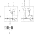
- FIG. 7 is a circuit diagram illustrating another example of a failure of a bipolar junction transistor according to some embodiments of the present disclosure.
- the line width of the line for supplying the bias current I B in the voltage generator 110 may be excessively narrow, so it may be regarded as a narrow width defect F3 that does not supply sufficient current to the bipolar junction transistor Q1.
- the narrow width defect F3 refers to a case in which the line width W2 is excessively narrow compared to the line width W1 of a normal conductive line. In this case, since there is no problem in the operation of the bipolar junction transistor Q1, it may not be detected as a defect during initial production. However, since the current supply to the bipolar junction transistor Q1 is insufficient, it may be difficult to form the base-emitter voltage VBE normally.
- the bipolar junction transistor Q1 When the narrow width defect F3 exists in the conductive line that supplies the bias current I B to the emitter terminal of the bipolar junction transistor Q1, the bipolar junction transistor Q1 may operate normally under normal conditions. However, the linearity of the base-emitter voltage VBE with respect to temperature may be problematic. In this case, as the temperature increases, the base-emitter voltage VBE of the bipolar junction transistor Q1 may not decrease in parallel with the upper limit reference voltage VBE_UP_REF and the lower limit reference voltage VBE_DN_REF. Accordingly, when the operating temperature of the voltage generator 110 increases, the base-emitter voltage VBE may be out of the range of the upper limit reference voltage VBE_UP_REF and the lower limit reference voltage VBE_DN_REF. As a result, the first failure signal VBE_FAIL1 or the second failure signal VBE_FAIL2 may be generated by the failure detector 130.
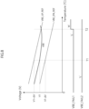
- FIG. 8 is a timing diagram illustrating a failure detection process of a voltage generator in which a narrow width defect F3 of FIG. 7 exists.
- waveforms of signals with respect to the temperature are illustrated in a case when the supply of the bias current I B is not sufficient due to the narrow width defect F3.
- the illustrated signals include a base-emitter voltage VBE, an upper-limit reference voltage VBE_UP_REF and a lower-limit reference voltage VBE_DN_REF, and a first failure signal VBE_FAIL1 and a second failure signal VBE_FAIL2.
- the base-emitter voltage VBE may be normally generated in a temperature range lower than the first temperature T1.
- the slopes with respect to temperature of the base-emitter voltage VBE, the upper-limit reference voltage VBE_UP_REF, and the lower-limit reference voltage VBE_DN_REF are the same. In other words, even if the temperature changes, the base-emitter voltage VBE may not reach the upper limit reference voltage VBE_UP_REF or the lower limit reference voltage VBE_DN_REF.
- the base-emitter voltage VBE may maintain constant offsets ⁇ V1 and ⁇ V2 with the upper limit reference voltage VBE_UP_REF and the lower limit reference voltage VBE_DN_REF, respectively. Accordingly, both the first failure signal VBE_FAIL1 output by the first comparator 133 and the second failure signal VBE_FAIL2 output by the second comparator 135 may be maintained at a low level 'L'.
- the base-emitter voltage VBE of the bipolar junction transistor Q1 may not maintain the offset voltage ⁇ V1 difference as the temperature increases, and may get closer to the upper limit reference voltage VBE_UP_REF. However, in a temperature range lower than the second temperature T2, the base-emitter voltage VBE may remain lower than the upper limit reference voltage VBE_UP_REF. Accordingly, both the first failure signal VBE_FAIL1 output by the first comparator 133 and the second failure signal VBE_FAIL2 output by the second comparator 135 may be maintained at a low level 'L'.
- the base-emitter voltage VBE may be higher than the upper limit reference voltage VBE_UP_REF. Accordingly, the first failure signal VBE_FAIL1 output by the first comparator 133 may transition to the high level 'H'.
- FIG. 9 is a flowchart illustrating a method for detecting a failure of a bipolar junction transistor BJT according to some embodiments of the present disclosure.
- a base-emitter voltage VBE of the bipolar junction transistor BJT e.g., Q1
- reference voltages VBE_UP_REF and VBE_DN_REF of the failure detector 130 may be generated under the same bias conditions.
- high reliability of failure detection of the bipolar junction transistor (BJT) may be possible according to the characteristic that the reference voltages VBE_UP_REF and VBE_DN_REF change with the same slope as the base-emitter voltage VBE with respect to changes in temperature.
- the base-emitter voltage VBE may be generated by the bipolar junction transistor Q1 of the voltage generator 110 (refer to FIG. 2 ).
- the bipolar junction transistor Q1 may use a power supply voltage VDD and the bias current I B .
- the bipolar junction transistor Q1 may have a base terminal B and a collector terminal C grounded for diode connection, and a bias current I B may be supplied to the emitter terminal E.
- a temperature proportional voltage VPTAT or a temperature complementary voltage CTAT may be generated using the generated base-emitter voltage VBE.
- the base-emitter voltage VBE may be generated by the bipolar junction transistor Q2 of the failure detector 130 (refer to FIG. 2 ).
- the bipolar junction transistor Q2 may be provided with the same bias condition as the bipolar junction transistor Q1 of the voltage generator 110. That is, the bipolar junction transistor Q2 may receive the power supply voltage VDD and the bias current I B .
- the base terminal B and the collector terminal C may be grounded for diode connection, and the bias current I B may be supplied to the emitter terminal E.
- an upper limit reference voltage VBE_UP_REF and a lower limit reference voltage VBE_DN_REF may be generated based on the base-emitter voltage VBE generated by the bipolar junction transistor Q2 of the failure detector 130.
- the upper limit reference voltage VBE_UP_REF may be generated using a resistor R3 positioned between the emitter terminal E of the bipolar junction transistor Q2 and the current source 131.
- the lower limit reference voltage VBE_DN_REF may be generated by dividing the base-emitter voltage VBE and voltage dividing resistors R4 and R5, as discussed above.
- step S140 the base-emitter voltage VBE generated by the bipolar junction transistor Q1 may be compared with the upper limit reference voltage VBE_UP_REF and the lower limit reference voltage VBE_DN_REF. If the base-emitter voltage VBE is lower than the upper limit reference voltage VBE_UP_REF and higher than the lower limit reference voltage VBE_DN_REF (or in other words, if the base-emitter voltage VBE is between the upper limit reference voltage VBE_UP_REF and the lower limit reference voltage VBE_DN_REF) ('Yes' direction), the procedure returns to step S 110.
- the procedure moves to step S150.
- step S150 the comparators 133 and 135 (refer to FIG. 2 ) may generate a first failure signal VBE _F AIL 1 or a second failure signal VBE_FAIL2 indicating that the base-emitter voltage VBE is abnormal. Then, the signal processor 150 may generate error information based on the first failure signal VBE_FAIL1 or the second failure signal VBE_FAIL2.
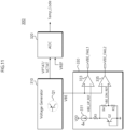
- FIG. 10 is a circuit diagram showing a failure detector of a bipolar junction transistor according to some embodiments of the present disclosure.
- the bipolar junction transistor Q1 of the voltage generator 210 and the bipolar junction transistor Q2 of the failure detector 230 may be connected to respective bias resistors (RB1, RB2).
- the sizes of the bias resistors RB1 and RB2 may be the same or different.
- the voltage generator 210 may generate a temperature proportional voltage VPTAT using the base-emitter voltage VBE of the bipolar junction transistor Q1.
- the voltage generator may include a first bias resistor RB1, a bipolar junction transistor Q1, and an operational amplifier 213.
- a current may be provided to the diode-connected bipolar junction transistor Q1 by the power supply voltage VDD and the first bias resistor RB1.
- the base terminal B and the collector terminal C of the bipolar junction transistor Q1 are both grounded.
- a base-emitter voltage VBE having a magnitude corresponding to the threshold voltage during forward bias may be formed at the emitter terminal E of the bipolar junction transistor Q1.
- a temperature proportional voltage VPTAT may be generated using the base-emitter voltage VBE.
- resistors R1 and R2 providing negative gains '-R2/R1' and the operational amplifier 213 may be used.
- the failure detector 230 may include a second bias resistor RB2, a bipolar junction transistor Q2, resistors R3, R4, and R5, and comparators 233 and 235.
- the base terminal B and the collector terminal C of the bipolar junction transistor Q2 are both grounded.
- the base-emitter voltage VBE formed at the emitter terminal E of the bipolar junction transistor Q2 is theoretically the same as that of the bipolar junction transistor Q1.
- a resistor R3 may be connected between the emitter terminal E and the second bias resistor RB2. Resistors R4 and R5 connected in series are inserted between the emitter terminal E and ground.
- the upper limit reference voltage VBE_UP_REF and the lower limit reference voltage VBE_DN_REF may be generated as discussed above with respect to Equations 1 and 2.
- the first comparator 233 may compare the upper limit reference voltage VBE_UP_REF with the base-emitter voltage VBE. If the base-emitter voltage VBE becomes higher than the upper limit reference voltage VBE_UP_REF, the first comparator 233 may activate the first failure signal VBE_FAIL1 and/or may output the high level 'H'. On the other hand, when the base-emitter voltage VBE is equal to or lower than the upper limit reference voltage VBE_UP_REF, the first comparator 233 may inactivate the first failure signal VBE_FAIL1 and/or may output the low level 'L'.
- the second comparator 235 compares the lower limit reference voltage VBE_DN_REF with the base-emitter voltage VBE. If the base-emitter voltage VBE is lower than the lower limit reference voltage VBE_DN_REF, the second comparator 235 may activate the second failure signal VBE_FAIL2 and/or may output the high level 'H'. On the other hand, when the base-emitter voltage VBE is equal to or higher than the lower limit reference voltage VBE_DN_REF, the second comparator 235 may inactivate the second failure signal VBE _FAIL2 and/or may output the low level 'L'.
- the bipolar junction transistor Q1 of the voltage generator 210 and the bipolar junction transistor Q2 of the failure detector 230 may use bias resistors RB1 and RB2 instead of current sources.
- the bipolar junction transistor Q1 of the voltage generator 210 and the bipolar junction transistor Q2 of the failure detector 230 may be biased in various ways. Bias conditions for generating the base-emitter voltage VBE of the same magnitude may be provided to each of the bipolar junction transistors Q1 and Q2.
- FIG. 11 is a block diagram illustrating a temperature sensor including a failure detector according to some embodiments of the present disclosure.
- a temperature sensor 300 of the present disclosure may include a voltage generator 310, an analog-to-digital converter ADC 320, and a failure detector 330.
- the voltage generator 310 may generate a voltage that decreases or increases with temperature.
- the voltage generator 310 may be configured to generate a temperature complementary voltage VCTAT whose voltage decrease with increasing temperature.
- the voltage generator 310 may be configured to generate a temperature proportional voltage VPTAT whose voltage increases with increasing temperature.
- the voltage generator 310 may include a bipolar junction transistor Q1.
- a temperature proportional voltage VPTAT or a temperature complementary voltage VCTAT may be generated using the base-emitter voltage VBE of the bipolar junction transistor Q1.
- the analog-to-digital converter 320 may convert a temperature proportional voltage (VPTAT) or a temperature complementary voltage VCTAT provided as an analog signal into a digital signal indicating temperature information. For example, the analog-to-digital converter 320 may compare the temperature proportional voltage VPTAT or the temperature complementary voltage VCTAT with the reference voltage VREF and generate or convert the temperature code Temp_Code. The analog-to-digital converter 320 may output current temperature value to an external destination through the temperature code Temp_Code.
- VTAT temperature proportional voltage
- VCTAT temperature complementary voltage
- the analog-to-digital converter 320 may output current temperature value to an external destination through the temperature code Temp_Code.
- the failure detector 330 may monitor the base-emitter voltage VBE of the bipolar junction transistor Q1 generated by the voltage generator 310 and may determine whether the bipolar junction transistor Q1 has failed. To this end, the failure detector 330 may include a bipolar junction transistor Q2 having the same structure as the bipolar junction transistor Q1 and operating under the same bias condition. The failure detector 330 may determine whether the base-emitter voltage VBE of the bipolar junction transistor Q1 is abnormal by using the reference voltage generated through the bipolar junction transistor Q2.
- the failure detector 330 may generate an upper limit reference voltage VBE_UP_REF and a lower limit reference voltage VBE_DN_REF by using the base-emitter voltage VBE of the bipolar junction transistor Q2.
- the failure detector 330 may generate failure signals VBE_FAIL1 and VBE_FAIL2 when the base-emitter voltage VBE of the bipolar junction transistor Q1 is out of the range of the upper limit reference voltage VBE_UP_REF and the lower limit reference voltage VBE_DN_REF.
- the failure detector 330 may include a current source 331 and the bipolar junction transistor Q2 of substantially the same size as the bipolar junction transistor Q1 included in the voltage generator 310.
- the failure detector 330 may include resistors R3, R4, R5 and comparators 333 and 335.
- a bias current I B may be provided to the diode-connected bipolar junction transistor Q2 by a power supply voltage VDD and a current source 331 of the same level as that of the voltage generator 310.
- the base terminal B and the collector terminal C of the bipolar junction transistor Q2 may both be grounded.
- the base-emitter voltage VBE formed at the emitter terminal E of the bipolar junction transistor Q2 is theoretically the same as that of the bipolar junction transistor Q1 of the voltage generator 310.
- the generating mechanism of the upper limit reference voltage VBE_UP_REF and the lower limit reference voltage VBE_DN_REF may be substantially the same as that described in FIG. 2 .
- a method of generating the first failure signal VBE_FAIL1 and the second failure signal VBE_FAIL2 using the first comparator 333 and the second comparator 335 may be substantially the same as the description of FIG. 2 . Therefore, descriptions thereof will be omitted here in the interest of brevity.
- the temperature sensor 300 can detect a failure of the voltage generator 310 for generating the temperature code Temp_Code with high reliability. That is, the failure of the bipolar junction transistor Q1 may be detected using a reference voltage that has the same slope as the base-emitter voltage VBE according to changes in temperature. When using a reference voltage that does not reflect changes in temperature, there may be a problem in that an excessively large margin must be used for the upper and lower reference voltages. Accordingly, a failure occurring in the bipolar junction transistor Q1 may not be detected when an excessively large margin is used. This may become a fatal problem in the case of semiconductors or systems for vehicles and/or directly related to human life.
- the present inventive concepts may use an upper limit reference voltage VBE_UP_REF and a lower limit reference voltage VBE_DN_REF that can reflect changes in temperature. Accordingly, it may be possible to use a relatively narrow margin, so that a high-reliability failure detection for the bipolar junction transistor Q1 is possible.
- FIG. 12 is a block diagram illustrating a temperature detector including a failure detector according to some embodiments of the present inventive concepts.
- a temperature detector 400 of the present disclosure may include a voltage generator 410, a detector 420, and a failure detector 430.
- the voltage generator 410 may generate a voltage that decreases or increases with temperature.
- the voltage generator 410 may be configured to generate a temperature complementary voltage VCTAT or a temperature proportional voltage VPTAT whose voltage varies according to an increase in temperature.
- the voltage generator 410 may include a bipolar junction transistor Q1.
- a temperature proportional voltage VPTAT or a temperature complementary voltage VCTAT may be generated using the base-emitter voltage VBE of the bipolar junction transistor Q1.
- the detector 420 may compare the temperature proportional voltage VPTAT or the temperature complementary voltage VCTAT provided as an analog signal with the reference voltage VREF to detect whether a specific temperature is reached.
- the reference voltage VREF may be provided as a voltage corresponding to a target temperature.
- the detector 420 may generate a flag signal Flag when the temperature proportional voltage VPTAT or the temperature complementary voltage VCTAT reaches the reference voltage VREF.
- the failure detector 430 may monitor the base-emitter voltage VBE of the bipolar junction transistor Q1 generated by the voltage generator 410 to determine whether the bipolar junction transistor Q1 has failed.
- the failure detector 430 may include a bipolar junction transistor Q2 that operates under the same structure and conditions as that of the bipolar junction transistor Q1.
- the failure detector 430 may determine whether the base-emitter voltage VBE of the bipolar junction transistor Q1 is abnormal by using the reference voltage generated through the bipolar junction transistor Q2.
- the failure detector 430 may include a current source 431 and the bipolar junction transistor Q2 of substantially the same size as the bipolar junction transistor Q1 included in the voltage generator 410.
- the failure detector 430 may include resistors R3, R4, R5 and comparators 433 and 435.
- a bias current I B may be provided to the diode-connected bipolar junction transistor Q2 by a power supply voltage VDD and a current source 431 of the same level as that of the voltage generator 410.
- the operating mechanism of the failure detector 430 may be substantially the same as that described in FIG. 2 .
- a method of generating the first failure signal VBE_FAIL1 and the second failure signal VBE_FAIL2 using the first comparator 433 and the second comparator 435 may be substantially the same as the description of FIG. 2 . Therefore, descriptions thereof will be omitted here in the interest of brevity.
- the failure of the voltage generator 410 including the bipolar junction transistor Q1 can be detected with high reliability.
- FIG. 13 is a block diagram illustrating a vehicle semiconductor device 500 including a failure detector according to some embodiments of the present disclosure.
- a semiconductor device 500 for a vehicle according to the present disclosure may include a voltage generator 510, a micro control unit MCU 520, and a failure detector 530.
- the voltage generator 510 may generate a voltage Vtemp that includes temperature information.
- the voltage generator 510 may be configured to generate a temperature complementary voltage VCTAT or a temperature proportional voltage VPTAT including temperature information.
- the voltage generator 510 may include a bipolar junction transistor Q1.
- a temperature proportional voltage VPTAT or a temperature complementary voltage VCTAT may be generated using the base-emitter voltage VBE of the bipolar junction transistor Q1.
- the MCU 520 may use a voltage Vtemp including temperature information to adjust a driving system or a sensor of the vehicle.
- the MCU 520 may control the air conditioner or drivers of the vehicle using the voltage Vtemp including the temperature information.
- the failure detector 530 may monitor the base-emitter voltage VBE of the bipolar junction transistor Q1 generated by the voltage generator 510 to determine whether the bipolar junction transistor Q1 has failed.
- the failure detector 530 may include a bipolar junction transistor Q2 operating under the same structure and conditions as that of the bipolar junction transistor Q1.
- the failure detector 530 may determine whether the base-emitter voltage VBE of the bipolar junction transistor Q1 is abnormal by using the reference voltage generated through the bipolar junction transistor Q2.
- the failure detector 530 may include a current source 531 and the bipolar junction transistor Q2 of substantially the same size as the bipolar junction transistor Q1 included in the voltage generator 510.
- the failure detector 530 may include resistors R3, R4, and R5, comparators 533 and 535, and an OR gate 537.
- a bias current I B may be provided to the diode-connected bipolar junction transistor Q2 by a power supply voltage VDD and a current source 531 of the same level as that of the voltage generator 510.
- the base terminal B and the collector terminal C of the bipolar junction transistor Q2 may both be grounded.
- the base-emitter voltage VBE formed at the emitter terminal E of the bipolar junction transistor Q2 is theoretically the same as that of the bipolar junction transistor Q1 of the voltage generator 510.
- the generating mechanism of the upper limit reference voltage VBE_UP_REF and the lower limit reference voltage VBE_DN_REF may be substantially the same as that described in FIG. 2 .
- a method of generating the first failure signal VBE_FAIL1 and the second failure signal VBE_FAIL2 using the first comparator 533 and the second comparator 535 may be substantially the same as the description of FIG. 2 . Therefore, descriptions thereof will be omitted here in the interest of brevity.
- first failure signal VBE _F AIL 1 and the second failure signal VBE_FAIL2 may be processed by the OR gate 537 and generated as the failure signal VBE_FAIL.
- the failure signal VBE_FAIL may be used for operation control by the MCU 520.
- the failure detector 530 can detect the failure of the voltage generator 510 including the bipolar junction transistor Q1 with high reliability.
- the present inventive concepts may include simple design changes or easily changeable embodiments.
- the present inventive concepts will include techniques that can be easily modified and implemented using the embodiments. Therefore, the scope of the present inventive concepts should not be limited to the above-described embodiments, and should be defined by the claims.
Landscapes
- Physics & Mathematics (AREA)
- General Physics & Mathematics (AREA)
- Engineering & Computer Science (AREA)
- Microelectronics & Electronic Packaging (AREA)
- Measuring Temperature Or Quantity Of Heat (AREA)
- Logic Circuits (AREA)
- Testing Or Measuring Of Semiconductors Or The Like (AREA)
- Bipolar Integrated Circuits (AREA)
- Amplifiers (AREA)
Abstract
Description
- Aspects of the inventive concepts relate to semiconductor devices, and more particularly, to semiconductor devices that include a detector for detecting an error or a failure of a bipolar junction transistor, and to methods for detecting a failure of a bipolar junction transistor.
- Due to the development of fine processes, it may be possible to integrate more devices per unit area in a semiconductor chip. In addition, performance improvement of semiconductor chips is also accelerating. Due to improved performance and reduced line width, heat generated in a semiconductor device has a great influence on device stability. In particular, when a semiconductor device used in an electric system of a vehicle malfunctions due to factors such as voltage, current, and temperature, it may affect directly the life, comfort, and/or well-being of a driver. Accordingly, research on temperature management systems for ensuring the stability of the semiconductor device is being actively conducted.
- A temperature sensor, which is a core component of a temperature management system, is generally implemented using a bipolar junction transistor BJT. More specifically, conventional bipolar junction transistor BJT based temperature sensors may sense the temperature using the emitter-base voltage VEB difference that varies according to the ratio of the amount of current flowing through the two BJTs.
- In semiconductor devices using the bipolar junction transistor (BJT) as detectors or sensors, there are not many means for identifying the failure of the bipolar junction transistor BJT. A reference voltage is required to monitor whether the emitter-base voltage VEB of the bipolar junction transistor BJT is abnormal. In general, it is possible to determine whether the emitter-base voltage VEB is abnormal using a band-gap reference BGR. However, when monitoring the temperature-varying emitter-base voltage VEB using a fixed reference voltage, a large margin with respect to temperature must be considered. If a reference voltage with a large margin for temperature is used, the reliability of failure detection is inevitably lowered. For this reason, failure detection technology having high reliability even in the temperature change of the bipolar junction transistor BJT is being pursued.
- Some aspects of the present disclosure provides failure detectors and failure detection methods in semiconductor devices using a base-emitter voltage of bipolar junction transistor BJT that varies with temperature as a reference.
- According to some embodiments of the inventive concept, a semiconductor device may include a voltage generator configured to generate a first base-emitter voltage of a first bipolar junction transistor, and a failure detector configured to generate a failure signal by comparing the first base-emitter voltage with an upper limit reference voltage and a lower limit reference voltage. The failure detector may include: a second bipolar junction transistor in which a base terminal and a collector terminal are grounded, a current source configured to generate a bias current, a first resistor coupled between the current source and an emitter terminal of the second bipolar junction transistor to generate the upper limit reference voltage, a second resistor and a third resistor configured to divide a second base-emitter voltage of the second bipolar junction transistor to generate the lower limit reference voltage, a first comparator configured to compare the first base-emitter voltage with the upper limit reference voltage and configured to generate a first failure signal, and a second comparator configured to compare the first base-emitter voltage with the lower limit reference voltage and configured to generate a second failure signal.
- According to some embodiments of the inventive concepts, a semiconductor device may include a first bipolar junction transistor configured to generate a first base-emitter voltage, a second bipolar junction transistor configured to generate a second base-emitter voltage, a reference generator configured to generate at least one reference voltage based on the second base-emitter voltage, and a comparator configured to compare the generated at least one reference voltage and the first base-emitter voltage and generate a failure signal based on the comparison.
- According to some embodiments of the inventive concepts, a method for detecting a failure in a semiconductor device using a bipolar junction transistor may include generating a first base-emitter voltage from a first bipolar junction transistor, generating a second base-emitter voltage from a second bipolar junction transistor, generating an upper limit reference voltage and a lower limit reference voltage from the second base-emitter voltage, and determining a failure of the first bipolar junction transistor by comparing the first base-emitter voltage with the upper limit reference voltage or the lower limit reference voltage.
- The above and other objects and features of the present disclosure will become apparent by describing in detail embodiments thereof with reference to the accompanying drawings.
-
FIG. 1 is a block diagram illustrating a semiconductor device including a failure detector according to an embodiment of the present disclosure. -
FIG. 2 is a circuit diagram showing a failure detector according to an embodiment of the present disclosure. -
FIG. 3 is a graph exemplarily showing changes according to temperature of the base-emitter voltage VBE, the upper limit reference voltage VBE_UP_REF, and the lower limit reference voltage VBE_DN_REF ofFIG. 2 . -
FIG. 4 is a circuit diagram schematically showing examples of failure of a bipolar junction transistor according to an embodiment of the present disclosure. -
FIG. 5 is a timing diagram exemplarily illustrating a failure detection process of a failure detector in the case of the first disconnection failure F1 ofFIG. 4 . -
FIG. 6 is a timing diagram exemplarily illustrating a failure detection process of a failure detector in the case of the second disconnection failure F2 ofFIG. 4 . -
FIG. 7 is a circuit diagram illustrating another example of a failure of a bipolar junction transistor according to an embodiment of the present disclosure. -
FIG. 8 is a timing diagram exemplarily illustrating a failure detection process of a voltage generator in which a narrow line width defect F3 is present inFIG. 7 . -
FIG. 9 is a flowchart illustrating a method for detecting a failure of a bipolar junction transistor (BJT) according to an embodiment of the present disclosure. -
FIG. 10 is a circuit diagram showing a failure detector of a bipolar junction transistor according to another embodiment of the present disclosure. -
FIG. 11 is a block diagram illustrating a temperature sensor including a failure detector according to an embodiment of the present disclosure. -
FIG. 12 is a block diagram illustrating a temperature detector including a failure detector according to an embodiment of the present disclosure. -
FIG. 13 is a block diagram illustrating avehicle semiconductor device 500 including a failure detector according to an embodiment of the present disclosure. - It is to be understood that both the foregoing brief summary and the following detailed description are merely examples, and it is to be considered that additional description of the inventive concepts is provided herein. Reference signs are indicated in detail in preferred embodiments of the present inventive concepts, examples of which are indicated in the reference drawings. Wherever possible, the same reference numbers are used in the description and drawings to refer to the same or like parts.
- In the following, the advantages of the present inventive concepts will be described with examples of sensors and/or detectors using a bipolar junction transistor (BJT). However, those skilled in the art will readily appreciate other advantages and capabilities of the present inventive concepts in accordance with the teachings herein. The present inventive concepts may be implemented or applied through other embodiments. Moreover, the detailed description may be modified or changed without departing significantly from the scope, spirit and other objects of the present inventive concepts.
-
FIG. 1 is a block diagram illustrating a semiconductor device including a failure detector according to some embodiments of the present disclosure. Referring toFIG. 1 , asemiconductor device 100 of the present disclosure may include avoltage generator 110, afailure detector 130, and asignal processor 150. - The
voltage generator 110 may generate a voltage that decreases or increases with temperature. For example, thevoltage generator 110 may be configured to generate a temperature-complementary voltage VCTAT that decreases with increasing temperature. Alternatively, thevoltage generator 110 may be configured to generate a temperature-proportional voltage VPTAT that increases with increasing temperature. Thevoltage generator 110 may include a bipolar junction transistor Q1. In general, the base-emitter voltage VBE of the bipolar junction transistor Q1 has a complementary to absolute temperature CTAT characteristic that decreases with an increase in temperature. Thevoltage generator 110 may generate the temperature complementary voltage VCTAT or the temperature proportional voltage VPTAT using the base-emitter voltage VBE of the bipolar junction transistor Q1. Alternatively, thevoltage generator 110 may generate both the temperature complementary voltage VCTAT and the temperature proportional voltage VPTAT based on the base-emitter voltage VBE of the bipolar junction transistor Q1, and may generate, using both of the VPTAT and VCTAT, a voltage that is not significantly affected by temperature. Here, thevoltage generator 110 has been described with respect to one way to generate a voltage containing temperature information, but the present disclosure is not limited thereto. For example, thevoltage generator 110 may be any device, circuit, sensor, detector, intellectual property IP block, system-on-chip SoC, application processor AP, or the like that generates the base-emitter voltage VBE of the bipolar junction transistor Q1. That is, thevoltage generator 110 may be any device including the bipolar junction transistor Q1. - The
failure detector 130 may monitor the base-emitter voltage VBE of the bipolar junction transistor Q1 generated by thevoltage generator 110 to determine whether there is a failure. Thefailure detector 130 may include a bipolar junction transistor Q2 that operates under the same structure and the same conditions as that of the bipolar junction transistor Q1. Thefailure detector 130 may determine whether the base-emitter voltage VBE of the bipolar junction transistor Q1 is abnormal by using the reference voltage generated through the bipolar junction transistor Q2. For example, thefailure detector 130 may generate an upper limit reference voltage VBE_UP_REF and a lower limit reference voltage VBE_DN_REF by using the base-emitter voltage VBE of the bipolar junction transistor Q2. Thefailure detector 130 may generate a failure signal VBE_FAIL when the base-emitter voltage VBE of the bipolar junction transistor Q1 is out of the range of the upper limit reference voltage VBE_UP_REF and the lower limit reference voltage VBE_DN_REF. The upper limit reference voltage VBE_UP_REF and the lower limit reference voltage VBE_DN_REF change according to temperature with the same slope as the base-emitter voltage VBE. Accordingly, it may be possible to solve a problem that occurs when the failure of the bipolar junction transistor Q1 is determined using a reference voltage that does not change according to the temperature. - The
signal processor 150 may generate information and/or perform a stability operation using at least one of the temperature complementary voltage VCTAT, the temperature proportional voltage VPTAT, and the base-emitter voltage VBE provided from thevoltage generator 110. For example, thesignal processor 150 may sense the temperature using the temperature proportional voltage VPTAT. Alternatively, thesignal processor 150 may detect a point in time when a specific temperature is reached by using the temperature proportional voltage VPTAT. However, when the bipolar junction transistor Q1 of thevoltage generator 110 fails, the temperature complementary voltage VCTAT or the temperature proportional voltage VPTAT provided from thevoltage generator 110 may become unreliable. Accordingly, when the failure signal VBE_FAIL is provided, thesignal processor 150 may be configured to recognize that an error exists in the temperature complementary voltage VCTAT or the temperature proportional voltage VPTAT, and can output error information. - As described above, the
semiconductor device 100 according to some embodiments of the present disclosure may detect the failure of the bipolar junction transistor Q1 by using a reference voltage that changes according to temperature with the same slope as the base-emitter voltage VBE. In contrast, when using a reference voltage that does not reflect changes in temperature, there may be a problem in that an excessively large margin must be used for the upper and lower reference voltages. Accordingly, a failure occurring in the bipolar junction transistor Q1 may not be detected when the excessively large margin is used. This may become a fatal problem in the case of semiconductors or systems for vehicles. The present disclosure uses the upper limit reference voltage VBE_UP_REF and the lower limit reference voltage VBE_DN_REF that can reflect the change in temperature. Accordingly, it may be possible to use a relatively narrow margin, so that high reliability failure detection of the bipolar junction transistor Q1 is achievable. -
FIG. 2 is a circuit diagram showing a failure detector according to some embodiments of the present disclosure. Referring toFIG. 2 , thefailure detector 130 monitors the base-emitter voltage VBE using the upper limit reference voltage VBE_UP_REF and the lower limit reference voltage VBE_DN_REF that vary according to temperature. - The
voltage generator 110 may generate a temperature proportional voltage VPTAT using the base-emitter voltage VBE of the bipolar junction transistor Q1. Thevoltage generator 110 may include acurrent source 111, the bipolar junction transistor Q1, and anoperational amplifier 113. A bias current IB may be provided to the diode-connected bipolar junction transistor Q1 by a power supply voltage VDD and thecurrent source 111. The base B and the collector C of the bipolar junction transistor Q1 are both grounded. Then, the base-emitter voltage VBE having a magnitude corresponding to the threshold voltage during forward bias may be formed at the emitter terminal of the bipolar junction transistor Q1. - The base-emitter voltage VBE of the bipolar junction transistor Q1 has a complementary temperature characteristic that decreases as the temperature increases. Accordingly, the resistors R1 and R2 providing negative gain (-R2/R1) and the
operational amplifier 113 may be used to generate the temperature proportional voltage VPTAT. - The
failure detector 130 may include acurrent source 131 configured to provide a current having the same magnitude as the bias current IB of thevoltage generator 110. Thefailure detector 130 may include a bipolar junction transistor Q2, resistors R3, R4, and R5 for voltage division, andcomparators voltage generator 110 may be provided to the diode-connected bipolar junction transistor Q2 by the power supply voltage VDD and thecurrent source 131. The base B and the collector C of the bipolar junction transistor Q2 are both grounded. The base-emitter voltage VBE formed at the emitter terminal of the bipolar junction transistor Q2 is theoretically the same level as the base-emitter voltage VBE of the bipolar junction transistor Q1. - In order to generate the upper limit reference voltage VBE_UP_REF and the lower limit reference voltage VBE_DN_REF based on the base-emitter voltage VBE, a resistor R3 is connected between the emitter terminal E and the
current source 131. Resistors R4 and R5 connected in series are inserted between the emitter terminal E and the ground. The upper limit reference voltage VBE_UP_REF may be provided as a sum of the base-emitter voltage VBE and the voltage 'R3× IB' that is formed in the resistor R3 by the bias current IB. The upper limit reference voltage VBE_UP_REF may be expressed as in Equation 1 below.
- The lower limit reference voltage VBE_DN_REF may be provided as a voltage VBE×[R5/(R4+R5)] in which the base-emitter voltage VBE is divided by the series resistors R4 and R5. That is, the lower limit reference voltage VBE_DN_REF may be expressed as in Equation 2 below.

- The
first comparator 133 may compare the upper limit reference voltage VBE_UP_REF with the base-emitter voltage VBE. If the base-emitter voltage VBE becomes higher than the upper limit reference voltage VBE_UP_REF, thefirst comparator 133 may activate the first failure signal VBE_FAIL1 and/or set the output of thefirst comparator 133 to a high level 'H'. On the other hand, when the base-emitter voltage VBE is equal to or lower than the upper limit reference voltage VBE_UP_REF, thefirst comparator 133 may inactivate the first failure signal VBE_FAIL1 and/or set the output of thefirst comparator 133 to a low level 'L'. The base-emitter voltage VBE may be input to the positive input terminal (+) of thefirst comparator 133 and the upper limit reference voltage VBE_UP_REF may be input to the negative input terminal (-) of thefirst comparator 133. - The
second comparator 135 may compare the lower limit reference voltage VBE_DN_REF with the base-emitter voltage VBE. If the base-emitter voltage VBE is lower than the lower limit reference voltage VBE DN REF, thesecond comparator 135 may activate the second failure signal VBE_FAIL2 and/or set the output of thesecond comparator 135 to the high level 'H'. On the other hand, when the base-emitter voltage VBE is equal to or higher than the lower limit reference voltage VBE_DN_REF, thesecond comparator 135 may inactivate the second failure signal VBE_FAIL2 and/or set the output of thesecond comparator 135 to the low level 'L'. The base-emitter voltage VBE is input to the negative input terminal (-) of thesecond comparator 135 and the lower limit reference voltage VBE_DN_REF is input to the positive input terminal (+) of thesecond comparator 135. - In the above description, the upper limit reference voltage VBE_UP_REF and the lower limit reference voltage VBE_DN_REF based on the base-emitter voltage VBE vary according to temperature. That is, the upper limit reference voltage VBE_UP_REF and the lower limit reference voltage VBE_DN_REF may increase or decrease at the same temperature change rate (or slope) as the base-emitter voltage VBE. In particular, the upper limit reference voltage VBE_UP_REF and the lower limit reference voltage VBE_DN_REF may have a similar tendency to decrease as the temperature increases as the base-emitter voltage VBE, which also decreases as the temperature increases.
- In addition, the sizes of the upper limit reference voltage VBE_UP_REF and the lower limit reference voltage VBE_DN_REF may be freely adjusted by adjusting the resistance of the resistors R3, R4, and R5. Since the upper limit reference voltage VBE_UP_REF and the lower limit reference voltage VBE_DN_REF have the same temperature change rate (or slope) as the base-emitter voltage VBE, the upper limit reference voltage VBE_UP_REF and the lower limit reference voltage VBE_DN_REF may be set with a small or relatively smaller detection margin. Accordingly, a failure of the base-emitter voltage VBE can be detected with high or relatively increased reliability with respect to a change in temperature.
- PNP-type bipolar junction transistors Q1 and Q2 are shown in
FIG. 2 and have been described with respect to example embodiments in explaining the advantages of the present inventive concepts. However, the present inventive concepts are not limited to the disclosure herein and various modifications are possible. That is, although the bipolar junction transistors Q1 and Q2 of the present disclosure have been described as an example of a PNP type generally used in a CMOS semiconductor process, it will be well understood that they may be NPN type bipolar junction transistors. -
FIG. 3 is a graph illustrating changes according to temperature of the base-emitter voltage VBE, the upper limit reference voltage VBE_UP_REF, and the lower limit reference voltage VBE_DN_REF ofFIG. 2 . Referring toFIG. 3 , the upper limit reference voltage VBE_UP_REF and the lower limit reference voltage VBE_DN_REF may have the same rate of change with respect to temperature as the base-emitter voltage VBE. - The upper limit reference voltage VBE_UP_REF may be set higher than the base-emitter voltage VBE by the first offset voltage ΔV1 over the entire temperature range as described in Equation 1 above. For example, the upper limit reference voltage VBE_UP_REF may have a magnitude 'VBE+ΔV1' obtained by adding the base-emitter voltage VBE to the first offset voltage ΔV1 formed in the resistor R3 by the bias current IB. The lower limit reference voltage VBE_DN_REF may be set lower than the base-emitter voltage VBE by the second offset voltage ΔV2 over the entire temperature range as expressed in Equation 2 above. For example, the lower limit reference voltage VBE_DN_REF may have a magnitude 'VBE×[R5/(R4+R5)]' in which the base-emitter voltage VBE is divided by the series resistors R4 and R5. That is, the lower limit reference voltage VBE_DN_REF with respect to the temperature axis may be expressed as 'VBE-ΔV2'. Here, the first offset voltage ΔV1 and the second offset voltage ΔV2 may be set identically or may be set differently.
- At a specific temperature (e.g., T1), it may be assumed that the base-emitter voltage VBE has a magnitude of 'V1'. Then, at the same temperature T1, the upper limit reference voltage VBE_UP_REF may be generated with a magnitude of 'V1+ΔV1'. Similarly, at the same temperature T1, the lower limit reference voltage VBE_DN_REF may be generated with a magnitude of'V1-ΔV2'.
- It is assumed that the upper limit reference voltage VBE_UP_REF and the lower limit reference voltage VBE_DN_REF are set to 120% and 80% of the base-emitter voltage VBE, respectively. In other words, the first offset voltage ΔV1 that determines the level of the upper limit reference voltage VBE_UP_REF may be 20% of the base-emitter voltage VBE by selecting the bias current IB and the resistor R3. Similarly, the second offset voltage ΔV2 that determines the level of the lower limit reference voltage VBE_DN_REF may be 20% of the base-emitter voltage by adjusting the ratio of the series resistors R4 and R5 for voltage division.
- A fixed upper limit reference voltage VBE_UP_REF' and a fixed lower limit reference voltage VBE_DN_REF' that do not change with temperature are also shown in
FIG. 3 for comparison. In this case, sufficient margin must be provided to detect the failure of the base-emitter voltage VBE over the entire temperature range. At a specific temperature T1, when the base-emitter voltage VBE is 'V1', the fixed upper limit reference voltage VBE_UP_REF' must have an offset ΔV1' that is much larger than the first offset voltage ΔV1. In addition, the fixed lower limit reference voltage VBE_DN_REF must also have an offset ΔV2' that is much larger than the second offset voltage ΔV2. These relatively large offsets ΔV1' and ΔV2' may be factors that deteriorate the precision and reliability of failure detection of the base-emitter voltage VBE. - As seen from comparison with the fixed upper limit reference voltage VBE_UP_REF' and the fixed lower limit reference voltage VBE_DN_REF, the upper limit reference voltage VBE_UP_REF and the lower limit reference voltage VBE_DN_REF of the present inventive concepts can more freely and/or more uniformly set the offset voltages ΔV1 and ΔV2 over the entire temperature range. For more precise failure detection, the magnitudes of the offset voltages ΔV1 and ΔV2 may be further reduced.
-
FIG. 4 is a circuit diagram schematically showing examples of failure of a bipolar junction transistor according to some embodiments of the present inventive concepts. Referring toFIG. 4 , wire disconnection failures F1 and F2 that may occur in the bipolar junction transistor Q1 providing the base-emitter voltage VBE of thevoltage generator 110 are illustrated as an example of a failure. - If the first disconnection failure F1 occurs, the supply of the bias current IB to the bipolar junction transistor Q1 may be cut off. Accordingly, the base-emitter voltage VBE formed at the emitter E node of the bipolar junction transistor Q1 will drop without maintaining a fixed value. On the other hand, when the second disconnection failure F2 occurs, the supply of current to the bipolar junction transistor Q1 may be cut off, but the power supply voltage VDD and the bias current IB at the node to which the base-emitter voltage VBE is output is maintained. Accordingly, the base-emitter voltage VBE will rise rapidly.
- Despite the failure of the bipolar junction transistor Q1, the bipolar junction transistor Q2 of the
failure detector 130 will operate normally. In addition, the upper limit reference voltage VBE_UP_REF and the lower limit reference voltage VBE_DN_REF may be generated based on the normally generated base-emitter voltage VBE of the bipolar junction transistor Q2 of thefailure detector 130. When the first disconnection failure F1 occurs, the base-emitter voltage VBE of Q1 will drop sharply and become lower than the lower limit reference voltage VBE_DN_REF. The first failure signal VBE_FAIL1 output by thefirst comparator 133 will maintain a low level, and the second failure signal VBE_FAIL2 output by thesecond comparator 135 will transition to a high level. On the other hand, when the second disconnection failure F2 occurs, the base-emitter voltage VBE of Q1 rapidly rises and becomes higher than the upper limit reference voltage VBE_UP_REF. The first failure signal VBE_FAIL1 output by thefirst comparator 133 will transition to a high level, and the second failure signal VBE _F AIL2 output by thesecond comparator 135 will maintain a low level. - In the above, the operation of the
failure detector 130 when the wire disconnection failures F1 and F2 of the bipolar junction transistor Q1 occurred has been described as an example. However, the types of failure of the bipolar junction transistor Q1 of thevoltage generator 110 are not limited to the above-described examples. Various types of initial defects or progressive defects or failures may occur in the bipolar junction transistor Q1. Thefailure detector 130 of the present inventive concepts may enable high-reliability failure detection for the bipolar junction transistor Q1 by providing the upper limit reference voltage VBE_UP_REF and the lower limit reference voltage VBE_DN_REF that vary according to temperature. -
FIG. 5 is a timing diagram illustrating a failure detection process of a failure detector in the case of the first disconnection failure F1 ofFIG. 4 . Referring toFIG. 5 , the base-emitter voltage VBE, the upper limit reference voltage VBE_UP_REF, the lower limit reference voltage VBE_DN_REF, and the first failure signal VBE_FAIL1 and the second failure signal VBE_FAIL2 are shown for a case of the first disconnection failure F1 in which the supply of the bias current IB is cut off. - Before 11, which is the time of occurrence of the first disconnection failure F1, the base-emitter voltage VBE may maintain constant offsets ΔV1 and ΔV2 with the upper limit reference voltage VBE_UP_REF and the lower limit reference voltage VBE_DN_REF. Accordingly, both the first failure signal VBE_FAIL1 output by the
first comparator 133 and the second failure signal VBE_FAIL2 output by thesecond comparator 135 are maintained at the low level 'L'. - However, as the supply of the bias current IB to the bipolar junction transistor Q1 is cut off from the time t1 when the first disconnection failure F1 occurs, the base-emitter voltage VBE will drop. At a time t2, the base-emitter voltage VBE of the bipolar junction transistor Q1 will be lower than the lower limit reference voltage VBE_DN_REF. Then, the first failure signal VBE_FAIL1 output by the
first comparator 133 may maintain the low level 'L', and the second failure signal VBE FAIL2 output by thesecond comparator 135 transitions to the high level 'H'. - The signal processor 150 (refer to
FIG. 1 ) may detect the second failure signal VBE_FAIL2 and may recognize that a problem has occurred in the base-emitter voltage VBE of thevoltage generator 110. In addition, thesignal processor 150 may stop using the temperature complementary voltage VCTAT or the temperature proportional voltage VPTAT provided from thevoltage generator 110 and may output error information to an external destination. -
FIG. 6 is a timing diagram exemplarily illustrating a failure detection process of a failure detector in the case of the second disconnection failure F2 ofFIG. 4 . Referring toFIG. 6 , the base-emitter voltage VBE, the upper limit reference voltage VBE_UP_REF and the lower limit reference voltage VBE_DN_REF, and the first failure signal VBE_FAIL1 and the second failure signal VBE _FAIL2 are shown for a case of the second disconnection failure F2. - Before 11, which is the time of occurrence of the second disconnection failure F2, the base-emitter voltage VBE may maintain constant offsets ΔV1 and ΔV2 with the upper limit reference voltage VBE_UP_REF and the lower limit reference voltage VBE_DN_REF, respectively. Accordingly, both the first failure signal VBE_FAIL1 output by the
first comparator 133 and the second failure signal VBE_FAIL2 output by thesecond comparator 135 may be maintained at a low level 'L'. - However, from the time t1 when the second disconnection failure F2 occurs, the current flowing into the bipolar junction transistor Q1 may be blocked. Therefore, the base-emitter voltage VBE may rise rapidly. At a time t2, the base-emitter voltage VBE may become higher than the upper limit reference voltage VBE_UP_REF. Then, the first failure signal VBE_FAIL1 output by the
first comparator 133 may transition to the high level 'H', and the second failure signal VBE_FAIL2 output by thesecond comparator 135 may maintain the low level 'L'. - The signal processor 150 (refer to
FIG. 1 ) may detect the transition of the first failure signal VBE_FAIL1 and may recognize that a problem has occurred in the base-emitter voltage VBE of thevoltage generator 110. In addition, thesignal processor 150 may stop using the temperature complementary voltage VCTAT or the temperature proportional voltage VPTAT provided from thevoltage generator 110 and may output error information to an external destination. -
FIG. 7 is a circuit diagram illustrating another example of a failure of a bipolar junction transistor according to some embodiments of the present disclosure. Referring toFIG. 7 , the line width of the line for supplying the bias current IB in thevoltage generator 110 may be excessively narrow, so it may be regarded as a narrow width defect F3 that does not supply sufficient current to the bipolar junction transistor Q1. - The narrow width defect F3 refers to a case in which the line width W2 is excessively narrow compared to the line width W1 of a normal conductive line. In this case, since there is no problem in the operation of the bipolar junction transistor Q1, it may not be detected as a defect during initial production. However, since the current supply to the bipolar junction transistor Q1 is insufficient, it may be difficult to form the base-emitter voltage VBE normally.
- When the narrow width defect F3 exists in the conductive line that supplies the bias current IB to the emitter terminal of the bipolar junction transistor Q1, the bipolar junction transistor Q1 may operate normally under normal conditions. However, the linearity of the base-emitter voltage VBE with respect to temperature may be problematic. In this case, as the temperature increases, the base-emitter voltage VBE of the bipolar junction transistor Q1 may not decrease in parallel with the upper limit reference voltage VBE_UP_REF and the lower limit reference voltage VBE_DN_REF. Accordingly, when the operating temperature of the
voltage generator 110 increases, the base-emitter voltage VBE may be out of the range of the upper limit reference voltage VBE_UP_REF and the lower limit reference voltage VBE_DN_REF. As a result, the first failure signal VBE_FAIL1 or the second failure signal VBE_FAIL2 may be generated by thefailure detector 130. -
FIG. 8 is a timing diagram illustrating a failure detection process of a voltage generator in which a narrow width defect F3 ofFIG. 7 exists. Referring toFIG. 8 , waveforms of signals with respect to the temperature are illustrated in a case when the supply of the bias current IB is not sufficient due to the narrow width defect F3. The illustrated signals include a base-emitter voltage VBE, an upper-limit reference voltage VBE_UP_REF and a lower-limit reference voltage VBE_DN_REF, and a first failure signal VBE_FAIL1 and a second failure signal VBE_FAIL2. - When the narrow width defect F3 exists, the base-emitter voltage VBE may be normally generated in a temperature range lower than the first temperature T1. In this temperature range, the slopes with respect to temperature of the base-emitter voltage VBE, the upper-limit reference voltage VBE_UP_REF, and the lower-limit reference voltage VBE_DN_REF are the same. In other words, even if the temperature changes, the base-emitter voltage VBE may not reach the upper limit reference voltage VBE_UP_REF or the lower limit reference voltage VBE_DN_REF. That is, in a temperature range lower than the first temperature T1, the base-emitter voltage VBE may maintain constant offsets ΔV1 and ΔV2 with the upper limit reference voltage VBE_UP_REF and the lower limit reference voltage VBE_DN_REF, respectively. Accordingly, both the first failure signal VBE_FAIL1 output by the
first comparator 133 and the second failure signal VBE_FAIL2 output by thesecond comparator 135 may be maintained at a low level 'L'. - In the temperature range above the first temperature T1 and below the second temperature T2, the base-emitter voltage VBE of the bipolar junction transistor Q1 may not maintain the offset voltage ΔV1 difference as the temperature increases, and may get closer to the upper limit reference voltage VBE_UP_REF. However, in a temperature range lower than the second temperature T2, the base-emitter voltage VBE may remain lower than the upper limit reference voltage VBE_UP_REF. Accordingly, both the first failure signal VBE_FAIL1 output by the
first comparator 133 and the second failure signal VBE_FAIL2 output by thesecond comparator 135 may be maintained at a low level 'L'. - At a point equal to or higher than the second temperature T2, the base-emitter voltage VBE may be higher than the upper limit reference voltage VBE_UP_REF. Accordingly, the first failure signal VBE_FAIL1 output by the
first comparator 133 may transition to the high level 'H'. -
FIG. 9 is a flowchart illustrating a method for detecting a failure of a bipolar junction transistor BJT according to some embodiments of the present disclosure. Referring toFIG. 2 andFIG. 9 , a base-emitter voltage VBE of the bipolar junction transistor BJT (e.g., Q1) of thevoltage generator 110 may be generated, and reference voltages VBE_UP_REF and VBE_DN_REF of thefailure detector 130 may be generated under the same bias conditions. In addition, high reliability of failure detection of the bipolar junction transistor (BJT) may be possible according to the characteristic that the reference voltages VBE_UP_REF and VBE_DN_REF change with the same slope as the base-emitter voltage VBE with respect to changes in temperature. - In step S110, the base-emitter voltage VBE may be generated by the bipolar junction transistor Q1 of the voltage generator 110 (refer to
FIG. 2 ). The bipolar junction transistor Q1 may use a power supply voltage VDD and the bias current IB. The bipolar junction transistor Q1 may have a base terminal B and a collector terminal C grounded for diode connection, and a bias current IB may be supplied to the emitter terminal E. In this case, a temperature proportional voltage VPTAT or a temperature complementary voltage CTAT may be generated using the generated base-emitter voltage VBE. - In step S120, the base-emitter voltage VBE may be generated by the bipolar junction transistor Q2 of the failure detector 130 (refer to
FIG. 2 ). The bipolar junction transistor Q2 may be provided with the same bias condition as the bipolar junction transistor Q1 of thevoltage generator 110. That is, the bipolar junction transistor Q2 may receive the power supply voltage VDD and the bias current IB. In addition, in the bipolar junction transistor Q2, the base terminal B and the collector terminal C may be grounded for diode connection, and the bias current IB may be supplied to the emitter terminal E. - In step S130, an upper limit reference voltage VBE_UP_REF and a lower limit reference voltage VBE_DN_REF may be generated based on the base-emitter voltage VBE generated by the bipolar junction transistor Q2 of the
failure detector 130. The upper limit reference voltage VBE_UP_REF may be generated using a resistor R3 positioned between the emitter terminal E of the bipolar junction transistor Q2 and thecurrent source 131. In addition, the lower limit reference voltage VBE_DN_REF may be generated by dividing the base-emitter voltage VBE and voltage dividing resistors R4 and R5, as discussed above. - In step S140, the base-emitter voltage VBE generated by the bipolar junction transistor Q1 may be compared with the upper limit reference voltage VBE_UP_REF and the lower limit reference voltage VBE_DN_REF. If the base-emitter voltage VBE is lower than the upper limit reference voltage VBE_UP_REF and higher than the lower limit reference voltage VBE_DN_REF (or in other words, if the base-emitter voltage VBE is between the upper limit reference voltage VBE_UP_REF and the lower limit reference voltage VBE_DN_REF) ('Yes' direction), the procedure returns to step
S 110. On the other hand, if the base-emitter voltage VBE is greater than or equal to the upper limit reference voltage VBE_UP_REF or less than or equal to the lower limit reference voltage VBE_DN_REF ('No' direction), the procedure moves to step S150. - In step S150, the
comparators 133 and 135 (refer toFIG. 2 ) may generate a first failure signal VBE _F AIL 1 or a second failure signal VBE_FAIL2 indicating that the base-emitter voltage VBE is abnormal. Then, thesignal processor 150 may generate error information based on the first failure signal VBE_FAIL1 or the second failure signal VBE_FAIL2. -
FIG. 10 is a circuit diagram showing a failure detector of a bipolar junction transistor according to some embodiments of the present disclosure. Referring toFIG. 10 , the bipolar junction transistor Q1 of thevoltage generator 210 and the bipolar junction transistor Q2 of thefailure detector 230 may be connected to respective bias resistors (RB1, RB2). Here, the sizes of the bias resistors RB1 and RB2 may be the same or different. - The
voltage generator 210 may generate a temperature proportional voltage VPTAT using the base-emitter voltage VBE of the bipolar junction transistor Q1. The voltage generator may include a first bias resistor RB1, a bipolar junction transistor Q1, and anoperational amplifier 213. A current may be provided to the diode-connected bipolar junction transistor Q1 by the power supply voltage VDD and the first bias resistor RB1. The base terminal B and the collector terminal C of the bipolar junction transistor Q1 are both grounded. A base-emitter voltage VBE having a magnitude corresponding to the threshold voltage during forward bias may be formed at the emitter terminal E of the bipolar junction transistor Q1. In addition, a temperature proportional voltage VPTAT may be generated using the base-emitter voltage VBE. In order to generate the temperature proportional voltage VPTAT, resistors R1 and R2 providing negative gains '-R2/R1' and theoperational amplifier 213 may be used. - The
failure detector 230 may include a second bias resistor RB2, a bipolar junction transistor Q2, resistors R3, R4, and R5, andcomparators - In order to generate the upper limit reference voltage VBE_UP_REF and the lower limit reference voltage VBE_DN_REF based on the base-emitter voltage VBE, a resistor R3 may be connected between the emitter terminal E and the second bias resistor RB2. Resistors R4 and R5 connected in series are inserted between the emitter terminal E and ground. The upper limit reference voltage VBE_UP_REF and the lower limit reference voltage VBE_DN_REF may be generated as discussed above with respect to Equations 1 and 2.
- The
first comparator 233 may compare the upper limit reference voltage VBE_UP_REF with the base-emitter voltage VBE. If the base-emitter voltage VBE becomes higher than the upper limit reference voltage VBE_UP_REF, thefirst comparator 233 may activate the first failure signal VBE_FAIL1 and/or may output the high level 'H'. On the other hand, when the base-emitter voltage VBE is equal to or lower than the upper limit reference voltage VBE_UP_REF, thefirst comparator 233 may inactivate the first failure signal VBE_FAIL1 and/or may output the low level 'L'. - The
second comparator 235 compares the lower limit reference voltage VBE_DN_REF with the base-emitter voltage VBE. If the base-emitter voltage VBE is lower than the lower limit reference voltage VBE_DN_REF, thesecond comparator 235 may activate the second failure signal VBE_FAIL2 and/or may output the high level 'H'. On the other hand, when the base-emitter voltage VBE is equal to or higher than the lower limit reference voltage VBE_DN_REF, thesecond comparator 235 may inactivate the second failure signal VBE _FAIL2 and/or may output the low level 'L'. - In the above description of
FIG. 10 , it has been described that the bipolar junction transistor Q1 of thevoltage generator 210 and the bipolar junction transistor Q2 of thefailure detector 230 may use bias resistors RB1 and RB2 instead of current sources. In addition, the bipolar junction transistor Q1 of thevoltage generator 210 and the bipolar junction transistor Q2 of thefailure detector 230 may be biased in various ways. Bias conditions for generating the base-emitter voltage VBE of the same magnitude may be provided to each of the bipolar junction transistors Q1 and Q2. -
FIG. 11 is a block diagram illustrating a temperature sensor including a failure detector according to some embodiments of the present disclosure. Referring toFIG. 11 , atemperature sensor 300 of the present disclosure may include avoltage generator 310, an analog-to-digital converter ADC 320, and afailure detector 330. - The
voltage generator 310 may generate a voltage that decreases or increases with temperature. For example, thevoltage generator 310 may be configured to generate a temperature complementary voltage VCTAT whose voltage decrease with increasing temperature. Alternatively, thevoltage generator 310 may be configured to generate a temperature proportional voltage VPTAT whose voltage increases with increasing temperature. Thevoltage generator 310 may include a bipolar junction transistor Q1. A temperature proportional voltage VPTAT or a temperature complementary voltage VCTAT may be generated using the base-emitter voltage VBE of the bipolar junction transistor Q1. - The analog-to-
digital converter 320 may convert a temperature proportional voltage (VPTAT) or a temperature complementary voltage VCTAT provided as an analog signal into a digital signal indicating temperature information. For example, the analog-to-digital converter 320 may compare the temperature proportional voltage VPTAT or the temperature complementary voltage VCTAT with the reference voltage VREF and generate or convert the temperature code Temp_Code. The analog-to-digital converter 320 may output current temperature value to an external destination through the temperature code Temp_Code. - The
failure detector 330 may monitor the base-emitter voltage VBE of the bipolar junction transistor Q1 generated by thevoltage generator 310 and may determine whether the bipolar junction transistor Q1 has failed. To this end, thefailure detector 330 may include a bipolar junction transistor Q2 having the same structure as the bipolar junction transistor Q1 and operating under the same bias condition. Thefailure detector 330 may determine whether the base-emitter voltage VBE of the bipolar junction transistor Q1 is abnormal by using the reference voltage generated through the bipolar junction transistor Q2. - The
failure detector 330 may generate an upper limit reference voltage VBE_UP_REF and a lower limit reference voltage VBE_DN_REF by using the base-emitter voltage VBE of the bipolar junction transistor Q2. Thefailure detector 330 may generate failure signals VBE_FAIL1 and VBE_FAIL2 when the base-emitter voltage VBE of the bipolar junction transistor Q1 is out of the range of the upper limit reference voltage VBE_UP_REF and the lower limit reference voltage VBE_DN_REF. - The
failure detector 330 may include acurrent source 331 and the bipolar junction transistor Q2 of substantially the same size as the bipolar junction transistor Q1 included in thevoltage generator 310. Thefailure detector 330 may include resistors R3, R4, R5 andcomparators current source 331 of the same level as that of thevoltage generator 310. The base terminal B and the collector terminal C of the bipolar junction transistor Q2 may both be grounded. The base-emitter voltage VBE formed at the emitter terminal E of the bipolar junction transistor Q2 is theoretically the same as that of the bipolar junction transistor Q1 of thevoltage generator 310. The generating mechanism of the upper limit reference voltage VBE_UP_REF and the lower limit reference voltage VBE_DN_REF may be substantially the same as that described inFIG. 2 . Also, a method of generating the first failure signal VBE_FAIL1 and the second failure signal VBE_FAIL2 using thefirst comparator 333 and thesecond comparator 335 may be substantially the same as the description ofFIG. 2 . Therefore, descriptions thereof will be omitted here in the interest of brevity. - As described above, the
temperature sensor 300 according to some embodiments of the present disclosure can detect a failure of thevoltage generator 310 for generating the temperature code Temp_Code with high reliability. That is, the failure of the bipolar junction transistor Q1 may be detected using a reference voltage that has the same slope as the base-emitter voltage VBE according to changes in temperature. When using a reference voltage that does not reflect changes in temperature, there may be a problem in that an excessively large margin must be used for the upper and lower reference voltages. Accordingly, a failure occurring in the bipolar junction transistor Q1 may not be detected when an excessively large margin is used. This may become a fatal problem in the case of semiconductors or systems for vehicles and/or directly related to human life. The present inventive concepts may use an upper limit reference voltage VBE_UP_REF and a lower limit reference voltage VBE_DN_REF that can reflect changes in temperature. Accordingly, it may be possible to use a relatively narrow margin, so that a high-reliability failure detection for the bipolar junction transistor Q1 is possible. -
FIG. 12 is a block diagram illustrating a temperature detector including a failure detector according to some embodiments of the present inventive concepts. Referring toFIG. 12 , atemperature detector 400 of the present disclosure may include avoltage generator 410, adetector 420, and afailure detector 430. - The
voltage generator 410 may generate a voltage that decreases or increases with temperature. For example, thevoltage generator 410 may be configured to generate a temperature complementary voltage VCTAT or a temperature proportional voltage VPTAT whose voltage varies according to an increase in temperature. Thevoltage generator 410 may include a bipolar junction transistor Q1. A temperature proportional voltage VPTAT or a temperature complementary voltage VCTAT may be generated using the base-emitter voltage VBE of the bipolar junction transistor Q1. - The
detector 420 may compare the temperature proportional voltage VPTAT or the temperature complementary voltage VCTAT provided as an analog signal with the reference voltage VREF to detect whether a specific temperature is reached. For example, the reference voltage VREF may be provided as a voltage corresponding to a target temperature. Thedetector 420 may generate a flag signal Flag when the temperature proportional voltage VPTAT or the temperature complementary voltage VCTAT reaches the reference voltage VREF. - The
failure detector 430 may monitor the base-emitter voltage VBE of the bipolar junction transistor Q1 generated by thevoltage generator 410 to determine whether the bipolar junction transistor Q1 has failed. Thefailure detector 430 may include a bipolar junction transistor Q2 that operates under the same structure and conditions as that of the bipolar junction transistor Q1. Thefailure detector 430 may determine whether the base-emitter voltage VBE of the bipolar junction transistor Q1 is abnormal by using the reference voltage generated through the bipolar junction transistor Q2. - The
failure detector 430 may include acurrent source 431 and the bipolar junction transistor Q2 of substantially the same size as the bipolar junction transistor Q1 included in thevoltage generator 410. Thefailure detector 430 may include resistors R3, R4, R5 andcomparators current source 431 of the same level as that of thevoltage generator 410. The operating mechanism of thefailure detector 430 may be substantially the same as that described inFIG. 2 . Also, a method of generating the first failure signal VBE_FAIL1 and the second failure signal VBE_FAIL2 using thefirst comparator 433 and thesecond comparator 435 may be substantially the same as the description ofFIG. 2 . Therefore, descriptions thereof will be omitted here in the interest of brevity. - As described above, according to the
temperature detector 400 according to some embodiments of the present inventive concepts, the failure of thevoltage generator 410 including the bipolar junction transistor Q1 can be detected with high reliability. -
FIG. 13 is a block diagram illustrating avehicle semiconductor device 500 including a failure detector according to some embodiments of the present disclosure. Referring toFIG. 13 , asemiconductor device 500 for a vehicle according to the present disclosure may include avoltage generator 510, a microcontrol unit MCU 520, and afailure detector 530. - The
voltage generator 510 may generate a voltage Vtemp that includes temperature information. For example, thevoltage generator 510 may be configured to generate a temperature complementary voltage VCTAT or a temperature proportional voltage VPTAT including temperature information. Thevoltage generator 510 may include a bipolar junction transistor Q1. A temperature proportional voltage VPTAT or a temperature complementary voltage VCTAT may be generated using the base-emitter voltage VBE of the bipolar junction transistor Q1. - The
MCU 520 may use a voltage Vtemp including temperature information to adjust a driving system or a sensor of the vehicle. For example, theMCU 520 may control the air conditioner or drivers of the vehicle using the voltage Vtemp including the temperature information. - The
failure detector 530 may monitor the base-emitter voltage VBE of the bipolar junction transistor Q1 generated by thevoltage generator 510 to determine whether the bipolar junction transistor Q1 has failed. Thefailure detector 530 may include a bipolar junction transistor Q2 operating under the same structure and conditions as that of the bipolar junction transistor Q1. Thefailure detector 530 may determine whether the base-emitter voltage VBE of the bipolar junction transistor Q1 is abnormal by using the reference voltage generated through the bipolar junction transistor Q2. - The
failure detector 530 may include acurrent source 531 and the bipolar junction transistor Q2 of substantially the same size as the bipolar junction transistor Q1 included in thevoltage generator 510. In addition, thefailure detector 530 may include resistors R3, R4, and R5,comparators OR gate 537. A bias current IB may be provided to the diode-connected bipolar junction transistor Q2 by a power supply voltage VDD and acurrent source 531 of the same level as that of thevoltage generator 510. The base terminal B and the collector terminal C of the bipolar junction transistor Q2 may both be grounded. The base-emitter voltage VBE formed at the emitter terminal E of the bipolar junction transistor Q2 is theoretically the same as that of the bipolar junction transistor Q1 of thevoltage generator 510. The generating mechanism of the upper limit reference voltage VBE_UP_REF and the lower limit reference voltage VBE_DN_REF may be substantially the same as that described inFIG. 2 . Also, a method of generating the first failure signal VBE_FAIL1 and the second failure signal VBE_FAIL2 using thefirst comparator 533 and thesecond comparator 535 may be substantially the same as the description ofFIG. 2 . Therefore, descriptions thereof will be omitted here in the interest of brevity. - In addition, the first failure signal VBE _F AIL 1 and the second failure signal VBE_FAIL2 may be processed by the
OR gate 537 and generated as the failure signal VBE_FAIL. The failure signal VBE_FAIL may be used for operation control by theMCU 520. - As described above, in the
vehicle semiconductor device 500 according to some embodiments of the present disclosure, thefailure detector 530 can detect the failure of thevoltage generator 510 including the bipolar junction transistor Q1 with high reliability. - The above are some specific embodiments for carrying out the present inventive concepts. In addition to the above-described embodiments, the present inventive concepts may include simple design changes or easily changeable embodiments. In addition, the present inventive concepts will include techniques that can be easily modified and implemented using the embodiments. Therefore, the scope of the present inventive concepts should not be limited to the above-described embodiments, and should be defined by the claims.
- While the present disclosure has been described with reference to embodiments thereof, it will be apparent to those of ordinary skill in the art that various changes and modifications may be made thereto without departing from the scope of the present disclosure as set forth in the following claims.
Claims (14)
- A semiconductor device, comprising:(VBE); a first bipolar junction transistor (Q1) configured to generate a first base-emitter voltagea second bipolar junction transistor (Q2) configured to generate a second base-emitter voltage;a reference generator configured to generate at least one reference voltage based on the second base-emitter voltage; anda comparator configured to compare the generated at least one reference voltage and the first base-emitter voltage (VBE) and generate a failure signal (VBE_FAIL) based on the comparison.
- The semiconductor device of claim 1, comprising:a voltage generator (110; 210; 310; 410; 510) comprising the first bipolar junction transistor (Q1); anda failure detector (130; 230; 330; 430; 530) configured to generate the failure signal by comparing the first base-emitter voltage (VBE) with an upper limit reference voltage and a lower limit reference voltage;wherein the failure detector (130; 230; 330; 430; 530) comprises:the second bipolar junction transistor (Q2) in which a base terminal and a collector terminal are grounded;a current source (131; 231; 331; 431; 531) configured to generate a bias current;a first resistor (R3) coupled between the current source (131; 231; 331; 431; 531) and an emitter terminal of the second bipolar junction transistor (Q2) to generate the upper limit reference voltage;a second resistor (R4) and a third resistor (R5) configured to divide the second base-emitter voltage of the second bipolar junction transistor (Q2) to generate the lower limit reference voltage;a first comparator (133; 233; 333; 433; 533) configured to compare the first base-emitter voltage (VBE) with the upper limit reference voltage and configured to generate a first failure signal; anda second comparator (135; 235; 335; 435; 535) configured to compare the first base-emitter voltage (VBE) with the lower limit reference voltage and configured to generate a second failure signal.
- The device of claim 2, wherein a positive input terminal (+) of the first comparator (133; 233; 333; 433; 533) is configured to receive the first base-emitter voltage (VBE), and a negative input terminal (-) of the first comparator (133; 233; 333; 433; 533) is configured to receive the upper limit reference voltage.
- The device of claim 2 or 3, wherein a positive input terminal (+) of the second comparator (135; 235; 335; 435; 535) is configured to receive the lower limit reference voltage, and a negative input terminal (-) of the second comparator (135; 235; 335; 435; 535) is configured to receive the first base-emitter voltage (VBE).
- The device of any one of claims 2 to 4, wherein a rate of change with respect to a temperature of the upper limit reference voltage or the lower limit reference voltage is the same as a rate of change with respect to the temperature of the first base-emitter voltage (VBE).
- The device of any one of claims 2 to 5, wherein the voltage generator (110; 210; 310; 410; 510) is configured to generate a temperature proportional voltage or a temperature complementary voltage based on the first base-emitter voltage (VBE).
- The device of claim 1, wherein the reference generator includes:a first resistor (R3) connected between a current source (131; 231;331; 431; 531) and an emitter terminal of the second bipolar junction transistor (Q2) to generate an upper limit reference voltage; andand a second resistor (R4) and a third resistor (R5) connected between the emitter terminal and a ground, and configured to divide the second base-emitter voltage to generate a lower limit reference voltage.
- The device of claim 7, wherein the upper limit reference voltage has a magnitude that is a sum of the second base-emitter voltage and a first offset voltage resulting from the first resistor.
- The device of claim 7 or 8, wherein the comparator includes:a first comparator (133; 233; 333; 433; 533) configured to generate a first failure signal based on a comparison of the first base-emitter voltage (VBE) with the upper limit reference voltage; anda second comparator (135;235;335; 345; 535) configured to generate a second failure signal based on a comparison of the first base-emitter voltage (VBE) with the lower limit reference voltage.
- The device of any one of claims 7 to 9, wherein the first base-emitter voltage (VBE) is input to both a positive input terminal (+) of the first comparator (133; 233; 333; 433; 533) and a negative input terminal (-) of the second comparator (135;235;335; 345; 535).
- The device of any one of claims claim 7 to 10, wherein a first emitter current is provided to the first bipolar junction transistor (Q1) and a second emitter current is provided to the second bipolar junction transistor (Q2), the first and second emitter currents equally biased such that a rate of change with respect to temperature of each of the upper limit reference voltage and the lower limit reference voltage and a rate of change with respect to temperature of the first base-emitter voltage (VBE) are the same.
- The device of any one of claims 1 to 11, wherein the first bipolar junction transistor (Q1) and the second bipolar junction transistor (Q2) are configured to operate under the same bias condition.
- The device of any one of claims 1 to 12, wherein the first bipolar junction transistor (Q1) and the second bipolar transistor (Q2) are PNP type bipolar junction transistors.
- The device of any one of claims 1 to 13, wherein the first bipolar junction transistor (Q1) and the second bipolar junction transistor (Q2) have the same structure.
Applications Claiming Priority (2)
| Application Number | Priority Date | Filing Date | Title |
|---|---|---|---|
| KR20220032989 | 2022-03-16 | ||
| KR1020220057947A KR102880856B1 (en) | 2022-03-16 | 2022-05-11 | Semiconductor device comprising failure detector for detecting failure of bipolar junction transistor and method for detecting failure thereof |
Publications (2)
| Publication Number | Publication Date |
|---|---|
| EP4246155A1 true EP4246155A1 (en) | 2023-09-20 |
| EP4246155B1 EP4246155B1 (en) | 2025-10-01 |
Family
ID=85410384
Family Applications (1)
| Application Number | Title | Priority Date | Filing Date |
|---|---|---|---|
| EP23159073.8A Active EP4246155B1 (en) | 2022-03-16 | 2023-02-28 | Semiconductor devices comprising failure detectors for detecting failures of bipolar junction transistors |
Country Status (3)
| Country | Link |
|---|---|
| US (2) | US12181512B2 (en) |
| EP (1) | EP4246155B1 (en) |
| TW (1) | TW202344856A (en) |
Citations (2)
| Publication number | Priority date | Publication date | Assignee | Title |
|---|---|---|---|---|
| US20110221508A1 (en) * | 2007-06-08 | 2011-09-15 | Khil-Ohk Kang | Semiconductor device |
| US20110255568A1 (en) * | 2009-04-22 | 2011-10-20 | Taiwan Semiconductor Manufacturing Company, Ltd. | Thermal sensors and methods of operating thereof |
Family Cites Families (16)
| Publication number | Priority date | Publication date | Assignee | Title |
|---|---|---|---|---|
| EP0513928B1 (en) | 1991-05-17 | 1996-08-21 | Rohm Co., Ltd. | Constant voltage circuit |
| US5399988A (en) | 1994-01-14 | 1995-03-21 | Tektronix, Inc. | FT doubler amplifier |
| EP1184769A3 (en) | 2000-08-09 | 2004-09-22 | Mitsubishi Denki Kabushiki Kaisha | Voltage generator, output circuit for error detector, and current generator |
| KR100771884B1 (en) | 2006-09-11 | 2007-11-01 | 삼성전자주식회사 | Temperature sensing circuit to eliminate nonlinear characteristics due to temperature changes |
| US20090043521A1 (en) * | 2007-08-07 | 2009-02-12 | Winbond Electronics Corp. | Transistor circuit with estimating parameter error and temperature sensing apparatus using the same |
| US9606563B2 (en) | 2014-04-08 | 2017-03-28 | Texas Instruments Deutschland Gmbh | Bandgap reference voltage failure detection |
| JP6353689B2 (en) * | 2014-04-24 | 2018-07-04 | エイブリック株式会社 | Overheat detection circuit and semiconductor device |
| KR101629180B1 (en) | 2014-12-05 | 2016-06-13 | 현대오트론 주식회사 | Power control apparatus capable error detection of band gap reference and method thereof |
| JP6698388B2 (en) | 2016-03-14 | 2020-05-27 | ローム株式会社 | Semiconductor device |
| US10426342B2 (en) * | 2016-03-31 | 2019-10-01 | Zoll Medical Corporation | Remote access for ambulatory medical device |
| US10175118B1 (en) | 2016-08-31 | 2019-01-08 | Square, Inc. | Systems and methods for measuring temperature |
| US10967147B2 (en) * | 2018-06-28 | 2021-04-06 | St. Jude Medical International Holding S.À R.L. | Reliability determination of electrode location data |
| US11493389B2 (en) | 2018-09-28 | 2022-11-08 | Taiwan Semiconductor Manufacturing Company, Ltd. | Low temperature error thermal sensor |
| US11135429B2 (en) * | 2019-04-26 | 2021-10-05 | Medtronic, Inc. | Neural oscillatory signal source location detection |
| KR102234948B1 (en) | 2019-11-19 | 2021-03-31 | 서강대학교산학협력단 | Device for generating reference voltage and analog-digital convertor including the same |
| DE102022101328A1 (en) * | 2022-01-20 | 2023-07-20 | Infineon Technologies Ag | A controller and method for operating a temperature sensor |
-
2022
- 2022-11-10 US US17/984,332 patent/US12181512B2/en active Active
-
2023
- 2023-01-04 TW TW112100142A patent/TW202344856A/en unknown
- 2023-02-28 EP EP23159073.8A patent/EP4246155B1/en active Active
-
2024
- 2024-11-25 US US18/958,291 patent/US20250085329A1/en active Pending
Patent Citations (2)
| Publication number | Priority date | Publication date | Assignee | Title |
|---|---|---|---|---|
| US20110221508A1 (en) * | 2007-06-08 | 2011-09-15 | Khil-Ohk Kang | Semiconductor device |
| US20110255568A1 (en) * | 2009-04-22 | 2011-10-20 | Taiwan Semiconductor Manufacturing Company, Ltd. | Thermal sensors and methods of operating thereof |
Also Published As
| Publication number | Publication date |
|---|---|
| US12181512B2 (en) | 2024-12-31 |
| US20250085329A1 (en) | 2025-03-13 |
| US20230296661A1 (en) | 2023-09-21 |
| TW202344856A (en) | 2023-11-16 |
| EP4246155B1 (en) | 2025-10-01 |
Similar Documents
| Publication | Publication Date | Title |
|---|---|---|
| US7176701B2 (en) | Semiconductor device, temperature sensor, and electronic apparatus comprising it | |
| CN112099561B (en) | Integrated circuit for detecting low voltage of voltage power supply | |
| US8030979B2 (en) | Circuit for generating reference voltage | |
| US20090296780A1 (en) | Temperature measuring system and measuring method using the same | |
| US7502710B2 (en) | Temperature detection circuit | |
| US8403559B2 (en) | Two-terminal semiconductor sensor device | |
| US5196833A (en) | Low voltage detector circuit | |
| US7242565B2 (en) | Thermal shut-down circuit | |
| JP2010519549A (en) | Apparatus, system and method for high resolution discrimination using temperature dependent resistive devices | |
| US7965128B2 (en) | Semiconductor device, and power source and processor provided with the same | |
| TWI651609B (en) | Low voltage locking circuit and device thereof integrated with reference voltage generating circuit | |
| US5488324A (en) | Detection circuit for detecting a state of a control system with improved accuracy | |
| US20120133353A1 (en) | Power-supply-voltage detecting circuit | |
| US20100237926A1 (en) | Voltage generating circuit | |
| US7936204B2 (en) | Temperature sensing circuit | |
| EP4246155A1 (en) | Semiconductor devices comprising failure detectors for detecting failures of bipolar junction transistors | |
| KR102880856B1 (en) | Semiconductor device comprising failure detector for detecting failure of bipolar junction transistor and method for detecting failure thereof | |
| CN116779017A (en) | Semiconductor device including a fault detector for detecting a fault in a bipolar junction transistor and a method for detecting a fault in a bipolar junction transistor | |
| JP2006349521A (en) | Overheat detection circuit and semiconductor integrated circuit device | |
| US20190393780A1 (en) | Current detection circuit and power supply device | |
| US12444295B2 (en) | Two-wire transmitter | |
| US20030151451A1 (en) | Constant voltage generating circuit | |
| US6208175B1 (en) | Circuit arrangement for the evaluating a binary signal defined by current threshold values | |
| JP3451954B2 (en) | Voltage comparison circuit | |
| KR101091718B1 (en) | Detection circuit, detection method and computer readable medium |
Legal Events
| Date | Code | Title | Description |
|---|---|---|---|
| PUAI | Public reference made under article 153(3) epc to a published international application that has entered the european phase |
Free format text: ORIGINAL CODE: 0009012 |
|
| STAA | Information on the status of an ep patent application or granted ep patent |
Free format text: STATUS: THE APPLICATION HAS BEEN PUBLISHED |
|
| AK | Designated contracting states |
Kind code of ref document: A1 Designated state(s): AL AT BE BG CH CY CZ DE DK EE ES FI FR GB GR HR HU IE IS IT LI LT LU LV MC ME MK MT NL NO PL PT RO RS SE SI SK SM TR |
|
| P01 | Opt-out of the competence of the unified patent court (upc) registered |
Effective date: 20231207 |
|
| STAA | Information on the status of an ep patent application or granted ep patent |
Free format text: STATUS: REQUEST FOR EXAMINATION WAS MADE |
|
| 17P | Request for examination filed |
Effective date: 20240123 |
|
| RBV | Designated contracting states (corrected) |
Designated state(s): AL AT BE BG CH CY CZ DE DK EE ES FI FR GB GR HR HU IE IS IT LI LT LU LV MC ME MK MT NL NO PL PT RO RS SE SI SK SM TR |
|
| GRAP | Despatch of communication of intention to grant a patent |
Free format text: ORIGINAL CODE: EPIDOSNIGR1 |
|
| STAA | Information on the status of an ep patent application or granted ep patent |
Free format text: STATUS: GRANT OF PATENT IS INTENDED |
|
| RIC1 | Information provided on ipc code assigned before grant |
Ipc: G01R 31/26 20200101AFI20250610BHEP Ipc: G01K 7/01 20060101ALI20250610BHEP Ipc: G01K 15/00 20060101ALI20250610BHEP |
|
| INTG | Intention to grant announced |
Effective date: 20250627 |
|
| RAP3 | Party data changed (applicant data changed or rights of an application transferred) |
Owner name: SAMSUNG ELECTRONICS CO., LTD. |
|
| GRAS | Grant fee paid |
Free format text: ORIGINAL CODE: EPIDOSNIGR3 |
|
| GRAA | (expected) grant |
Free format text: ORIGINAL CODE: 0009210 |
|
| STAA | Information on the status of an ep patent application or granted ep patent |
Free format text: STATUS: THE PATENT HAS BEEN GRANTED |
|
| AK | Designated contracting states |
Kind code of ref document: B1 Designated state(s): AL AT BE BG CH CY CZ DE DK EE ES FI FR GB GR HR HU IE IS IT LI LT LU LV MC ME MK MT NL NO PL PT RO RS SE SI SK SM TR |
|
| REG | Reference to a national code |
Ref country code: GB Ref legal event code: FG4D Ref country code: CH Ref legal event code: F10 Free format text: ST27 STATUS EVENT CODE: U-0-0-F10-F00 (AS PROVIDED BY THE NATIONAL OFFICE) Effective date: 20251001 |
|
| REG | Reference to a national code |
Ref country code: IE Ref legal event code: FG4D |
|
| REG | Reference to a national code |
Ref country code: DE Ref legal event code: R096 Ref document number: 602023007009 Country of ref document: DE |
|
| REG | Reference to a national code |
Ref country code: NL Ref legal event code: FP |
|
| PGFP | Annual fee paid to national office [announced via postgrant information from national office to epo] |
Ref country code: NL Payment date: 20260106 Year of fee payment: 4 |
|
| REG | Reference to a national code |
Ref country code: AT Ref legal event code: MK05 Ref document number: 1842977 Country of ref document: AT Kind code of ref document: T Effective date: 20251001 |
|
| PG25 | Lapsed in a contracting state [announced via postgrant information from national office to epo] |
Ref country code: ES Free format text: LAPSE BECAUSE OF FAILURE TO SUBMIT A TRANSLATION OF THE DESCRIPTION OR TO PAY THE FEE WITHIN THE PRESCRIBED TIME-LIMIT Effective date: 20251001 |
|
| REG | Reference to a national code |
Ref country code: LT Ref legal event code: MG9D |
|
| PG25 | Lapsed in a contracting state [announced via postgrant information from national office to epo] |
Ref country code: NO Free format text: LAPSE BECAUSE OF FAILURE TO SUBMIT A TRANSLATION OF THE DESCRIPTION OR TO PAY THE FEE WITHIN THE PRESCRIBED TIME-LIMIT Effective date: 20260101 |
|
| PGFP | Annual fee paid to national office [announced via postgrant information from national office to epo] |
Ref country code: DE Payment date: 20260102 Year of fee payment: 4 |
|
| PG25 | Lapsed in a contracting state [announced via postgrant information from national office to epo] |
Ref country code: AT Free format text: LAPSE BECAUSE OF FAILURE TO SUBMIT A TRANSLATION OF THE DESCRIPTION OR TO PAY THE FEE WITHIN THE PRESCRIBED TIME-LIMIT Effective date: 20251001 Ref country code: HR Free format text: LAPSE BECAUSE OF FAILURE TO SUBMIT A TRANSLATION OF THE DESCRIPTION OR TO PAY THE FEE WITHIN THE PRESCRIBED TIME-LIMIT Effective date: 20251001 Ref country code: FI Free format text: LAPSE BECAUSE OF FAILURE TO SUBMIT A TRANSLATION OF THE DESCRIPTION OR TO PAY THE FEE WITHIN THE PRESCRIBED TIME-LIMIT Effective date: 20251001 |
|
| PG25 | Lapsed in a contracting state [announced via postgrant information from national office to epo] |
Ref country code: RS Free format text: LAPSE BECAUSE OF FAILURE TO SUBMIT A TRANSLATION OF THE DESCRIPTION OR TO PAY THE FEE WITHIN THE PRESCRIBED TIME-LIMIT Effective date: 20260101 |
|
| PG25 | Lapsed in a contracting state [announced via postgrant information from national office to epo] |
Ref country code: IS Free format text: LAPSE BECAUSE OF FAILURE TO SUBMIT A TRANSLATION OF THE DESCRIPTION OR TO PAY THE FEE WITHIN THE PRESCRIBED TIME-LIMIT Effective date: 20260201 |
|
| PG25 | Lapsed in a contracting state [announced via postgrant information from national office to epo] |
Ref country code: CZ Free format text: LAPSE BECAUSE OF FAILURE TO SUBMIT A TRANSLATION OF THE DESCRIPTION OR TO PAY THE FEE WITHIN THE PRESCRIBED TIME-LIMIT Effective date: 20251001 Ref country code: PT Free format text: LAPSE BECAUSE OF FAILURE TO SUBMIT A TRANSLATION OF THE DESCRIPTION OR TO PAY THE FEE WITHIN THE PRESCRIBED TIME-LIMIT Effective date: 20260202 |
|
| PG25 | Lapsed in a contracting state [announced via postgrant information from national office to epo] |
Ref country code: PL Free format text: LAPSE BECAUSE OF FAILURE TO SUBMIT A TRANSLATION OF THE DESCRIPTION OR TO PAY THE FEE WITHIN THE PRESCRIBED TIME-LIMIT Effective date: 20251001 |
|
| PG25 | Lapsed in a contracting state [announced via postgrant information from national office to epo] |
Ref country code: LV Free format text: LAPSE BECAUSE OF FAILURE TO SUBMIT A TRANSLATION OF THE DESCRIPTION OR TO PAY THE FEE WITHIN THE PRESCRIBED TIME-LIMIT Effective date: 20251001 |