EP4243210A1 - Antenna module and communication device using the antenna module - Google Patents
Antenna module and communication device using the antenna module Download PDFInfo
- Publication number
- EP4243210A1 EP4243210A1 EP23160715.1A EP23160715A EP4243210A1 EP 4243210 A1 EP4243210 A1 EP 4243210A1 EP 23160715 A EP23160715 A EP 23160715A EP 4243210 A1 EP4243210 A1 EP 4243210A1
- Authority
- EP
- European Patent Office
- Prior art keywords
- antenna
- antenna array
- arrays
- array
- module
- Prior art date
- Legal status (The legal status is an assumption and is not a legal conclusion. Google has not performed a legal analysis and makes no representation as to the accuracy of the status listed.)
- Granted
Links
Images






Classifications
-
- H—ELECTRICITY
- H01—ELECTRIC ELEMENTS
- H01Q—ANTENNAS, i.e. RADIO AERIALS
- H01Q21/00—Antenna arrays or systems
- H01Q21/06—Arrays of individually energised antenna units similarly polarised and spaced apart
- H01Q21/061—Two dimensional planar arrays
- H01Q21/067—Two dimensional planar arrays using endfire radiating aerial units transverse to the plane of the array
-
- H—ELECTRICITY
- H01—ELECTRIC ELEMENTS
- H01Q—ANTENNAS, i.e. RADIO AERIALS
- H01Q21/00—Antenna arrays or systems
- H01Q21/28—Combinations of substantially independent non-interacting antenna units or systems
-
- H—ELECTRICITY
- H01—ELECTRIC ELEMENTS
- H01Q—ANTENNAS, i.e. RADIO AERIALS
- H01Q21/00—Antenna arrays or systems
- H01Q21/06—Arrays of individually energised antenna units similarly polarised and spaced apart
- H01Q21/061—Two dimensional planar arrays
-
- H—ELECTRICITY
- H01—ELECTRIC ELEMENTS
- H01Q—ANTENNAS, i.e. RADIO AERIALS
- H01Q21/00—Antenna arrays or systems
- H01Q21/06—Arrays of individually energised antenna units similarly polarised and spaced apart
- H01Q21/061—Two dimensional planar arrays
- H01Q21/065—Patch antenna array
-
- H—ELECTRICITY
- H01—ELECTRIC ELEMENTS
- H01Q—ANTENNAS, i.e. RADIO AERIALS
- H01Q21/00—Antenna arrays or systems
- H01Q21/24—Combinations of antenna units polarised in different directions for transmitting or receiving circularly and elliptically polarised waves or waves linearly polarised in any direction
-
- H—ELECTRICITY
- H01—ELECTRIC ELEMENTS
- H01Q—ANTENNAS, i.e. RADIO AERIALS
- H01Q25/00—Antennas or antenna systems providing at least two radiating patterns
-
- H—ELECTRICITY
- H01—ELECTRIC ELEMENTS
- H01Q—ANTENNAS, i.e. RADIO AERIALS
- H01Q1/00—Details of, or arrangements associated with, antennas
- H01Q1/12—Supports; Mounting means
- H01Q1/22—Supports; Mounting means by structural association with other equipment or articles
- H01Q1/24—Supports; Mounting means by structural association with other equipment or articles with receiving set
-
- H—ELECTRICITY
- H01—ELECTRIC ELEMENTS
- H01Q—ANTENNAS, i.e. RADIO AERIALS
- H01Q1/00—Details of, or arrangements associated with, antennas
- H01Q1/40—Radiating elements coated with or embedded in protective material
-
- H—ELECTRICITY
- H01—ELECTRIC ELEMENTS
- H01Q—ANTENNAS, i.e. RADIO AERIALS
- H01Q19/00—Combinations of primary active antenna elements and units with secondary devices, e.g. with quasi-optical devices, for giving the antenna a desired directional characteristic
- H01Q19/06—Combinations of primary active antenna elements and units with secondary devices, e.g. with quasi-optical devices, for giving the antenna a desired directional characteristic using refracting or diffracting devices, e.g. lens
- H01Q19/062—Combinations of primary active antenna elements and units with secondary devices, e.g. with quasi-optical devices, for giving the antenna a desired directional characteristic using refracting or diffracting devices, e.g. lens for focusing
Definitions
- the maximum radiation directions of the antenna arrays are always limited, thus the overall performance of the antenna module is limited since signals come from different directions. Further, the traces between different groups of antennas of the conventional antenna module are complex, thus may cause signal loss and a high cost. Therefore, an antenna module which has more than one maximum radiation directions via simplified structures is needed.
- One objective of the present application is to provide an antenna module which can provide multi maximum radiation directions and has a lower signal loss and a lower cost.
- Another objective of the present application is to provide a communication device which has an antenna module which can provide multi maximum radiation directions and has a lower signal loss and a lower cost.
- An antenna module and a communication device according to the invention are defined in claims 1 and 15, respectively.
- the dependent claims 2 to 14 define preferred embodiments thereof.
- an antenna module comprising: a substrate; at least one first antenna array, located on the substrate, comprising at least one first antenna and having a first maximum radiation direction; and at least one second antenna array, located on the substrate, comprising at least one second antenna and having a second maximum radiation direction.
- a communication device comprising: an antenna module, comprising a connector; a communication circuit, coupled to the antenna module, configured to receive signals or to transmit signals by the antenna module; and a power supplying device, coupled to the antenna module via the connector, configured to provide power to the antenna module.
- the antenna module comprises: a substrate; at least one first antenna array, located on the substrate, comprising at least one first antenna and having a first maximum radiation direction; and at least one second antenna array, located on the substrate, comprising at least one second antenna and having a second maximum radiation direction.
- the antenna module provided by the present application can have multi maximum radiation directions via antenna modules provided on a single substrate. Accordingly, the size and the cost the antenna module can be reduced, and signal loss caused by traces can be decreased.
- first, second, third in following descriptions are only for the purpose of distinguishing different one elements, and do not mean the sequence of the elements.
- a first device and a second device only mean these devices can have the same structure but are different devices.
- FIG.1 is a stereogram illustrating an antenna module 100 according to one embodiment of the present application.
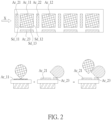
- FIG.2 is a top view diagram and a side view diagram of the antenna module 100 illustrated in FIG.1 .
- the upper diagram of FIG.2 is a top view of the antenna module 100 illustrated in FIG.1
- the lower diagram of FIG.2 is a side view viewed from the X direction of the upper diagram in FIG.2 .
- the antenna module 100 comprises a substrate Sb, at least one first antenna array (two first antenna arrays Ar_11, Ar_12 are used as examples for explaining), and at least one second antenna array (three second antenna arrays Ar_21, Ar_22, Ar_23 are used as examples for explaining).
- the substrate Sb is a PCB (Printed Circuit Board), but it can be any other type of substrate.
- Each of the first antenna arrays Ar_11, Ar_12 is located on the substrate Sb, comprises at least one first antenna, and has a first maximum radiation direction.
- Each of the second antenna arrays Ar_21, Ar_22, Ar_23 is located on the substrate Sb, comprises at least one second antenna, and has a second maximum radiation direction.
- the second antenna array may be parallel with a side of the first antenna array.
- the second antenna arrays Ar_21, Ar_22 are respectively parallel with sides Sd_11, Sd_12 of the first antenna array Ar_11.
- the antenna module 100 comprises a plurality of the first antenna arrays, and the second antenna array is located between the first antenna arrays.
- the second antenna array Ar_22 is provided between the first antenna arrays Ar_11, Ar_12.
- the antenna module 100 comprises a plurality of second antenna arrays, wherein one of the second antenna array is parallel with a first side of the first antenna array and another of the second antenna array is parallel with a second side of the first antenna array, wherein the first side and the second side are perpendicular with each other.
- the second antenna array is parallel with the side Sd_11 (the first side)
- the second antenna array Ar_23 is parallel with the side Sd_13 (the second side) which is perpendicular with the side Sd_11.
- the first antenna array may be located between the second antenna arrays.
- the first antenna array Ar_11 is located between the second antenna arrays Ar_21, Ar_22.
- the first arrays Ar_11, Ar_12 have a first maximum radiation direction and the second antenna arrays Ar_21, Ar_22, Ar_23 have a second maximum radiation direction.
- the first arrays Ar_11, Ar_12 are broad side antenna arrays and the second antenna arrays Ar_21, Ar_22 are end-fire antenna arrays.
- the first maximum radiation direction is perpendicular with the substrate Sb and the second maximum radiation direction is parallel with the substrate Sb. Since the antenna module 100 comprises first arrays Ar_11, Ar_12 and the second antenna arrays Ar_21, Ar_22, Ar_23 which are provided on the substrate Sb, the antenna module 100 can have two maximum radiation directions rather than only one maximum radiation direction.
- the first maximum radiation direction and the second maximum radiation direction can be any two different directions.
- the first maximum radiation direction and the second maximum radiation direction can be changed via changing designs of the first antenna and the second antenna, or via changing tilting angles of the first antenna array Ar_11, Ar_12 and the second antenna array Ar_21, Ar_22, Ar_23.
- the antenna module 100 may be further connected to other components.
- the antenna module 100 is coupled to a communication circuit 101 (e.g., an RFIC) and a connector 103.
- the communication circuit 101 which is molding in the embodiment of FIG.1 , may be configured to transmit/receive signals, or configured to up-convert or to down-convert a signal frequency.
- the communication circuit 101 is molding by protection material.
- the connector 103 may be configured to receive power or control signals for the first antenna arrays Ar_11, Ar_12, the second antenna arrays Ar_21, Ar_22, Ar_23 or the communication circuit 101.
- the first antenna array has a combined polarization which has two directions of polarization in a single one of the first antenna array, and the second antenna array has two directions of polarization in two separate ones of the second antenna arrays.
- the first antenna array Ar_11 provides vertical polarization and horizontal polarization.
- the second antenna array Ar_21 provides only the vertical polarization and the second antenna array Ar_23 provides only the horizontal polarization.
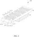
- FIG.3 and FIG.4 are stereograms illustrating antenna modules according to different embodiments of the present application.
- some second antenna arrays are changed from rectangles to ovals.
- the second antenna array Ar_23 is changed from a rectangle to an oval.
- the antenna module further comprises a second antenna array AR_24.
- the second antenna array AR_24 is parallel with a side Sd_14 of the first antenna array AR_11
- the second antenna array AR_23 is parallel with a side Sd_13 of the first antenna array AR_11.
- the sides Sd_13, Sd_14 are parallel with each other.
- FIG.5 illustrates a stereogram and a side view of an antenna module according to another embodiment of the present application.
- some of the second antenna are ovals shown in FIG.3 , but can be replaced by other shapes, such as the rectangles shown in FIG.1 .
- the upper diagram of FIG.5 is a stereogram illustrating an antenna module according to one embodiment of the present application.
- a the lower diagram of FIG.5 is a side view viewed from the Y direction of the upper diagram in FIG.5 .
- the substrate Sb comprises a first layer SbL_1 and a second layer SbL_2 below the first layer SbL_1.
- the first antenna arrays Ar_11, Ar_12 are located on the first layer SbL_1 and the second antenna arrays Ar_21, Ar_22, Ar_23 are located on the second layer SbL_2.
- a projection image of the second antenna array may be parallel with a side of the first antenna array.
- a projection image of the second antenna array Ar_21 which is projected to the first layer SbL_1, is parallel with a side Sd_11 of the first antenna array Ar_11.
- a projection image of the second antenna array may be located between the first antenna arrays.
- a projection image of the second antenna array Ar_22 which is projected to the first layer SbL_1, is located between the first antenna arrays Ar_11, Ar_12.
- a projection image of the first antenna array may be located between the second antenna arrays.
- a projection image of the first antenna array Ar_11 which is projected to the second layer SbL_2, is located between the second antenna arrays Ar_21, Ar_22.
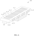
- FIG.6 and FIG.7 are stereograms illustrating antenna modules according to different embodiments of the present application.
- the substrate Sb comprises a first surface Sr_1 and a second surface Sr_21.
- a maximum length of the first surface Sr_1 is identical with a maximum length of the second surface Sr_21. Normal vectors of the first surface Sr_1 and the second surface Sr_21 may be different.
- the first antenna array may be located on the first surface Sr_1, and the second antenna array are located on at least one of the first surface Sr_1 and the second surface Sr_21.
- the first antenna arrays Ar_11, Ar_12 and the second antenna arrays Ar_21, Ar_22, Ar_23 are located on the first surface Sr_1, and the second antenna array Ar_25 is located on the second surface Sr_21.
- the substrate Sb further comprises another second surface Sr_22. At least one second antenna array can be provided on the second surface Sr_22.
- a maximum length of the first surface Sr_1 is longer than a maximum length of the second surface Sr_22. Normal vectors of the first surface Sr_1 and the second surface Sr_22 may be different.
- the first antenna arrays form a single line.
- the first antenna arrays may form at least two lines.
- the first antenna arrays Ar_11, Ar_12 on the first surface Sr_1 form one line and the first antenna arrays Ar_13, Ar_14 on the first surface Sr_1 form another line.
- the second antenna arrays on the first surface Sr_1 form at least two lines and at least one of the second antenna array is located between two of the first antenna arrays.
- the second antenna arrays Ar_21, Ar_22 on the first surface Sr_1 form one line and the second antenna arrays Ar_26, Ar_27 on the first surface Sr_1 form another line.
- the second antenna array Ar_22 is located between the first antenna arrays Ar_11, Ar_12, and the second antenna array Ar_27 is located between the first antenna arrays Ar_13, Ar_14. It will be appreciated that the concepts disclosed in FIG.7 can be applied to the embodiment of FIG.1 .
- FIG.8 is a schematic diagram illustrating auxiliary structures for the antenna module 100, according to embodiments of the present application. Please note, the lower diagram of FIG.2 is used as an example for explaining the embodiment of FIG. 8 . However, the auxiliary structures can be applied in other embodiments disclosed in the present application.
- the antenna module 100 further comprises a metamaterial surface 801 covering the first antenna array and the second antenna array.
- the metamaterial surface 801 can enhance gains of the first antenna array and the second antenna array.
- the antenna module 100 further comprises at least one lens (three lenses LS_1, LS_2, LS_3 in this example) covering the first antenna array and the second antenna array.
- the lenses LS_1, LS_2, LS_3 can enhance gains of the first antenna array and the second antenna array as well.
- the antenna module 100 further comprises a molding layer, which covers at least one of the first antenna array and the second antenna array, or covers all of a surface of the substrate Sb.
- the molding layer can tune the impedance or enhances gains of the first antenna arrays and the second antenna arrays.
- FIG.9 is a schematic illustrating a molding layer is provided for the antenna module, according to one embodiment of the present application.
- the upper diagram of FIG.9 illustrates top view of two examples of the molding layer.
- the lower diagram of FIG.9 is a side view viewed from the Z direction of the upper diagram of FIG.9 .
- the molding layer 901 covers all of a surface of the substrateSb, thus also covers all first antenna arrays and second antenna arrays. Oppositely, in the example 2 of FIG.9 , the molding layer 901 only covers the first antenna arrays. Alternatively preferably, the molding layer 901 only covers at least one second antenna array, or only covers at least one first antenna array and at least one second antenna array.
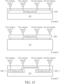
- FIG.10 is a schematic illustrating a switching network is provided to combine radiation of the first antenna array and the second antenna array, according to one embodiment of the present application.
- a switching network 1001 is provided to select horizontal polarization or vertical polarization of the first antenna array, and to select horizontal polarization or vertical polarization of the second antenna array.
- the vertical polarization of the first antenna array is selected, and the horizontal polarization of the second antenna array is selected.
- the horizontal polarization of the first antenna array is selected, and the vertical polarization of the second antenna array is selected.
- the antenna module 100 can have different radiation combination state.
- the switching network 1001 is integrated to the communication circuit 101.
- the switching network 1001 can also be independent from the communication circuit 101, as shown in the example 2 of FIG.10 .
- the number of the switching network 1001 is not limited to 1.
- two switching networks 1001_1 and 1001_2 are provided.
- FIG.11 is a schematic diagram illustrating a communication device 1100, according to one embodiment of the present application.
- the antenna module provided by the present application can be located at any location of the communication device 1100 rather than limited to an edge of the communication device 1100, since antenna arrays thereof are provided on a single substrate.
- the antenna module 100 can be provided to the top of the communication device 1100 (the location L1), or be provided to the back of the communication device 1100 (the location L2) .
- the antenna module 100 may be connected to a communication circuit 101, which is configured to receive signals or to transmit signals by the antenna module 100.
- the communication device 1100 can further comprise a power supplying device 1101, which is coupled to the antenna module 100 via the connector 103 shown in FIG.1 , to provide power to the antenna module 100.
- the communication device 1100 can comprise any required components, such as the processing circuit 1103 and the memory 1105. Details of the required components are omitted for brevity here.
- the antenna module provided by the present application can have multi maximum radiation directions via antenna modules provided on a single substrate. Accordingly, the size and the cost the antenna module can be reduced, and signal loss caused by traces can be decreased.
Landscapes
- Variable-Direction Aerials And Aerial Arrays (AREA)
Abstract
Description
- This application claims the benefit of
U.S. Provisional Application No. 63/318,800, filed on March 11th, 2022 - For a conventional antenna module, the maximum radiation directions of the antenna arrays are always limited, thus the overall performance of the antenna module is limited since signals come from different directions. Further, the traces between different groups of antennas of the conventional antenna module are complex, thus may cause signal loss and a high cost. Therefore, an antenna module which has more than one maximum radiation directions via simplified structures is needed.
- One objective of the present application is to provide an antenna module which can provide multi maximum radiation directions and has a lower signal loss and a lower cost.
- Another objective of the present application is to provide a communication device which has an antenna module which can provide multi maximum radiation directions and has a lower signal loss and a lower cost. An antenna module and a communication device according to the invention are defined in
claims 1 and 15, respectively. Thedependent claims 2 to 14 define preferred embodiments thereof. - One embodiment of the present application discloses an antenna module, comprising: a substrate; at least one first antenna array, located on the substrate, comprising at least one first antenna and having a first maximum radiation direction; and at least one second antenna array, located on the substrate, comprising at least one second antenna and having a second maximum radiation direction.
- Another embodiment of the present application discloses a communication device, comprising: an antenna module, comprising a connector; a communication circuit, coupled to the antenna module, configured to receive signals or to transmit signals by the antenna module; and a power supplying device, coupled to the antenna module via the connector, configured to provide power to the antenna module. The antenna module comprises: a substrate; at least one first antenna array, located on the substrate, comprising at least one first antenna and having a first maximum radiation direction; and at least one second antenna array, located on the substrate, comprising at least one second antenna and having a second maximum radiation direction.
- In view of above-mentioned embodiments, the antenna module provided by the present application can have multi maximum radiation directions via antenna modules provided on a single substrate. Accordingly, the size and the cost the antenna module can be reduced, and signal loss caused by traces can be decreased.
- These and other objectives of the present invention will no doubt become obvious to those of ordinary skill in the art after reading the following detailed description of the preferred embodiment that is illustrated in the various figures and drawings.
-
-
FIG.1 is a stereogram illustrating an antenna module according to one embodiment of the present application. -
FIG.2 is a top view diagram and a side view diagram of the antenna module illustrated inFIG.1 . -
FIG.3 andFIG.4 are stereograms illustrating antenna modules according to different embodiments of the present application. -
FIG.5 illustrates a stereogram and a side view of an antenna module according to another embodiment of the present application. -
FIG.6 andFIG.7 are stereograms illustrating antenna modules according to different embodiments of the present application. -
FIG.8 is a schematic diagram illustrating auxiliary structures for the antenna module, according to embodiments of the present application. -
FIG.9 is a schematic illustrating a molding layer is provided for the antenna module, according to one embodiment of the present application. -
FIG.10 is a schematic illustrating a switching network is provided to combine radiation of the first antenna array and the second antenna array, according to one embodiment of the present application. -
FIG.11 is a schematic diagram illustrating a communication device, according to one embodiment of the present application. - Several embodiments are provided in following descriptions to explain the concept of the present invention. The term "first", "second", "third" in following descriptions are only for the purpose of distinguishing different one elements, and do not mean the sequence of the elements. For example, a first device and a second device only mean these devices can have the same structure but are different devices.
-
FIG.1 is a stereogram illustrating anantenna module 100 according to one embodiment of the present application.FIG.2 is a top view diagram and a side view diagram of theantenna module 100 illustrated inFIG.1 . Specifically, the upper diagram ofFIG.2 is a top view of theantenna module 100 illustrated inFIG.1 , and the lower diagram ofFIG.2 is a side view viewed from the X direction of the upper diagram inFIG.2 . Please also refer toFIG.2 while referring toFIG.1 , to understand the concepts of the present application for more clarity. - As shown in
FIG.1 , theantenna module 100 comprises a substrate Sb, at least one first antenna array (two first antenna arrays Ar_11, Ar_12 are used as examples for explaining), and at least one second antenna array (three second antenna arrays Ar_21, Ar_22, Ar_23 are used as examples for explaining). Preferably, the substrate Sb is a PCB (Printed Circuit Board), but it can be any other type of substrate. Each of the first antenna arrays Ar_11, Ar_12 is located on the substrate Sb, comprises at least one first antenna, and has a first maximum radiation direction. Each of the second antenna arrays Ar_21, Ar_22, Ar_23 is located on the substrate Sb, comprises at least one second antenna, and has a second maximum radiation direction. - The second antenna array may be parallel with a side of the first antenna array. For example, as shown in the upper diagram of
FIG.2 , the second antenna arrays Ar_21, Ar_22 are respectively parallel with sides Sd_11, Sd_12 of the first antenna array Ar_11.Preferably, theantenna module 100 comprises a plurality of the first antenna arrays, and the second antenna array is located between the first antenna arrays. For example, as shown in the upper diagram ofFIG.2 , the second antenna array Ar_22 is provided between the first antenna arrays Ar_11, Ar_12. - Preferably, the
antenna module 100 comprises a plurality of second antenna arrays, wherein one of the second antenna array is parallel with a first side of the first antenna array and another of the second antenna array is parallel with a second side of the first antenna array, wherein the first side and the second side are perpendicular with each other. For example, the second antenna array is parallel with the side Sd_11 (the first side), and the second antenna array Ar_23 is parallel with the side Sd_13 (the second side) which is perpendicular with the side Sd_11. Additionally, the first antenna array may be located between the second antenna arrays. For example, the first antenna array Ar_11 is located between the second antenna arrays Ar_21, Ar_22. - As above-mentioned, the first arrays Ar_11, Ar_12 have a first maximum radiation direction and the second antenna arrays Ar_21, Ar_22, Ar_23 have a second maximum radiation direction. Preferably, the first arrays Ar_11, Ar_12 are broad side antenna arrays and the second antenna arrays Ar_21, Ar_22 are end-fire antenna arrays. Accordingly, as shown in the lower diagram of
FIG.2 , the first maximum radiation direction is perpendicular with the substrate Sb and the second maximum radiation direction is parallel with the substrate Sb. Since theantenna module 100 comprises first arrays Ar_11, Ar_12 and the second antenna arrays Ar_21, Ar_22, Ar_23 which are provided on the substrate Sb, theantenna module 100 can have two maximum radiation directions rather than only one maximum radiation direction. - However, the first maximum radiation direction and the second maximum radiation direction can be any two different directions. Preferably, the first maximum radiation direction and the second maximum radiation direction can be changed via changing designs of the first antenna and the second antenna, or via changing tilting angles of the first antenna array Ar_11, Ar_12 and the second antenna array Ar_21, Ar_22, Ar_23.
- The
antenna module 100 may be further connected to other components. For example, in the embodiment ofFIG.1 , theantenna module 100 is coupled to a communication circuit 101 (e.g., an RFIC) and aconnector 103. Thecommunication circuit 101, which is molding in the embodiment ofFIG.1 , may be configured to transmit/receive signals, or configured to up-convert or to down-convert a signal frequency. In the embodiment ofFIG.1 , thecommunication circuit 101 is molding by protection material. Theconnector 103 may be configured to receive power or control signals for the first antenna arrays Ar_11, Ar_12, the second antenna arrays Ar_21, Ar_22, Ar_23 or thecommunication circuit 101. - Preferably, the first antenna array has a combined polarization which has two directions of polarization in a single one of the first antenna array, and the second antenna array has two directions of polarization in two separate ones of the second antenna arrays. For example, in the embodiment of
FIG.1 , the first antenna array Ar_11 provides vertical polarization and horizontal polarization. Also, in the embodiment ofFIG.1 , the second antenna array Ar_21 provides only the vertical polarization and the second antenna array Ar_23 provides only the horizontal polarization. - The arrangement, size, and locations of the first antenna arrays and the second antenna arrays are not limited to the embodiments illustrated in
FIG.1 andFIG.2 .FIG.3 andFIG.4 are stereograms illustrating antenna modules according to different embodiments of the present application. In the embodiment ofFIG.3 , some second antenna arrays are changed from rectangles to ovals. For example, the second antenna array Ar_23 is changed from a rectangle to an oval. In the embodiment ofFIG.4 , the antenna module further comprises a second antenna array AR_24. In such case, the second antenna array AR_24 is parallel with a side Sd_14 of the first antenna array AR_11, and the second antenna array AR_23 is parallel with a side Sd_13 of the first antenna array AR_11. The sides Sd_13, Sd_14 are parallel with each other. -
FIG.5 illustrates a stereogram and a side view of an antenna module according to another embodiment of the present application. Please note, in the embodiment ofFIG.5 , some of the second antenna are ovals shown inFIG.3 , but can be replaced by other shapes, such as the rectangles shown inFIG.1 . The upper diagram ofFIG.5 is a stereogram illustrating an antenna module according to one embodiment of the present application. Also, a the lower diagram ofFIG.5 is a side view viewed from the Y direction of the upper diagram inFIG.5 . In the embodiment ofFIG.5 , the substrate Sb comprises a first layer SbL_1 and a second layer SbL_2 below the first layer SbL_1. The first antenna arrays Ar_11, Ar_12 are located on the first layer SbL_1 and the second antenna arrays Ar_21, Ar_22, Ar_23 are located on the second layer SbL_2. - In such case, a projection image of the second antenna array may be parallel with a side of the first antenna array. For example, a projection image of the second antenna array Ar_21, which is projected to the first layer SbL_1, is parallel with a side Sd_11 of the first antenna array Ar_11. Further, a projection image of the second antenna array may be located between the first antenna arrays. For example, a projection image of the second antenna array Ar_22, which is projected to the first layer SbL_1, is located between the first antenna arrays Ar_11, Ar_12. Additionally, a projection image of the first antenna array may be located between the second antenna arrays. For example, a projection image of the first antenna array Ar_11, which is projected to the second layer SbL_2, is located between the second antenna arrays Ar_21, Ar_22.
-
FIG.6 andFIG.7 are stereograms illustrating antenna modules according to different embodiments of the present application. In the embodiment ofFIG.6 , the substrate Sb comprises a first surface Sr_1 and a second surface Sr_21. A maximum length of the first surface Sr_1 is identical with a maximum length of the second surface Sr_21. Normal vectors of the first surface Sr_1 and the second surface Sr_21 may be different. In such case, the first antenna array may be located on the first surface Sr_1, and the second antenna array are located on at least one of the first surface Sr_1 and the second surface Sr_21. For example, the first antenna arrays Ar_11, Ar_12 and the second antenna arrays Ar_21, Ar_22, Ar_23 are located on the first surface Sr_1, and the second antenna array Ar_25 is located on the second surface Sr_21. Preferably, the substrate Sb further comprises another second surface Sr_22. At least one second antenna array can be provided on the second surface Sr_22. A maximum length of the first surface Sr_1 is longer than a maximum length of the second surface Sr_22. Normal vectors of the first surface Sr_1 and the second surface Sr_22 may be different. - In above-mentioned embodiments, the first antenna arrays form a single line. However, Preferably, the first antenna arrays may form at least two lines. For example, as shown in
FIG.7 , the first antenna arrays Ar_11, Ar_12 on the first surface Sr_1 form one line and the first antenna arrays Ar_13, Ar_14 on the first surface Sr_1 form another line. In such case, the second antenna arrays on the first surface Sr_1 form at least two lines and at least one of the second antenna array is located between two of the first antenna arrays. For example, the second antenna arrays Ar_21, Ar_22 on the first surface Sr_1 form one line and the second antenna arrays Ar_26, Ar_27 on the first surface Sr_1 form another line. Also, the second antenna array Ar_22 is located between the first antenna arrays Ar_11, Ar_12, and the second antenna array Ar_27 is located between the first antenna arrays Ar_13, Ar_14. It will be appreciated that the concepts disclosed inFIG.7 can be applied to the embodiment ofFIG.1 . - Some auxiliary structures can be provided for improving the performance of the
antenna module 100.FIG.8 is a schematic diagram illustrating auxiliary structures for theantenna module 100, according to embodiments of the present application. Please note, the lower diagram ofFIG.2 is used as an example for explaining the embodiment ofFIG. 8 . However, the auxiliary structures can be applied in other embodiments disclosed in the present application. - In the upper diagram of
FIG.8 , theantenna module 100 further comprises ametamaterial surface 801 covering the first antenna array and the second antenna array. Themetamaterial surface 801 can enhance gains of the first antenna array and the second antenna array. In the lower diagram ofFIG.8 , theantenna module 100 further comprises at least one lens (three lenses LS_1, LS_2, LS_3 in this example) covering the first antenna array and the second antenna array. The lenses LS_1, LS_2, LS_3 can enhance gains of the first antenna array and the second antenna array as well. - Preferably, the
antenna module 100 further comprises a molding layer, which covers at least one of the first antenna array and the second antenna array, or covers all of a surface of the substrate Sb. The molding layer can tune the impedance or enhances gains of the first antenna arrays and the second antenna arrays.FIG.9 is a schematic illustrating a molding layer is provided for the antenna module, according to one embodiment of the present application. The upper diagram ofFIG.9 illustrates top view of two examples of the molding layer. Also, the lower diagram ofFIG.9 is a side view viewed from the Z direction of the upper diagram ofFIG.9 . - In the example 1 of
FIG.9 , themolding layer 901 covers all of a surface of the substrateSb, thus also covers all first antenna arrays and second antenna arrays. Oppositely, in the example 2 ofFIG.9 , themolding layer 901 only covers the first antenna arrays. Alternatively preferably, themolding layer 901 only covers at least one second antenna array, or only covers at least one first antenna array and at least one second antenna array. - Preferably, the radiations of the first antenna array and the second antenna array can be selected and combined via a switching network.
FIG.10 is a schematic illustrating a switching network is provided to combine radiation of the first antenna array and the second antenna array, according to one embodiment of the present application. As shown in the example 1 ofFIG.10 , aswitching network 1001 is provided to select horizontal polarization or vertical polarization of the first antenna array, and to select horizontal polarization or vertical polarization of the second antenna array. For example, the vertical polarization of the first antenna array is selected, and the horizontal polarization of the second antenna array is selected. For another example, the horizontal polarization of the first antenna array is selected, and the vertical polarization of the second antenna array is selected. By this way, theantenna module 100 can have different radiation combination state. - In the example 1 of
FIG.10 , theswitching network 1001 is integrated to thecommunication circuit 101. However, theswitching network 1001 can also be independent from thecommunication circuit 101, as shown in the example 2 ofFIG.10 . Further, the number of theswitching network 1001 is not limited to 1. As shown in example 3 ofFIG.10 , two switching networks 1001_1 and 1001_2 are provided. - The antenna modules illustrated in above-mentioned embodiments can be applied to a communication device such as a mobile phone or a tablet computer.
FIG.11 is a schematic diagram illustrating acommunication device 1100, according to one embodiment of the present application. The antenna module provided by the present application can be located at any location of thecommunication device 1100 rather than limited to an edge of thecommunication device 1100, since antenna arrays thereof are provided on a single substrate. For example, as shown inFIG.11 , theantenna module 100 can be provided to the top of the communication device 1100 (the location L1), or be provided to the back of the communication device 1100 (the location L2) . As above-mentioned, theantenna module 100 may be connected to acommunication circuit 101, which is configured to receive signals or to transmit signals by theantenna module 100. Thecommunication device 1100 can further comprise apower supplying device 1101, which is coupled to theantenna module 100 via theconnector 103 shown inFIG.1 , to provide power to theantenna module 100. Thecommunication device 1100 can comprise any required components, such as theprocessing circuit 1103 and thememory 1105. Details of the required components are omitted for brevity here. - In view of above-mentioned embodiments, the antenna module provided by the present application can have multi maximum radiation directions via antenna modules provided on a single substrate. Accordingly, the size and the cost the antenna module can be reduced, and signal loss caused by traces can be decreased.
- Those skilled in the art will readily observe that numerous modifications and alterations of the device and method may be made while retaining the teachings of the invention. Accordingly, the above disclosure should be construed as limited only by the metes and bounds of the appended claims.
Claims (15)
- An antenna module (100), comprising:a substrate (Sb);at least one first antenna array (Ar_11, Ar_12), located on the substrate (Sb), comprising at least one first antenna and having a first maximum radiation direction; andat least one second antenna array (Ar_21, Ar_22, Ar_23), located on the substrate (Sb), comprising at least one second antenna and having a second maximum radiation direction.
- The antenna module (100) of claim 1, wherein the first antenna array (Ar_11, Ar_12) is a broad side antenna array and the second antenna array (Ar_21, Ar_22, Ar_23) is an end-fire antenna array.
- The antenna module (100) of claim 1 or 2, wherein the second antenna array (Ar_21, Ar_22, Ar_23) is parallel with a side of the first antenna array (Ar_11, Ar_12), or a projection image of the second antenna array (Ar_21, Ar_22, Ar_23) is parallel with a side of the first antenna array (Ar_11, Ar_12).
- The antenna module (100) of any one of claims 1 to 3, comprising a plurality of the first antenna arrays (Ar_11, Ar_12), wherein the second antenna array (Ar_21, Ar_22, Ar_23) is located between the first antenna arrays (Ar_11, Ar_12), or a projection image of the second antenna array (Ar_21, Ar_22, Ar_23) is located between the first antenna arrays (Ar_11, Ar_12); and/or
comprising a plurality of the second antenna arrays (Ar_21, Ar_22, Ar_23), wherein the first antenna array (Ar_11, Ar_12) is located between the second antenna arrays (Ar_21, Ar_22, Ar_23) or a projection image of the first antenna array (Ar_11, Ar_12) is located between the second antenna arrays (Ar_21, Ar_22, Ar_23) . - The antenna module (100) of any one of claims 1 to 4, wherein the substrate (Sb) comprises a first surface (Sr_1) and a second surface (Sr_21), wherein the first antenna array (Ar_11, Ar_12) is located on the first surface (Sr_1), and the second antenna array (Ar_21, Ar_22, Ar_23) is located on at least one of the first surface (Sr_1) and the second surface (Sr_21).
- The antenna module (100) of claim 5, wherein a maximum length of the first surface (Sr_1) is identical with a maximum length of the second surface (Sr_21); or
wherein a maximum length of the first surface (Sr_1) is longer than a maximum length of the second surface (Sr_21). - The antenna module (100) of claim 5 or 6, comprising a plurality of the first antenna arrays (Ar_11, Ar_12) and a plurality of the second antenna arrays (Ar_21, Ar_22, Ar_23), wherein the first antenna arrays (Ar_11, Ar_12) on the first surface (Sr_1) form at least two lines, wherein the second antenna arrays (Ar_21, Ar_22, Ar_23) on the first surface (Sr_1) form at least two lines and at least one of the second antenna arrays (Ar_21, Ar_22, Ar_23) is located between two of the first antenna arrays (Ar_11, Ar_12) .
- The antenna module (100) of any one of claims 1 to 7, further comprising a metamaterial surface (801) covering the first antenna array (Ar_11, Ar_12) and the second antenna array (Ar_21, Ar_22, Ar_23).
- The antenna module (100) of any one of claims 1 to 8, further comprising at least one lens (Ls_1, Ls_2, Ls_3) covering the first antenna array (Ar_11, Ar_12) and the second antenna array (Ar_21, Ar_22, Ar_23).
- The antenna module (100) of any one of claims 1 to 9, further comprising a molding layer (901), wherein the molding layer (901) covers at least one of the first antenna array (Ar_11, Ar_12) and the second antenna array (Ar_21, Ar_22, Ar_23), or covers all of a surface of the substrate which the first antenna array (Ar_11, Ar_12) is provided on.
- The antenna module (100) of any one of claims 1 to 10, further comprising a switching network (1001) configured to combine radiation of the first antenna array (Ar_11, Ar_12) and the second antenna array (Ar_21, Ar_22, Ar_23) in different radiation directions.
- The antenna module (100) of claim 11, coupled to a communication circuit (101), wherein the switching network (1001) is integrated to the communication circuit (101) or independent from the communication circuit (101).
- The antenna module (100) of any one of claims 1 to 12, wherein the first antenna array (Ar_11, Ar_12) has a combined polarization which has two directions of polarization in a single one of the first antenna array (Ar_11, Ar_12), and the second antenna array (Ar_21, Ar_22, Ar_23) has two directions of polarization in two separate ones of the second antenna arrays (Ar_21, Ar_22, Ar_23) .
- The antenna module (100) of any one of claims 1 to 13, comprising a plurality of second antenna arrays (Ar_21, Ar_22, Ar_23), wherein one of the second antenna arrays (Ar_21, Ar_22, Ar_23) is parallel with a first side (Sd_11) of the first antenna array (Ar_11, Ar_12) and another of the second antenna arrays (Ar_21, Ar_22, Ar_23) is parallel with a second side (Sd_13) of the first antenna array (Ar_11, Ar_12), wherein the first side (Sd_11) and the second side (Sd_13) are perpendicular with each other.
- A communication device (1100), comprising:an antenna module (100) according to any one of the preceding claims, comprising a connector (103);a communication circuit (101), coupled to the antenna module (100), configured to receive signals or to transmit signals by the antenna module (100); anda power supplying device (1101), coupled to the antenna module (100) via the connector (103), configured to provide power to the antenna module (100).
Applications Claiming Priority (2)
| Application Number | Priority Date | Filing Date | Title |
|---|---|---|---|
| US202263318800P | 2022-03-11 | 2022-03-11 | |
| US18/116,251 US12500355B2 (en) | 2022-03-11 | 2023-03-01 | Antenna module and communication device using the antenna module |
Publications (2)
| Publication Number | Publication Date |
|---|---|
| EP4243210A1 true EP4243210A1 (en) | 2023-09-13 |
| EP4243210B1 EP4243210B1 (en) | 2025-11-26 |
Family
ID=85556699
Family Applications (1)
| Application Number | Title | Priority Date | Filing Date |
|---|---|---|---|
| EP23160715.1A Active EP4243210B1 (en) | 2022-03-11 | 2023-03-08 | Antenna module and communication device using the antenna module |
Country Status (3)
| Country | Link |
|---|---|
| US (1) | US12500355B2 (en) |
| EP (1) | EP4243210B1 (en) |
| TW (1) | TWI901939B (en) |
Citations (6)
| Publication number | Priority date | Publication date | Assignee | Title |
|---|---|---|---|---|
| US20080272955A1 (en) * | 2007-05-04 | 2008-11-06 | Yonak Serdar H | Active radar system |
| US20170222333A1 (en) * | 2014-10-20 | 2017-08-03 | Murata Manufacturing Co., Ltd. | Wireless communication module |
| US20170222325A1 (en) * | 2014-10-20 | 2017-08-03 | Murata Manufacturing Co., Ltd. | Antenna module |
| US20190165454A1 (en) * | 2017-11-27 | 2019-05-30 | Samsung Electronics Co., Ltd. | Arrangement structure for communication device and electronic device including the same |
| US20200243983A1 (en) * | 2017-10-27 | 2020-07-30 | Robert Bosch Gmbh | Radar sensor having a plurality of main beam directions |
| WO2021251515A1 (en) * | 2020-06-10 | 2021-12-16 | 엘지전자 주식회사 | Electronic device having antenna |
Family Cites Families (6)
| Publication number | Priority date | Publication date | Assignee | Title |
|---|---|---|---|---|
| US9905922B2 (en) * | 2011-08-31 | 2018-02-27 | Qualcomm Incorporated | Wireless device with 3-D antenna system |
| US9806422B2 (en) * | 2013-09-11 | 2017-10-31 | International Business Machines Corporation | Antenna-in-package structures with broadside and end-fire radiations |
| US11101562B2 (en) * | 2018-06-13 | 2021-08-24 | Mediatek Inc. | Multi-band dual-polarized antenna structure and wireless communication device using the same |
| WO2020141018A1 (en) * | 2019-01-03 | 2020-07-09 | Huawei Technologies Co., Ltd. | Beam steering antenna structure and electronic device comprising said structure |
| TWI704726B (en) * | 2019-04-10 | 2020-09-11 | 佳邦科技股份有限公司 | Co-construction antenna module |
| US10749248B1 (en) | 2019-09-23 | 2020-08-18 | Qualcomm Incorporated | Antenna module placement and housing for reduced power density exposure |
-
2023
- 2023-03-01 US US18/116,251 patent/US12500355B2/en active Active
- 2023-03-08 EP EP23160715.1A patent/EP4243210B1/en active Active
- 2023-03-10 TW TW112108943A patent/TWI901939B/en active
Patent Citations (6)
| Publication number | Priority date | Publication date | Assignee | Title |
|---|---|---|---|---|
| US20080272955A1 (en) * | 2007-05-04 | 2008-11-06 | Yonak Serdar H | Active radar system |
| US20170222333A1 (en) * | 2014-10-20 | 2017-08-03 | Murata Manufacturing Co., Ltd. | Wireless communication module |
| US20170222325A1 (en) * | 2014-10-20 | 2017-08-03 | Murata Manufacturing Co., Ltd. | Antenna module |
| US20200243983A1 (en) * | 2017-10-27 | 2020-07-30 | Robert Bosch Gmbh | Radar sensor having a plurality of main beam directions |
| US20190165454A1 (en) * | 2017-11-27 | 2019-05-30 | Samsung Electronics Co., Ltd. | Arrangement structure for communication device and electronic device including the same |
| WO2021251515A1 (en) * | 2020-06-10 | 2021-12-16 | 엘지전자 주식회사 | Electronic device having antenna |
Non-Patent Citations (1)
| Title |
|---|
| EVANS R J ET AL: "Consumer radar: Technology and limitations", 2013 INTERNATIONAL CONFERENCE ON RADAR, IEEE, 9 September 2013 (2013-09-09), pages 21 - 26, XP032519500, DOI: 10.1109/RADAR.2013.6651953 * |
Also Published As
| Publication number | Publication date |
|---|---|
| TW202341570A (en) | 2023-10-16 |
| US20230291127A1 (en) | 2023-09-14 |
| US12500355B2 (en) | 2025-12-16 |
| EP4243210B1 (en) | 2025-11-26 |
| TWI901939B (en) | 2025-10-21 |
Similar Documents
| Publication | Publication Date | Title |
|---|---|---|
| US20250046989A1 (en) | Antenna module, communication device mounted with the same, and circuit board | |
| EP3993368B1 (en) | Display module and mobile terminal | |
| CN210270842U (en) | Display panel and terminal equipment | |
| US11217894B2 (en) | Antenna structure | |
| CN112751170A (en) | Electronic device with 5G antenna | |
| US10651557B2 (en) | C-fed antenna formed on multi-layer printed circuit board edge | |
| US12015192B2 (en) | Terminal device | |
| CN113169441A (en) | Beam steering antenna structure and electronic device comprising said structure | |
| DE112021004407T5 (en) | Antenna module and communication device equipped with the same | |
| US11901614B2 (en) | Low loss wideband radiator for base station antenna | |
| US11837790B2 (en) | Circularly polarized array antenna and circularly polarized array antenna module | |
| US20240106106A1 (en) | Antenna module and communication device equipped with the antenna module | |
| US12500355B2 (en) | Antenna module and communication device using the antenna module | |
| US12261368B2 (en) | Antenna device and communication device | |
| CN112768937B (en) | High isolation phased array antenna module and phased array antenna array | |
| US20240079767A1 (en) | Antenna module | |
| CN116742363A (en) | Antenna module and communication equipment using the antenna module | |
| US12261371B2 (en) | Antenna module and communication device incorporating the same | |
| CN112688064B (en) | Antenna devices including antennas and substrates produced using non-transparent materials | |
| US11909119B2 (en) | Circular polarization array antenna device | |
| CN116547868B (en) | Millimeter-wave antenna device and module including such device | |
| US20250087903A1 (en) | Mimo antenna system | |
| US20230121456A1 (en) | Dynamic antenna group and terminal device comprising same | |
| CN214153188U (en) | Multi-port broadband plate-shaped antenna | |
| KR20220078202A (en) | Microstrip antenna and microstrip antenna module including coupling member |
Legal Events
| Date | Code | Title | Description |
|---|---|---|---|
| PUAI | Public reference made under article 153(3) epc to a published international application that has entered the european phase |
Free format text: ORIGINAL CODE: 0009012 |
|
| STAA | Information on the status of an ep patent application or granted ep patent |
Free format text: STATUS: THE APPLICATION HAS BEEN PUBLISHED |
|
| AK | Designated contracting states |
Kind code of ref document: A1 Designated state(s): AL AT BE BG CH CY CZ DE DK EE ES FI FR GB GR HR HU IE IS IT LI LT LU LV MC ME MK MT NL NO PL PT RO RS SE SI SK SM TR |
|
| STAA | Information on the status of an ep patent application or granted ep patent |
Free format text: STATUS: REQUEST FOR EXAMINATION WAS MADE |
|
| 17P | Request for examination filed |
Effective date: 20240220 |
|
| RBV | Designated contracting states (corrected) |
Designated state(s): AL AT BE BG CH CY CZ DE DK EE ES FI FR GB GR HR HU IE IS IT LI LT LU LV MC ME MK MT NL NO PL PT RO RS SE SI SK SM TR |
|
| STAA | Information on the status of an ep patent application or granted ep patent |
Free format text: STATUS: EXAMINATION IS IN PROGRESS |
|
| 17Q | First examination report despatched |
Effective date: 20250422 |
|
| GRAP | Despatch of communication of intention to grant a patent |
Free format text: ORIGINAL CODE: EPIDOSNIGR1 |
|
| STAA | Information on the status of an ep patent application or granted ep patent |
Free format text: STATUS: GRANT OF PATENT IS INTENDED |
|
| RIC1 | Information provided on ipc code assigned before grant |
Ipc: H01Q 21/06 20060101AFI20250825BHEP Ipc: H01Q 21/24 20060101ALI20250825BHEP Ipc: H01Q 19/06 20060101ALN20250825BHEP Ipc: H01Q 1/40 20060101ALN20250825BHEP Ipc: H01Q 1/24 20060101ALN20250825BHEP |
|
| GRAS | Grant fee paid |
Free format text: ORIGINAL CODE: EPIDOSNIGR3 |
|
| GRAA | (expected) grant |
Free format text: ORIGINAL CODE: 0009210 |
|
| STAA | Information on the status of an ep patent application or granted ep patent |
Free format text: STATUS: THE PATENT HAS BEEN GRANTED |
|
| INTG | Intention to grant announced |
Effective date: 20250926 |
|
| AK | Designated contracting states |
Kind code of ref document: B1 Designated state(s): AL AT BE BG CH CY CZ DE DK EE ES FI FR GB GR HR HU IE IS IT LI LT LU LV MC ME MK MT NL NO PL PT RO RS SE SI SK SM TR |
|
| REG | Reference to a national code |
Ref country code: CH Ref legal event code: F10 Free format text: ST27 STATUS EVENT CODE: U-0-0-F10-F00 (AS PROVIDED BY THE NATIONAL OFFICE) Effective date: 20251126 Ref country code: GB Ref legal event code: FG4D |
|
| REG | Reference to a national code |
Ref country code: IE Ref legal event code: FG4D |
|
| REG | Reference to a national code |
Ref country code: DE Ref legal event code: R096 Ref document number: 602023008868 Country of ref document: DE |
|
| PGFP | Annual fee paid to national office [announced via postgrant information from national office to epo] |
Ref country code: FR Payment date: 20251216 Year of fee payment: 4 |
|
| REG | Reference to a national code |
Ref country code: NL Ref legal event code: MP Effective date: 20251126 |
|
| PG25 | Lapsed in a contracting state [announced via postgrant information from national office to epo] |
Ref country code: ES Free format text: LAPSE BECAUSE OF FAILURE TO SUBMIT A TRANSLATION OF THE DESCRIPTION OR TO PAY THE FEE WITHIN THE PRESCRIBED TIME-LIMIT Effective date: 20251126 |
|
| REG | Reference to a national code |
Ref country code: LT Ref legal event code: MG9D |
|
| PG25 | Lapsed in a contracting state [announced via postgrant information from national office to epo] |
Ref country code: NO Free format text: LAPSE BECAUSE OF FAILURE TO SUBMIT A TRANSLATION OF THE DESCRIPTION OR TO PAY THE FEE WITHIN THE PRESCRIBED TIME-LIMIT Effective date: 20260226 |
|
| PGFP | Annual fee paid to national office [announced via postgrant information from national office to epo] |
Ref country code: DE Payment date: 20251110 Year of fee payment: 4 |
|
| PG25 | Lapsed in a contracting state [announced via postgrant information from national office to epo] |
Ref country code: FI Free format text: LAPSE BECAUSE OF FAILURE TO SUBMIT A TRANSLATION OF THE DESCRIPTION OR TO PAY THE FEE WITHIN THE PRESCRIBED TIME-LIMIT Effective date: 20251126 Ref country code: HR Free format text: LAPSE BECAUSE OF FAILURE TO SUBMIT A TRANSLATION OF THE DESCRIPTION OR TO PAY THE FEE WITHIN THE PRESCRIBED TIME-LIMIT Effective date: 20251126 Ref country code: AT Free format text: LAPSE BECAUSE OF FAILURE TO SUBMIT A TRANSLATION OF THE DESCRIPTION OR TO PAY THE FEE WITHIN THE PRESCRIBED TIME-LIMIT Effective date: 20251126 |
|
| PGFP | Annual fee paid to national office [announced via postgrant information from national office to epo] |
Ref country code: AT Payment date: 20260301 Year of fee payment: 4 |
|
| REG | Reference to a national code |
Ref country code: AT Ref legal event code: MK05 Ref document number: 1862071 Country of ref document: AT Kind code of ref document: T Effective date: 20251126 |
|
| PG25 | Lapsed in a contracting state [announced via postgrant information from national office to epo] |
Ref country code: NL Free format text: LAPSE BECAUSE OF FAILURE TO SUBMIT A TRANSLATION OF THE DESCRIPTION OR TO PAY THE FEE WITHIN THE PRESCRIBED TIME-LIMIT Effective date: 20251126 |
|
| PG25 | Lapsed in a contracting state [announced via postgrant information from national office to epo] |
Ref country code: RS Free format text: LAPSE BECAUSE OF FAILURE TO SUBMIT A TRANSLATION OF THE DESCRIPTION OR TO PAY THE FEE WITHIN THE PRESCRIBED TIME-LIMIT Effective date: 20260226 |
|
| PG25 | Lapsed in a contracting state [announced via postgrant information from national office to epo] |
Ref country code: IS Free format text: LAPSE BECAUSE OF FAILURE TO SUBMIT A TRANSLATION OF THE DESCRIPTION OR TO PAY THE FEE WITHIN THE PRESCRIBED TIME-LIMIT Effective date: 20260326 |
|
| PG25 | Lapsed in a contracting state [announced via postgrant information from national office to epo] |
Ref country code: PT Free format text: LAPSE BECAUSE OF FAILURE TO SUBMIT A TRANSLATION OF THE DESCRIPTION OR TO PAY THE FEE WITHIN THE PRESCRIBED TIME-LIMIT Effective date: 20260326 |
|
| PG25 | Lapsed in a contracting state [announced via postgrant information from national office to epo] |
Ref country code: PL Free format text: LAPSE BECAUSE OF FAILURE TO SUBMIT A TRANSLATION OF THE DESCRIPTION OR TO PAY THE FEE WITHIN THE PRESCRIBED TIME-LIMIT Effective date: 20251126 |
|
| PG25 | Lapsed in a contracting state [announced via postgrant information from national office to epo] |
Ref country code: LV Free format text: LAPSE BECAUSE OF FAILURE TO SUBMIT A TRANSLATION OF THE DESCRIPTION OR TO PAY THE FEE WITHIN THE PRESCRIBED TIME-LIMIT Effective date: 20251126 |
|
| PG25 | Lapsed in a contracting state [announced via postgrant information from national office to epo] |
Ref country code: BG Free format text: LAPSE BECAUSE OF FAILURE TO SUBMIT A TRANSLATION OF THE DESCRIPTION OR TO PAY THE FEE WITHIN THE PRESCRIBED TIME-LIMIT Effective date: 20251126 |