EP4243197A2 - A non-reciprocal device comprising asymmetric phase transport of waves - Google Patents
A non-reciprocal device comprising asymmetric phase transport of waves Download PDFInfo
- Publication number
- EP4243197A2 EP4243197A2 EP23181859.2A EP23181859A EP4243197A2 EP 4243197 A2 EP4243197 A2 EP 4243197A2 EP 23181859 A EP23181859 A EP 23181859A EP 4243197 A2 EP4243197 A2 EP 4243197A2
- Authority
- EP
- European Patent Office
- Prior art keywords
- quantum
- waves
- wave
- devices
- black
- Prior art date
- Legal status (The legal status is an assumption and is not a legal conclusion. Google has not performed a legal analysis and makes no representation as to the accuracy of the status listed.)
- Granted
Links
Images





Classifications
-
- H—ELECTRICITY
- H04—ELECTRIC COMMUNICATION TECHNIQUE
- H04B—TRANSMISSION
- H04B10/00—Transmission systems employing electromagnetic waves other than radio-waves, e.g. infrared, visible or ultraviolet light, or employing corpuscular radiation, e.g. quantum communication
- H04B10/70—Photonic quantum communication
-
- H—ELECTRICITY
- H01—ELECTRIC ELEMENTS
- H01P—WAVEGUIDES; RESONATORS, LINES, OR OTHER DEVICES OF THE WAVEGUIDE TYPE
- H01P1/00—Auxiliary devices
- H01P1/32—Non-reciprocal transmission devices
-
- G—PHYSICS
- G01—MEASURING; TESTING
- G01B—MEASURING LENGTH, THICKNESS OR SIMILAR LINEAR DIMENSIONS; MEASURING ANGLES; MEASURING AREAS; MEASURING IRREGULARITIES OF SURFACES OR CONTOURS
- G01B9/00—Measuring instruments characterised by the use of optical techniques
- G01B9/02—Interferometers
-
- G—PHYSICS
- G01—MEASURING; TESTING
- G01B—MEASURING LENGTH, THICKNESS OR SIMILAR LINEAR DIMENSIONS; MEASURING ANGLES; MEASURING AREAS; MEASURING IRREGULARITIES OF SURFACES OR CONTOURS
- G01B2290/00—Aspects of interferometers not specifically covered by any group under G01B9/02
- G01B2290/55—Quantum effects
Definitions
- the present disclosure relates to a quantum device comprising a non-reciprocal transmission structure.
- the disclosed quantum device comprises a transmission asymmetry which is based on asymmetric phase transport of waves.
- the present disclosure also relates to a method for operating such a quantum device and to a use of one or more of such quantum devices in a lot of different devices.
- Non-reciprocal devices i.e., devices that let waves pass differently in one direction than in the other, are widely used in radar technology [1] and optics [3]. They have also been implemented, for example, as devices based on plasmons, magnons, electromagnons, and sound waves (see, e.g., [2-6]).
- Non-reciprocal devices for de Broglie waves can be realized [7] by using Rashba quantum rings [8,9] or asymmetric Aharonov-Bohm rings [10]. Based on interference of the particles' wave functions, these devices let particles pass preferentially in one direction.
- a quantum device comprises a non-reciprocal transmission structure, wherein the transmission structure is designed such that for first waves traversing the transmission structure in a forward direction the phases of the first waves are at least partially conserved, and for second waves traversing the transmission structure in a backward direction, the phases of the second waves are at least partially replaced by random ones, such that the phase conservation is more pronounced in the forward direction than in the backward direction.
- a method for operating a quantum device comprises supplying the first waves to the quantum device, wherein the first waves comprise quanta with energies obtained from a thermal source or with energies E of order kT, such that kT/10 ⁇ E ⁇ 10kT, wherein T is the temperature of the environment.
- one or more quantum devices according to the first aspect are used in one or more of
- Coupled and “connected”, along with derivatives may be used. It should be understood that these terms may be used to indicate that two elements co-operate or interact with each other, regardless whether they are in direct physical or electrical contact, or they are not in direct or physical or electrical contact with each other which means that there can be one or more intermediate elements between the two elements.
- absorber In the following the terms “absorber”, “emitter” or “absorber/emitter” may be used. It should be understood that these terms are to be understood as any kinds of elements which may absorb or emit any kind of waves, particles and quasi-particles and any kind of radiation. The terms particularly refer to black body radiators (see next paragraph), but also to e.g. resistors which may absorb or emit electrons.
- black body and “black body radiators” along with derivatives may be used. It should be understood that the term is used to refer to bodies in a broad sense, to include also solids, liquids, gases, or plasmas that may emit or absorb thermal radiation.
- the body may not be 100% black (such bodies do not exist at all), and may not be designed as a textbook-like black body radiator consisting of a hollow body with a small opening.
- wave is used to describe any wave associated with a quantum object, be it for example the wave of a photon or a de-Broglie wave of a particle or quasi-particle.
- the considered waves are created/modified in elementary interaction processes which must be described quantum mechanically and may undergo quantum mechanical collapse under conditions such as detailed in [20].
- wave also includes wave packets, for examples wave packets with Gaussian envelope functions.
- the non-reciprocal devices described in the present disclosure break the symmetry of the phase conservation of objects depending on the direction with which these pass through the devices.
- the objects may be particles such as electrons or waves such as photons.
- conserveing the average energy and momentum of the object these devices may act in forward direction like transparent or even open windows, but in reverse direction resemble black-body radiators, or more general absorbers/emitters, with incoherent output.
- quantum device When describing and claiming a quantum device in the following, it should be noted that the term "quantum device” is to be understood in a broad and extensive manner. Concerning the function of the devices revealed here, such a device basically acts as a non-reciprocal filter for matter or electromagnetic waves, for example for photons, particle waves, quasiparticle waves of any kind. Concerning its structure it can be understood as an artificial or man-made structure in which, for example, electrical wires or lines are fabricated by different technological methods, including integrated circuit technology. It can, however, also be understood as consisting of or comprising chemical components like, for example, molecules, molecule compounds, molecule rings like benzene rings with side groups, and so on. It furthermore can refer to solid compounds, e.g. with crystalline structures that exert the device function, or to structures fabricated in or from such crystalline structures.
- the devices function due to the fact that the particles like photons or electrons are only excited or are only moving due to their thermal excitation.
- transmission path can be, but does not have to be understood as a material body.
- a material body e.g. a piece of wire or a waveguide, may comprise one transmission path.
- such a material body may comprise two transmission paths, namely two opposing directions of particles propagating through the material body.
- the term is not to be understood as a tangible or material body which is fabricated from a specific material. It is rather to be understood as a virtual path of a particle or wave in space, and may even be placed, e.g. in a gaseous atmosphere.
- one opening such as one slit
- the phase differences associated with the multitude of transmission paths passing through the slit at different positions or angles causes the characteristic single-slit diffraction pattern.
- slit and “double-slit” may refer to a multitude of geometries and systems.
- the openings of the slits may, for example, not be completely open and transparent.
- more than one or two slits may be used, which also may be configured, for example, as arrangements commonly described as zone-plates, metamaterials, or optical crystals.
- atom may refer to single atoms or molecules, but also to a multitude of atoms, molecules or particles with a characteristic behavior characterized by the behavior of single atoms, without or with the presence of superradiance.
- the term also comprises defects in solids, for example color centers, that can absorb and emit waves in a manner as atoms do.
- random is used here to not only describe processes of completely random nature.
- the term is also used to describe, for example, distributions of phases that are so irregular that interference events between waves with such phases are significantly oppressed.
- phase coherent does not necessarily imply that there is no inelastic, phase-breaking scattering taking place in the device. Indeed, as shown in [11], some inelastic scattering, for example with phonons, is compatible with phase coherence of the part of the wave not affected by the scattering and may be beneficial or in some cases even be required for device operation.
- phase coherent should therefore be understood as including either the absence of inelastic, phase-breaking scattering of the transmission of particles in the device, or to also include the presence of such events, provided that a part of the wave with a phase unaffected by phase-breaking scattering events remains.
- any features, remarks, or comments, mentioned in connection with one or more quantum device or a use of one or more quantum devices are to be understood as also disclosing a respective method feature or method step for making the quantum device(s) function or for implementing the quantum device(s) in any kind of greater device or system and driving the quantum device(s) so that such greater device or system will fulfil its desired function.
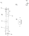
- Fig. 1 comprises Fig. 1A and 1B and shows in Fig. 1A a schematic block representation of a quantum device according to a first embodiment.
- the quantum device 10 of Fig. 1A comprises a non-reciprocal transmission structure which may be connected between a first port 1 and a second port 2.
- the transmission structure is designed such that for first waves traversing the transmission structure in a forward direction from the first port 1 to the second port 2 the phases of the first waves are conserved, and for second waves traversing the transmission structure in a backward direction from the second port 2 to the first port 1, the phases of the second waves are replaced by random ones which are generated by the black bodies 8 having the temperature T.
- the transmission structure comprises a first hybrid coupler 5, a second hybrid coupler 6, and a phase shifter 7, wherein the two hybrid couplers 5 and 6 are interconnected and the phase shifter 7 is connected in-between the two hybrid couplers 5 and 6.
- the quantum device 10 comprises a four-port circulator comprising the first and second ports 1 and 2, a third port 3, and a fourth port 4. At each one of the third and fourth ports 3 and 4 an absorber/emitter 8 and 9 can be disposed.
- Such an absorber/emitter can be comprised of a black body radiator in case of an optical device using electromagnetic waves in, for example, the visible or infrared spectrum, or it can be comprised of a resistor in case of a microwave device using electromagnetic waves in, for example, the microwave region.
- the principle function of the hybrid couplers 5 and 6 is, for example, described on page 322 ff. in [1].
- a signal When a signal enters a hybrid coupler on one of the upper or lower transmission paths, it will receive a phase shift of n/2 when it changes to the respective other transmission path. It will receive no phase shift when it stays horizontally on its transmission path.
- a signal passing through the phase shifter 7 in the direction of the arrow will experience a phase shift of ⁇ and it will experience no phase shift if it passes through the phase shifter 7 in the opposite direction.
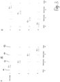
- Fig. 2A shows the quantum device 10 of Fig. 1 in which two transmission paths are marked, which lead from the first port 1 to the second port 2.
- the first one of these transmission paths marked with the letter A experiences a total phase shift of n/2 as there is no phase shift when horizontally passing through the first hybrid coupler 5 and the phase shifter 7, but a phase shift of ⁇ /2 when passing through the second hybrid coupler 6.
- the second one of these transmission paths is marked with the letter B and experiences also a total phase shift of ⁇ /2.
- This phase shift results from the passing through the first hybrid coupler 5 imposing a phase shift of ⁇ /2 onto the signal, wherein there is no phase shift when passing through the second hybrid coupler 6.
- both transmission paths A and B experience a phase shift of ⁇ /2, the respective waves interfere constructively when joining each other in the second hybrid coupler 6 and then leave the second hybrid coupler 6 at port 2.
- Fig. 2B shows the quantum device 10 of Fig. 1 in which two transmission paths are marked which lead from the second port 2 to the first port 1.
- the first one of these transmission paths marked with the letter C experiences a total phase shift of 3 ⁇ ⁇ /2, as there is a first phase shift of ⁇ /2 when passing through the second hybrid coupler 6 and a second phase shift of ⁇ when passing through the phase shifter 7 and no phase shift when horizontally passing through the first hybrid coupler 5.
- the second one of these transmission paths marked with the letter D experiences a total phase shift of n/2, as there is no phase shift when horizontally passing through the second hybrid coupler 6 and a phase shift of ⁇ /2 when passing through the first hybrid coupler 5.
- the two transmission paths C and D will have a phase difference of ⁇ when joining each other in the first hybrid coupler 5, which means that they interfere destructively so that a zero signal will leave the device 10 at the first port 1.
- Fig. 2C shows the quantum device 10 of Fig. 1 in which two transmission paths are marked which lead from the second port 2 to the third port 3.
- the first one of these transmission paths marked with the letter E experiences a total phase shift of 2 ⁇ , as there is a first phase shift of ⁇ /2 when passing through the second hybrid coupler 6, a second phase shift of ⁇ when passing through the phase shifter 7, and a third phase shift of ⁇ /2 when passing through the first hybrid coupler 5.
- the second one of these transmission paths is marked with the letter F. This path experiences a total phase shift of 0 as there is no phase shift when horizontally passing through the second hybrid coupler 6 and as well no phase shift when passing through the first hybrid coupler 5.
- the two transmission paths E and F will have a phase difference of 2 ⁇ when joining each other in the first hybrid coupler 5 which means that they interfere constructively and then leave the device 10 at the third port 3.
- a wave fed into the quantum device 10 at the first port 1 is thus transmitted without distortion to the second port 2 and a wave fed into the quantum device 10 at the second port 2 will be absorbed by the black-body radiator 8 disposed at the third port 3.
- the absorption induces a quantum-mechanical collapse of the wave function [17].
- This collapse causes a loss of information of the wave's phase, because the dissipative coupling of the absorbed wave to the macroscopic bath induces decoherence and thereby parallels the quantum mechanical measurement process [17].
- the black-body radiators 8 and 9 generate a second wave that then passes the quantum device 10 and leaves it at the first port 1, consistent with the second law of thermodynamics.
- the phase of a wave travelling from the first port 1 to the second port 2 is therefore conserved within its unitary evolution, but the phase of a wave leaving the quantum device 10 at the first port 1 is less or not correlated with the phase of a wave entering at the second port 2.
- the energy balance of the transfer process is characterized by non-reciprocal behavior.
- the energy of a wave moving on the transmission path from the first port 1 to the second port 2 is strictly conserved, the energy of waves on the reversed transmission path from the second port 2 to the first port 1 is conserved only on a statistical average.
- the quantum device can have another structure as that shown in Fig. 1 .
- the hybrid couplers 5 und 6 can be either of different nature or may not even exist as will be shown later.
- the ports 3 and 4 do not have to be provided physically.
- the quantum device can be configured such that it functions according to completely different principles as compared to the quantum device of Fig. 1 .
- the quantum device of Fig. 1 is constructed as a static device and as such comprises an intrinsically asymmetric behaviour. It is, however, also possible to construct a quantum device which comprises movable elements so that the asymmetric behaviour is achieved by a specifically controlled movement of these elements. It is furthermore possible to provide a quantum device which does not comprise an intrinsic asymmetry but shows asymmetric behaviour due to the fact that it is embedded in a specific setup or structure. Examples of the above will be shown and explained further below.
- a simple form of a quantum device according to the first aspect may contain a transmission structure which essentially comprises an inelastic scattering center for photons or electrons. It could also be realized by low-loss optical switches in case of photons or a low-loss electronic switches in case of electrons.
- Fig. 3 comprises Fig. 3A and 3B and shows a second embodiment of a quantum device according to the first aspect.
- the quantum device 15 of Fig. 3 comprises a first body 11, a second body 12, a first black body 13, and a second black body 14.
- Figure 3A illustrates the passage of a wave from the first body 11 to the second body 12 at four different time steps 1-4.
- Figure 3B displays the transit of a wave from the second body 12 to the first body 11.
- the first and second bodies 11 and 12 can also be ports like the ports 1 and 2 of the embodiment of Fig. 1 .
- the first and second black bodies 13 and 14 can be moved in and out of the path of the wave. They may for example be formed by appropriately shaped rotating disks.
- a wave may pass unhindered from the first body 11 to the second body 12 as indicated by its constant phase ⁇ 0 remaining unchanged.
- a wave traveling in backward direction, from the second body 12 to the first body 11, however, will be absorbed and statistically reemitted by at least one of the first and second black bodies 13 and 14. Due to the resulting wave function collapse, the information of the initial phase of the wave is lost.
- the wave having phase ⁇ n is absorbed by the second black body 14 which reemits a wave with a random phase ⁇ 1 .
- This wave is then absorbed by the first black body 13 which reemits a wave with a random phase ⁇ 2 .
- this embodiment may act on the complete frequency spectrum of a black-body radiator simultaneously.
- a third embodiment of a quantum device comprises a transmission structure comprising a body that with a probability p causes inelastic scattering and therefore phase information loss of a light wave wherein this embodiment will be described in more detail in connection with the embodiments of Figs. 4 , 5 , 7 , and 8 .
- a method for operating a quantum device comprises supplying the first waves to the quantum device, wherein the first waves comprise quanta with energies obtained from a thermal source or with energies E of order kT, such that kT/10 ⁇ E ⁇ 10kT, wherein T is the temperature of the environment.
- a method for operating a quantum device could alternatively or in addition be defined as comprising providing a source of the first waves, wherein the source of the first waves is held in thermal equilibrium with an environment.
- the environment can be a natural environment like a room being under room temperature, or a place in free nature. It can also be an artificial environment such as the cavity containing the device, or such as a thermal bath provided for example by a water bath or a hot oven.
- a method for operating a quantum device could alternatively or in addition be defined as comprising providing a source of the first waves, wherein the source of the first waves is not actively stimulated, in particular not actively stimulated by non-thermal energy so that it would be possible that the source is actively heated or cooled.
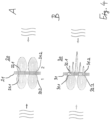
- Fig. 4 comprises Fig. 4A and 4B and relates to the possibility to use the asymmetric phase transmission to create asymmetric interference.
- Fig. 4A is intended only for illustrative purposes and shows an interferometer 20 which comprises an interferometer plate 21 and two slits 21.1 and 21.2 formed in a side-by-side relationship in the plate 21.
- the two slits 21.1 and 21.2 are filled with black-body radiators 22.1 and 22.2, respectively. It is further illustrated in the figure what happens when coherent radiation impinges onto the interferometer 20 from either one of the two sides of the plate 21.
- the two black-body radiators 22.1 and 22.2 will destroy the phases of the incident coherent waves and randomly emit another wave to the other side, the randomly emitted wave carrying a random new phase.
- the black-body radiators 22.1 and 22.2 will emit incoherent radiation to either sides of the plate 21 as it is indicated by the bubble-like radiation cones which typically follows an angular dependence as described by Lambert's radiation law.
- Fig. 4B shows an example of a possible use of the quantum devices according to the first aspect.
- An interferometer 30 comprises an interferometer plate 31 and two slits 31.1 and 31.2 formed in a side-by-side relationship into the interferometer plate 31.
- Quantum devices 32.1 and 32.2 are inserted into the slits 31.1 and 31.2, respectively. It is assumed that the two quantum devices 32.1 and 32.2 both comprise an identical directional orientation and, moreover, a directional orientation such as that of the quantum device 10 as shown in Fig. 1 .
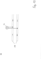
- Fig. 6 comprises Fig. 6A and 6B and shows a conventional commercially available optical 3-ports-circulator in order to illustrate the way in which the quantum devices could be inserted into the slits 31.1 and 31.2.
- the optical circulator comprises the form of a fiber optical device comprising first and third ports 1 and 3 at the left lower end and a second port 2 at the right upper end.
- the sketch in Fig. 6B shows the possible paths of light waves in and out of the device.
- the designation of the ports corresponds to that of the embodiment of Fig. 1 , i.e. light incident on the device from the left side has to be coupled into the device at port 1 and then leaves the device coherently at port 2, whereas light incident on the device from the right side is coupled into the device at port 2 and is then internally guided to port 3. There will be no external fiber connected to port 3. Instead at port 3 a black body radiator is provided at the left-side output of the device.
- a port 4 is provided in the embodiment of Fig. 1 .
- Two such circulators are provided and each one is inserted in one of the two slits of the interferometer.
- the fiber ends at port 2 are favorably have to be oriented in parallel so that they may properly work as a double-slit.
- the quantum devices 32.1 and 32.2 could be realized according to one of the embodiments as shown in Fig. 1 or Fig. 3 .
- the quantum devices 31.1 and 31.2 could also be realized by inelastic scatterers like, e.g. a gas or a lightly opaque solid body or a cluster of scatterers.
- Fig. 4B It is further shown in Fig. 4B what happens when coherent radiation impinges onto the interferometer 30 from either sides of the interferometer plate 31.
- the coherent radiation impinges from the right side onto the interferometer plate 31 i.e. the coherent waves pass through the quantum devices 32.1 and 32.2 in backward direction and thus realize them as pure black-body radiators. Consequently the coherent waves are absorbed in the black body radiators of the quantum devices 32.1 and 32.2 and incoherent radiation with random phases is emitted from either one of the quantum devices 32.1 and 32.2 and emanates from the two slits 31.1 and 31.2 to the left side of the interferometer plate 31 as indicated by the bubble-like radiation cones.
- the coherent waves pass through the quantum devices 32.1 and 32.2 in forward direction so that the phases of the coherent waves are conserved. Consequently, the coherent waves emitted to the right side interfere constructively and lead to a typical double-slit diffraction pattern as shown in the Figure.
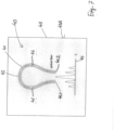
- Fig. 5 comprises Fig. 5A and 5B and shows an extension of the interferometer 30 of Fig. 4B which may lead to a useful device.
- the interferometer 30 is placed in a cavity 33 comprising walls 33A.
- the interferometer 30 is inserted in the cavity 33 in such a way that the interferometer plate 31 extends from one cavity wall to an opposing cavity wall and thus divides the interior of the cavity 33 into two half spaces which are separated from each other by the interferometer plate 31.
- the walls 33A of the left half of the cavity 33 are provided by mirrors, whereas the walls 33A of the right half are black.
- the walls 33A are in thermal equilibrium with an external bath.
- the radiation coming from the left is generated by a particle 34 like e.g. a grain of carbon or a cluster of atoms that acts as a black-body radiator.
- a double-slit diffraction pattern is created in the right half of the cavity 33 (see Fig. 5B ).
- the phase coherence length of thermal radiation in a cavity is not defined in any manner by Planck's spectral radiation density [11].
- the radiation coming from the right is essentially comprised of black-body radiation coming from the walls 33A of the right half and it passes through the quantum devices 32.1 and 32.2 in backward direction leading to incoherent radiation as indicated by the bubble-like cones in the left half (see Fig. 5A ).
- the spatial densities of the radiation in the two halves of the cavity 33 differ.
- the interference characteristic in the right half is inhomogeneous, potentially causing temperature differences of test bodies 35 placed at different locations in the cavity 33, one test body 35 placed at an interference maximum and the other test body 35 placed at an interference minimum of the diffraction pattern.
- This temperature difference sensed by the test bodies 35 may be converted, e.g. by using a thermo-couple device, into useful electric power. It is obvious that the output power can be optimized by varying, for example, the temperature or geometry of the black bodies or of the thermal bath to which the atom may be anchored, or by altering the number of atoms absorbing and reemitting the radiation.
- thermodynamics
- Fig. 7 shows a further example of a possible application of quantum devices according to the first aspect.
- Fig. 7 shows a further embodiment of an optical interferometer.
- the interferometer 40 of Fig. 7 comprises an optical fiber 41 incorporated into a cavity 43, the walls 43A of which are in thermal equilibrium with an external bath.
- a particle like e.g. an atom 42 is embedded, which upon excitation may emit single photons such that each photon coherently propagates in both directions of the fiber.
- the atom 42 is anchored to a thermal bath.
- First and second quantum devices 45 and 46 provided according to the first aspect, are incorporated in the optical fiber 41 in such a way that in both radiation directions of radiation emitted by the atom 42 one quantum device 45 or 46 is arranged wherein the forward directions are directed downwards and the backward directions are directed upwards.
- the two quantum devices 45, 46 can be identical.
- a screen 44 is provided which receives the radiation output by the first and second output ends 41.1 and 41.2 of the optical fiber 41.
- the two waves being emitted by the atom 42 in both directions pass undisturbed through the two quantum devices 45, 46 so that they are still coherent with each other with zero phase difference.
- a double-slit diffraction pattern is created on the screen 44.
- the screen 44 and the diffraction pattern generate coherent light waves being coupled into the optical fiber 41 by means of the two fiber ends 41.1 and 41.2.
- the interference maxima of the diffraction pattern on the screen 44 generate coherent partial waves of zero phase difference in the optical fiber 41
- the interference minima of the diffraction pattern on the screen 44 generate coherent partial waves of a phase difference of ⁇ in the optical fiber 41.
- the two coherent partial waves impinge onto the quantum devices 45, 46 and their wave functions collapse therein.
- waves with random phases are generated by the quantum devices 45, 46 which impinge onto and are absorbed by the atom 42.
- the atom 42 then starts again by generating coherent partial waves being emanated to the right and to the left and having a relative phase difference of zero.
- thermo-couple device may obviously also be used to heat or to cool bodies, using as energy source the thermal energy of the heat bath.
- the quantum devices 45 and 46 could be realized according to one of the embodiments as shown in Fig. 1 or Fig. 3 . As was indicated above, the quantum devices 45 and 46 could also be realized by inelastic scatterers.
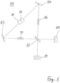
- Fig. 8 shows a further example of a possible application of quantum devices according to the first aspect.
- Fig. 8 shows another form of an interferometer.
- the interferometer 50 of Fig. 8 comprises a mirrored cavity 51 with open ends housing a coherently radiating particle like e.g. an atom 52, first and second highly reflecting mirrors 53 and 54, two quantum devices 55 and 56, a semitransparent mirror 57 and first and second black body radiators 58 and 59.
- the atom 52 is anchored to a thermal bath.
- the two quantum devices 55 and 56 are configured as quantum devices according to the first aspect and can be identical.
- the arrows indicate their respective forward directions in which phase coherence is maintained.
- the mirrored cavity 51 comprises two opposing openings for two light beams respectively passing out of the mirrored cavity 51 in two opposing directions.
- the first and second highly reflecting mirrors 53 and 54 deflect the two light beams onto two light paths, respectively, which two light paths join each other at the semitransparent mirror 57, i.e. an asymmetric beamsplitter, after having passed ideally undisturbed through the quantum devices 55 and 56.
- the setup is configured such that light beams that come from the two quantum devices 55 and 56 without any phase difference are deflected only to the first black body radiator 58.
- the black body radiators 58 and 59 In the opposite direction the black body radiators 58 and 59 generate incoherent black body radiation which impinges onto the semitransparent mirror 57.
- the semitransparent mirror 57 splits up the waves received from the black body radiators 58 and 59 into respective partial waves. These partial waves are pair-wise coherent with each other whereby the partial waves generated out of a wave emitted by black body radiator 58 comprise a phase difference of 0, and the partial waves generated out of a wave emitted by black body radiator 59 comprise a phase difference of ⁇ .
- the quantum devices 55 and 56 destroy the phase coherence of the partial waves and in particular erase the phase difference of ⁇ between the partial waves resulting from the emission of black body radiator 59.
- the quantum devices 55 and 56 effect a collapse of the wave function which means that due to quantum mechanics the arriving wave either passes through the quantum device 55 or through the quantum device 56. As a result, the wave impinges onto the atom 52 either from the right side or from the left side. If the wave is not getting absorbed by the atom 52, it impinges onto the beamsplitter 57 which deflects it to both black body radiators 58 and 59 in equal proportions on a statistical average.
- the first and second black body radiators 58 and 59 initially are at equal temperatures and emit equal amounts of radiative power, but receive radiation of different powers. As a result, a temperature difference is generated between the first and second black body radiators 58 and 59 which can be used, for example, to generate electric power.
- the above-described quantum devices and their applications require some coupling to heat baths which are at a T > 0 K.
- the heat baths may be given by the black bodies 58 and 59 and the black bodies in the quantum devices 55 and 56.
- the medium of such a heat bath can be solid, liquid or gaseous.
- the devices may extract energy from one or of several of the heat baths and transfer the heat energy, e.g. to one or several other heat baths.
- a second device may be thermally connected, such that the black body A2 of the second device becomes cooled to even lower temperatures than the body A1.
- the quantum devices 55 and 56 could be realized according to one of the embodiments as shown in Fig. 1 , Fig. 3 , or Fig. 10 . As was indicated above, the quantum devices 55 and 56 could also be realized by inelastic scatterers that scatter each with a probability p. If set up in the manner described, device operation is achieved, as the phase information of the coherent waves moving from the body 59 to the atom 52 and back to the body 59 - these waves heat body 59 and are therefore detrimental for device operation - is reduced by a factor of (1 - p) ⁇ (1 - p), while the coherent wave generated by the atom 52 and moving to the body 58 is reduced by factor of p only. Also this embodiment may simultaneously act on the complete frequency spectrum of a black-body radiator.
- FIG. 9 shows an example of the use of quantum devices in an electron interferometer.
- An electron interferometer 60 of Fig. 9 comprises an electron source 61, a first quantum device 62 and a second quantum device 63, a first resistor 64 and a second resistor 65, both first and second resistors 64 and 65 connected to ground.
- the interferometer 60 further comprises a first transmission path 66.1 connecting the electron source 61 with a first port of the first quantum device 62, a second transmission path 66.2 connecting the electron source 61 with a first port of the second quantum device 63, a third transmission path 66.3 connecting a second port of the first quantum device 62 with the first resistor 64, a forth transmission path 66.4 connecting a second port of the second quantum device 63 with the first resistor 64, a fifth transmission path 66.5 connecting the second port of the second quantum device 63 with the second resistor 65, and a sixth transmission path 66.6 connecting the second port of the first quantum device 62 with the second resistor 65.
- the first and second resistors 64 and 65 function as electron absorbers and emitters. For effectively absorbing electrons they may have a resistance of 50 Ohm.
- the generating of electrons happens, for example, via the thermal noise, i.e. Johnson/Nyquist noise which is due to the thermal agitation of the charge carriers inside an electrical conductor at equilibrium.
- the interferometer 60 is configured in such a way that electron waves experience a phase shift ⁇ on the third, forth, and fifth transmission paths 66.3, 66.4, and 66.5, and electron waves experience a phase shift of ⁇ + ⁇ on the sixth transmission path 66.6.
- phase shifts can be achieved by designing the transmission paths with the following lengths.
- the electron source 61 corresponds to the atom 42 in the embodiment of Fig. 7 or to the atom 52 in the embodiment of Fig. 8 . It can, for example, as well be an atom which can absorb an electron and emit an electron. It can also be a crystal defect which can as well absorb or emit electrons. In case of the emission of an electron, two partial electron waves are emitted which propagate on the first and second transmission paths 66.1 and 66.2.
- the quantum devices 62 and 63 can be identical and maybe configured as inelastic scattering centers as, for example, crystal defects or phonons coupled into a crystal. They could also be configured, for example, as low-loss electronic switches like, e.g. FETs.
- the transmission paths 66.1 to 66.6 correspond to the beamsplitter 57 in the embodiment of Fig. 8 .
- Fig. 10 shows an implementation of the use of quantum devices according to the present disclosure in a photonic system.
- the photonic system 70 comprises an ensemble of two-level systems TLS 71, two black-body radiators 72 and 73, and a chiral waveguide 74.
- the two level systems 71 are coupled to the chiral waveguide 74 with two different coupling strengths g1 and g2 that depend on the propagation direction of the waves. Comparable couplings are described, for example, in [21].
- the two level systems TLS 71 induced phase-breaking of the photon modes in the waveguide 74 that depends on the direction of travel of the photons.
- This nonreciprocal phase-breaking ultimately induces a non-identical population of the photons in the two black-body cavities 72 and 73.
- a temperature difference will develop between the black-body cavities 72 and 73. Again this temperature difference may be converted, e.g., by using a thermo-couple device, into useful electric power.
- the quantum devices as described in the present disclosure pass information preferably in the forward direction, and hinder the flow of information in the backward direction.
- This valuable functional behavior has obvious applications in data transmission and storage based on conventional or quantum systems. It offers for example the possibility that a user of a quantum system writes data into a quantum memory but is not able to retrieve data stored in this memory, or vice versa.
- the present disclosure also relates to the following further aspects. These aspects refer to devices in which a quantum device according to the first aspect can be implemented so that the respective device fulfills a particular function as will be outlined in the following.
- the present disclosure also relates to a device utilizing coherent emission and at least partial collapses of wave functions to achieve a deviation from one or more of the zeroth law, the second, or the third law of thermodynamics.
- the present disclosure also relates to a device utilizing quantum-mechanical superposition of states and at least partial collapses of wave functions to achieve a deviation from the zeroth, the second, or the third law of thermodynamics.
- the device according to any one of the above further aspects may operate at a temperature in the range of 10 -6 K - 4000 K.
- the device according to any one of the above further aspects may not be coupled to or entangled with a bath in the quantum regime.
- the present disclosure also relates to a device utilizing coherent emission and at least partial quantum-physical collapses of wave functions or quantum-mechanical superposition of states and at least partial collapses of wave functions to generate or to enhance inhomogeneities in the density of the energy distribution of waves or particles in a system.
- the energy distribution may be an energy distribution generated at least partially by thermal energy.
- the present disclosure also relates to a device utilizing coherent emission and at least partial quantum-physical collapses of wave functions or quantum-mechanical superposition of states and at least partial collapses of wave functions to shift a system out of the state of thermal equilibrium.
- the present disclosure also relates to a device utilizing coherent emission and at least partial quantum-physical collapses of wave functions or quantum-mechanical superposition of states and at least partial collapses of wave functions to generate temperature differences within one body or between several bodies.
- phase shifts maybe induced by at least one non-reciprocal component of the device.
- the at least partial quantum physical collapse of the wave function is achieved by the use of a macroscopic body, which may for example be a solid, a liquid, a gas, or a plasma.
- the at least partial quantum physical collapse and an at least partial absorption of the wave function at a body is followed by a statistical reemission of a wave by said body.
- an at least partially quantum physical collapsed wave is statistically replaced by another wave with a random phase.
- the device creates useful work by converting a generated radiation density inhomogeneity or a generated temperature difference into electricity, radiation, optical energy, or other forms of energy, or by using the achieved order in some other manner.
- the device transports mass, particles, energy, heat, momentum, angular momentum, charge, or magnetic moments within one body or between several bodies.
- the device charges a storage system for energy, waves or matter, for example a capacitor or a battery.
- the device heats or cools bodies.
- one or several of the bodies of the device are operated at another base temperature than room temperature, for example by using an additionally provided heating or cooling function.
- an internally or externally created signal is used to control the process.
- the key elements contributing to the apparent violation of the second law are the generation of particle states split into multiple wave packets, the quantum mechanical collapse of the multiple wave-packet states, and the sorting of single and multiple wave-packet states by interference, where the latter step transfers the coherence properties of the wave packets into a useful output signal.
- These robust, single-particle processes are scalable, they function in a wide temperature range including high-temperatures, are compatible with a standard room-type environment, and can be implemented in a large variety of devices acting on many species of quantum waves, including electromagnetic, particle and quasiparticles waves.
Landscapes
- Physics & Mathematics (AREA)
- General Physics & Mathematics (AREA)
- Optics & Photonics (AREA)
- Electromagnetism (AREA)
- Engineering & Computer Science (AREA)
- Computer Networks & Wireless Communication (AREA)
- Signal Processing (AREA)
- Optical Modulation, Optical Deflection, Nonlinear Optics, Optical Demodulation, Optical Logic Elements (AREA)
- Surface Acoustic Wave Elements And Circuit Networks Thereof (AREA)
Abstract
Description
- The present disclosure relates to a quantum device comprising a non-reciprocal transmission structure. The disclosed quantum device comprises a transmission asymmetry which is based on asymmetric phase transport of waves. The present disclosure also relates to a method for operating such a quantum device and to a use of one or more of such quantum devices in a lot of different devices.
- For illustrating background art reference is made to the following prior art:
- 1. D.M. Pozar, Microwave Engineering, J. Wiley and Sons, 4th ed. (2012).
- 2. N. Bahlmann, M. Lohmeyer, M. Wallenhorst, H. Dötsch, and P. Hertel, Optical and Quantum Electronics 30, 323 (1998).
- 3. R.J. Potton, Rep. Prog. Phys. 67, 717 (2004).
- 4. R. Fleury, D.L. Sounas, C.F. Sieck, M.R. Haberman, and A. Alù, Science 343, 518 (2014).
- 5. A.A. Mukhin, A.M. Kuzmenko, V.Yu Ivanov, A.G. Pimenov, A.M. Shuvaev, and V.E. Dziom, Physics-Uspekhi 58, 993 (2015).
- 6. A.C. Mahoney et al., Phys. ).
- 7. J. Mannhart, J. Supercond. Novel. Magn. 31, 1649 (2018). (2018).
- 8. É.I. Rashba, Sov. Phys. Solid State 2, 1109 (1960).
- 9. T. Chakraborty, A. Manaselyan, and M. Barseghyan, "Electronic, Magnetic, and Optical Properties of Quantum Rings in Novel Systems", in V.M. Fomin, "Physics of Quantum Rings" (Springer, 2018).
- 10. Y. Aharonov and D. Bohm, Phys. Rev. B 115, 485 (1959).
- 11. M. Planck, Verhandlungen der Deutschen Physikalischen Gesellschaft 2, 245 (1900).
- 12. C. Elouard, D. Herrera-Martí, B. Huard, and A. Auffèves, Phys. Rev. Lett. 118, 260603 (2017).
- 13. N. Cottet et al., PNAS 114, 7561 (2017).
- 14. J.C. Maxwell, Theory of Heat, Longmans, Green, and Co. (1871).
- 15. Th. M. Nieuwenhuizen, A.E. Allahverdyan, Phys. Rev. E, 036102 (2002).
- 16. Z. Merali, Nature 551, 20, (2017)
- 17. C. Cohen-Tannoudji, B. Diu, F. Laloe, Quantum Mechanics, Wiley, 2005
- 18. L.E. Reichl, "A Modern Course in Statistical Physics", E. Arnold, 1980
- 19. V. Capek and D.P. Sheehan, "Challenges to the Second Law of Thermodynamics", Springer 2005
- 20. Y. Imry, "Introduction to Mesoscopic Physics", Oxford University Press (2002)
- 21. P. Lodahl et al., Nature 541, 473 (2017).
- Non-reciprocal devices, i.e., devices that let waves pass differently in one direction than in the other, are widely used in radar technology [1] and optics [3]. They have also been implemented, for example, as devices based on plasmons, magnons, electromagnons, and sound waves (see, e.g., [2-6]). Non-reciprocal devices for de Broglie waves can be realized [7] by using Rashba quantum rings [8,9] or asymmetric Aharonov-Bohm rings [10]. Based on interference of the particles' wave functions, these devices let particles pass preferentially in one direction.
- In accordance with a first aspect of the present disclosure, a quantum device comprises a non-reciprocal transmission structure, wherein the transmission structure is designed such that for first waves traversing the transmission structure in a forward direction the phases of the first waves are at least partially conserved, and for second waves traversing the transmission structure in a backward direction, the phases of the second waves are at least partially replaced by random ones, such that the phase conservation is more pronounced in the forward direction than in the backward direction.
- In accordance with a second aspect of the present disclosure a method for operating a quantum device according to the first aspect comprises supplying the first waves to the quantum device, wherein the first waves comprise quanta with energies obtained from a thermal source or with energies E of order kT, such that kT/10 < E < 10kT, wherein T is the temperature of the environment.
- In accordance with a third aspect of the present disclosure, one or more quantum devices according to the first aspect are used in one or more of
- a device in which the first waves comprise quanta with energies obtained from a thermal source or with energies E of order kT, such that kT/10 < E < 10kT, wherein T is the temperature of the environment;
- a device utilizing coherent emission and at least partial collapses of wave functions to achieve a deviation from one or more of the zeroth law, the second, or the third law of thermodynamics;
- a device utilizing quantum-mechanical superposition of states and at least partial collapses of wave functions to achieve a deviation from one or more of the zeroth, the second, or the third law of thermodynamics;
- a device utilizing coherent emission and at least partial quantum-physical collapses of wave functions or quantum-mechanical superposition of states and at least partial collapses of wave functions to generate or to enhance inhomogeneities in the density of the energy distribution of waves or particles in a system;
- a device utilizing coherent emission and at least partial quantum-physical collapses of wave functions or quantum-mechanical superposition of states and at least partial collapses of wave functions to shift a system out of the state of thermal equilibrium;
- a device utilizing coherent emission and at least partial quantum-physical collapses of wave functions or quantum-mechanical superposition of states and at least partial collapses of wave functions to generate temperature differences within one body or between several bodies;
- a device comprising an interferometer; and
- a device comprising analog or digital systems for quantum computation, quantum data transmission, or quantum data storage;
- a device comprising an interferometer;
- a device performing quantum computation, quantum data transmission, quantum data storage, heating, cooling, matter transport, energy transport, or power generation.
- The person skilled in the art recognizes additional features and advantages upon reading the following detailed description and upon giving consideration to the accompanying drawings.
- The accompanying drawings are included to provide a further understanding of examples and are incorporated in and constitute a part of this specification. The drawings illustrate examples and together with the description serve to explain principles of examples. Other examples and many of the intended advantages of examples will be readily appreciated as they become better understood by reference to the following detailed description.
-
Fig. 1 comprises Fig. 1A and 1B and shows a schematic block representation (A) and a symbolic representation (B) of a first embodiment of a quantum device according to the first aspect, which embodiment is based on a four-port circulator comprising two hybrid couplers and a phase shifter connected between the hybrid couplers and two black-body radiators disposed at respective two ports. -
Fig. 2 comprisesFig. 2A to 2C and shows the quantum device ofFig. 1 in which first transmission paths extending from a first port to a second port are marked (A), the quantum device ofFig. 1 in which second transmission paths extending from the second port to the first port are marked (B), and the quantum device ofFig. 1 in which third transmission paths extending from the second port to a third port are marked (C). -
Fig. 3 comprisesFig. 3A and 3B and illustrates a second embodiment of a quantum device according to the first aspect.Fig. 3 shows a time sequence of a wave travelling inFig. 3A from a body A to a body B, and inFig. 3B from a body B to a body A, with the value of the wave's phase denoted, wherein two black bodies C and D are inserted in the shown time sequence in the path between bodies A and B. -
Fig. 4 comprisesFig. 4A and 4B and shows for illustrative purposes an example of an optical double-slit interferometer in which the two slits are filled with black-body radiators (A), and an example of a double-slit interferometer in which the two slits are filled with quantum devices according to the first aspect (B). -
Fig. 5 comprisesFig. 5A and 5B and shows the double-slit interferometer ofFig. 5B disposed in a cavity comprising reflecting walls in a situation in which coherent radiation impinges onto the interferometer in a backward direction with respect to the quantum devices (A), and in a forward direction with respect to the quantum devices (B). -
Fig. 6 comprisesFig. 6A and 6B and shows a commercially available 3 ports optical circulator in a perspective representation (A) and in a schematic functional representation (B). -
Fig. 7 shows a schematic representation of an interferometer comprising an optical fiber, two quantum devices according to the first aspect and one coherently radiating atom inserted in the optical fiber, and a screen for receiving an optical diffraction pattern. -
Fig. 8 shows a schematic representation of an interferometer comprising an optical light path comprising a coherently radiating atom, two highly reflecting mirrors collecting the coherent radiation, a semitransparent mirror, and two black body radiators. -
Fig. 9 shows a schematic representation of an example of an electronic interferometer comprising an electron source, two quantum devices, two resistors, and transmission paths connecting the electron source to the quantum devices and the quantum devices to the resistors. -
Fig. 10 comprisesFig. 10(a) and10(b) and illustrates the principle of a further example in which two level systems TLS couple non-symmetrically to the left- and right-moving channels of a chiral waveguide, wherein the TLS interact in a nonlinear manner with the photons travelling in the waveguide and break their phases with different strengths and the coupling between the TLS and the waveguides are therefore specified by two different coupling parameters g1 and g2 (a), and a device implementation of the principle shown in (a), wherein the waveguide is closed into a ring and is coupled to cavities A and B acting as black bodies (b). - In the following description the terms "coupled" and "connected", along with derivatives may be used. It should be understood that these terms may be used to indicate that two elements co-operate or interact with each other, regardless whether they are in direct physical or electrical contact, or they are not in direct or physical or electrical contact with each other which means that there can be one or more intermediate elements between the two elements.
- In the following the terms "absorber", "emitter" or "absorber/emitter" may be used. It should be understood that these terms are to be understood as any kinds of elements which may absorb or emit any kind of waves, particles and quasi-particles and any kind of radiation. The terms particularly refer to black body radiators (see next paragraph), but also to e.g. resistors which may absorb or emit electrons.
- In the following the term "black body" and "black body radiators" along with derivatives may be used. It should be understood that the term is used to refer to bodies in a broad sense, to include also solids, liquids, gases, or plasmas that may emit or absorb thermal radiation. The body may not be 100% black (such bodies do not exist at all), and may not be designed as a textbook-like black body radiator consisting of a hollow body with a small opening.
- The term "wave" is used to describe any wave associated with a quantum object, be it for example the wave of a photon or a de-Broglie wave of a particle or quasi-particle. The considered waves are created/modified in elementary interaction processes which must be described quantum mechanically and may undergo quantum mechanical collapse under conditions such as detailed in [20]. Besides that the term "wave" also includes wave packets, for examples wave packets with Gaussian envelope functions.
- The term "collapse" is used to describe any process causing an at least partially phase-breaking decoherence of quantum-mechanical states.
- The non-reciprocal devices described in the present disclosure break the symmetry of the phase conservation of objects depending on the direction with which these pass through the devices. The objects may be particles such as electrons or waves such as photons. Conserving the average energy and momentum of the object, these devices may act in forward direction like transparent or even open windows, but in reverse direction resemble black-body radiators, or more general absorbers/emitters, with incoherent output.
- When describing and claiming a quantum device in the following, it should be noted that the term "quantum device" is to be understood in a broad and extensive manner. Concerning the function of the devices revealed here, such a device basically acts as a non-reciprocal filter for matter or electromagnetic waves, for example for photons, particle waves, quasiparticle waves of any kind. Concerning its structure it can be understood as an artificial or man-made structure in which, for example, electrical wires or lines are fabricated by different technological methods, including integrated circuit technology. It can, however, also be understood as consisting of or comprising chemical components like, for example, molecules, molecule compounds, molecule rings like benzene rings with side groups, and so on. It furthermore can refer to solid compounds, e.g. with crystalline structures that exert the device function, or to structures fabricated in or from such crystalline structures.
- In general there are no required external forces driving the particles into the devices besides a heat bath having a temperature T > 0 K. Therefore in the examples of quantum devices shown and described in the following, the devices function due to the fact that the particles like photons or electrons are only excited or are only moving due to their thermal excitation.
- Furthermore the term "transmission path" can be, but does not have to be understood as a material body. In some devices a material body, e.g. a piece of wire or a waveguide, may comprise one transmission path. In some other devices such a material body may comprise two transmission paths, namely two opposing directions of particles propagating through the material body. In some other devices the term is not to be understood as a tangible or material body which is fabricated from a specific material. It is rather to be understood as a virtual path of a particle or wave in space, and may even be placed, e.g. in a gaseous atmosphere.
- It is noted that as used in the following, one opening, such as one slit, may comprise multiple transmission paths. This becomes understood by regarding optical diffraction of one slit. Here the phase differences associated with the multitude of transmission paths passing through the slit at different positions or angles causes the characteristic single-slit diffraction pattern.
- It is further noted that the terms "slit" and "double-slit" may refer to a multitude of geometries and systems. The openings of the slits may, for example, not be completely open and transparent. Also more than one or two slits may be used, which also may be configured, for example, as arrangements commonly described as zone-plates, metamaterials, or optical crystals.
- Likewise, the term "atom" may refer to single atoms or molecules, but also to a multitude of atoms, molecules or particles with a characteristic behavior characterized by the behavior of single atoms, without or with the presence of superradiance. The term also comprises defects in solids, for example color centers, that can absorb and emit waves in a manner as atoms do.
- Also, the term "random" is used here to not only describe processes of completely random nature. The term is also used to describe, for example, distributions of phases that are so irregular that interference events between waves with such phases are significantly oppressed.
- Furthermore, the term "phase coherent" does not necessarily imply that there is no inelastic, phase-breaking scattering taking place in the device. Indeed, as shown in [11], some inelastic scattering, for example with phonons, is compatible with phase coherence of the part of the wave not affected by the scattering and may be beneficial or in some cases even be required for device operation. The term "phase coherent" should therefore be understood as including either the absence of inelastic, phase-breaking scattering of the transmission of particles in the device, or to also include the presence of such events, provided that a part of the wave with a phase unaffected by phase-breaking scattering events remains.
- Furthermore any features, remarks, or comments, mentioned in connection with one or more quantum device or a use of one or more quantum devices are to be understood as also disclosing a respective method feature or method step for making the quantum device(s) function or for implementing the quantum device(s) in any kind of greater device or system and driving the quantum device(s) so that such greater device or system will fulfil its desired function.
-
Fig. 1 comprises Fig. 1A and 1B and shows in Fig. 1A a schematic block representation of a quantum device according to a first embodiment. Thequantum device 10 of Fig. 1A comprises a non-reciprocal transmission structure which may be connected between afirst port 1 and asecond port 2. The transmission structure is designed such that for first waves traversing the transmission structure in a forward direction from thefirst port 1 to thesecond port 2 the phases of the first waves are conserved, and for second waves traversing the transmission structure in a backward direction from thesecond port 2 to thefirst port 1, the phases of the second waves are replaced by random ones which are generated by theblack bodies 8 having the temperature T. - According to the example as shown in Fig. 1A, the transmission structure comprises a first
hybrid coupler 5, a secondhybrid coupler 6, and aphase shifter 7, wherein the twohybrid couplers phase shifter 7 is connected in-between the twohybrid couplers quantum device 10 comprises a four-port circulator comprising the first andsecond ports third port 3, and afourth port 4. At each one of the third andfourth ports emitter - The principle function of the
hybrid couplers phase shifter 7 in the direction of the arrow will experience a phase shift of π and it will experience no phase shift if it passes through thephase shifter 7 in the opposite direction. - Accordingly, the signal paths through the transmission structure will be described in the following
Figures 2A to 2C . -
Fig. 2A shows thequantum device 10 ofFig. 1 in which two transmission paths are marked, which lead from thefirst port 1 to thesecond port 2. The first one of these transmission paths marked with the letter A experiences a total phase shift of n/2 as there is no phase shift when horizontally passing through the firsthybrid coupler 5 and thephase shifter 7, but a phase shift of π/2 when passing through the secondhybrid coupler 6. The second one of these transmission paths is marked with the letter B and experiences also a total phase shift of π/2. This phase shift results from the passing through the firsthybrid coupler 5 imposing a phase shift of π/2 onto the signal, wherein there is no phase shift when passing through the secondhybrid coupler 6. As a result, since both transmission paths A and B experience a phase shift of π/2, the respective waves interfere constructively when joining each other in the secondhybrid coupler 6 and then leave the secondhybrid coupler 6 atport 2. -
Fig. 2B shows thequantum device 10 ofFig. 1 in which two transmission paths are marked which lead from thesecond port 2 to thefirst port 1. The first one of these transmission paths marked with the letter C experiences a total phase shift of 3 × π/2, as there is a first phase shift of π/2 when passing through the secondhybrid coupler 6 and a second phase shift of π when passing through thephase shifter 7 and no phase shift when horizontally passing through the firsthybrid coupler 5. The second one of these transmission paths marked with the letter D experiences a total phase shift of n/2, as there is no phase shift when horizontally passing through the secondhybrid coupler 6 and a phase shift of π/2 when passing through the firsthybrid coupler 5. - As the first transmission path C experiences a phase shift of 3 × π/2 and the second transmission path D experiences a phase shift of n/2, the two transmission paths C and D will have a phase difference of π when joining each other in the first
hybrid coupler 5, which means that they interfere destructively so that a zero signal will leave thedevice 10 at thefirst port 1. -
Fig. 2C shows thequantum device 10 ofFig. 1 in which two transmission paths are marked which lead from thesecond port 2 to thethird port 3. The first one of these transmission paths marked with the letter E experiences a total phase shift of 2π, as there is a first phase shift of π/2 when passing through the secondhybrid coupler 6, a second phase shift of π when passing through thephase shifter 7, and a third phase shift of π/2 when passing through the firsthybrid coupler 5. The second one of these transmission paths is marked with the letter F. This path experiences a total phase shift of 0 as there is no phase shift when horizontally passing through the secondhybrid coupler 6 and as well no phase shift when passing through the firsthybrid coupler 5. - As the transmission path E experiences a phase shift of 2π and the transmission path F experiences a phase shift of 0, the two transmission paths E and F will have a phase difference of 2π when joining each other in the first
hybrid coupler 5 which means that they interfere constructively and then leave thedevice 10 at thethird port 3. - It should be added that the same situation, as illustrated in
Fig. 2C , occurs for a wave entering thequantum device 10 at thethird port 3 and propagates to thefourth port 4, which means that respective partial waves travelling on two transmission paths between thethird port 3 and thefourth port 4 will interfere constructively when joining each other in the secondhybrid coupler 6 and then leave thedevice 10 at thefourth port 4. - A wave fed into the
quantum device 10 at thefirst port 1 is thus transmitted without distortion to thesecond port 2 and a wave fed into thequantum device 10 at thesecond port 2 will be absorbed by the black-body radiator 8 disposed at thethird port 3. The absorption induces a quantum-mechanical collapse of the wave function [17]. This collapse causes a loss of information of the wave's phase, because the dissipative coupling of the absorbed wave to the macroscopic bath induces decoherence and thereby parallels the quantum mechanical measurement process [17]. On a statistical average, the black-body radiators quantum device 10 and leaves it at thefirst port 1, consistent with the second law of thermodynamics. The phase of a wave travelling from thefirst port 1 to thesecond port 2 is therefore conserved within its unitary evolution, but the phase of a wave leaving thequantum device 10 at thefirst port 1 is less or not correlated with the phase of a wave entering at thesecond port 2. Moreover, the energy balance of the transfer process is characterized by non-reciprocal behavior. The energy of a wave moving on the transmission path from thefirst port 1 to thesecond port 2 is strictly conserved, the energy of waves on the reversed transmission path from thesecond port 2 to thefirst port 1 is conserved only on a statistical average. - It should be mentioned at this point that the quantum device can have another structure as that shown in
Fig. 1 . In particular thehybrid couplers 5 und 6 can be either of different nature or may not even exist as will be shown later. Also theports - In general it should be mentioned that the quantum device can be configured such that it functions according to completely different principles as compared to the quantum device of
Fig. 1 . The quantum device ofFig. 1 is constructed as a static device and as such comprises an intrinsically asymmetric behaviour. It is, however, also possible to construct a quantum device which comprises movable elements so that the asymmetric behaviour is achieved by a specifically controlled movement of these elements. It is furthermore possible to provide a quantum device which does not comprise an intrinsic asymmetry but shows asymmetric behaviour due to the fact that it is embedded in a specific setup or structure. Examples of the above will be shown and explained further below. - One further example of a quantum device according to the first aspect will be shown and explained in the following
Fig. 3 . And as will be shown further below, a simple form of a quantum device according to the first aspect may contain a transmission structure which essentially comprises an inelastic scattering center for photons or electrons. It could also be realized by low-loss optical switches in case of photons or a low-loss electronic switches in case of electrons. -
Fig. 3 comprisesFig. 3A and 3B and shows a second embodiment of a quantum device according to the first aspect. Thequantum device 15 ofFig. 3 comprises afirst body 11, asecond body 12, a firstblack body 13, and a second black body 14. -
Figure 3A illustrates the passage of a wave from thefirst body 11 to thesecond body 12 at four different time steps 1-4.Figure 3B displays the transit of a wave from thesecond body 12 to thefirst body 11. The first andsecond bodies ports Fig. 1 . The phases of the waves are denoted by ϕn with n = 0, 1, 2. The first and secondblack bodies 13 and 14 can be moved in and out of the path of the wave. They may for example be formed by appropriately shaped rotating disks. - As
Figure 3 illustrates, by appropriately moving theblack bodies 13 and 14 in the right time sequence, a wave may pass unhindered from thefirst body 11 to thesecond body 12 as indicated by its constant phase ϕ0 remaining unchanged. A wave traveling in backward direction, from thesecond body 12 to thefirst body 11, however, will be absorbed and statistically reemitted by at least one of the first and secondblack bodies 13 and 14. Due to the resulting wave function collapse, the information of the initial phase of the wave is lost. In the example shown inFig. 3B , the wave having phase ϕn is absorbed by the second black body 14 which reemits a wave with a random phase ϕ1. This wave is then absorbed by the firstblack body 13 which reemits a wave with a random phase ϕ2. It is pointed out that this embodiment may act on the complete frequency spectrum of a black-body radiator simultaneously. - A third embodiment of a quantum device according to the first aspect comprises a transmission structure comprising a body that with a probability p causes inelastic scattering and therefore phase information loss of a light wave wherein this embodiment will be described in more detail in connection with the embodiments of
Figs. 4 ,5 ,7 , and8 . - According to a second aspect of the present disclosure a method for operating a quantum device according to the first aspect comprises supplying the first waves to the quantum device, wherein the first waves comprise quanta with energies obtained from a thermal source or with energies E of order kT, such that kT/10 < E < 10kT, wherein T is the temperature of the environment.
- A method for operating a quantum device according to the first aspect could alternatively or in addition be defined as comprising providing a source of the first waves, wherein the source of the first waves is held in thermal equilibrium with an environment. The environment can be a natural environment like a room being under room temperature, or a place in free nature. It can also be an artificial environment such as the cavity containing the device, or such as a thermal bath provided for example by a water bath or a hot oven.
- A method for operating a quantum device according to the first aspect could alternatively or in addition be defined as comprising providing a source of the first waves, wherein the source of the first waves is not actively stimulated, in particular not actively stimulated by non-thermal energy so that it would be possible that the source is actively heated or cooled.
- In the following, possible applications of the quantum device according to the first aspect will be shown and described with respect to the
Figures 4 to 9 . -
Fig. 4 comprisesFig. 4A and 4B and relates to the possibility to use the asymmetric phase transmission to create asymmetric interference. -
Fig. 4A is intended only for illustrative purposes and shows aninterferometer 20 which comprises aninterferometer plate 21 and two slits 21.1 and 21.2 formed in a side-by-side relationship in theplate 21. The two slits 21.1 and 21.2 are filled with black-body radiators 22.1 and 22.2, respectively. It is further illustrated in the figure what happens when coherent radiation impinges onto theinterferometer 20 from either one of the two sides of theplate 21. The two black-body radiators 22.1 and 22.2 will destroy the phases of the incident coherent waves and randomly emit another wave to the other side, the randomly emitted wave carrying a random new phase. As a result, the black-body radiators 22.1 and 22.2 will emit incoherent radiation to either sides of theplate 21 as it is indicated by the bubble-like radiation cones which typically follows an angular dependence as described by Lambert's radiation law. -
Fig. 4B , on the other hand, shows an example of a possible use of the quantum devices according to the first aspect. Aninterferometer 30 comprises aninterferometer plate 31 and two slits 31.1 and 31.2 formed in a side-by-side relationship into theinterferometer plate 31. Quantum devices 32.1 and 32.2 are inserted into the slits 31.1 and 31.2, respectively. It is assumed that the two quantum devices 32.1 and 32.2 both comprise an identical directional orientation and, moreover, a directional orientation such as that of thequantum device 10 as shown inFig. 1 . -
Fig. 6 comprisesFig. 6A and 6B and shows a conventional commercially available optical 3-ports-circulator in order to illustrate the way in which the quantum devices could be inserted into the slits 31.1 and 31.2. - As can be seen in
Fig. 6A , the optical circulator comprises the form of a fiber optical device comprising first andthird ports second port 2 at the right upper end. The sketch inFig. 6B shows the possible paths of light waves in and out of the device. The designation of the ports corresponds to that of the embodiment ofFig. 1 , i.e. light incident on the device from the left side has to be coupled into the device atport 1 and then leaves the device coherently atport 2, whereas light incident on the device from the right side is coupled into the device atport 2 and is then internally guided toport 3. There will be no external fiber connected toport 3. Instead at port 3 a black body radiator is provided at the left-side output of the device. Furthermore there is no need for aport 4 as was provided in the embodiment ofFig. 1 . Two such circulators are provided and each one is inserted in one of the two slits of the interferometer. The fiber ends atport 2 are favorably have to be oriented in parallel so that they may properly work as a double-slit. - The quantum devices 32.1 and 32.2 could be realized according to one of the embodiments as shown in
Fig. 1 orFig. 3 . As was indicated above, the quantum devices 31.1 and 31.2 could also be realized by inelastic scatterers like, e.g. a gas or a lightly opaque solid body or a cluster of scatterers. - It is further shown in
Fig. 4B what happens when coherent radiation impinges onto theinterferometer 30 from either sides of theinterferometer plate 31. When the coherent radiation impinges from the right side onto theinterferometer plate 31, i.e. the coherent waves pass through the quantum devices 32.1 and 32.2 in backward direction and thus realize them as pure black-body radiators. Consequently the coherent waves are absorbed in the black body radiators of the quantum devices 32.1 and 32.2 and incoherent radiation with random phases is emitted from either one of the quantum devices 32.1 and 32.2 and emanates from the two slits 31.1 and 31.2 to the left side of theinterferometer plate 31 as indicated by the bubble-like radiation cones. On the other hand, if coherent radiation impinges onto theinterferometer plate 31 from the left side, the coherent waves pass through the quantum devices 32.1 and 32.2 in forward direction so that the phases of the coherent waves are conserved. Consequently, the coherent waves emitted to the right side interfere constructively and lead to a typical double-slit diffraction pattern as shown in the Figure. -
Fig. 5 comprisesFig. 5A and 5B and shows an extension of theinterferometer 30 ofFig. 4B which may lead to a useful device. - Basically the
interferometer 30 is placed in acavity 33 comprisingwalls 33A. Theinterferometer 30 is inserted in thecavity 33 in such a way that theinterferometer plate 31 extends from one cavity wall to an opposing cavity wall and thus divides the interior of thecavity 33 into two half spaces which are separated from each other by theinterferometer plate 31. Thewalls 33A of the left half of thecavity 33 are provided by mirrors, whereas thewalls 33A of the right half are black. Thewalls 33A are in thermal equilibrium with an external bath. The radiation coming from the left is generated by aparticle 34 like e.g. a grain of carbon or a cluster of atoms that acts as a black-body radiator. In the case where wave fronts of the black-body radiation on the left side of thecavity 33 impinge the double-slits 31.1 and 31.2 with some degree of phase correlation, a double-slit diffraction pattern is created in the right half of the cavity 33 (seeFig. 5B ). It should be noted that the phase coherence length of thermal radiation in a cavity is not defined in any manner by Planck's spectral radiation density [11]. The radiation coming from the right is essentially comprised of black-body radiation coming from thewalls 33A of the right half and it passes through the quantum devices 32.1 and 32.2 in backward direction leading to incoherent radiation as indicated by the bubble-like cones in the left half (seeFig. 5A ). Thus, the spatial densities of the radiation in the two halves of thecavity 33 differ. The interference characteristic in the right half is inhomogeneous, potentially causing temperature differences oftest bodies 35 placed at different locations in thecavity 33, onetest body 35 placed at an interference maximum and theother test body 35 placed at an interference minimum of the diffraction pattern. This temperature difference sensed by thetest bodies 35 may be converted, e.g. by using a thermo-couple device, into useful electric power. It is obvious that the output power can be optimized by varying, for example, the temperature or geometry of the black bodies or of the thermal bath to which the atom may be anchored, or by altering the number of atoms absorbing and reemitting the radiation. - It is noted that this behavior does not agree with the zeroth and the second law of thermodynamics, according to the manner these laws are today commonly understood and presented in the textbooks [18]. By some experts like e.g. the famous physicist Enrico Fermi such a disagreement was anticipated [E. Fermi, "Thermodynamics", Dover Publications, 1956]. In [15] a hypothetical system is discussed which has been claimed to show some disagreement between quantum physics and the second law of thermodynamics. As noted by these authors, however, the disagreement is confined to quantum-mechanically entangled states present only at very low temperatures as these states are destroyed by decoherence processes. Furthermore, the entanglement has to be of multi-particle type. These requirements render the proposed system unrealistic for a practical implementation. In contrast, our proposal does not rely on entanglement but on single-particle coherence. Directional decoherence (directional phase-breaking) is even necessary to produce the described effects violating the second law which may occur at arbitrary temperatures.
- Indeed, for many decades it has been dreamed about which advantages a then still hypothetical device would entail that would violate the second law of thermodynamics [19] .
- Nevertheless, as known to the expert and to the layman, see e.g. [16] or [19], a practical device that breaks the second law of thermodynamics, commonly known as a perpetuum mobile of the second kind, has only been speculated about. Current discussions are focused on devices that use quantum effects occurring at temperatures close to absolute zero, in particular quantum entanglement, as summarized in [16]. Due to a lack of ideas about how a practical device could work, these studies have never made the transition from speculations to functioning devices. Indeed, most members of the scientific community are convinced that such a device may, by principle, never be built.
-
Fig. 7 shows a further example of a possible application of quantum devices according to the first aspect. -
Fig. 7 shows a further embodiment of an optical interferometer. Theinterferometer 40 ofFig. 7 comprises anoptical fiber 41 incorporated into acavity 43, thewalls 43A of which are in thermal equilibrium with an external bath. In the middle of the length of the optical fiber 41 a particle like e.g. anatom 42 is embedded, which upon excitation may emit single photons such that each photon coherently propagates in both directions of the fiber. Theatom 42 is anchored to a thermal bath. First and secondquantum devices optical fiber 41 in such a way that in both radiation directions of radiation emitted by theatom 42 onequantum device quantum devices screen 44 is provided which receives the radiation output by the first and second output ends 41.1 and 41.2 of theoptical fiber 41. - As indicated by the white and black arrows, there is radiation emitted by the
atom 42, passing through thequantum devices optical fiber 41 at its two ends 41.1 and 41.2 (white arrows), and radiation emanating from thescreen 44 is coupled into theoptical fiber 41, impinging there onto thequantum devices - In an ideal case the two waves being emitted by the
atom 42 in both directions, pass undisturbed through the twoquantum devices optical fiber 41 with still at least some degree of phase correlation, a double-slit diffraction pattern is created on thescreen 44. In the opposite direction, thescreen 44 and the diffraction pattern generate coherent light waves being coupled into theoptical fiber 41 by means of the two fiber ends 41.1 and 41.2. More specifically, the interference maxima of the diffraction pattern on thescreen 44 generate coherent partial waves of zero phase difference in theoptical fiber 41, and the interference minima of the diffraction pattern on thescreen 44 generate coherent partial waves of a phase difference of π in theoptical fiber 41. The two coherent partial waves impinge onto thequantum devices quantum devices atom 42. Theatom 42 then starts again by generating coherent partial waves being emanated to the right and to the left and having a relative phase difference of zero. - Because absorbing test bodies (not shown) positioned inside and outside the diffraction peaks, respectively, receive different amounts of incoming radiation, the temperatures of these test bodies that are each in internal thermal equilibrium and that are initially in thermal equilibrium with the walls of the cavity will therefore start to differ. Again this temperature difference may be converted, e.g., by using a thermo-couple device, into useful electric power. The device may obviously also be used to heat or to cool bodies, using as energy source the thermal energy of the heat bath.
- The
quantum devices Fig. 1 orFig. 3 . As was indicated above, thequantum devices -
Fig. 8 shows a further example of a possible application of quantum devices according to the first aspect. -
Fig. 8 shows another form of an interferometer. Theinterferometer 50 ofFig. 8 comprises a mirroredcavity 51 with open ends housing a coherently radiating particle like e.g. anatom 52, first and second highly reflectingmirrors quantum devices semitransparent mirror 57 and first and secondblack body radiators atom 52 is anchored to a thermal bath. The twoquantum devices - The mirrored
cavity 51 comprises two opposing openings for two light beams respectively passing out of the mirroredcavity 51 in two opposing directions. The first and second highly reflectingmirrors semitransparent mirror 57, i.e. an asymmetric beamsplitter, after having passed ideally undisturbed through thequantum devices semitransparent mirror 57 to the left side, the setup is configured such that light beams that come from the twoquantum devices black body radiator 58. - In the opposite direction the
black body radiators semitransparent mirror 57. Thesemitransparent mirror 57 splits up the waves received from theblack body radiators black body radiator 58 comprise a phase difference of 0, and the partial waves generated out of a wave emitted byblack body radiator 59 comprise a phase difference of π. Thequantum devices black body radiator 59. Thequantum devices quantum device 55 or through thequantum device 56. As a result, the wave impinges onto theatom 52 either from the right side or from the left side. If the wave is not getting absorbed by theatom 52, it impinges onto thebeamsplitter 57 which deflects it to bothblack body radiators - The first and second
black body radiators black body radiators - It should further be mentioned that the above-described quantum devices and their applications require some coupling to heat baths which are at a T > 0 K. In a simple case, the heat baths may be given by the
black bodies quantum devices - It is also apparent that the above described devices can be implemented to operate in parallel to enhance their output. Likewise devices may be operated in series. For example, to the black body A1 of a first device that is cooled by this device, a second device may be thermally connected, such that the black body A2 of the second device becomes cooled to even lower temperatures than the body A1.
- The
quantum devices Fig. 1 ,Fig. 3 , orFig. 10 . As was indicated above, thequantum devices body 59 to theatom 52 and back to the body 59 - these waves heatbody 59 and are therefore detrimental for device operation - is reduced by a factor of (1 - p) × (1 - p), while the coherent wave generated by theatom 52 and moving to thebody 58 is reduced by factor of p only. Also this embodiment may simultaneously act on the complete frequency spectrum of a black-body radiator. -
Fig. 9 shows an example of the use of quantum devices in an electron interferometer. Anelectron interferometer 60 ofFig. 9 comprises anelectron source 61, a firstquantum device 62 and a secondquantum device 63, afirst resistor 64 and asecond resistor 65, both first andsecond resistors interferometer 60 further comprises a first transmission path 66.1 connecting theelectron source 61 with a first port of the firstquantum device 62, a second transmission path 66.2 connecting theelectron source 61 with a first port of the secondquantum device 63, a third transmission path 66.3 connecting a second port of the firstquantum device 62 with thefirst resistor 64, a forth transmission path 66.4 connecting a second port of the secondquantum device 63 with thefirst resistor 64, a fifth transmission path 66.5 connecting the second port of the secondquantum device 63 with thesecond resistor 65, and a sixth transmission path 66.6 connecting the second port of the firstquantum device 62 with thesecond resistor 65. - The first and
second resistors - The
interferometer 60 is configured in such a way that electron waves experience a phase shift α on the third, forth, and fifth transmission paths 66.3, 66.4, and 66.5, and electron waves experience a phase shift of α + π on the sixth transmission path 66.6. - The above phase shifts can be achieved by designing the transmission paths with the following lengths.
- The third transmission path 66.3 comprises a length L1,
- the forth transmission path 66.4 comprises a length L2,
- the fifth transmission path 66.5 comprises a length L3,
- the sixth transmission path 66.6 comprises a length L4.
- If then λ is the electron wavelength, then
- L1 - L2 = n, and
- L4 - L3 = m, wherein
- n is an integer multiple of λ, and
- m is an integer multiple of λ plus λ/2.
- The
electron source 61 corresponds to theatom 42 in the embodiment ofFig. 7 or to theatom 52 in the embodiment ofFig. 8 . It can, for example, as well be an atom which can absorb an electron and emit an electron. It can also be a crystal defect which can as well absorb or emit electrons. In case of the emission of an electron, two partial electron waves are emitted which propagate on the first and second transmission paths 66.1 and 66.2. - The
quantum devices - The transmission paths 66.1 to 66.6 correspond to the
beamsplitter 57 in the embodiment ofFig. 8 . -
Fig. 10 shows an implementation of the use of quantum devices according to the present disclosure in a photonic system. Thephotonic system 70 comprises an ensemble of two-level systems TLS 71, two black-body radiators chiral waveguide 74. The twolevel systems 71 are coupled to thechiral waveguide 74 with two different coupling strengths g1 and g2 that depend on the propagation direction of the waves. Comparable couplings are described, for example, in [21]. In such a system, the twolevel systems TLS 71 induced phase-breaking of the photon modes in thewaveguide 74 that depends on the direction of travel of the photons. This nonreciprocal phase-breaking ultimately induces a non-identical population of the photons in the two black-body cavities body cavities - It is noted that the quantum devices as described in the present disclosure pass information preferably in the forward direction, and hinder the flow of information in the backward direction. This valuable functional behavior has obvious applications in data transmission and storage based on conventional or quantum systems. It offers for example the possibility that a user of a quantum system writes data into a quantum memory but is not able to retrieve data stored in this memory, or vice versa.
- It is a further valuable aspect of the invention that easy control can be established over the processes driven by the quantum collapse. The processes can be controlled, for example, by blocking a part of the transmission paths or by moving or turning one or more of the optical components. The systems may therefore be equipped with an input terminal for process control.
- The present disclosure also relates to the following further aspects. These aspects refer to devices in which a quantum device according to the first aspect can be implemented so that the respective device fulfills a particular function as will be outlined in the following.
- The present disclosure also relates to a device utilizing coherent emission and at least partial collapses of wave functions to achieve a deviation from one or more of the zeroth law, the second, or the third law of thermodynamics.
- The present disclosure also relates to a device utilizing quantum-mechanical superposition of states and at least partial collapses of wave functions to achieve a deviation from the zeroth, the second, or the third law of thermodynamics.
- The device according to any one of the above further aspects may operate at a temperature in the range of 10-6 K - 4000 K.
- The device according to any one of the above further aspects may not be coupled to or entangled with a bath in the quantum regime.
- The present disclosure also relates to a device utilizing coherent emission and at least partial quantum-physical collapses of wave functions or quantum-mechanical superposition of states and at least partial collapses of wave functions to generate or to enhance inhomogeneities in the density of the energy distribution of waves or particles in a system. The energy distribution may be an energy distribution generated at least partially by thermal energy.
- The present disclosure also relates to a device utilizing coherent emission and at least partial quantum-physical collapses of wave functions or quantum-mechanical superposition of states and at least partial collapses of wave functions to shift a system out of the state of thermal equilibrium.
- The present disclosure also relates to a device utilizing coherent emission and at least partial quantum-physical collapses of wave functions or quantum-mechanical superposition of states and at least partial collapses of wave functions to generate temperature differences within one body or between several bodies.
- In a device according to any one of the above further aspects phase shifts maybe induced by at least one non-reciprocal component of the device.
- In a device according to any one of the above further aspects the at least partial quantum physical collapse of the wave function is achieved by the use of a macroscopic body, which may for example be a solid, a liquid, a gas, or a plasma.
- In a device according to any one of the above further aspects the at least partial quantum physical collapse and an at least partial absorption of the wave function at a body is followed by a statistical reemission of a wave by said body.
- In a device according to any one of the above further aspects an at least partially quantum physical collapsed wave is statistically replaced by another wave with a random phase.
- In a device according to any one of the above further aspects the device creates useful work by converting a generated radiation density inhomogeneity or a generated temperature difference into electricity, radiation, optical energy, or other forms of energy, or by using the achieved order in some other manner.
- In a device according to any one of the above further aspects the device transports mass, particles, energy, heat, momentum, angular momentum, charge, or magnetic moments within one body or between several bodies.
- In a device according to any one of the above further aspects the device charges a storage system for energy, waves or matter, for example a capacitor or a battery.
- In a device according to any one of the above further aspects the device heats or cools bodies.
- In a device according to any one of the above further aspects one or several of the bodies of the device are operated at another base temperature than room temperature, for example by using an additionally provided heating or cooling function.
- In a device according to any one of the above further aspects an internally or externally created signal is used to control the process.
- The key elements contributing to the apparent violation of the second law are the generation of particle states split into multiple wave packets, the quantum mechanical collapse of the multiple wave-packet states, and the sorting of single and multiple wave-packet states by interference, where the latter step transfers the coherence properties of the wave packets into a useful output signal. These robust, single-particle processes are scalable, they function in a wide temperature range including high-temperatures, are compatible with a standard room-type environment, and can be implemented in a large variety of devices acting on many species of quantum waves, including electromagnetic, particle and quasiparticles waves.
- The principle of devices that use coherent superposition of states and the collapse of wave functions enables, as proven by the examples presented, a complete new category of functions and applications of optical and electronic devices and circuits that hitherto have not been available. Future applications may, however, also include ones that differ from these described here, i.e., quantum computation, quantum communication, cryptography, quantum information storage, energy generation, and cooling. This principle will open novel possibilities, for example for analog and digital devices, data processing, storage, and sensing. Quantum effects based on wave function collapse will also open novel possibilities for functional materials, for example in catalysis.
- While the invention has been illustrated and described with respect to one or more implementations, alterations and/or modifications may be made to the illustrated examples without departing from the spirit and scope of the appended claims. In particular with regard to the various functions performed by the above described components or structures (assemblies, devices, circuits, systems, etc.), the terms (including a reference to a "means") used to describe such components are intended to correspond, unless otherwise indicated, to any component or structure which performs the specified function of the described component (e.g., that is functionally equivalent), even though not structurally equivalent to the disclosed structure which performs the function in the herein illustrated exemplary implementations of the invention.
Claims (5)
- An optical interferometer (30) comprising- a plate (31) and at least two slits or holes (31.1, 31.2) formed in the plate (31), wherein in each one of the slits or holes (31.1, 31.2) a quantum device (32.1, 32.2) is inserted such that the quantum devices (32.1, 32.2) comprise equal directional orientation, and each one of the quantum devices (32.1, 32.2) comprising a non-reciprocal transmission structure designed such that for first waves traversing the transmission structure in a forward direction the phases of the first waves are at least partially conserved, and for second waves traversing the transmission structure in a backward direction, the phases of the second waves are at least partially replaced by random ones, such that the phase conservation is more pronounced in the forward direction than in the backward direction;- a cavity (33) comprising walls (33A) enclosing the interferometer (30) such that at least one plate (31) from a first wall (33A) to a second opposing wall (33A) thus divides the interior of the cavity (33) into a first halve and a second halve; and- a black body radiator (34) being disposed in a first half of the two halves such that it emits black body radiation towards the quantum devices (32.1, 32.2) to pass through the quantum devices in a forward direction, wherein the walls (33A) in the first half are reflective and the walls (33A) in the second half are black and the walls (33A) are in thermal equilibrium with an external bath.
- The optical interferometer (30) according to claim 1, wherein
the black body radiator (34) comprises one or more of a particle, a grain of carbon or a cluster of atoms. - The optical interferometer (30) according to claim 1 or 2, wherein
the quantum devices (32.2, 32.2) comprise inelastic scatterers comprising one or more of a gas, a lightly opaque solid body or a cluster of scatterers. - The optical interferometer (30) according to any one of claims 1 to 3, wherein
test bodies (35) are placed at different locations with different temperatures in the second half of the cavity (33), wherein the temperature difference sensed by the test bodies (35) is converted, for example by using a thermo-couple device, into useful electric power. - The optical interferometer (30) according to claim 4, wherein
one test body (35) is placed at or close to an interference maximum and the other test body (35) is placed at or close to an interference minimum of the diffraction pattern generated by the slits (31.1, 31.2).
Applications Claiming Priority (3)
| Application Number | Priority Date | Filing Date | Title |
|---|---|---|---|
| EP18180759.5A EP3588671A1 (en) | 2018-06-29 | 2018-06-29 | A non-reciprocal device comprising asymmetric phase transport of waves |
| EP19714454.6A EP3815175B1 (en) | 2018-06-29 | 2019-04-05 | A non-reciprocal device comprising asymmetric phase transport of waves |
| PCT/EP2019/058649 WO2020001822A1 (en) | 2018-06-29 | 2019-04-05 | A non-reciprocal device comprising asymmetric phase transport of waves |
Related Parent Applications (2)
| Application Number | Title | Priority Date | Filing Date |
|---|---|---|---|
| EP19714454.6A Division EP3815175B1 (en) | 2018-06-29 | 2019-04-05 | A non-reciprocal device comprising asymmetric phase transport of waves |
| EP19714454.6A Division-Into EP3815175B1 (en) | 2018-06-29 | 2019-04-05 | A non-reciprocal device comprising asymmetric phase transport of waves |
Publications (3)
| Publication Number | Publication Date |
|---|---|
| EP4243197A2 true EP4243197A2 (en) | 2023-09-13 |
| EP4243197A3 EP4243197A3 (en) | 2023-11-29 |
| EP4243197B1 EP4243197B1 (en) | 2024-12-11 |
Family
ID=62873154
Family Applications (3)
| Application Number | Title | Priority Date | Filing Date |
|---|---|---|---|
| EP18180759.5A Withdrawn EP3588671A1 (en) | 2018-06-29 | 2018-06-29 | A non-reciprocal device comprising asymmetric phase transport of waves |
| EP19714454.6A Active EP3815175B1 (en) | 2018-06-29 | 2019-04-05 | A non-reciprocal device comprising asymmetric phase transport of waves |
| EP23181859.2A Active EP4243197B1 (en) | 2018-06-29 | 2019-04-05 | A non-reciprocal device comprising asymmetric phase transport of waves |
Family Applications Before (2)
| Application Number | Title | Priority Date | Filing Date |
|---|---|---|---|
| EP18180759.5A Withdrawn EP3588671A1 (en) | 2018-06-29 | 2018-06-29 | A non-reciprocal device comprising asymmetric phase transport of waves |
| EP19714454.6A Active EP3815175B1 (en) | 2018-06-29 | 2019-04-05 | A non-reciprocal device comprising asymmetric phase transport of waves |
Country Status (5)
| Country | Link |
|---|---|
| US (1) | US11595133B2 (en) |
| EP (3) | EP3588671A1 (en) |
| JP (1) | JP7241102B2 (en) |
| CN (1) | CN112352346B (en) |
| WO (1) | WO2020001822A1 (en) |
Families Citing this family (5)
| Publication number | Priority date | Publication date | Assignee | Title |
|---|---|---|---|---|
| EP3624365A1 (en) | 2018-09-14 | 2020-03-18 | Max-Planck-Gesellschaft zur Förderung der Wissenschaften e.V. | A nonreciprocal quantum device using quantum wave collapse, interference and selective absorption |
| EP3770970A1 (en) | 2019-07-26 | 2021-01-27 | Max-Planck-Gesellschaft zur Förderung der Wissenschaften E. V. | A magnetic-field free, nonreciprocal, solid state quantum device using quantum wave collapse and interference |
| CN113206364B (en) * | 2021-04-29 | 2022-03-25 | 浙江大学 | Quantum signal circulator and quantum chip |
| EP4184600A1 (en) | 2021-11-23 | 2023-05-24 | Max-Planck-Gesellschaft zur Förderung der Wissenschaften e.V. | A three-dimensional stacking arrangement of nanoscopic devices, a method for fabricating the same and a use of the same |
| US12517292B2 (en) | 2022-08-23 | 2026-01-06 | Photonic Inc. | Method providing suppression of excitation field for quantum light emitters using optical interferometers |
Family Cites Families (10)
| Publication number | Priority date | Publication date | Assignee | Title |
|---|---|---|---|---|
| JPS6240071A (en) * | 1985-08-13 | 1987-02-21 | Yoshida Fusako | Electromagnetic rotating machine |
| JP3336358B2 (en) * | 1991-11-26 | 2002-10-21 | 株式会社ニコン | Photomask inspection apparatus and method, and phase change amount measurement apparatus |
| JP3407046B1 (en) * | 2002-04-11 | 2003-05-19 | 東京工業大学長 | Interferometer type optical isolator and optical circulator |
| WO2008021467A2 (en) * | 2006-08-16 | 2008-02-21 | Massachusetts Institute Of Technology | Balanced bypass circulators and folded universally-balanced interferometers |
| US20080138087A1 (en) * | 2006-12-11 | 2008-06-12 | Douglas Michael Snyder | Optical quantum information transfer device |
| JP2009041946A (en) | 2007-08-06 | 2009-02-26 | Topcon Corp | Optical image measuring device |
| US7903255B2 (en) * | 2007-08-16 | 2011-03-08 | Celight, Inc. | Sagnac sensor with nested waveguides |
| WO2011045693A1 (en) * | 2009-10-12 | 2011-04-21 | International Business Machines Corporation | Electromagnetic wave isolator and integrated optics device |
| JP2012256026A (en) | 2011-05-13 | 2012-12-27 | Japan Oclaro Inc | Optical phase adjusting element and demodulator using the same |
| CN111505766B (en) * | 2020-05-08 | 2021-08-06 | 电子科技大学 | An optical full-duplex transceiver based on silicon-based integrated magneto-optical circulator |
-
2018
- 2018-06-29 EP EP18180759.5A patent/EP3588671A1/en not_active Withdrawn
-
2019
- 2019-04-05 CN CN201980044182.3A patent/CN112352346B/en active Active
- 2019-04-05 EP EP19714454.6A patent/EP3815175B1/en active Active
- 2019-04-05 EP EP23181859.2A patent/EP4243197B1/en active Active
- 2019-04-05 JP JP2020573272A patent/JP7241102B2/en active Active
- 2019-04-05 WO PCT/EP2019/058649 patent/WO2020001822A1/en not_active Ceased
- 2019-04-05 US US17/256,596 patent/US11595133B2/en active Active
Non-Patent Citations (19)
| Title |
|---|
| A.A. MUKHINA.M. KUZMENKOV.YU IVANOVA.G. PIMENOVA.M. SHUVAEVV.E. DZIOM, PHYSICS-USPEKHI, vol. 58, 2015, pages 993 |
| A.C. MAHONEY ET AL., PHYS. REV. X, vol. 7, 2017, pages 011007 |
| C. COHEN-TANNOUDJIB. DIUF. LALOE: "Challenges to the Second Law of Thermodynamics", 2005, SPRINGER |
| C. ELOUARDD. HERRERA-MARTIB. HUARDA. AUF-FEVES, PHYS. REV. LETT., vol. 118, 2017, pages 260603 |
| D.M. POZAR: "Microwave Engineering", 2012, J. WILEY AND SONS |
| E. FERMI: "Thermodynamics", 1956, DOVER PUBLICATIONS |
| E.I. RASHBA, SOV. PHYS. SOLID STATE, vol. 2, 1960, pages 1109 |
| J. MANNHART, J. SUPERCOND. NOVEL. MAGN., vol. 31, 2018, pages 1649 |
| L.E. REICHL, A MODERN COURSE IN STATISTICAL PHYSICS, 1980 |
| M. PLANCK, VERHANDLUNGEN DER DEUTSCHEN PHYSIKALI-SCHEN GESELLSCHAFT, vol. 2, 1900, pages 245 |
| N. BAHLMANNM. LOHMEYERM. WALLENHORSTH. DOTSCHP. HERTEL, OPTICAL AND QUANTUM ELECTRONICS, vol. 30, 1998, pages 323 |
| N. COTTET ET AL., PNAS, vol. 114, 2017, pages 7561 |
| P. LODAHL ET AL., NATURE, vol. 541, 2017, pages 473 |
| R. FLEURY, D.L. SOUNAS, C.F. SIECK, M.R. HABERMAN, AND A. ALU, SCIENCE, vol. 343, 2014, pages 518 |
| R.J. POTTON, REP. PROG. PHYS., vol. 67, 2004, pages 717 |
| T. CHAKRABORTYA. MANASELYANM. BARSEGHYAN: "Physics of Quantum Rings", 2018, SPRINGER, article "Electronic, Magnetic, and Optical Properties of Quantum Rings in Novel Systems" |
| TH. M. NIEUWENHUIZENA.E. ALLAHVERDYAN, PHYS. REV., 2002, pages 036102 |
| Y. AHARONOVD. BOHM, PHYS. REV. B, vol. 115, 1959, pages 485 |
| Y. IMRY: "Introduction to Mesoscopic Physics", 2002, OXFORD UNIVERSITY PRESS |
Also Published As
| Publication number | Publication date |
|---|---|
| EP3588671A1 (en) | 2020-01-01 |
| JP2021528701A (en) | 2021-10-21 |
| EP4243197B1 (en) | 2024-12-11 |
| JP7241102B2 (en) | 2023-03-16 |
| US20210273733A1 (en) | 2021-09-02 |
| EP3815175A1 (en) | 2021-05-05 |
| WO2020001822A1 (en) | 2020-01-02 |
| EP3815175B1 (en) | 2023-09-13 |
| CN112352346A (en) | 2021-02-09 |
| EP4243197A3 (en) | 2023-11-29 |
| US11595133B2 (en) | 2023-02-28 |
| CN112352346B (en) | 2025-03-18 |
Similar Documents
| Publication | Publication Date | Title |
|---|---|---|
| EP4243197B1 (en) | A non-reciprocal device comprising asymmetric phase transport of waves | |
| JP7541796B2 (en) | Nonreciprocal quantum devices utilizing quantum wave collapse, interference, and selective absorption | |
| Fraser et al. | Physics and applications of exciton–polariton lasers | |
| Kutsaev et al. | Up‐and‐coming advances in optical and microwave nonreciprocity: From classical to quantum realm | |
| Stoneham | Is a room-temperature, solid-state quantum computer mere fantasy? | |
| Bchir et al. | Design of silicon‐based two‐dimensional photonic integrated circuits: XOR gate | |
| JP7419492B2 (en) | Magnetic field-free, non-reciprocal, solid-state quantum devices that utilize quantum wave decay and interference | |
| Yu et al. | Photonic negative differential transistor based on cavity polaritons | |
| Fallah et al. | Nonreciprocal guided waves in the presence of swift electron beams | |
| Macovei et al. | Coherent manipulation of collective three-level systems | |
| Guan et al. | Pseudospin‐Mediated Optical Spin–Spin Interaction in Nonlinear Photonic Graphene | |
| Mannhart et al. | Phase filters for a novel kind of asymmetric transport–Scientific prospects and opportunities for possible applications | |
| Mannhart et al. | Lossless currents at high temperatures | |
| Toozandehjani et al. | A novel design of high contrast ratio quantum C2NOT (Toffoli) gate based on photonic crystals | |
| Su et al. | Controllable vacuum-induced diffraction of matter-wave superradiance using an all-optical dispersive cavity | |
| Emile et al. | Optical orbital angular momentum transfer to electronic currents | |
| Stone | Gobbling up light with an antilaser | |
| Badshah et al. | Effects of field distribution on the tunneling time of ultracold atoms through high-quality cavities | |
| Tang et al. | Quantum Cross Nonlinearity for Photon-Number-Resolving Nondestructive Detection | |
| Schuller | Wiring Up Displacement Currents | |
| Adams | Optical transistor flips on with one photon | |
| Rakheja | Terahertz band communication using plasma wave propagation in multilayer graphene heterostructures | |
| Watson | Piracy of Sports Broadcasting | |
| Munns et al. | Bad Cavities for Good Memories: Suppression of Four-Wave Mixing in Raman Memories | |
| Gray | Excerpt |
Legal Events
| Date | Code | Title | Description |
|---|---|---|---|
| PUAI | Public reference made under article 153(3) epc to a published international application that has entered the european phase |
Free format text: ORIGINAL CODE: 0009012 |
|
| STAA | Information on the status of an ep patent application or granted ep patent |
Free format text: STATUS: REQUEST FOR EXAMINATION WAS MADE |
|
| 17P | Request for examination filed |
Effective date: 20230627 |
|
| AC | Divisional application: reference to earlier application |
Ref document number: 3815175 Country of ref document: EP Kind code of ref document: P |
|
| AK | Designated contracting states |
Kind code of ref document: A2 Designated state(s): AL AT BE BG CH CY CZ DE DK EE ES FI FR GB GR HR HU IE IS IT LI LT LU LV MC MK MT NL NO PL PT RO RS SE SI SK SM TR |
|
| REG | Reference to a national code |
Ref country code: DE Ref legal event code: R079 Free format text: PREVIOUS MAIN CLASS: H01P0001380000 Ipc: G01B0009020000 Ref country code: DE Ref legal event code: R079 Ref document number: 602019063557 Country of ref document: DE Free format text: PREVIOUS MAIN CLASS: H01P0001380000 Ipc: G01B0009020000 |
|
| PUAL | Search report despatched |
Free format text: ORIGINAL CODE: 0009013 |
|
| AK | Designated contracting states |
Kind code of ref document: A3 Designated state(s): AL AT BE BG CH CY CZ DE DK EE ES FI FR GB GR HR HU IE IS IT LI LT LU LV MC MK MT NL NO PL PT RO RS SE SI SK SM TR |
|
| RIC1 | Information provided on ipc code assigned before grant |
Ipc: H01P 1/32 20060101ALI20231025BHEP Ipc: G01B 9/02 20220101AFI20231025BHEP |
|
| GRAP | Despatch of communication of intention to grant a patent |
Free format text: ORIGINAL CODE: EPIDOSNIGR1 |
|
| STAA | Information on the status of an ep patent application or granted ep patent |
Free format text: STATUS: GRANT OF PATENT IS INTENDED |
|
| RIC1 | Information provided on ipc code assigned before grant |
Ipc: H01P 1/32 20060101ALI20240613BHEP Ipc: G01B 9/02 20220101AFI20240613BHEP |
|
| INTG | Intention to grant announced |
Effective date: 20240703 |
|
| GRAS | Grant fee paid |
Free format text: ORIGINAL CODE: EPIDOSNIGR3 |
|
| GRAA | (expected) grant |
Free format text: ORIGINAL CODE: 0009210 |
|
| STAA | Information on the status of an ep patent application or granted ep patent |
Free format text: STATUS: THE PATENT HAS BEEN GRANTED |
|
| AC | Divisional application: reference to earlier application |
Ref document number: 3815175 Country of ref document: EP Kind code of ref document: P |
|
| AK | Designated contracting states |
Kind code of ref document: B1 Designated state(s): AL AT BE BG CH CY CZ DE DK EE ES FI FR GB GR HR HU IE IS IT LI LT LU LV MC MK MT NL NO PL PT RO RS SE SI SK SM TR |
|
| REG | Reference to a national code |
Ref country code: GB Ref legal event code: FG4D |
|
| REG | Reference to a national code |
Ref country code: CH Ref legal event code: EP |
|
| REG | Reference to a national code |
Ref country code: IE Ref legal event code: FG4D |
|
| REG | Reference to a national code |
Ref country code: DE Ref legal event code: R096 Ref document number: 602019063557 Country of ref document: DE |
|
| REG | Reference to a national code |
Ref country code: LT Ref legal event code: MG9D |
|
| PG25 | Lapsed in a contracting state [announced via postgrant information from national office to epo] |
Ref country code: HR Free format text: LAPSE BECAUSE OF FAILURE TO SUBMIT A TRANSLATION OF THE DESCRIPTION OR TO PAY THE FEE WITHIN THE PRESCRIBED TIME-LIMIT Effective date: 20241211 |
|
| PG25 | Lapsed in a contracting state [announced via postgrant information from national office to epo] |
Ref country code: FI Free format text: LAPSE BECAUSE OF FAILURE TO SUBMIT A TRANSLATION OF THE DESCRIPTION OR TO PAY THE FEE WITHIN THE PRESCRIBED TIME-LIMIT Effective date: 20241211 |
|
| PG25 | Lapsed in a contracting state [announced via postgrant information from national office to epo] |
Ref country code: BG Free format text: LAPSE BECAUSE OF FAILURE TO SUBMIT A TRANSLATION OF THE DESCRIPTION OR TO PAY THE FEE WITHIN THE PRESCRIBED TIME-LIMIT Effective date: 20241211 |
|
| REG | Reference to a national code |
Ref country code: NL Ref legal event code: MP Effective date: 20241211 |
|
| PG25 | Lapsed in a contracting state [announced via postgrant information from national office to epo] |
Ref country code: ES Free format text: LAPSE BECAUSE OF FAILURE TO SUBMIT A TRANSLATION OF THE DESCRIPTION OR TO PAY THE FEE WITHIN THE PRESCRIBED TIME-LIMIT Effective date: 20241211 |
|
| PG25 | Lapsed in a contracting state [announced via postgrant information from national office to epo] |
Ref country code: NO Free format text: LAPSE BECAUSE OF FAILURE TO SUBMIT A TRANSLATION OF THE DESCRIPTION OR TO PAY THE FEE WITHIN THE PRESCRIBED TIME-LIMIT Effective date: 20250311 |
|
| PG25 | Lapsed in a contracting state [announced via postgrant information from national office to epo] |
Ref country code: LV Free format text: LAPSE BECAUSE OF FAILURE TO SUBMIT A TRANSLATION OF THE DESCRIPTION OR TO PAY THE FEE WITHIN THE PRESCRIBED TIME-LIMIT Effective date: 20241211 Ref country code: GR Free format text: LAPSE BECAUSE OF FAILURE TO SUBMIT A TRANSLATION OF THE DESCRIPTION OR TO PAY THE FEE WITHIN THE PRESCRIBED TIME-LIMIT Effective date: 20250312 |
|
| PG25 | Lapsed in a contracting state [announced via postgrant information from national office to epo] |
Ref country code: RS Free format text: LAPSE BECAUSE OF FAILURE TO SUBMIT A TRANSLATION OF THE DESCRIPTION OR TO PAY THE FEE WITHIN THE PRESCRIBED TIME-LIMIT Effective date: 20250311 |
|
| PG25 | Lapsed in a contracting state [announced via postgrant information from national office to epo] |
Ref country code: NL Free format text: LAPSE BECAUSE OF FAILURE TO SUBMIT A TRANSLATION OF THE DESCRIPTION OR TO PAY THE FEE WITHIN THE PRESCRIBED TIME-LIMIT Effective date: 20241211 |
|
| REG | Reference to a national code |
Ref country code: AT Ref legal event code: MK05 Ref document number: 1750685 Country of ref document: AT Kind code of ref document: T Effective date: 20241211 |
|
| PG25 | Lapsed in a contracting state [announced via postgrant information from national office to epo] |
Ref country code: SM Free format text: LAPSE BECAUSE OF FAILURE TO SUBMIT A TRANSLATION OF THE DESCRIPTION OR TO PAY THE FEE WITHIN THE PRESCRIBED TIME-LIMIT Effective date: 20241211 |
|
| PG25 | Lapsed in a contracting state [announced via postgrant information from national office to epo] |
Ref country code: PL Free format text: LAPSE BECAUSE OF FAILURE TO SUBMIT A TRANSLATION OF THE DESCRIPTION OR TO PAY THE FEE WITHIN THE PRESCRIBED TIME-LIMIT Effective date: 20241211 |
|
| PGFP | Annual fee paid to national office [announced via postgrant information from national office to epo] |
Ref country code: DE Payment date: 20250314 Year of fee payment: 7 |
|
| PGFP | Annual fee paid to national office [announced via postgrant information from national office to epo] |
Ref country code: GB Payment date: 20250423 Year of fee payment: 7 |
|
| PG25 | Lapsed in a contracting state [announced via postgrant information from national office to epo] |
Ref country code: IS Free format text: LAPSE BECAUSE OF FAILURE TO SUBMIT A TRANSLATION OF THE DESCRIPTION OR TO PAY THE FEE WITHIN THE PRESCRIBED TIME-LIMIT Effective date: 20250411 |
|
| PG25 | Lapsed in a contracting state [announced via postgrant information from national office to epo] |
Ref country code: PT Free format text: LAPSE BECAUSE OF FAILURE TO SUBMIT A TRANSLATION OF THE DESCRIPTION OR TO PAY THE FEE WITHIN THE PRESCRIBED TIME-LIMIT Effective date: 20250411 |
|
| PG25 | Lapsed in a contracting state [announced via postgrant information from national office to epo] |
Ref country code: EE Free format text: LAPSE BECAUSE OF FAILURE TO SUBMIT A TRANSLATION OF THE DESCRIPTION OR TO PAY THE FEE WITHIN THE PRESCRIBED TIME-LIMIT Effective date: 20241211 |
|
| PGFP | Annual fee paid to national office [announced via postgrant information from national office to epo] |
Ref country code: FR Payment date: 20250422 Year of fee payment: 7 |
|
| PG25 | Lapsed in a contracting state [announced via postgrant information from national office to epo] |
Ref country code: AT Free format text: LAPSE BECAUSE OF FAILURE TO SUBMIT A TRANSLATION OF THE DESCRIPTION OR TO PAY THE FEE WITHIN THE PRESCRIBED TIME-LIMIT Effective date: 20241211 Ref country code: RO Free format text: LAPSE BECAUSE OF FAILURE TO SUBMIT A TRANSLATION OF THE DESCRIPTION OR TO PAY THE FEE WITHIN THE PRESCRIBED TIME-LIMIT Effective date: 20241211 |
|
| PG25 | Lapsed in a contracting state [announced via postgrant information from national office to epo] |
Ref country code: SK Free format text: LAPSE BECAUSE OF FAILURE TO SUBMIT A TRANSLATION OF THE DESCRIPTION OR TO PAY THE FEE WITHIN THE PRESCRIBED TIME-LIMIT Effective date: 20241211 |
|
| PG25 | Lapsed in a contracting state [announced via postgrant information from national office to epo] |
Ref country code: CZ Free format text: LAPSE BECAUSE OF FAILURE TO SUBMIT A TRANSLATION OF THE DESCRIPTION OR TO PAY THE FEE WITHIN THE PRESCRIBED TIME-LIMIT Effective date: 20241211 |
|
| PG25 | Lapsed in a contracting state [announced via postgrant information from national office to epo] |
Ref country code: IT Free format text: LAPSE BECAUSE OF FAILURE TO SUBMIT A TRANSLATION OF THE DESCRIPTION OR TO PAY THE FEE WITHIN THE PRESCRIBED TIME-LIMIT Effective date: 20241211 |
|
| PG25 | Lapsed in a contracting state [announced via postgrant information from national office to epo] |
Ref country code: SE Free format text: LAPSE BECAUSE OF FAILURE TO SUBMIT A TRANSLATION OF THE DESCRIPTION OR TO PAY THE FEE WITHIN THE PRESCRIBED TIME-LIMIT Effective date: 20241211 |
|
| REG | Reference to a national code |
Ref country code: DE Ref legal event code: R097 Ref document number: 602019063557 Country of ref document: DE |
|
| PG25 | Lapsed in a contracting state [announced via postgrant information from national office to epo] |
Ref country code: DK Free format text: LAPSE BECAUSE OF FAILURE TO SUBMIT A TRANSLATION OF THE DESCRIPTION OR TO PAY THE FEE WITHIN THE PRESCRIBED TIME-LIMIT Effective date: 20241211 |
|
| PLBE | No opposition filed within time limit |
Free format text: ORIGINAL CODE: 0009261 |
|
| STAA | Information on the status of an ep patent application or granted ep patent |
Free format text: STATUS: NO OPPOSITION FILED WITHIN TIME LIMIT |
|
| REG | Reference to a national code |
Ref country code: CH Ref legal event code: L10 Free format text: ST27 STATUS EVENT CODE: U-0-0-L10-L00 (AS PROVIDED BY THE NATIONAL OFFICE) Effective date: 20251022 |
|
| 26N | No opposition filed |
Effective date: 20250912 |
|
| REG | Reference to a national code |
Ref country code: CH Ref legal event code: H13 Free format text: ST27 STATUS EVENT CODE: U-0-0-H10-H13 (AS PROVIDED BY THE NATIONAL OFFICE) Effective date: 20251125 |
|
| PG25 | Lapsed in a contracting state [announced via postgrant information from national office to epo] |
Ref country code: LU Free format text: LAPSE BECAUSE OF NON-PAYMENT OF DUE FEES Effective date: 20250405 |
|
| PG25 | Lapsed in a contracting state [announced via postgrant information from national office to epo] |
Ref country code: MC Free format text: LAPSE BECAUSE OF FAILURE TO SUBMIT A TRANSLATION OF THE DESCRIPTION OR TO PAY THE FEE WITHIN THE PRESCRIBED TIME-LIMIT Effective date: 20241211 |
|
| REG | Reference to a national code |
Ref country code: BE Ref legal event code: MM Effective date: 20250430 |
|
| PG25 | Lapsed in a contracting state [announced via postgrant information from national office to epo] |
Ref country code: BE Free format text: LAPSE BECAUSE OF NON-PAYMENT OF DUE FEES Effective date: 20250430 |
|
| PG25 | Lapsed in a contracting state [announced via postgrant information from national office to epo] |
Ref country code: CH Free format text: LAPSE BECAUSE OF NON-PAYMENT OF DUE FEES Effective date: 20250430 |
|
| PG25 | Lapsed in a contracting state [announced via postgrant information from national office to epo] |
Ref country code: IE Free format text: LAPSE BECAUSE OF NON-PAYMENT OF DUE FEES Effective date: 20250405 |