EP4243080A2 - Insulated gate field-effect transistor device and method of making the same - Google Patents
Insulated gate field-effect transistor device and method of making the same Download PDFInfo
- Publication number
- EP4243080A2 EP4243080A2 EP23185430.8A EP23185430A EP4243080A2 EP 4243080 A2 EP4243080 A2 EP 4243080A2 EP 23185430 A EP23185430 A EP 23185430A EP 4243080 A2 EP4243080 A2 EP 4243080A2
- Authority
- EP
- European Patent Office
- Prior art keywords
- semiconductor body
- gate
- gate oxide
- well regions
- transistor
- Prior art date
- Legal status (The legal status is an assumption and is not a legal conclusion. Google has not performed a legal analysis and makes no representation as to the accuracy of the status listed.)
- Pending
Links
- 230000005669 field effect Effects 0.000 title claims abstract description 33
- 238000004519 manufacturing process Methods 0.000 title description 2
- 239000004065 semiconductor Substances 0.000 claims abstract description 178
- 239000002019 doping agent Substances 0.000 claims abstract description 53
- HBMJWWWQQXIZIP-UHFFFAOYSA-N silicon carbide Chemical compound [Si+]#[C-] HBMJWWWQQXIZIP-UHFFFAOYSA-N 0.000 claims description 6
- 229910010271 silicon carbide Inorganic materials 0.000 claims description 5
- 230000005684 electric field Effects 0.000 description 52
- VYPSYNLAJGMNEJ-UHFFFAOYSA-N Silicium dioxide Chemical compound O=[Si]=O VYPSYNLAJGMNEJ-UHFFFAOYSA-N 0.000 description 22
- 239000000377 silicon dioxide Substances 0.000 description 16
- 238000000034 method Methods 0.000 description 15
- 229910052681 coesite Inorganic materials 0.000 description 14
- 229910052906 cristobalite Inorganic materials 0.000 description 14
- 239000000463 material Substances 0.000 description 14
- 229910052682 stishovite Inorganic materials 0.000 description 14
- 229910052905 tridymite Inorganic materials 0.000 description 14
- 230000000903 blocking effect Effects 0.000 description 7
- 238000000926 separation method Methods 0.000 description 7
- 238000013459 approach Methods 0.000 description 6
- 230000007423 decrease Effects 0.000 description 5
- 230000003247 decreasing effect Effects 0.000 description 4
- 229910052751 metal Inorganic materials 0.000 description 4
- 239000002184 metal Substances 0.000 description 4
- 229910001092 metal group alloy Inorganic materials 0.000 description 4
- 150000002739 metals Chemical class 0.000 description 4
- 238000000206 photolithography Methods 0.000 description 4
- 229910021420 polycrystalline silicon Inorganic materials 0.000 description 4
- 229920005591 polysilicon Polymers 0.000 description 4
- 239000002800 charge carrier Substances 0.000 description 3
- 238000005457 optimization Methods 0.000 description 3
- IJGRMHOSHXDMSA-UHFFFAOYSA-N Atomic nitrogen Chemical compound N#N IJGRMHOSHXDMSA-UHFFFAOYSA-N 0.000 description 2
- 230000015556 catabolic process Effects 0.000 description 2
- 239000004020 conductor Substances 0.000 description 2
- 230000008878 coupling Effects 0.000 description 2
- 238000010168 coupling process Methods 0.000 description 2
- 238000005859 coupling reaction Methods 0.000 description 2
- 238000000151 deposition Methods 0.000 description 2
- 238000010586 diagram Methods 0.000 description 2
- 230000000694 effects Effects 0.000 description 2
- 150000002500 ions Chemical class 0.000 description 2
- 235000012239 silicon dioxide Nutrition 0.000 description 2
- 238000004544 sputter deposition Methods 0.000 description 2
- 239000000758 substrate Substances 0.000 description 2
- 230000007704 transition Effects 0.000 description 2
- ZOXJGFHDIHLPTG-UHFFFAOYSA-N Boron Chemical compound [B] ZOXJGFHDIHLPTG-UHFFFAOYSA-N 0.000 description 1
- OAICVXFJPJFONN-UHFFFAOYSA-N Phosphorus Chemical compound [P] OAICVXFJPJFONN-UHFFFAOYSA-N 0.000 description 1
- 229910052782 aluminium Inorganic materials 0.000 description 1
- XAGFODPZIPBFFR-UHFFFAOYSA-N aluminium Chemical compound [Al] XAGFODPZIPBFFR-UHFFFAOYSA-N 0.000 description 1
- 229910052796 boron Inorganic materials 0.000 description 1
- 230000007717 exclusion Effects 0.000 description 1
- 230000006870 function Effects 0.000 description 1
- 238000012986 modification Methods 0.000 description 1
- 230000004048 modification Effects 0.000 description 1
- 229910052757 nitrogen Inorganic materials 0.000 description 1
- 239000012811 non-conductive material Substances 0.000 description 1
- 229910052698 phosphorus Inorganic materials 0.000 description 1
- 239000011574 phosphorus Substances 0.000 description 1
- 229910052814 silicon oxide Inorganic materials 0.000 description 1
- 230000001629 suppression Effects 0.000 description 1
- 239000011800 void material Substances 0.000 description 1
Images












Classifications
-
- H—ELECTRICITY
- H03—ELECTRONIC CIRCUITRY
- H03K—PULSE TECHNIQUE
- H03K17/00—Electronic switching or gating, i.e. not by contact-making and –breaking
- H03K17/51—Electronic switching or gating, i.e. not by contact-making and –breaking characterised by the components used
- H03K17/56—Electronic switching or gating, i.e. not by contact-making and –breaking characterised by the components used by the use, as active elements, of semiconductor devices
- H03K17/687—Electronic switching or gating, i.e. not by contact-making and –breaking characterised by the components used by the use, as active elements, of semiconductor devices the devices being field-effect transistors
-
- H—ELECTRICITY
- H10—SEMICONDUCTOR DEVICES; ELECTRIC SOLID-STATE DEVICES NOT OTHERWISE PROVIDED FOR
- H10D—INORGANIC ELECTRIC SEMICONDUCTOR DEVICES
- H10D12/00—Bipolar devices controlled by the field effect, e.g. insulated-gate bipolar transistors [IGBT]
- H10D12/01—Manufacture or treatment
- H10D12/031—Manufacture or treatment of IGBTs
-
- H—ELECTRICITY
- H10—SEMICONDUCTOR DEVICES; ELECTRIC SOLID-STATE DEVICES NOT OTHERWISE PROVIDED FOR
- H10D—INORGANIC ELECTRIC SEMICONDUCTOR DEVICES
- H10D30/00—Field-effect transistors [FET]
- H10D30/01—Manufacture or treatment
- H10D30/021—Manufacture or treatment of FETs having insulated gates [IGFET]
- H10D30/028—Manufacture or treatment of FETs having insulated gates [IGFET] of double-diffused metal oxide semiconductor [DMOS] FETs
- H10D30/0291—Manufacture or treatment of FETs having insulated gates [IGFET] of double-diffused metal oxide semiconductor [DMOS] FETs of vertical DMOS [VDMOS] FETs
-
- H—ELECTRICITY
- H10—SEMICONDUCTOR DEVICES; ELECTRIC SOLID-STATE DEVICES NOT OTHERWISE PROVIDED FOR
- H10D—INORGANIC ELECTRIC SEMICONDUCTOR DEVICES
- H10D30/00—Field-effect transistors [FET]
- H10D30/60—Insulated-gate field-effect transistors [IGFET]
- H10D30/64—Double-diffused metal-oxide semiconductor [DMOS] FETs
- H10D30/66—Vertical DMOS [VDMOS] FETs
-
- H—ELECTRICITY
- H10—SEMICONDUCTOR DEVICES; ELECTRIC SOLID-STATE DEVICES NOT OTHERWISE PROVIDED FOR
- H10D—INORGANIC ELECTRIC SEMICONDUCTOR DEVICES
- H10D62/00—Semiconductor bodies, or regions thereof, of devices having potential barriers
- H10D62/10—Shapes, relative sizes or dispositions of the regions of the semiconductor bodies; Shapes of the semiconductor bodies
- H10D62/17—Semiconductor regions connected to electrodes not carrying current to be rectified, amplified or switched, e.g. channel regions
- H10D62/351—Substrate regions of field-effect devices
- H10D62/357—Substrate regions of field-effect devices of FETs
- H10D62/364—Substrate regions of field-effect devices of FETs of IGFETs
- H10D62/371—Inactive supplementary semiconductor regions, e.g. for preventing punch-through, improving capacity effect or leakage current
-
- H—ELECTRICITY
- H10—SEMICONDUCTOR DEVICES; ELECTRIC SOLID-STATE DEVICES NOT OTHERWISE PROVIDED FOR
- H10D—INORGANIC ELECTRIC SEMICONDUCTOR DEVICES
- H10D62/00—Semiconductor bodies, or regions thereof, of devices having potential barriers
- H10D62/80—Semiconductor bodies, or regions thereof, of devices having potential barriers characterised by the materials
- H10D62/83—Semiconductor bodies, or regions thereof, of devices having potential barriers characterised by the materials being Group IV materials, e.g. B-doped Si or undoped Ge
- H10D62/832—Semiconductor bodies, or regions thereof, of devices having potential barriers characterised by the materials being Group IV materials, e.g. B-doped Si or undoped Ge being Group IV materials comprising two or more elements, e.g. SiGe
- H10D62/8325—Silicon carbide
-
- H—ELECTRICITY
- H10—SEMICONDUCTOR DEVICES; ELECTRIC SOLID-STATE DEVICES NOT OTHERWISE PROVIDED FOR
- H10D—INORGANIC ELECTRIC SEMICONDUCTOR DEVICES
- H10D64/00—Electrodes of devices having potential barriers
- H10D64/20—Electrodes characterised by their shapes, relative sizes or dispositions
- H10D64/27—Electrodes not carrying the current to be rectified, amplified, oscillated or switched, e.g. gates
- H10D64/311—Gate electrodes for field-effect devices
- H10D64/411—Gate electrodes for field-effect devices for FETs
- H10D64/511—Gate electrodes for field-effect devices for FETs for IGFETs
- H10D64/514—Gate electrodes for field-effect devices for FETs for IGFETs characterised by the insulating layers
- H10D64/516—Gate electrodes for field-effect devices for FETs for IGFETs characterised by the insulating layers the thicknesses being non-uniform
-
- H—ELECTRICITY
- H10—SEMICONDUCTOR DEVICES; ELECTRIC SOLID-STATE DEVICES NOT OTHERWISE PROVIDED FOR
- H10D—INORGANIC ELECTRIC SEMICONDUCTOR DEVICES
- H10D84/00—Integrated devices formed in or on semiconductor substrates that comprise only semiconducting layers, e.g. on Si wafers or on GaAs-on-Si wafers
- H10D84/80—Integrated devices formed in or on semiconductor substrates that comprise only semiconducting layers, e.g. on Si wafers or on GaAs-on-Si wafers characterised by the integration of at least one component covered by groups H10D12/00 or H10D30/00, e.g. integration of IGFETs
- H10D84/82—Integrated devices formed in or on semiconductor substrates that comprise only semiconducting layers, e.g. on Si wafers or on GaAs-on-Si wafers characterised by the integration of at least one component covered by groups H10D12/00 or H10D30/00, e.g. integration of IGFETs of only field-effect components
- H10D84/83—Integrated devices formed in or on semiconductor substrates that comprise only semiconducting layers, e.g. on Si wafers or on GaAs-on-Si wafers characterised by the integration of at least one component covered by groups H10D12/00 or H10D30/00, e.g. integration of IGFETs of only field-effect components of only insulated-gate FETs [IGFET]
Definitions
- MOSFET Metal-oxide-semiconductor field effect transistor
- the MOSFET devices include doped source and drain regions in a semiconductor with a gate oxide disposed over the semiconductor between the source and drain regions.
- the source regions are disposed within larger doped well regions with the source region being doped with an oppositely charged dopant than the well region.
- a gate contact is disposed over the gate oxide and separated from the semiconductor by the gate oxide.
- An electronic signal is applied to the gate contact to create a conductive path through the semiconductor from the source to the drain regions. When the signal is removed from the gate contact, the conductive path is no longer present and the semiconductor prevents current from flowing through the semiconductor.
- the semiconductor of the MOSFET device may be associated with an on-resistance characteristic that represents the electrical resistance of the MOSFET device to switching from a non-conducting state to the conducting state.
- This on-resistance characteristic can be reduced in order to decrease power dissipation losses of the MOSFET device.
- decreasing the on-resistance characteristic may be accomplished by reducing the FET channel, connecting source to drain, which can lead to punch through breakdown. Additionally, punch through may result in an increase in the output conductance of the MOSFET device and a decrease in an upper limit on the operating voltage of the MOSFET device.
- the dopant concentration of the well regions in the semiconductor may be increased.
- an increase in the dopant concentration can result in an increase in the voltage needed in the signal applied to the gate contact to switch the MOSFET device from the non-conducting state to the conducting state.
- the gate will be biased below the threshold value required for channel conduction and is usually at the same potential as the source or below (e.g. a negative gate bias value for an N-channel FET).
- the depletion charge on the lightly doped side of the blocking junction creates an electric field which penetrates the separations in the blocking junction to the interface, and will terminate on the gate electrode.
- Eox ( ⁇ SiC / ⁇ ox ) ⁇ Esic
- the normal field is enhanced by a factor 2.5 in the oxide.
- the reliability and/or useful life of the MOSFET device can decrease due to breakdown in the gate oxide material.
- an insulating gate field effect transistor (IGFET) device in one embodiment, includes a semiconductor body and a gate oxide.
- the semiconductor body is conductively coupled with a source contact and a drain contact.
- the semiconductor body includes a first well region comprising a first volume of the semiconductor body that is disposed at a first side of the semiconductor body and that is doped with a first type of dopant.
- the semiconductor body also includes a second well region comprising a second volume of the semiconductor body that is disposed at the first side of the semiconductor body and that is doped with an oppositely charged second type of dopant.
- the second well region is disposed within the first well region.
- the gate oxide is coupled with the semiconductor body and with a gate contact.
- the gate oxide includes an outer section and an interior section having different thickness dimensions.
- the outer section is disposed over the first well region and the second well region of the semiconductor body.
- the interior section is disposed over a junction gate field effect transistor region of the semiconductor body.
- the semiconductor body is configured to form a conductive channel from the source contact to the drain contact through the second well region and the junction gate field effect transistor region when a gate signal is applied to the gate contact.
- a method in another embodiment, includes doping a semiconductor body with a first type of dopant in a first volume of the semiconductor body to form a first well region and doping the semiconductor body with an oppositely charged second type of dopant in a second volume of the semiconductor body to form a second well region.
- the second well region is disposed within the first well region.
- the method also includes providing a gate oxide on the semiconductor body.
- the gate oxide includes an outer section with thickness equal to or thicker than the interior section. The outer section is disposed over the first well region and the second well region of the semiconductor body.
- the interior section is disposed over a junction gate field effect transistor region of the semiconductor body.
- the method further includes conductively coupling a source contact with at least one of the first well region or the second well region of the semiconductor body, a drain contact with the semiconductor body, and a gate contact with the gate oxide.
- the semiconductor body is configured to form a conductive channel from the source contact to the drain contact through the second well region and the junction gate field effect transistor region when a gate signal is applied to the gate contact.
- another IGFET device in another embodiment, includes a semiconductor body and a gate oxide.
- the semiconductor body has first well regions doped with a first type of dopant and second well regions doped with an oppositely charged second type of dopant.
- the second well regions are disposed in the first well regions.
- the first well regions are separated from each other by a junction gate field effect transistor region of the semiconductor body.
- the semiconductor body is configured to be conductively coupled with a drain contact and at least one of the first well regions or the second well regions configured to be conductively coupled with a source contact.
- the gate oxide is disposed over the semiconductor body and is configured to be conductively coupled with a gate contact.
- the gate oxide has an interior section disposed over the junction gate field effect transistor region of the semiconductor body and outer sections at least partially disposed over the first well regions.
- the interior section of the gate oxide has a first thickness dimension that is equal to or thicker than the outer section.
- IGFET power insulated-gate field-effect transistor
- MOSFET metal-oxide-semiconductor field-effect transistor
- FIG. 1 is a block diagram of one embodiment of a switching system 100.
- the switching system 100 may be used to control the flow of electric current from a power source 102 (e.g., power grid, wind turbine, photovoltaic device, battery, and the like) to an electric load 104 (e.g., an electric motor or other device that performs work when electric current is received or stores the electric current for later use).
- the switching system 100 includes at least one IGFET device 106 ("Controlled Switch" in Figure 1 ) that is conductively coupled with the power source 102 and the load 104.
- the IGFET device 106 is communicatively coupled (e.g., coupled by one or more wired and/or wireless connections) with a control unit 108.
- the control unit 108 can include a processor, controller, or other logic-based device that automatically switches or is manually controlled to switch the IGFET device 106 between an ON, conducting, or an OFF closed state.
- the IGFET device 106 is in the ON state to allow the current from the power source 102 to be conducted through the IGFET device 106 to the load 104.
- the IGFET device 106 is in the OFF state to block the flow of the current through the IGFET device 106 from the power source 102 to the load 104.
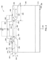
- FIG 2 is a cross-sectional view of one embodiment of the IGFET device 106.
- the IGFET device 106 includes a semiconductor body 200 that is coupled with a conductive source terminal 202 and a conductive drain terminal 204.
- the source terminal 202 may be conductively coupled with the power source 102 (shown in Figure 1 ) and the drain terminal 204 may be conductively coupled with the load 104 (shown in Figure 1 ).
- a conductive drain contact 206 is disposed along a bottom side 208 of the semiconductor body 200 with the drain terminal 204 conductively coupled with the contact 206.
- the source terminal 202 may be conductively coupled with a conductive source contact 210 disposed on a top side 212 of the semiconductor body 200 with the source terminal 202 conductively coupled with the source contact 210.
- the source contact 210 may be formed from or include one or more conductive materials, such as metals, metal alloys, polysilicon, and the like.
- the semiconductor body 200 may include, or be formed from, a doped semiconductor material, such as silicon carbide (SiC) that is doped with an n-type dopant (e.g., nitrogen or phosphorus).
- a doped semiconductor material such as silicon carbide (SiC) that is doped with an n-type dopant (e.g., nitrogen or phosphorus).
- the semiconductor body 200 may be relatively lightly doped so that the semiconductor body 200 is an n- material.
- the semiconductor body 200 may be more heavily doped and/or may be doped with a p-type dopant (e.g., aluminum or boron).
- the semiconductor body 200 is formed from another type of semiconductor material.
- the semiconductor body 200 has a doped layer 214 along the bottom side 208 of the semiconductor body 200.
- the doped layer 214 may be doped with the same type of dopant as the semiconductor body 200 (e.g., an n-type dopant) and/or may be more heavily doped than the semiconductor body 200 (e.g., an n+ material).
- the semiconductor body 200 includes doped first well regions 216 that represent volumes of the semiconductor body 200 that are doped with a different type (e.g., oppositely charged) of dopant than the semiconductor body 200.
- the first well regions 216 may be doped with a p-type dopant.
- the first well regions 216 may be disposed within the semiconductor body 200 such that the first well regions 216 include less than the entire semiconductor body 200 and the semiconductor body 216 is significantly larger (e.g., in volume) than the first well regions 216.
- the first well regions 216 are heavily doped relative to the semiconductor body 200 (e.g., the first well regions 216 may be p+ doped volumes).
- the first well regions 216 are laterally spaced apart from each other and separated from each other by a separation region 218 of the semiconductor body 200.
- the separation region 218 may be referred to as a junction gate field-effect transistor (JFET) region.
- JFET junction gate field-effect transistor
- the separation region 218 can have a width dimension 254 that laterally extends in the semiconductor body 200 from one of the first well regions 216 to the other first well region 216 shown in Figure 2 .
- the semiconductor body 200 includes doped second well regions 220 that represent volumes of the semiconductor body 200 that are doped with a different type (e.g., oppositely charged) of dopant than the first well regions 216.
- the second well regions 220 may be doped with an n-type dopant.
- the second well regions 220 are more heavily doped than the semiconductor body 200 (e.g., the second well regions 220 may be n+ doped volumes).
- the second well regions 220 may be disposed within the first well regions 216 of the semiconductor body 200 such that the second well regions 220 include less than the entire first well regions 216 and are enclosed within the first well regions 216.
- the second well regions 220 may extend into the semiconductor body 200 by a depth dimension 222 that is smaller than a depth dimension 224 that the first well regions 216 extend into the semiconductor body 200 from the top side 212 of the semiconductor body 200.
- the second well regions 220 may laterally extend in the semiconductor body 200 by a width dimension 226 that is smaller than a width dimension 228 that the first well regions 216 laterally extend in the semiconductor body 200.
- a gate dielectric 234 is disposed on the top side 212 of the semiconductor body 200.
- the gate dielectric 234 includes, or is formed from, a non-conductive material, such as silicon dioxide or some other material that does not conduct electric current.
- the gate dielectric 234 laterally extends across the top side 212 of the semiconductor body 200 between opposite ends 236, 238. In the illustrated embodiment, the opposite ends 236, 238 are disposed directly above the first and second well regions 216, 220 such that the gate oxide 234 is a continuous body extending across the separation region 218.
- the gate dielectric 234 is staged in thickness dimensions 240, 242 to form different sections 244, 246, 248.
- the gate oxide 234 may be a continuous body such that the oxide sections 244, 246, 248 are joined with each other and not separated from each other.
- Outer sections 244, 248 are disposed on opposite sides of an interior oxide section 246.
- the first outer oxide section 244 extends from the first end 236 to the interior oxide section 246 and the second outer oxide section 248 extends from the second end 238 to the interior oxide section 246.
- one or more other oxide sections having one or more other thickness dimensions may be provided.
- the interior oxide section 246 is disposed above the separation region 218 (JFET).
- the interior oxide section 246 may not extend above the first well regions 216 and may be confined to the area above the separation region 218.
- the outer oxide sections 244, 248 may be disposed above the first well regions 216 and portions of the second well regions 220.
- the thickness dimension 242 of the interior oxide section 246 is larger than the thickness dimension 240 of the outer oxide sections 244, 248 in one embodiment.
- the thickness dimension 240 of the outer oxide sections 244, 248 may be 0.05 microns (or micrometers) or less and the thickness dimension 242 of the interior oxide section 246 may be larger than 0.05 microns.
- the thickness dimension 242 may be 0.1 micron or more. In another embodiment, the thickness dimension 242 may be 0.25 micron or more. Alternatively, the thickness dimension 242 may be 0.55 micron or more.
- the thickness dimension 242 of the interior oxide section 246 can be based on the thickness dimension 240 of the outer oxide sections 244, 248. For example, the thickness dimension 242 may be an integer multiple of the thickness dimension 240, such as 2, 5, 11, or other integer multiple. Alternatively, the thickness dimension 242 may be a non-integer multiple of the thickness dimension 240.
- a conductive gate contact 250 is disposed above the gate oxide 234.
- the gate contact 250 may be formed from or include one or more conductive materials, such as metals, metal alloys, polysilicon, and the like.
- the gate contact 250 is separated from the semiconductor body 200 by the gate oxide 234.
- the gate oxide 234 prevents the gate contact 250 from engaging the semiconductor body 200.
- the gate contact 250 continuously extends across the entire gate oxide 234 in the illustrated embodiment. Alternatively, the gate contact 250 may only extend over a portion of the gate oxide 234.
- the gate contact 250 is conductively coupled with a conductive gate terminal 252.
- the gate terminal 252 may be conductively coupled with the control unit 108 (shown in Figure 1 ) such that the control unit 108 can control when an electric gate signal is applied to the gate terminal 252, as described below.
- the source terminal 202 can be conductively coupled with the power source 102 (shown in Figure 1 ) and the drain terminal 204 can be conductively coupled with the load 104 (shown in Figure 1 ).
- the IGFET device 106 When no gate signal is applied to the gate terminal 252 or a gate signal having a voltage that is lower than the turn on voltage (threshold voltage) of the IGFET device 106 is applied to the gate terminal 252, the IGFET device 106 is in a blocking or nonconductive state. When in the blocking or nonconductive state, no significant current flows through the source terminal 202 and drain terminal 204.
- the control unit 108 (shown in Figure 1 ) can be controlled to apply a gate signal having a voltage that meets or exceeds the threshold voltage of the IGFET device 106 to the gate terminal 252.
- a gate signal having a voltage that meets or exceeds the threshold voltage of the IGFET device 106 to the gate terminal 252.
- a relatively high concentration of negative charge carriers (such as electrons) in the semiconductor body 200 is attracted toward the FET channel region, the portion of 216 along the semiconductor surface.
- the negative charge carriers may be attracted from the second well regions 220.
- the relatively high concentration of the negative charge carriers forms an inversion layer in the channel region along the surface of the semiconductor body 200 between the first well regions 216 and the second well regions 220.
- the inversion layer provides a conductive channel in the semiconductor body 200 at or near the interface between the first well surface 216 and the gate dielectric 234. If the gate signal has a sufficiently large voltage, then the conductive channel formed will allow the current applied to the source terminal 202 to flow through the source contact 210 and the semiconductor body 200 (e.g., through the conductive channel) and to the drain terminal 204 through the drain contact 250.
- the gate signal When the gate signal is removed, such as by decreasing the voltage of the gate signal below the threshold voltage of the IGFET device 106, the conductive channel is no longer formed and the current may be unable to flow through the semiconductor body 200 to the drain terminal 204.
- Application of the gate signal can be used to control the flow of the current from the power source 102 (shown in Figure 1 ) to the load 104 (shown in Figure 1 ) in this way.
- the presence of the doped surface regions 230 alone may not increase the peak electric field at the SiC and SiO 2 interface.
- the doped surface regions 230 can be eliminated and the net concentration in the JFET region in reverse condition may be important, as the peak electric field under the gate oxide (e.g., at the oxide-semiconductor interface) is in the middle of JFET region.
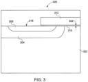
- FIG 3 is a cross-sectional view of an IGFET device 300 in accordance with one example. Similar to the IGFET device 106 shown in Figure 2 , the IGFET device 300 includes a semiconductor body 302, a first well region 304, a second well region 306, a gate oxide 310, and a conductive gate contact 250. Only part of the IGFET device 300 is shown in Figure 3 . For example, the IGFET device 300 may also include another first well region 304 and/or second well region 306, and may include a doped layer similar to the layer 214 (shown in Figure 2 ), a drain that is similar to the drain 206 (shown in Figure 2 ), and a contact similar to the source contact 210 (shown in Figure 2 ).
- the gate oxide 310 in the IGFET device 300 has a constant thickness dimension 322 of 0.05 microns in the illustrated example.
- the gate oxide 310 may not have a thicker interior section and thinner outer sections similar to the IGFET device 106 shown in Figure 2 .
- Figure 4 illustrates relationships 400, 402 between electric fields and locations in the IGFET device 300 shown in Figure 3 with the device operating in the blocking (off) state.
- the relationships 400, 402 are shown alongside the horizontal axis 314 (representative of lateral distances from the left side of the IGFET device 300) and a vertical axis 404 representative of the magnitude of the electric fields in units of 100,000 volts per centimeter (e.g., (V/cm 3 ) * 10 6 ).
- a horizontal axis 314 representative of distance from a left side of the IGFET device 300 and a vertical axis 316 representative of distance from a top side 318 of the semiconductor body 302 are shown.
- the relationship 400 represents the magnitude of the electric field in the semiconductor body 302 at the different lateral distances of the horizontal axis 314.
- the relationship 402 represents the magnitude of the electric field in the gate oxide 310 at the different lateral distances of the horizontal axis 314.
- the electric field in the gate oxide 310 is smaller than in the semiconductor body 302 at lateral distances from the left side of the IGFET device 300 up to the interface between the first well region 304 and the remainder of the semiconductor body 302 (e.g., at approximately 3.05 microns).
- the electric field in the gate oxide 310 is larger.
- the electric field in the gate oxide 402 approaches a value of 4020000 V/cm 3 (e.g., at lateral distances of 5.08 microns or more).
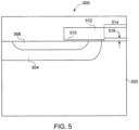
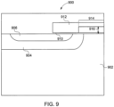
- FIGS 5 , 7 , and 9 illustrate cross-sectional views of IGFET devices 500, 700, 900 in accordance with additional examples. Similar to the IGFET device 106 shown in Figure 2 , the IGFET devices 500, 700, 900 include semiconductor bodies 502, 702, 902, first well regions 504, 704, 904, second well regions 506, 706, 906, gate oxides 510, 710, 910, and conductive contacts 512, 712, 912. Only parts of the IGFET devices 500, 700, 900 are shown in Figures 5 , 7 , and 9 .
- the IGFET devices 500, 700, 900 may also include additional first well regions 504, 704, 904 and/or second well regions 506, 706, 906, and may include doped layers similar to the layer 214 (shown in Figure 2 ), cathodes that are similar to the cathode 206 (shown in Figure 2 ), and contacts similar to the source contact 210 (shown in Figure 2 ).
- the gate oxides 510, 710, 910 have shapes that are similar to the gate oxide 234 shown in Figure 2 .
- the gate oxides 510, 710, 910 have thicker interior sections 514, 714, 914 than other sections (e.g., outer sections) of the gate oxides 510, 710, 910.
- the gate oxides 510, 710, 910 have thickness dimensions 516, 716, 916 in the interior sections 514, 714, 914 of 0.1 microns, 0.25 microns, and 0.55 microns, respectively.
- other thickness dimensions 516, 716, 916 may be used.
- the horizontal axis 314 representative of distance from left sides of the IGFET devices 500, 700, 900 is shown in Figures 5 , 7 , and 9 , as well as the vertical axis 316 representative of distance from top sides of the semiconductor bodies 502, 702, 900.
- Figures 6 , 8 , and 10 illustrate relationship between electric fields and locations in the IGFET devices 500, 700, 900 shown in Figures 5 , 7 , and 9 , respectively.
- Figure 6 illustrates relationships 600, 602 for the IGFET device 500
- Figure 8 illustrates relationships 800, 802 for the IGFET device 700
- Figure 10 illustrates relationships 1000, 1002 for the IGFET device 900.
- the relationships 600, 800, 1000 represent the magnitudes of the electric fields in the semiconductor bodies 502, 702, 902 at the different lateral distances of the horizontal axis 314.
- the relationships 602, 802, 1002 represent the magnitudes of the electric fields in the gate oxides 510, 710, 910 at the different lateral distances of the horizontal axis 314.
- the electric fields in the gate oxides 310, 510, 710, 910 decrease with increasing thickness dimensions of the interior sections of the gate oxides.
- the electric field in the gate oxide 310 approaches a value of 4,020,000 V/cm 3
- the electric field in the gate oxide 510 approaches a value of 4,000,000 V/cm 3
- the electric field in the gate oxide 710 approaches a value of 3,040,000 V/cm 3
- the electric field in the gate oxide 910 approaches a value of just over 2,250,000 V/cm 3 .
- the thickness dimensions 322, 516, 716, 916 associated with the interior sections of the gate oxides 310, 510, 710, 910 are 0.05 microns, 0.1 microns, 0.25 microns, and 0.55 microns, respectively.
- Other decreases in the electric fields within the gate oxides may be realized with other thickness dimensions of the interior section.
- a thickness dimension for the interior section of a gate oxide may be increased to 0.4 microns such that the electric field in the gate oxide approaches a value of 3,750,000 V/cm 3 .
- increasing the thickness dimension of the interior section of a gate oxide in the IGFET device can result in decreasing electric fields in the gate oxide when the dopant concentration in the first well regions are increased and/or the doped surface region is provided in the IGFET device relative to conventional IGFET devices, as described above. Also as described above, reducing the electric fields in the gate oxide can increase the useful life or life span of the IGFET device.
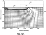
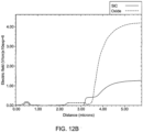
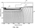
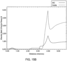
- Figures 12 through 16 show the effect of increasingly thicker oxides over the JFET region on oxide electric field at 6.5 kV.
- Figures 12A , 13A , 14A , 15A , and 16A show cross-sectional views of different embodiments of the IGFET devices having different oxide thicknesses (t JFET ox) over the JFET region.
- Figures 12B , 13B , 14B , 15B , and 16B show the electric fields along the SiC-SiO 2 interfaces of the devices shown in the corresponding Figures 12A , 13A , 14A , 15A , and 16A .
- the oxide thickness over the JFET region in Figure 12A is 0.05 ⁇ m, 0.1 ⁇ m in Figure 13A , 0.15 ⁇ m in Figure 14A , 0.25 ⁇ m in Figure 15A , and 0.55 ⁇ m in Figure 16A .
- Thicker oxides reduce the center electric field, but at the expense of the electric field at the transition edge between the thinner oxide portion and the thicker oxide portion.
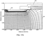
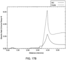
- Figures 17 through 20 show the effect of oxide taper angles and oxide thickness, while keeping the electric field below 4.0 Mv/cm.
- Figures 17A , 18A , 19A , and 20A show cross-sectional views of different embodiments of the IGFET devices having different oxide taper angles.
- the oxide thickness (t JFET ox) over the JFET region is 0.55 ⁇ m in Figures 17A , 18A , and 19A and is 0.2 ⁇ m in Figure 20A .
- the oxide taper angle is approximately 90 degrees in Figure 17A , approximately 45 degrees in Figures 18A and 20A , and is approximately 17 degrees in Figure 19A .
- the oxide taper angle may be between 75 and 105 degrees, between 30 and 50 degrees, or between 10 and 30 degrees.
- Figures 17B , 18B , 19B , and 20B show the electric fields along the SiC-SiO 2 interfaces of the devices shown in the corresponding Figures 17A , 18A , 19A , and 20A .
- Figures 18A and 18B show further optimization of thickness and taper angles of the oxide, with a 6 degree taper providing an improved solution in one embodiment.
- the electric field in SiO 2 can be effectively reduced by increasing the thickness of oxide above JFET region up to 0.5 ⁇ m as shown in Figures 12 through 16 , while not compromising the on-state resistance of the device by not having any of the thicker portion of the gate oxide over the conduction channel (p-well region). It should be noted, that despite the electric field being decreased below 3MV/cm in the center of JFET region, its value can increase up to 6MV/cm near the corner of thick oxide region due to field crowding. This would exceed reliability requirements that the electric field be less than or equal to 4MV/cm.
- the additional optimization of oxide thickness indicates that the 0.15 ⁇ m of SiO 2 provides the same electric field value in the center of JFET region and near the corner of thick oxide region ( ⁇ 3.8MV/cm).
- Additional suppression of electric field near the corner of thick oxide can be obtained by sloping the oxide (e.g., by providing a beveled structure).
- the beveled 0.5 ⁇ m oxide having an angle of approximately 17 degrees allows the corner electric field to be reduced from 6 MV/cm to 4.5 MV/cm.
- Further optimization of the oxide thickness and bevel angle are shown in Figures 18A and 18B , where it is shown that bevel angles can reduce the peak JFET electric field, which occurs at the thin to thick oxide transition edge on the non-beveled example.
- the embodiments shown in Figure 14 have electric fields of less than 4.0 MV/cm.
- FIG 11 is a flowchart of one embodiment of a method 1100 for providing an IGFET device.
- the method 1100 may be used to create one or more of the IGFET devices described herein, such as the IGFET devices 106, 500, 700, and/or 900 shown in Figures 1 , 5 , 7 , and 9 . While reference is made herein to the components of the IGFET device 106 shown in Figure 2 , the discussion may equally apply to the similar or same components of the other IGFET devices 500, 700, 900 shown and described herein.
- a semiconductor body is provided.
- a layer of a semiconductive material such as SiC
- the layer may be a layer that is deposited or epitaxially grown on a substrate, or may be provided as a semiconductor wafer.
- the semiconductor body is doped, such as with an n-type dopant.
- the semiconductor body may be relatively lightly doped so that the semiconductor body is an n- doped body.
- a p-type dopant may be used.
- the semiconductor body may include a doped layer at or near a side of the semiconductor body where a conductive drain will be joined.
- the layer 214 is typically formed when the body layer 200 is epitaxially grown on a heavily doped substrate 214.
- first well regions are formed in the semiconductor body.
- the first well regions 216 may be formed by doping the corresponding volumes of the semiconductor body 200.
- the first well regions 216 are formed by covering the volumes of the semiconductor body 200 with a removable mask (e.g., using photolithography) and diffusing and/or ion implanting the dopants into the first well regions 216. The removable mask is then removed from the semiconductor body 200.
- the first well regions 216 may be formed using a dopant that is oppositely charged from the dopant in the semiconductor body 200.
- the semiconductor body 200 is doped with an n-type dopant
- the first well regions 216 may be formed using a p-type dopant.
- the semiconductor body 200 is doped with a p-type dopant
- the first well regions 216 may be formed using an n-type dopant.
- the first well regions 216 may be significantly more heavily doped than the semiconductor body 200.
- the first well regions 216 may be more heavily doped when the first well regions 216 have a concentration of dopants that is at least one order of magnitude (e.g., 10 times greater) than the concentration of dopants in the semiconductor body 200.
- the first well regions 216 may be more heavily doped when the first well regions 216 have a concentration of dopants that is at least two orders of magnitude (e.g., 100 times greater) than the concentration of dopants in the semiconductor body 200.
- the first well regions 216 may be more heavily doped when the first well regions 216 have a concentration of dopants that is at least three orders of magnitude (e.g., 1,000 times greater) than the concentration of dopants in the semiconductor body 200. However, other different orders of magnitude in the difference of the dopant concentrations may be used.
- second well regions are formed in the semiconductor body.
- the second well regions 220 may be formed by doping the corresponding volumes of the semiconductor body 200 inside the first well regions 216.
- the second well regions 220 can be formed by covering the volumes of the semiconductor body 200 with a removable mask (e.g., using photolithography) and diffusing and/or ion implanting the dopants into the second well regions 220. The removable mask is then removed from the semiconductor body 200.
- the second well regions 220 may be formed using a dopant that is oppositely charged from the dopant in the first semiconductor regions 216.
- the first well regions 216 are doped with a p-type dopant
- the second well regions 220 may be formed using an n-type dopant.
- the second well regions 220 may be formed using a p-type dopant.
- a gate dielectric is grown or deposited (or both) onto the semiconductor body.
- the gate oxide 234 may be deposited by covering portions of the semiconductor body 200 where the gate oxide 234 will not be present (e.g., using photolithography) and growing a dielectric layer (e.g., a layer of silicon dioxide) on the exposed portions of the semiconductor body 200.
- a removable mask may be deposited onto the semiconductor body 200 and growing the thinner outer portions 244, 248 and a first part of the interior portion 246 on the areas of the semiconductor body 200 that are exposed by the mask.
- the mask may be removed and another removable mask may be provided that covers the outer portions 244, 248 of the gate oxide 234 while exposing the interior portion 246.
- the remaining thickness of the interior portion 246 of the gate oxide 234 can then be grown and the mask can be removed.
- conductive contacts are deposited onto the semiconductor body.
- the gate contact 250, the source contact 210, and the drain contact 206 may be provided.
- the drain contact 206 may be provided by sputtering or otherwise depositing one or more metals, metal alloys, polysilicon materials, and the like, onto the bottom side 208 of the semiconductor body 200.
- the source contact 210 and/or the gate contact 250 may be formed by forming a removable mask on the semiconductor body 200 (e.g., using photolithography) and sputtering or otherwise depositing one or more metals, metal alloys, polysilicon materials, and the like, onto the top side 212 of the semiconductor body 200. The removable mask may then be removed.
- the source contact 210 may be conductively coupled with a source of electric current
- the drain contact 204 may be conductively coupled with an electric load
- the gate contact 250 can be conductively coupled with a control unit that controls when a gate signal is applied to the gate contact 250, as described above.
Landscapes
- Insulated Gate Type Field-Effect Transistor (AREA)
- Metal-Oxide And Bipolar Metal-Oxide Semiconductor Integrated Circuits (AREA)
- Junction Field-Effect Transistors (AREA)
Abstract
Description
- Metal-oxide-semiconductor field effect transistor (MOSFET) devices are used to switch the flow of current in a circuit between conducting and non-conducting states. The MOSFET devices include doped source and drain regions in a semiconductor with a gate oxide disposed over the semiconductor between the source and drain regions. The source regions are disposed within larger doped well regions with the source region being doped with an oppositely charged dopant than the well region. A gate contact is disposed over the gate oxide and separated from the semiconductor by the gate oxide. An electronic signal is applied to the gate contact to create a conductive path through the semiconductor from the source to the drain regions. When the signal is removed from the gate contact, the conductive path is no longer present and the semiconductor prevents current from flowing through the semiconductor.
- The semiconductor of the MOSFET device may be associated with an on-resistance characteristic that represents the electrical resistance of the MOSFET device to switching from a non-conducting state to the conducting state. This on-resistance characteristic can be reduced in order to decrease power dissipation losses of the MOSFET device. However, decreasing the on-resistance characteristic may be accomplished by reducing the FET channel, connecting source to drain, which can lead to punch through breakdown. Additionally, punch through may result in an increase in the output conductance of the MOSFET device and a decrease in an upper limit on the operating voltage of the MOSFET device.
- In order to reduce the potential for punch through to occur, the dopant concentration of the well regions in the semiconductor may be increased. However, such an increase in the dopant concentration can result in an increase in the voltage needed in the signal applied to the gate contact to switch the MOSFET device from the non-conducting state to the conducting state. During the non-conducting state, the gate will be biased below the threshold value required for channel conduction and is usually at the same potential as the source or below (e.g. a negative gate bias value for an N-channel FET). When the device is in its full blocking state, the depletion charge on the lightly doped side of the blocking junction creates an electric field which penetrates the separations in the blocking junction to the interface, and will terminate on the gate electrode. The ratio of dielectric constants between the semiconductor and the gate oxide will amplify the electric field strength component normal to the surface [e.g. Eox = (εSiC / εox)∗ Esic ], by the ratios of the relative permittivities. For the case of a SiC and silicon oxide interface, the normal field is enhanced by a factor 2.5 in the oxide. As the electric fields generated in the gate oxide increase, the reliability and/or useful life of the MOSFET device can decrease due to breakdown in the gate oxide material. Thus it is desirable to reduce the field strength in the gate oxide which covers the spaces between the blocking junctions, commensurate with proper FET operation in the conducting channel.
- In one embodiment, an insulating gate field effect transistor (IGFET) device is provided that includes a semiconductor body and a gate oxide. The semiconductor body is conductively coupled with a source contact and a drain contact. The semiconductor body includes a first well region comprising a first volume of the semiconductor body that is disposed at a first side of the semiconductor body and that is doped with a first type of dopant. The semiconductor body also includes a second well region comprising a second volume of the semiconductor body that is disposed at the first side of the semiconductor body and that is doped with an oppositely charged second type of dopant. The second well region is disposed within the first well region. The gate oxide is coupled with the semiconductor body and with a gate contact. The gate oxide includes an outer section and an interior section having different thickness dimensions. The outer section is disposed over the first well region and the second well region of the semiconductor body. The interior section is disposed over a junction gate field effect transistor region of the semiconductor body. The semiconductor body is configured to form a conductive channel from the source contact to the drain contact through the second well region and the junction gate field effect transistor region when a gate signal is applied to the gate contact.
- In another embodiment, a method is provided that includes doping a semiconductor body with a first type of dopant in a first volume of the semiconductor body to form a first well region and doping the semiconductor body with an oppositely charged second type of dopant in a second volume of the semiconductor body to form a second well region. The second well region is disposed within the first well region. The method also includes providing a gate oxide on the semiconductor body. The gate oxide includes an outer section with thickness equal to or thicker than the interior section. The outer section is disposed over the first well region and the second well region of the semiconductor body. The interior section is disposed over a junction gate field effect transistor region of the semiconductor body. The method further includes conductively coupling a source contact with at least one of the first well region or the second well region of the semiconductor body, a drain contact with the semiconductor body, and a gate contact with the gate oxide. The semiconductor body is configured to form a conductive channel from the source contact to the drain contact through the second well region and the junction gate field effect transistor region when a gate signal is applied to the gate contact.
- In another embodiment, another IGFET device is provided that includes a semiconductor body and a gate oxide. The semiconductor body has first well regions doped with a first type of dopant and second well regions doped with an oppositely charged second type of dopant. The second well regions are disposed in the first well regions. The first well regions are separated from each other by a junction gate field effect transistor region of the semiconductor body. The semiconductor body is configured to be conductively coupled with a drain contact and at least one of the first well regions or the second well regions configured to be conductively coupled with a source contact. The gate oxide is disposed over the semiconductor body and is configured to be conductively coupled with a gate contact. The gate oxide has an interior section disposed over the junction gate field effect transistor region of the semiconductor body and outer sections at least partially disposed over the first well regions. The interior section of the gate oxide has a first thickness dimension that is equal to or thicker than the outer section.
- The inventive subject matter will be better understood from reading the following description of non-limiting embodiments, with reference to the attached drawings, wherein below:
-
Figure 1 is a block diagram of one embodiment of a switching system; -
Figure 2 is a cross-sectional view of one embodiment of an insulating gate field effect transistor (IGFET) device shown inFigure 1 ; -
Figure 3 is a cross-sectional view of an IGFET device in accordance with one example; -
Figure 4 illustrates relationships between electric fields and locations in the IGFET device shown inFigure 3 ; -
Figure 5 illustrates a cross-sectional view of an IGFET device in accordance with another example; -
Figure 6 illustrates a relationship between electric fields and locations in the IGFET device shown inFigure 5 ; -
Figure 7 illustrates a cross-sectional view of an IGFET device in accordance with another example; -
Figure 8 illustrates a relationship between electric fields and locations in the IGFET device shown inFigure 7 ; -
Figure 9 illustrates a cross-sectional view of an IGFET device in accordance with another example; -
Figure 10 illustrates a relationship between electric fields and locations in the IGFET device shown inFigure 9 ; -
Figure 11 is a flowchart of one embodiment of a method for providing an IGFET device; -
Figure 12A illustrates a cross-sectional view of an IGFET device having an oxide thickness over a JFET region of 0.05 µm in accordance with one embodiment; -
Figure 12B illustrates an electric field along an SiC-SiO2 interface of the device shown inFigure 12A ; -
Figure 13A illustrates a cross-sectional view of an IGFET device having an oxide thickness over a JFET region of 0.1 µm in accordance with one embodiment; -
Figure 13B illustrates an electric field along an SiC-SiO2 interface of the device shown inFigure 13A ; -
Figure 14A illustrates a cross-sectional view of an IGFET device having an oxide thickness over a JFET region of 0.15 µm in accordance with one embodiment; -
Figure 14B illustrates an electric field along an SiC-SiO2 interface of the device shown inFigure 14A ; -
Figure 15A illustrates a cross-sectional view of an IGFET device having an oxide thickness over a JFET region of 0.25 µm in accordance with one embodiment; -
Figure 15B illustrates an electric field along an SiC-SiO2 interface of the device shown inFigure 15A ; -
Figure 16A illustrates a cross-sectional view of an IGFET device having an oxide thickness over a JFET region of 0.55 µm in accordance with one embodiment; -
Figure 16B illustrates an electric field along an SiC-SiO2 interface of the device shown inFigure 16A ; -
Figure 17A illustrates a cross-sectional view of an IGFET device having an oxide thickness over a JFET region of 0.55 µm and an oxide taper angle of 90 degrees in accordance with one embodiment; -
Figure 17B illustrates an electric field along an SiC-SiO2 interface of the device shown inFigure 17A ; -
Figure 18A illustrates a cross-sectional view of an IGFET device having an oxide thickness over a JFET region of 0.55 µm and an oxide taper angle of 45 degrees in accordance with one embodiment; -
Figure 18B illustrates an electric field along an SiC-SiO2 interface of the device shown inFigure 18A ; -
Figure 19A illustrates a cross-sectional view of an IGFET device having an oxide thickness over a JFET region of 0.55 µm and an oxide taper angle of approximately 17 degrees in accordance with one embodiment; -
Figure 19B illustrates an electric field along an SiC-SiO2 interface of the device shown inFigure 19A ; -
Figure 20A illustrates a cross-sectional view of an IGFET device having an oxide thickness over a JFET region of 0.2 µm and an oxide taper angle of approximately 45 degrees in accordance with one embodiment; and -
Figure 20B illustrates an electric field along an SiC-SiO2 interface of the device shown inFigure 20A . - Reference will be made below in detail to example embodiments of the inventive subject matter, examples of which are illustrated in the accompanying drawings. Wherever possible, the same reference numerals used throughout the drawings refer to the same or like parts. At least one embodiment described herein provides for a power insulated-gate field-effect transistor (IGFET) device, such as a metal-oxide-semiconductor field-effect transistor (MOSFET), that may be used as or in a switch to control the flow of relatively high currents to one or more loads. While the description herein provides examples of materials that may be used to form the IGFET device, alternatively, one or more other materials may be used.
-
Figure 1 is a block diagram of one embodiment of aswitching system 100. Theswitching system 100 may be used to control the flow of electric current from a power source 102 (e.g., power grid, wind turbine, photovoltaic device, battery, and the like) to an electric load 104 (e.g., an electric motor or other device that performs work when electric current is received or stores the electric current for later use). Theswitching system 100 includes at least one IGFET device 106 ("Controlled Switch" inFigure 1 ) that is conductively coupled with thepower source 102 and theload 104. TheIGFET device 106 is communicatively coupled (e.g., coupled by one or more wired and/or wireless connections) with acontrol unit 108. Thecontrol unit 108 can include a processor, controller, or other logic-based device that automatically switches or is manually controlled to switch theIGFET device 106 between an ON, conducting, or an OFF closed state. TheIGFET device 106 is in the ON state to allow the current from thepower source 102 to be conducted through theIGFET device 106 to theload 104. TheIGFET device 106 is in the OFF state to block the flow of the current through theIGFET device 106 from thepower source 102 to theload 104. -
Figure 2 is a cross-sectional view of one embodiment of theIGFET device 106. TheIGFET device 106 includes asemiconductor body 200 that is coupled with aconductive source terminal 202 and aconductive drain terminal 204. Thesource terminal 202 may be conductively coupled with the power source 102 (shown inFigure 1 ) and thedrain terminal 204 may be conductively coupled with the load 104 (shown inFigure 1 ). In the illustrated embodiment, aconductive drain contact 206 is disposed along abottom side 208 of thesemiconductor body 200 with thedrain terminal 204 conductively coupled with thecontact 206. Thesource terminal 202 may be conductively coupled with aconductive source contact 210 disposed on atop side 212 of thesemiconductor body 200 with thesource terminal 202 conductively coupled with thesource contact 210. Thesource contact 210 may be formed from or include one or more conductive materials, such as metals, metal alloys, polysilicon, and the like. - The
semiconductor body 200 may include, or be formed from, a doped semiconductor material, such as silicon carbide (SiC) that is doped with an n-type dopant (e.g., nitrogen or phosphorus). Thesemiconductor body 200 may be relatively lightly doped so that thesemiconductor body 200 is an n- material. Alternatively, thesemiconductor body 200 may be more heavily doped and/or may be doped with a p-type dopant (e.g., aluminum or boron). In another embodiment, thesemiconductor body 200 is formed from another type of semiconductor material. - In the illustrated embodiment, the
semiconductor body 200 has a dopedlayer 214 along thebottom side 208 of thesemiconductor body 200. The dopedlayer 214 may be doped with the same type of dopant as the semiconductor body 200 (e.g., an n-type dopant) and/or may be more heavily doped than the semiconductor body 200 (e.g., an n+ material). - The
semiconductor body 200 includes doped first wellregions 216 that represent volumes of thesemiconductor body 200 that are doped with a different type (e.g., oppositely charged) of dopant than thesemiconductor body 200. For example, the firstwell regions 216 may be doped with a p-type dopant. As shown inFigure 2 , the firstwell regions 216 may be disposed within thesemiconductor body 200 such that the firstwell regions 216 include less than theentire semiconductor body 200 and thesemiconductor body 216 is significantly larger (e.g., in volume) than the firstwell regions 216. - In one embodiment, the first
well regions 216 are heavily doped relative to the semiconductor body 200 (e.g., the firstwell regions 216 may be p+ doped volumes). The firstwell regions 216 are laterally spaced apart from each other and separated from each other by aseparation region 218 of thesemiconductor body 200. Theseparation region 218 may be referred to as a junction gate field-effect transistor (JFET) region. Theseparation region 218 can have awidth dimension 254 that laterally extends in thesemiconductor body 200 from one of the firstwell regions 216 to the other firstwell region 216 shown inFigure 2 . - The
semiconductor body 200 includes doped second wellregions 220 that represent volumes of thesemiconductor body 200 that are doped with a different type (e.g., oppositely charged) of dopant than the firstwell regions 216. For example, the secondwell regions 220 may be doped with an n-type dopant. In one embodiment, the secondwell regions 220 are more heavily doped than the semiconductor body 200 (e.g., the secondwell regions 220 may be n+ doped volumes). - As shown in
Figure 2 , the secondwell regions 220 may be disposed within the firstwell regions 216 of thesemiconductor body 200 such that the secondwell regions 220 include less than the entire firstwell regions 216 and are enclosed within the firstwell regions 216. The secondwell regions 220 may extend into thesemiconductor body 200 by adepth dimension 222 that is smaller than adepth dimension 224 that the firstwell regions 216 extend into thesemiconductor body 200 from thetop side 212 of thesemiconductor body 200. The secondwell regions 220 may laterally extend in thesemiconductor body 200 by awidth dimension 226 that is smaller than awidth dimension 228 that the firstwell regions 216 laterally extend in thesemiconductor body 200. - A
gate dielectric 234 is disposed on thetop side 212 of thesemiconductor body 200. Thegate dielectric 234 includes, or is formed from, a non-conductive material, such as silicon dioxide or some other material that does not conduct electric current. Thegate dielectric 234 laterally extends across thetop side 212 of thesemiconductor body 200 between opposite ends 236, 238. In the illustrated embodiment, the opposite ends 236, 238 are disposed directly above the first and secondwell regions gate oxide 234 is a continuous body extending across theseparation region 218. - The
gate dielectric 234 is staged inthickness dimensions different sections gate oxide 234 may be a continuous body such that theoxide sections Outer sections interior oxide section 246. The firstouter oxide section 244 extends from thefirst end 236 to theinterior oxide section 246 and the secondouter oxide section 248 extends from thesecond end 238 to theinterior oxide section 246. Alternatively, one or more other oxide sections having one or more other thickness dimensions may be provided. - In the illustrated embodiment, the
interior oxide section 246 is disposed above the separation region 218 (JFET). For example, theinterior oxide section 246 may not extend above the firstwell regions 216 and may be confined to the area above theseparation region 218. Theouter oxide sections well regions 216 and portions of the secondwell regions 220. Thethickness dimension 242 of theinterior oxide section 246 is larger than thethickness dimension 240 of theouter oxide sections thickness dimension 240 of theouter oxide sections thickness dimension 242 of theinterior oxide section 246 may be larger than 0.05 microns. In one embodiment, thethickness dimension 242 may be 0.1 micron or more. In another embodiment, thethickness dimension 242 may be 0.25 micron or more. Alternatively, thethickness dimension 242 may be 0.55 micron or more. Thethickness dimension 242 of theinterior oxide section 246 can be based on thethickness dimension 240 of theouter oxide sections thickness dimension 242 may be an integer multiple of thethickness dimension 240, such as 2, 5, 11, or other integer multiple. Alternatively, thethickness dimension 242 may be a non-integer multiple of thethickness dimension 240. - A
conductive gate contact 250 is disposed above thegate oxide 234. Thegate contact 250 may be formed from or include one or more conductive materials, such as metals, metal alloys, polysilicon, and the like. Thegate contact 250 is separated from thesemiconductor body 200 by thegate oxide 234. Thegate oxide 234 prevents thegate contact 250 from engaging thesemiconductor body 200. Thegate contact 250 continuously extends across theentire gate oxide 234 in the illustrated embodiment. Alternatively, thegate contact 250 may only extend over a portion of thegate oxide 234. Thegate contact 250 is conductively coupled with aconductive gate terminal 252. Thegate terminal 252 may be conductively coupled with the control unit 108 (shown inFigure 1 ) such that thecontrol unit 108 can control when an electric gate signal is applied to thegate terminal 252, as described below. - In operation, the
source terminal 202 can be conductively coupled with the power source 102 (shown inFigure 1 ) and thedrain terminal 204 can be conductively coupled with the load 104 (shown inFigure 1 ). When no gate signal is applied to thegate terminal 252 or a gate signal having a voltage that is lower than the turn on voltage (threshold voltage) of theIGFET device 106 is applied to thegate terminal 252, theIGFET device 106 is in a blocking or nonconductive state. When in the blocking or nonconductive state, no significant current flows through thesource terminal 202 anddrain terminal 204. The control unit 108 (shown inFigure 1 ) can be controlled to apply a gate signal having a voltage that meets or exceeds the threshold voltage of theIGFET device 106 to thegate terminal 252. When such a gate signal is applied, a relatively high concentration of negative charge carriers (such as electrons) in thesemiconductor body 200 is attracted toward the FET channel region, the portion of 216 along the semiconductor surface. The negative charge carriers may be attracted from the secondwell regions 220. - The relatively high concentration of the negative charge carriers forms an inversion layer in the channel region along the surface of the
semiconductor body 200 between the firstwell regions 216 and the secondwell regions 220. The inversion layer provides a conductive channel in thesemiconductor body 200 at or near the interface between thefirst well surface 216 and thegate dielectric 234. If the gate signal has a sufficiently large voltage, then the conductive channel formed will allow the current applied to thesource terminal 202 to flow through thesource contact 210 and the semiconductor body 200 (e.g., through the conductive channel) and to thedrain terminal 204 through thedrain contact 250. When the gate signal is removed, such as by decreasing the voltage of the gate signal below the threshold voltage of theIGFET device 106, the conductive channel is no longer formed and the current may be unable to flow through thesemiconductor body 200 to thedrain terminal 204. Application of the gate signal can be used to control the flow of the current from the power source 102 (shown inFigure 1 ) to the load 104 (shown inFigure 1 ) in this way. - In one embodiment, the presence of the doped
surface regions 230 alone may not increase the peak electric field at the SiC and SiO2 interface. The dopedsurface regions 230 can be eliminated and the net concentration in the JFET region in reverse condition may be important, as the peak electric field under the gate oxide (e.g., at the oxide-semiconductor interface) is in the middle of JFET region. -
Figure 3 is a cross-sectional view of anIGFET device 300 in accordance with one example. Similar to theIGFET device 106 shown inFigure 2 , theIGFET device 300 includes asemiconductor body 302, afirst well region 304, asecond well region 306, agate oxide 310, and aconductive gate contact 250. Only part of theIGFET device 300 is shown inFigure 3 . For example, theIGFET device 300 may also include anotherfirst well region 304 and/orsecond well region 306, and may include a doped layer similar to the layer 214 (shown inFigure 2 ), a drain that is similar to the drain 206 (shown inFigure 2 ), and a contact similar to the source contact 210 (shown inFigure 2 ). - The
gate oxide 310 in theIGFET device 300 has aconstant thickness dimension 322 of 0.05 microns in the illustrated example. For example, thegate oxide 310 may not have a thicker interior section and thinner outer sections similar to theIGFET device 106 shown inFigure 2 . - With continued reference to
Figure 3 ,Figure 4 illustratesrelationships IGFET device 300 shown inFigure 3 with the device operating in the blocking (off) state. Therelationships vertical axis 404 representative of the magnitude of the electric fields in units of 100,000 volts per centimeter (e.g., (V/cm3) * 106). Ahorizontal axis 314 representative of distance from a left side of theIGFET device 300 and a vertical axis 316 representative of distance from atop side 318 of thesemiconductor body 302 are shown. - The
relationship 400 represents the magnitude of the electric field in thesemiconductor body 302 at the different lateral distances of thehorizontal axis 314. Therelationship 402 represents the magnitude of the electric field in thegate oxide 310 at the different lateral distances of thehorizontal axis 314. As shown inFigure 4 , the electric field in thegate oxide 310 is smaller than in thesemiconductor body 302 at lateral distances from the left side of theIGFET device 300 up to the interface between thefirst well region 304 and the remainder of the semiconductor body 302 (e.g., at approximately 3.05 microns). At lateral distances that are greater than this interface, the electric field in thegate oxide 310 is larger. In the model results illustrated the electric field in thegate oxide 402 approaches a value of 4020000 V/cm3 (e.g., at lateral distances of 5.08 microns or more). -
Figures 5 ,7 , and9 illustrate cross-sectional views ofIGFET devices IGFET device 106 shown inFigure 2 , theIGFET devices semiconductor bodies regions well regions gate oxides conductive contacts IGFET devices Figures 5 ,7 , and9 . For example, theIGFET devices well regions well regions Figure 2 ), cathodes that are similar to the cathode 206 (shown inFigure 2 ), and contacts similar to the source contact 210 (shown inFigure 2 ). - The
gate oxides gate oxide 234 shown inFigure 2 . For example, thegate oxides interior sections gate oxides gate oxides thickness dimensions interior sections other thickness dimensions - The
horizontal axis 314 representative of distance from left sides of theIGFET devices Figures 5 ,7 , and9 , as well as the vertical axis 316 representative of distance from top sides of thesemiconductor bodies - With continued reference to
Figures 5 ,7 , and9 ,Figures 6 ,8 , and10 illustrate relationship between electric fields and locations in theIGFET devices Figures 5 ,7 , and9 , respectively. For example,Figure 6 illustratesrelationships IGFET device 500,Figure 8 illustratesrelationships IGFET device 700, andFigure 10 illustratesrelationships IGFET device 900. - The relationships shown in
Figures 6 ,8 , and10 are shown alongside the horizontal axis 314 (representative of lateral distances from the left side of the corresponding IGFET device) and thevertical axis 404 representative of the magnitude of the electric fields in units of 100,000 volts per centimeter (e.g., (V/cm3) * 106). - The
relationships semiconductor bodies horizontal axis 314. Therelationships gate oxides horizontal axis 314. As shown inFigures 4 ,6 ,8 , and10 , the electric fields in thegate oxides gate oxide 310 approaches a value of 4,020,000 V/cm3, the electric field in thegate oxide 510 approaches a value of 4,000,000 V/cm3, the electric field in thegate oxide 710 approaches a value of 3,040,000 V/cm3, and the electric field in thegate oxide 910 approaches a value of just over 2,250,000 V/cm3. - As described above, the
thickness dimensions gate oxides -
Figures 12 through 16 show the effect of increasingly thicker oxides over the JFET region on oxide electric field at 6.5 kV.Figures 12A ,13A ,14A ,15A , and16A show cross-sectional views of different embodiments of the IGFET devices having different oxide thicknesses (tJFET ox) over the JFET region.Figures 12B ,13B ,14B ,15B , and16B show the electric fields along the SiC-SiO2 interfaces of the devices shown in the correspondingFigures 12A ,13A ,14A ,15A , and16A . The oxide thickness over the JFET region inFigure 12A is 0.05 µm, 0.1 µm inFigure 13A , 0.15 µm inFigure 14A , 0.25 µm inFigure 15A , and 0.55 µm inFigure 16A . Thicker oxides reduce the center electric field, but at the expense of the electric field at the transition edge between the thinner oxide portion and the thicker oxide portion. -
Figures 17 through 20 show the effect of oxide taper angles and oxide thickness, while keeping the electric field below 4.0 Mv/cm.Figures 17A ,18A ,19A , and20A show cross-sectional views of different embodiments of the IGFET devices having different oxide taper angles. The oxide thickness (tJFET ox) over the JFET region is 0.55 µm inFigures 17A ,18A , and19A and is 0.2 µm inFigure 20A . The oxide taper angle is approximately 90 degrees inFigure 17A , approximately 45 degrees inFigures 18A and20A , and is approximately 17 degrees inFigure 19A . In another embodiment, the oxide taper angle may be between 75 and 105 degrees, between 30 and 50 degrees, or between 10 and 30 degrees. -
Figures 17B ,18B ,19B , and20B show the electric fields along the SiC-SiO2 interfaces of the devices shown in the correspondingFigures 17A ,18A ,19A , and20A . In one embodiment,Figures 18A and18B show further optimization of thickness and taper angles of the oxide, with a 6 degree taper providing an improved solution in one embodiment. - The electric field in SiO2 can be effectively reduced by increasing the thickness of oxide above JFET region up to 0.5 µm as shown in
Figures 12 through 16 , while not compromising the on-state resistance of the device by not having any of the thicker portion of the gate oxide over the conduction channel (p-well region). It should be noted, that despite the electric field being decreased below 3MV/cm in the center of JFET region, its value can increase up to 6MV/cm near the corner of thick oxide region due to field crowding. This would exceed reliability requirements that the electric field be less than or equal to 4MV/cm. The additional optimization of oxide thickness indicates that the 0.15 µm of SiO2 provides the same electric field value in the center of JFET region and near the corner of thick oxide region (~3.8MV/cm). - Additional suppression of electric field near the corner of thick oxide can be obtained by sloping the oxide (e.g., by providing a beveled structure). As shown in
Figures 19A and19B , the beveled 0.5 µm oxide having an angle of approximately 17 degrees allows the corner electric field to be reduced from 6 MV/cm to 4.5 MV/cm. Further optimization of the oxide thickness and bevel angle are shown inFigures 18A and18B , where it is shown that bevel angles can reduce the peak JFET electric field, which occurs at the thin to thick oxide transition edge on the non-beveled example. The embodiments shown inFigure 14 have electric fields of less than 4.0 MV/cm. -
Figure 11 is a flowchart of one embodiment of amethod 1100 for providing an IGFET device. Themethod 1100 may be used to create one or more of the IGFET devices described herein, such as theIGFET devices Figures 1 ,5 ,7 , and9 . While reference is made herein to the components of theIGFET device 106 shown inFigure 2 , the discussion may equally apply to the similar or same components of theother IGFET devices - At 1102, a semiconductor body is provided. For example, a layer of a semiconductive material, such as SiC, can be provided. Alternatively, another type of material may be used. The layer may be a layer that is deposited or epitaxially grown on a substrate, or may be provided as a semiconductor wafer. In one embodiment, the semiconductor body is doped, such as with an n-type dopant. The semiconductor body may be relatively lightly doped so that the semiconductor body is an n- doped body. Alternatively, a p-type dopant may be used.
- In one embodiment, the semiconductor body may include a doped layer at or near a side of the semiconductor body where a conductive drain will be joined. For example, the
layer 214 is typically formed when thebody layer 200 is epitaxially grown on a heavily dopedsubstrate 214. - At 1104, first well regions are formed in the semiconductor body. For example, the first
well regions 216 may be formed by doping the corresponding volumes of thesemiconductor body 200. In one embodiment, the firstwell regions 216 are formed by covering the volumes of thesemiconductor body 200 with a removable mask (e.g., using photolithography) and diffusing and/or ion implanting the dopants into the firstwell regions 216. The removable mask is then removed from thesemiconductor body 200. The firstwell regions 216 may be formed using a dopant that is oppositely charged from the dopant in thesemiconductor body 200. For example, where thesemiconductor body 200 is doped with an n-type dopant, the firstwell regions 216 may be formed using a p-type dopant. Alternatively, where thesemiconductor body 200 is doped with a p-type dopant, the firstwell regions 216 may be formed using an n-type dopant. - In one embodiment, the first
well regions 216 may be significantly more heavily doped than thesemiconductor body 200. The firstwell regions 216 may be more heavily doped when the firstwell regions 216 have a concentration of dopants that is at least one order of magnitude (e.g., 10 times greater) than the concentration of dopants in thesemiconductor body 200. Alternatively, the firstwell regions 216 may be more heavily doped when the firstwell regions 216 have a concentration of dopants that is at least two orders of magnitude (e.g., 100 times greater) than the concentration of dopants in thesemiconductor body 200. In another embodiment, the firstwell regions 216 may be more heavily doped when the firstwell regions 216 have a concentration of dopants that is at least three orders of magnitude (e.g., 1,000 times greater) than the concentration of dopants in thesemiconductor body 200. However, other different orders of magnitude in the difference of the dopant concentrations may be used. - At 1106, second well regions are formed in the semiconductor body. For example, the second
well regions 220 may be formed by doping the corresponding volumes of thesemiconductor body 200 inside the firstwell regions 216. The secondwell regions 220 can be formed by covering the volumes of thesemiconductor body 200 with a removable mask (e.g., using photolithography) and diffusing and/or ion implanting the dopants into the secondwell regions 220. The removable mask is then removed from thesemiconductor body 200. The secondwell regions 220 may be formed using a dopant that is oppositely charged from the dopant in thefirst semiconductor regions 216. For example, where the firstwell regions 216 are doped with a p-type dopant, the secondwell regions 220 may be formed using an n-type dopant. Alternatively, where the firstwell regions 216 are doped with an n-type dopant, the secondwell regions 220 may be formed using a p-type dopant. - At 1110, a gate dielectric is grown or deposited (or both) onto the semiconductor body. For example, the
gate oxide 234 may be deposited by covering portions of thesemiconductor body 200 where thegate oxide 234 will not be present (e.g., using photolithography) and growing a dielectric layer (e.g., a layer of silicon dioxide) on the exposed portions of thesemiconductor body 200. In order to provide a thickerinterior portion 246 of thegate oxide 234, a removable mask may be deposited onto thesemiconductor body 200 and growing the thinnerouter portions interior portion 246 on the areas of thesemiconductor body 200 that are exposed by the mask. Then, the mask may be removed and another removable mask may be provided that covers theouter portions gate oxide 234 while exposing theinterior portion 246. The remaining thickness of theinterior portion 246 of thegate oxide 234 can then be grown and the mask can be removed. - At 1112, conductive contacts are deposited onto the semiconductor body. For example, the
gate contact 250, thesource contact 210, and thedrain contact 206 may be provided. Thedrain contact 206 may be provided by sputtering or otherwise depositing one or more metals, metal alloys, polysilicon materials, and the like, onto thebottom side 208 of thesemiconductor body 200. Thesource contact 210 and/or thegate contact 250 may be formed by forming a removable mask on the semiconductor body 200 (e.g., using photolithography) and sputtering or otherwise depositing one or more metals, metal alloys, polysilicon materials, and the like, onto thetop side 212 of thesemiconductor body 200. The removable mask may then be removed. - Once fabrication of the
IGFET device 106 is complete, thesource contact 210 may be conductively coupled with a source of electric current, thedrain contact 204 may be conductively coupled with an electric load, and thegate contact 250 can be conductively coupled with a control unit that controls when a gate signal is applied to thegate contact 250, as described above. - It is to be understood that the above description is intended to be illustrative, and not restrictive. For example, the above-described embodiments (and/or aspects thereof) may be used in combination with each other. In addition, many modifications may be made to adapt a particular situation or material to the teachings of the inventive subject matter without departing from its scope. While the dimensions and types of materials described herein are intended to define the parameters of the inventive subject matter, they are by no means limiting and are exemplary embodiments. Many other embodiments will be apparent to one of ordinary skill in the art upon reviewing the above description. The scope of the subject matter described herein should, therefore, be determined with reference to the appended claims, along with the full scope of equivalents to which such claims are entitled. In the appended claims, the terms "including" and "in which" are used as the plain-English equivalents of the respective terms "comprising" and "wherein." Moreover, in the following claims, the terms "first," "second," and "third," etc. are used merely as labels, and are not intended to impose numerical requirements on their objects. Further, the limitations of the following claims are not written in means-plus-function format and are not intended to be interpreted based on 35 U.S.C. § 112, sixth paragraph, unless and until such claim limitations expressly use the phrase "means for" followed by a statement of function void of further structure.
- This written description uses examples to disclose several embodiments of the inventive subject matter, including the best mode, and also to enable any person of ordinary skill in the art to practice the embodiments disclosed herein, including making and using any devices or systems and performing any incorporated methods. The patentable scope of the subject matter is defined by the claims, and may include other examples that occur to one of ordinary skill in the art. Such other examples are intended to be within the scope of the claims if they have structural elements that do not differ from the literal language of the claims, or if they include equivalent structural elements with insubstantial differences from the literal languages of the claims.
- As used herein, an element or step recited in the singular and proceeded with the word "a" or "an" should be understood as not excluding plural of said elements or steps, unless such exclusion is explicitly stated. Furthermore, references to "one embodiment" of the present inventive subject matter are not intended to be interpreted as excluding the existence of additional embodiments that also incorporate the recited features. Moreover, unless explicitly stated to the contrary, embodiments "comprising," "including," or "having" an element or a plurality of elements having a particular property may include additional such elements not having that property.
- Various aspects and embodiments of the present invention are defined by the following numbered clauses:
- 1. An insulating gate field effect transistor (IGFET) device comprising:
- a semiconductor body conductively coupled with a source contact and a drain contact, the semiconductor body including a first well region comprising a first volume of the semiconductor body that is disposed at a first side of the semiconductor body and that is doped with a first type of dopant, the semiconductor body including a second well region comprising a second volume of the semiconductor body that is disposed at the first side of the semiconductor body and that is doped with an oppositely charged second type of dopant, the second well region disposed within the first well region; and
- a gate oxide coupled with the semiconductor body and with a gate contact, the gate oxide including an outer section and an interior section having different thickness dimensions, the outer section disposed over the first well region and the second well region of the semiconductor body, the interior section disposed over a junction gate field effect transistor region of the semiconductor body, wherein the semiconductor body is configured to form a conductive channel from the source contact to the drain contact through the second well region and the junction gate field effect transistor region when a gate signal is applied to the gate contact.
- 2. The IGFET device of
clause 1, wherein the outer section of the gate oxide has a smaller thickness dimension than the interior section of the gate oxide. - 3. The IGFET device of
clause 1, wherein the semiconductor body includes a plurality of the first well regions separated from each other by the junction gate field effect transistor region of the semiconductor body. - 4. The IGFET device of clause 3, wherein the interior section of the gate oxide extends over the junction gate field effect transistor region of the semiconductor body from a first one of the first well regions in the plurality of first well regions to a second one of the first well regions in the plurality of first well regions.
- 5. The IGFET device of
clause 1, wherein the interior section of the gate oxide has a thickness dimension that is at least 0.25 microns thick. - 6. The IGFET device of
clause 1, wherein the interior section of the gate oxide has a thickness dimension that is at least 0.55 microns thick. - 7. The IGFET device of
clause 1, wherein the interior section of the gate oxide has a thickness dimension that is at least 0.55 microns thick and a tapered outer edge angle of between 30 and 50 degrees. - 8. The IGFET device of clause 7, wherein the tapered outer edge angle is 45 degrees.
- 9. A method comprising:
- doping a semiconductor body with a first type of dopant in a first volume of the semiconductor body to form a first well region;
- doping the semiconductor body with an oppositely charged second type of dopant in a second volume of the semiconductor body to form a second well region, the second well region disposed within the first well region;
- providing a gate oxide on the semiconductor body, the gate oxide including an outer section and an interior section having different thickness dimensions, the outer section disposed over the first well region and the second well region of the semiconductor body, the interior section disposed over a junction gate field effect transistor region of the semiconductor body;
- conductively coupling a source contact with at least one of the first well region or the second well region of the semiconductor body, a drain contact with the semiconductor body, and a gate contact with the gate oxide, wherein the semiconductor body is configured to form a conductive channel from the source contact to the drain contact through the second well region and the junction gate field effect transistor region when a gate signal is applied to the gate contact.
- 10. The method of clause 9, wherein providing the gate oxide includes forming the gate oxide such that the outer section has a smaller thickness dimension than the interior section.
- 11. The method of clause 9, wherein providing the gate oxide includes forming the outer section and the inner section as a continuous oxide body.
- 12. The method of clause 9, wherein doping the first volumes of the semiconductor body includes doping to form a plurality of the first well regions separated from each other by the junction gate field effect transistor region of the semiconductor body.
- 13. The method of clause 12, wherein the interior section of the gate oxide is positioned to extend over the junction gate field effect transistor region of the semiconductor body from a first one of the first well regions in the plurality of first well regions to a second one of the first well regions in the plurality of first well regions.
- 14. The method of clause 9, wherein the interior section of the gate oxide has a thickness dimension that is at least 0.55 microns thick.
- 15. The method of clause 9, wherein the interior section of the gate oxide has a thickness dimension that is at least 0.55 microns thick and a tapered outer edge angle of between 30 and 50 degrees.
- 16. The method of clause 15, wherein the tapered outer edge angle is 45 degrees.
- 17. An insulating gate field effect transistor (IGFET) device comprising:
- a semiconductor body having first well regions doped with a first type of dopant and second well regions doped with an oppositely charged second type of dopant, the second well regions disposed in the first well regions, the first well regions separated from each other by a junction gate field effect transistor region of the semiconductor body, the semiconductor body configured to be conductively coupled with a drain contact and at least one of the first well regions or the second well regions configured to be conductively coupled with a source contact; and
- a gate oxide disposed over semiconductor body and configured to be conductively coupled with a gate contact, the gate oxide having an interior section disposed over the junction gate field effect transistor region of the semiconductor body and outer sections at least partially disposed over the first well regions, wherein the interior section of the gate oxide has a first thickness dimension that is different from a second thickness dimension of the outer sections.
- 18. The IGFET device of clause 17, wherein the first thickness dimension of the interior section of the gate oxide is larger than the second thickness dimension of the outer sections of the gate oxide.
- 19. The IGFET device of clause 17, wherein the interior section and the outer sections of the gate oxide form a continuous oxide body.
- 20. The IGFET device of clause 17, wherein the first thickness dimension of the interior section of the gate oxide has a thickness dimension that is at least 0.25 microns thick.
- 21. The IGFET device of clause 17, wherein the interior section of the gate oxide has a thickness dimension that is at least 0.55 microns thick.
- 22. The IGFET device of clause 17, wherein the interior section of the gate oxide has a thickness dimension that is at least 0.55 microns thick and a tapered outer edge angle of between 30 and 50 degrees.
- 23. The IGFET device of clause 22, wherein the tapered outer edge angle is 45 degrees.
Claims (13)
- A transistor (300) comprising:a semiconductor body (302) conductively coupled with a source contact (210) and a drain contact (206), the semiconductor body (302) comprising silicon carbide and including a first well region (304) comprising a first volume of the semiconductor body (302) that is disposed at a first side of the semiconductor body (302) and that is doped with a first type of dopant, the semiconductor body (302) including a second well region (306) comprising a second volume of the semiconductor body (302) that is disposed at the first side of the semiconductor body (302) and that is doped with a second type of dopant, the second well region (306) disposed within the first well region (304); anda gate oxide (310) coupled with the semiconductor body (302) and with a gate contact (250), the gate oxide (310) including an outer section and an interior section, the interior section of the gate oxide (310) having a thickness that is at least five times greater than a thickness of the outer section of the gate oxide (310), the outer section disposed over the first well region (304) and the second well region (306) of the semiconductor body (302), the interior section disposed over a junction gate field effect transistor region of the semiconductor body (302), wherein the semiconductor body (302) is configured to form a conductive channel from the source contact (210) to the drain contact (206) when a gate signal is applied to the gate contact (250).
- The transistor (300) of claim 1, wherein the semiconductor body (302) includes a plurality of the first well regions (304) separated from each other by the junction gate field effect transistor region of the semiconductor body (302).
- The transistor (300) of claim 2, wherein the interior section of the gate oxide (310) extends over the junction gate field effect transistor region of the semiconductor body (302) from a first one of the first well regions (304) in the plurality of first well regions (304) to a second one of the first well regions (304) in the plurality of first well regions (304).
- The transistor (300) of any preceding claim, wherein the interior section of the gate oxide (310) has a thickness dimension (322) that is at least 0.25 microns thick.
- The transistor (300) of any preceding claim, wherein the interior section of the gate oxide (310) has a thickness dimension (322) that is at least 0.55 microns thick.
- A switching system (100) comprising:the transistor (300) of any of claims 1 to 5; anda control unit (108) communicatively coupled to the transistor, wherein the control unit (108) is configured to control the transistor for control of a flow of electric current from a power source (102) to an electric load (104).
- A transistor (106) comprising:a semiconductor body (200) comprising silicon carbide and having first well regions ( (216) doped with a first type of dopant and second well regions (220) doped with a second type of dopant, the second well regions (220) disposed in the first well regions (216), the first well regions (216) separated from each other by a junction gate field effect transistor region of the semiconductor body (200), the semiconductor body (200) configured to be conductively coupled with a drain contact (206) and at least one of the first well regions (216) or the second well regions (220) configured to be conductively coupled with a source contact (210); anda gate oxide (234) disposed over semiconductor body (200) and configured to be conductively coupled with a gate contact (250), the gate oxide (234) having an interior section disposed over the junction gate field effect transistor region of the semiconductor body (200) and outer sections at least partially disposed over the first well regions (216), wherein the interior section of the gate oxide (234) has a first thickness dimension (242) that is at least five times greater than a second thickness dimension (240) of the outer sections of the gate oxide (234).
- The transistor of claim 7, wherein the interior section and the outer sections of the gate oxide (234) form a continuous oxide body.
- The transistor of either of claim 7 or 8, wherein the first thickness dimension (242) (240) of the interior section of the gate oxide (234) is at least 0.25 microns thick.
- The transistor of any of claims 7 to 9, wherein the first thickness dimension (242) (240) of the interior section of the gate oxide (234) is at least 0.55 microns thick.
- The transistor of any of claims 7 to 10, wherein the first thickness dimension (242) of the interior section of the gate oxide (234) is at least 0.55 microns thick and the interior section has a tapered outer edge angle of between 30 and 50 degrees.
- The transistor of claim 11, wherein the tapered outer edge angle is 45 degrees.
- A switching system (100) comprising:the transistor of any of claims 7 to 12; anda control unit (108) communicatively coupled to the transistor, wherein the control unit (108) is configured to control the transistor for control of a flow of electric current from a power source (102) to an electric load (104).
Applications Claiming Priority (3)
| Application Number | Priority Date | Filing Date | Title |
|---|---|---|---|
| US13/712,188 US9123798B2 (en) | 2012-12-12 | 2012-12-12 | Insulating gate field effect transistor device and method for providing the same |
| EP13798512.3A EP2932531B1 (en) | 2012-12-12 | 2013-11-18 | Insulated gate field-effect transistor device and method of making the same |
| PCT/US2013/070522 WO2014092936A1 (en) | 2012-12-12 | 2013-11-18 | Insulated gate field-effect transistor device and method of making the same |
Related Parent Applications (2)
| Application Number | Title | Priority Date | Filing Date |
|---|---|---|---|
| EP13798512.3A Division EP2932531B1 (en) | 2012-12-12 | 2013-11-18 | Insulated gate field-effect transistor device and method of making the same |
| EP13798512.3A Division-Into EP2932531B1 (en) | 2012-12-12 | 2013-11-18 | Insulated gate field-effect transistor device and method of making the same |
Publications (2)
| Publication Number | Publication Date |
|---|---|
| EP4243080A2 true EP4243080A2 (en) | 2023-09-13 |
| EP4243080A3 EP4243080A3 (en) | 2023-11-08 |
Family
ID=49679680
Family Applications (2)
| Application Number | Title | Priority Date | Filing Date |
|---|---|---|---|
| EP23185430.8A Pending EP4243080A3 (en) | 2012-12-12 | 2013-11-18 | Insulated gate field-effect transistor device and method of making the same |
| EP13798512.3A Active EP2932531B1 (en) | 2012-12-12 | 2013-11-18 | Insulated gate field-effect transistor device and method of making the same |
Family Applications After (1)
| Application Number | Title | Priority Date | Filing Date |
|---|---|---|---|
| EP13798512.3A Active EP2932531B1 (en) | 2012-12-12 | 2013-11-18 | Insulated gate field-effect transistor device and method of making the same |
Country Status (6)
| Country | Link |
|---|---|
| US (2) | US9123798B2 (en) |
| EP (2) | EP4243080A3 (en) |
| JP (1) | JP2016504764A (en) |
| KR (1) | KR102106187B1 (en) |
| CN (1) | CN104838502B (en) |
| WO (1) | WO2014092936A1 (en) |
Families Citing this family (7)
| Publication number | Priority date | Publication date | Assignee | Title |
|---|---|---|---|---|
| US9123798B2 (en) * | 2012-12-12 | 2015-09-01 | General Electric Company | Insulating gate field effect transistor device and method for providing the same |
| US10211304B2 (en) * | 2013-12-04 | 2019-02-19 | General Electric Company | Semiconductor device having gate trench in JFET region |
| US9978849B2 (en) | 2015-12-29 | 2018-05-22 | Globalfoundries Inc. | SOI-MOSFET gate insulation layer with different thickness |
| US10269951B2 (en) | 2017-05-16 | 2019-04-23 | General Electric Company | Semiconductor device layout and method for forming same |
| KR102417362B1 (en) * | 2017-12-14 | 2022-07-05 | 현대자동차 주식회사 | Semiconductor device and method manufacturing the same |
| CN109192659B (en) * | 2018-08-31 | 2020-08-11 | 江苏丽隽功率半导体有限公司 | Manufacturing method of depletion type field effect transistor |
| CN119698187B (en) * | 2023-09-25 | 2025-11-28 | 中芯国际集成电路制造(北京)有限公司 | OLED display-based semiconductor device structure, forming method and display device |
Family Cites Families (34)
| Publication number | Priority date | Publication date | Assignee | Title |
|---|---|---|---|---|
| US4448400A (en) * | 1981-07-13 | 1984-05-15 | Eliyahou Harari | Highly scalable dynamic RAM cell with self-signal amplification |
| US5422288A (en) | 1994-05-19 | 1995-06-06 | Harris Corporation | Method of doping a JFET region in a MOS-gated semiconductor device |
| JP3206727B2 (en) | 1997-02-20 | 2001-09-10 | 富士電機株式会社 | Silicon carbide vertical MOSFET and method of manufacturing the same |
| US5879994A (en) | 1997-04-15 | 1999-03-09 | National Semiconductor Corporation | Self-aligned method of fabricating terrace gate DMOS transistor |
| US5894150A (en) | 1997-12-08 | 1999-04-13 | Magepower Semiconductor Corporation | Cell density improvement in planar DMOS with farther-spaced body regions and novel gates |
| US6048759A (en) * | 1998-02-11 | 2000-04-11 | Magepower Semiconductor Corporation | Gate/drain capacitance reduction for double gate-oxide DMOS without degrading avalanche breakdown |
| JP3428459B2 (en) | 1998-09-01 | 2003-07-22 | 富士電機株式会社 | Silicon carbide n-channel MOS semiconductor device and method of manufacturing the same |
| KR20010040186A (en) | 1999-10-27 | 2001-05-15 | 인터실 코포레이션 | Technique for minimizing gate charge and gate to drain capacitance in power mos devices such as dmos, igbts, and mosfets |
| US6956238B2 (en) | 2000-10-03 | 2005-10-18 | Cree, Inc. | Silicon carbide power metal-oxide semiconductor field effect transistors having a shorting channel and methods of fabricating silicon carbide metal-oxide semiconductor field effect transistors having a shorting channel |
| JP3845261B2 (en) * | 2001-02-28 | 2006-11-15 | 矢崎総業株式会社 | Electric load drive controller for automobile |
| KR100854078B1 (en) | 2001-09-12 | 2008-08-25 | 페어차일드코리아반도체 주식회사 | Morse gate type power semiconductor device and manufacturing method thereof |
| EP1427021B1 (en) | 2001-09-14 | 2011-08-31 | Panasonic Corporation | Semiconductor device |
| US6870221B2 (en) * | 2002-12-09 | 2005-03-22 | Semiconductor Components Industries, Llc | Power switching transistor with low drain to gate capacitance |
| JP2004319964A (en) | 2003-03-28 | 2004-11-11 | Mitsubishi Electric Corp | Semiconductor device and manufacturing method thereof |
| US7074643B2 (en) * | 2003-04-24 | 2006-07-11 | Cree, Inc. | Silicon carbide power devices with self-aligned source and well regions and methods of fabricating same |
| US7205629B2 (en) | 2004-06-03 | 2007-04-17 | Widebandgap Llc | Lateral super junction field effect transistor |
| US7091069B2 (en) | 2004-06-30 | 2006-08-15 | International Business Machines Corporation | Ultra thin body fully-depleted SOI MOSFETs |
| US20060194400A1 (en) * | 2005-01-21 | 2006-08-31 | Cooper James A | Method for fabricating a semiconductor device |
| US7291521B2 (en) | 2005-04-25 | 2007-11-06 | Freescale Semiconductor, Inc. | Self correcting suppression of threshold voltage variation in fully depleted transistors |
| US7659570B2 (en) | 2005-05-09 | 2010-02-09 | Alpha & Omega Semiconductor Ltd. | Power MOSFET device structure for high frequency applications |
| US7504676B2 (en) | 2006-05-31 | 2009-03-17 | Alpha & Omega Semiconductor, Ltd. | Planar split-gate high-performance MOSFET structure and manufacturing method |
| ITTO20060785A1 (en) * | 2006-11-02 | 2008-05-03 | St Microelectronics Srl | MOS DEVICE RESISTANT TO IONIZING RADIATION |
| US7598567B2 (en) * | 2006-11-03 | 2009-10-06 | Cree, Inc. | Power switching semiconductor devices including rectifying junction-shunts |
| JP4620075B2 (en) * | 2007-04-03 | 2011-01-26 | 株式会社東芝 | Power semiconductor device |
| JP5012286B2 (en) | 2007-07-27 | 2012-08-29 | 住友電気工業株式会社 | Oxide field effect transistor |
| US8188538B2 (en) * | 2008-12-25 | 2012-05-29 | Rohm Co., Ltd. | Semiconductor device and method of manufacturing semiconductor device |
| JP2011129547A (en) * | 2009-12-15 | 2011-06-30 | Mitsubishi Electric Corp | Semiconductor device and method of manufacturing the same |
| US8461647B2 (en) | 2010-03-10 | 2013-06-11 | Taiwan Semiconductor Manufacturing Company, Ltd. | Semiconductor device having multi-thickness gate dielectric |
| JP5533104B2 (en) * | 2010-03-23 | 2014-06-25 | 日産自動車株式会社 | Semiconductor device |
| JP2011243915A (en) * | 2010-05-21 | 2011-12-01 | Toshiba Corp | Semiconductor device and method of manufacturing the same |
| CN102598265A (en) * | 2010-10-29 | 2012-07-18 | 松下电器产业株式会社 | Semiconductor element |
| CN102456738A (en) * | 2010-10-29 | 2012-05-16 | 上海宏力半导体制造有限公司 | A VDMOS transistor |
| JP5694119B2 (en) | 2010-11-25 | 2015-04-01 | 三菱電機株式会社 | Silicon carbide semiconductor device |
| US9123798B2 (en) * | 2012-12-12 | 2015-09-01 | General Electric Company | Insulating gate field effect transistor device and method for providing the same |
-
2012
- 2012-12-12 US US13/712,188 patent/US9123798B2/en active Active
-
2013
- 2013-11-18 EP EP23185430.8A patent/EP4243080A3/en active Pending
- 2013-11-18 CN CN201380065184.3A patent/CN104838502B/en active Active
- 2013-11-18 US US14/787,545 patent/US9735263B2/en active Active
- 2013-11-18 WO PCT/US2013/070522 patent/WO2014092936A1/en not_active Ceased
- 2013-11-18 EP EP13798512.3A patent/EP2932531B1/en active Active
- 2013-11-18 KR KR1020157018075A patent/KR102106187B1/en active Active
- 2013-11-18 JP JP2015547954A patent/JP2016504764A/en active Pending
Also Published As
| Publication number | Publication date |
|---|---|
| JP2016504764A (en) | 2016-02-12 |
| CN104838502B (en) | 2018-05-11 |
| KR102106187B1 (en) | 2020-05-04 |
| US9735263B2 (en) | 2017-08-15 |
| WO2014092936A1 (en) | 2014-06-19 |
| US9123798B2 (en) | 2015-09-01 |
| US20140159141A1 (en) | 2014-06-12 |
| US20160087091A1 (en) | 2016-03-24 |
| KR20150094681A (en) | 2015-08-19 |
| EP2932531A1 (en) | 2015-10-21 |
| CN104838502A (en) | 2015-08-12 |
| EP4243080A3 (en) | 2023-11-08 |
| EP2932531B1 (en) | 2023-08-30 |
Similar Documents
| Publication | Publication Date | Title |
|---|---|---|
| EP2932531B1 (en) | Insulated gate field-effect transistor device and method of making the same | |
| US10749002B2 (en) | Short-circuit performance for silicon carbide semiconductor device | |
| US11444155B2 (en) | Silicon carbide semiconductor device | |
| US20260006810A1 (en) | Silicon carbide device with a trench gate structure and a shielding region | |
| US8704292B2 (en) | Vertical capacitive depletion field effect transistor | |
| US8664048B2 (en) | Semiconductor devices with minimized current flow differences and methods of same | |
| US20180019309A1 (en) | Semiconductor device based on wideband gap semiconductor materials | |
| EP1449256A1 (en) | A field effect transistor semiconductor device | |
| CN102473645A (en) | Semiconductor element, semiconductor device, and electric power converter | |
| US20200144370A1 (en) | Semiconductor Device Including Silicon Carbide Body and Method of Manufacturing | |
| CN111009575B (en) | Semiconductor device and method for manufacturing the same | |
| EP2482315B1 (en) | Semiconductor element | |
| US11522078B2 (en) | High electron mobility transistor (HEMT) with RESURF junction | |
| CN109755238B (en) | Super junction power device with split-gate structure | |
| US20250048700A1 (en) | Ultra-short channel lengths in sic mos-based power devices and method of making the same | |
| US10811494B2 (en) | Method and assembly for mitigating short channel effects in silicon carbide MOSFET devices | |
| US20230352520A1 (en) | Wide band gap semiconductor device | |
| US12266718B2 (en) | Voltage-controlled switching device with channel region | |
| EP3182463A1 (en) | Reverse blocking power semiconductor device | |
| CN120302692B (en) | Semiconductor structure and semiconductor device | |
| US20250056869A1 (en) | Wide band gap semiconductor device | |
| US20240030315A1 (en) | Vertical oriented semiconductor device comprising well regions having a lateral doping gradient with monotonic decreasing doping concentration, as well as a corresponding method of manufacturing such a vertical oriented semiconductor device | |
| EP4391075A2 (en) | Nonlinear gate vertical transistor | |
| US20230163167A1 (en) | Semiconductor device including a trench gate structure | |
| WO2019094338A1 (en) | Method and assembly for mitigating short channel effects in silicon carbide mosfet devices |
Legal Events
| Date | Code | Title | Description |
|---|---|---|---|
| PUAI | Public reference made under article 153(3) epc to a published international application that has entered the european phase |
Free format text: ORIGINAL CODE: 0009012 |
|
| STAA | Information on the status of an ep patent application or granted ep patent |
Free format text: STATUS: THE APPLICATION HAS BEEN PUBLISHED |
|
| AC | Divisional application: reference to earlier application |
Ref document number: 2932531 Country of ref document: EP Kind code of ref document: P |
|
| AK | Designated contracting states |
Kind code of ref document: A2 Designated state(s): AL AT BE BG CH CY CZ DE DK EE ES FI FR GB GR HR HU IE IS IT LI LT LU LV MC MK MT NL NO PL PT RO RS SE SI SK SM TR |
|
| REG | Reference to a national code |
Ref country code: DE Ref legal event code: R079 Free format text: PREVIOUS MAIN CLASS: H01L0029160000 Ipc: H01L0029780000 |
|
| PUAL | Search report despatched |
Free format text: ORIGINAL CODE: 0009013 |
|
| AK | Designated contracting states |
Kind code of ref document: A3 Designated state(s): AL AT BE BG CH CY CZ DE DK EE ES FI FR GB GR HR HU IE IS IT LI LT LU LV MC MK MT NL NO PL PT RO RS SE SI SK SM TR |
|
| RIC1 | Information provided on ipc code assigned before grant |
Ipc: H01L 29/16 20060101ALN20231005BHEP Ipc: H03K 17/687 20060101ALI20231005BHEP Ipc: H01L 29/66 20060101ALI20231005BHEP Ipc: H01L 21/336 20060101ALI20231005BHEP Ipc: H01L 29/423 20060101ALI20231005BHEP Ipc: H01L 29/78 20060101AFI20231005BHEP |
|
| STAA | Information on the status of an ep patent application or granted ep patent |
Free format text: STATUS: REQUEST FOR EXAMINATION WAS MADE |
|
| 17P | Request for examination filed |
Effective date: 20240227 |
|
| RBV | Designated contracting states (corrected) |
Designated state(s): AL AT BE BG CH CY CZ DE DK EE ES FI FR GB GR HR HU IE IS IT LI LT LU LV MC MK MT NL NO PL PT RO RS SE SI SK SM TR |