EP4243068A2 - Antenna package - Google Patents
Antenna package Download PDFInfo
- Publication number
- EP4243068A2 EP4243068A2 EP23159948.1A EP23159948A EP4243068A2 EP 4243068 A2 EP4243068 A2 EP 4243068A2 EP 23159948 A EP23159948 A EP 23159948A EP 4243068 A2 EP4243068 A2 EP 4243068A2
- Authority
- EP
- European Patent Office
- Prior art keywords
- dielectric layer
- antenna
- tsv die
- layer
- vias
- Prior art date
- Legal status (The legal status is an assumption and is not a legal conclusion. Google has not performed a legal analysis and makes no representation as to the accuracy of the status listed.)
- Pending
Links
Images




Classifications
-
- H—ELECTRICITY
- H10—SEMICONDUCTOR DEVICES; ELECTRIC SOLID-STATE DEVICES NOT OTHERWISE PROVIDED FOR
- H10W—GENERIC PACKAGES, INTERCONNECTIONS, CONNECTORS OR OTHER CONSTRUCTIONAL DETAILS OF DEVICES COVERED BY CLASS H10
- H10W74/00—Encapsulations, e.g. protective coatings
- H10W74/10—Encapsulations, e.g. protective coatings characterised by their shape or disposition
- H10W74/111—Encapsulations, e.g. protective coatings characterised by their shape or disposition the semiconductor body being completely enclosed
- H10W74/114—Encapsulations, e.g. protective coatings characterised by their shape or disposition the semiconductor body being completely enclosed by a substrate and the encapsulations
- H10W74/117—Encapsulations, e.g. protective coatings characterised by their shape or disposition the semiconductor body being completely enclosed by a substrate and the encapsulations the substrate having spherical bumps for external connection
-
- H—ELECTRICITY
- H01—ELECTRIC ELEMENTS
- H01Q—ANTENNAS, i.e. RADIO AERIALS
- H01Q1/00—Details of, or arrangements associated with, antennas
- H01Q1/12—Supports; Mounting means
- H01Q1/22—Supports; Mounting means by structural association with other equipment or articles
- H01Q1/2283—Supports; Mounting means by structural association with other equipment or articles mounted in or on the surface of a semiconductor substrate as a chip-type antenna or integrated with other components into an IC package
-
- H—ELECTRICITY
- H01—ELECTRIC ELEMENTS
- H01Q—ANTENNAS, i.e. RADIO AERIALS
- H01Q15/00—Devices for reflection, refraction, diffraction or polarisation of waves radiated from an antenna, e.g. quasi-optical devices
- H01Q15/0006—Devices acting selectively as reflecting surface, as diffracting or as refracting device, e.g. frequency filtering or angular spatial filtering devices
- H01Q15/0013—Devices acting selectively as reflecting surface, as diffracting or as refracting device, e.g. frequency filtering or angular spatial filtering devices said selective devices working as frequency-selective reflecting surfaces, e.g. FSS, dichroic plates, surfaces being partly transmissive and reflective
-
- H—ELECTRICITY
- H01—ELECTRIC ELEMENTS
- H01Q—ANTENNAS, i.e. RADIO AERIALS
- H01Q15/00—Devices for reflection, refraction, diffraction or polarisation of waves radiated from an antenna, e.g. quasi-optical devices
- H01Q15/0006—Devices acting selectively as reflecting surface, as diffracting or as refracting device, e.g. frequency filtering or angular spatial filtering devices
- H01Q15/0086—Devices acting selectively as reflecting surface, as diffracting or as refracting device, e.g. frequency filtering or angular spatial filtering devices said selective devices having materials with a synthesized negative refractive index, e.g. metamaterials or left-handed materials
-
- H—ELECTRICITY
- H01—ELECTRIC ELEMENTS
- H01Q—ANTENNAS, i.e. RADIO AERIALS
- H01Q21/00—Antenna arrays or systems
- H01Q21/06—Arrays of individually energised antenna units similarly polarised and spaced apart
- H01Q21/061—Two dimensional planar arrays
- H01Q21/064—Two dimensional planar arrays using horn or slot aerials
-
- H—ELECTRICITY
- H01—ELECTRIC ELEMENTS
- H01Q—ANTENNAS, i.e. RADIO AERIALS
- H01Q21/00—Antenna arrays or systems
- H01Q21/06—Arrays of individually energised antenna units similarly polarised and spaced apart
- H01Q21/061—Two dimensional planar arrays
- H01Q21/065—Patch antenna array
-
- H—ELECTRICITY
- H01—ELECTRIC ELEMENTS
- H01Q—ANTENNAS, i.e. RADIO AERIALS
- H01Q9/00—Electrically-short antennas having dimensions not more than twice the operating wavelength and consisting of conductive active radiating elements
- H01Q9/04—Resonant antennas
- H01Q9/0407—Substantially flat resonant element parallel to ground plane, e.g. patch antenna
- H01Q9/0414—Substantially flat resonant element parallel to ground plane, e.g. patch antenna in a stacked or folded configuration
-
- H—ELECTRICITY
- H10—SEMICONDUCTOR DEVICES; ELECTRIC SOLID-STATE DEVICES NOT OTHERWISE PROVIDED FOR
- H10W—GENERIC PACKAGES, INTERCONNECTIONS, CONNECTORS OR OTHER CONSTRUCTIONAL DETAILS OF DEVICES COVERED BY CLASS H10
- H10W20/00—Interconnections in chips, wafers or substrates
- H10W20/20—Interconnections within wafers or substrates, e.g. through-silicon vias [TSV]
-
- H—ELECTRICITY
- H10—SEMICONDUCTOR DEVICES; ELECTRIC SOLID-STATE DEVICES NOT OTHERWISE PROVIDED FOR
- H10W—GENERIC PACKAGES, INTERCONNECTIONS, CONNECTORS OR OTHER CONSTRUCTIONAL DETAILS OF DEVICES COVERED BY CLASS H10
- H10W44/00—Electrical arrangements for controlling or matching impedance
- H10W44/20—Electrical arrangements for controlling or matching impedance at high-frequency [HF] or radio frequency [RF]
-
- H—ELECTRICITY
- H10—SEMICONDUCTOR DEVICES; ELECTRIC SOLID-STATE DEVICES NOT OTHERWISE PROVIDED FOR
- H10W—GENERIC PACKAGES, INTERCONNECTIONS, CONNECTORS OR OTHER CONSTRUCTIONAL DETAILS OF DEVICES COVERED BY CLASS H10
- H10W70/00—Package substrates; Interposers; Redistribution layers [RDL]
- H10W70/60—Insulating or insulated package substrates; Interposers; Redistribution layers
- H10W70/611—Insulating or insulated package substrates; Interposers; Redistribution layers for connecting multiple chips together
- H10W70/614—Insulating or insulated package substrates; Interposers; Redistribution layers for connecting multiple chips together the multiple chips being integrally enclosed
-
- H—ELECTRICITY
- H10—SEMICONDUCTOR DEVICES; ELECTRIC SOLID-STATE DEVICES NOT OTHERWISE PROVIDED FOR
- H10W—GENERIC PACKAGES, INTERCONNECTIONS, CONNECTORS OR OTHER CONSTRUCTIONAL DETAILS OF DEVICES COVERED BY CLASS H10
- H10W74/00—Encapsulations, e.g. protective coatings
- H10W74/01—Manufacture or treatment
- H10W74/016—Manufacture or treatment using moulds
-
- H—ELECTRICITY
- H10—SEMICONDUCTOR DEVICES; ELECTRIC SOLID-STATE DEVICES NOT OTHERWISE PROVIDED FOR
- H10W—GENERIC PACKAGES, INTERCONNECTIONS, CONNECTORS OR OTHER CONSTRUCTIONAL DETAILS OF DEVICES COVERED BY CLASS H10
- H10W74/00—Encapsulations, e.g. protective coatings
- H10W74/10—Encapsulations, e.g. protective coatings characterised by their shape or disposition
- H10W74/111—Encapsulations, e.g. protective coatings characterised by their shape or disposition the semiconductor body being completely enclosed
- H10W74/129—Encapsulations, e.g. protective coatings characterised by their shape or disposition the semiconductor body being completely enclosed forming a chip-scale package [CSP]
-
- H—ELECTRICITY
- H10—SEMICONDUCTOR DEVICES; ELECTRIC SOLID-STATE DEVICES NOT OTHERWISE PROVIDED FOR
- H10W—GENERIC PACKAGES, INTERCONNECTIONS, CONNECTORS OR OTHER CONSTRUCTIONAL DETAILS OF DEVICES COVERED BY CLASS H10
- H10W44/00—Electrical arrangements for controlling or matching impedance
- H10W44/20—Electrical arrangements for controlling or matching impedance at high-frequency [HF] or radio frequency [RF]
- H10W44/203—Electrical connections
- H10W44/209—Vertical interconnections, e.g. vias
-
- H—ELECTRICITY
- H10—SEMICONDUCTOR DEVICES; ELECTRIC SOLID-STATE DEVICES NOT OTHERWISE PROVIDED FOR
- H10W—GENERIC PACKAGES, INTERCONNECTIONS, CONNECTORS OR OTHER CONSTRUCTIONAL DETAILS OF DEVICES COVERED BY CLASS H10
- H10W44/00—Electrical arrangements for controlling or matching impedance
- H10W44/20—Electrical arrangements for controlling or matching impedance at high-frequency [HF] or radio frequency [RF]
- H10W44/241—Electrical arrangements for controlling or matching impedance at high-frequency [HF] or radio frequency [RF] for passive devices or passive elements
- H10W44/248—Electrical arrangements for controlling or matching impedance at high-frequency [HF] or radio frequency [RF] for passive devices or passive elements for antennas
-
- H—ELECTRICITY
- H10—SEMICONDUCTOR DEVICES; ELECTRIC SOLID-STATE DEVICES NOT OTHERWISE PROVIDED FOR
- H10W—GENERIC PACKAGES, INTERCONNECTIONS, CONNECTORS OR OTHER CONSTRUCTIONAL DETAILS OF DEVICES COVERED BY CLASS H10
- H10W70/00—Package substrates; Interposers; Redistribution layers [RDL]
- H10W70/60—Insulating or insulated package substrates; Interposers; Redistribution layers
-
- H—ELECTRICITY
- H10—SEMICONDUCTOR DEVICES; ELECTRIC SOLID-STATE DEVICES NOT OTHERWISE PROVIDED FOR
- H10W—GENERIC PACKAGES, INTERCONNECTIONS, CONNECTORS OR OTHER CONSTRUCTIONAL DETAILS OF DEVICES COVERED BY CLASS H10
- H10W72/00—Interconnections or connectors in packages
- H10W72/20—Bump connectors, e.g. solder bumps or copper pillars; Dummy bumps; Thermal bumps
- H10W72/241—Dispositions, e.g. layouts
-
- H—ELECTRICITY
- H10—SEMICONDUCTOR DEVICES; ELECTRIC SOLID-STATE DEVICES NOT OTHERWISE PROVIDED FOR
- H10W—GENERIC PACKAGES, INTERCONNECTIONS, CONNECTORS OR OTHER CONSTRUCTIONAL DETAILS OF DEVICES COVERED BY CLASS H10
- H10W72/00—Interconnections or connectors in packages
- H10W72/90—Bond pads, in general
- H10W72/941—Dispositions of bond pads
- H10W72/9413—Dispositions of bond pads on encapsulations
-
- H—ELECTRICITY
- H10—SEMICONDUCTOR DEVICES; ELECTRIC SOLID-STATE DEVICES NOT OTHERWISE PROVIDED FOR
- H10W—GENERIC PACKAGES, INTERCONNECTIONS, CONNECTORS OR OTHER CONSTRUCTIONAL DETAILS OF DEVICES COVERED BY CLASS H10
- H10W72/00—Interconnections or connectors in packages
- H10W72/90—Bond pads, in general
- H10W72/941—Dispositions of bond pads
- H10W72/944—Dispositions of multiple bond pads
-
- H—ELECTRICITY
- H10—SEMICONDUCTOR DEVICES; ELECTRIC SOLID-STATE DEVICES NOT OTHERWISE PROVIDED FOR
- H10W—GENERIC PACKAGES, INTERCONNECTIONS, CONNECTORS OR OTHER CONSTRUCTIONAL DETAILS OF DEVICES COVERED BY CLASS H10
- H10W90/00—Package configurations
Definitions
- the present disclosure relates generally to the field of semiconductor packaging. More particularly, the present disclosure relates to ultra-high frequency antenna packages with through-silicon-via (TSV) die.
- TSV through-silicon-via
- Next-generation communication systems and wearable technologies aim to achieve high data rates, low energy consumption, and massive connections because of the extensive increase in the number of Internet-of-Things (IoT) and wearable devices. These devices will be employed for many services such as cellular, environment monitoring, telemedicine, bio-medical, and smart traffic, etc. Therefore, it is challenging for the current communication devices to accommodate such a high number of services.
- IoT Internet-of-Things
- AiP Antenna in Package
- AoP antenna on Package
- mmWave millimeter-wave
- AiP technology is an antenna packaging solution that implements an antenna or antennas in an IC package that can carry a bare RF chip.
- the AiP can be further integrated with front-end components (e.g., power amplifiers (PA) or low-noise amplifiers (LNA)), switches, filters and even power management integrated circuit (PMIC) to form an antenna module using System-in-Package (SiP) technologies.
- PA power amplifiers
- LNA low-noise amplifiers
- PMIC power management integrated circuit
- a typical AiP includes a RF chip attached to a package substrate with solder balls for connection to a main board.
- An array of antennas sits atop the upper portion of the package substrate, allowing wireless communication and detection.
- Flip-chip techniques are utilized to connect the RF chip to the substrate, thereby mitigating the interconnect loss.
- the routing loss of the antenna in a conventional AiP is high due to the routing design of the transmission line between the RF chip and the antenna.
- An antenna package according to the invention is defined in the independent claims.
- the dependent claims define preferred embodiments thereof.
- an antenna package including a redistribution layer (RDL) structure having a top surface and a bottom surface opposite to the top surface; a TSV die disposed on the top surface of the RDL structure, wherein the TSV die comprises an active side and a rear side, wherein the TSV die comprises a plurality of through-silicon-vias comprising RF signal vias and ground vias penetrating through an entire thickness of the TSV die; and an antenna structure disposed on the rear side of the TSV die and connecting to the RF signal vias and ground vias.
- RDL redistribution layer
- the RDL structure comprises redistributed conductive layers disposed in one or more dielectric layers.
- the redistributed conductive layers comprise connection patterns at the top surface and pad patterns at the bottom surface, and wherein solder balls are disposed on the pad patterns at the bottom surface of the RDL structure.
- the TSV die comprises a radio frequency (RF) chip.
- RF radio frequency
- the TSV die comprises a circuit region on its active side, and wherein input/output (I/O) terminals in the circuit region are fanned out of a chip area of the TSV die and re-distributed through the RDL structure.
- I/O input/output
- the plurality of TSVs connects the circuit region with the antenna structure on the rear side of the TSV die.
- the antenna structure comprises feed lines connected to the RF signal vias, a ground element layer connected to the ground vias, coupling slots disposed in the ground element layer and directly above the feed lines, and a first dielectric layer on the feed lines.
- the antenna structure further comprises a second dielectric layer on the first dielectric layer, and first patch elements on the second dielectric layer.
- the first patch elements are directly connected to the feed lines through interconnect structures.
- the interconnect structures comprise copper pillars or through mold vias.
- the second dielectric layer is a multi-layer structure.
- the second dielectric layer comprises a lower dielectric layer and an upper dielectric layer.
- the lower dielectric layer and the upper dielectric layer have different compositions.
- the lower dielectric layer and the upper dielectric layer have different dielectric constants.
- the lower dielectric layer has a dielectric constant that is lower than that of the upper dielectric layer.
- the antenna structure comprises feed lines connected to the RF signal vias, a ground element layer connected to the ground vias, coupling slots disposed in the ground element layer and directly above the feed lines, a first dielectric layer, a second dielectric layer on the first dielectric layer, lower patch elements on the second dielectric layer, a third dielectric layer on the second dielectric layer, and upper patch elements on the third dielectric layer.
- the antenna structure comprises feed lines connected to the RF signal vias, a ground element layer connected to the ground vias, coupling slots disposed in the ground element layer and directly above the feed lines, a first dielectric layer, a second dielectric layer on the first dielectric layer, and a planar structure on the second dielectric layer.
- the planar structure comprises a frequency selective surface (FSS) structure.
- FSS frequency selective surface
- the planar structure comprises a metamaterial.
- the antenna structure comprises feed lines connected to the RF signal vias, a ground element layer connected to the ground vias, coupling slots disposed in the ground element layer and directly above the feed lines, a first dielectric layer, a second dielectric layer on the first dielectric layer, patch elements on the second dielectric layer, a third dielectric layer on the second dielectric layer, and a planar structure on the third dielectric layer.
- the planar structure comprises a frequency selective surface (FSS) structure.
- FSS frequency selective surface
- the planar structure comprises a metamaterial.
- the antenna structure comprises feed lines connected to the RF signal vias, a ground element layer connected to the ground vias, coupling slots disposed in the ground element layer and directly above the feed lines, a first dielectric layer, and an antenna substrate mounted on the ground element layer.
- the antenna substrate comprises patch elements on an upper surface of the antenna substrate.
- the antenna substrate is electrically connected to the ground element layer through a plurality of conductive elements.
- the antenna substrate comprises a single-layer substrate or a multi-layer substrate.
- the antenna substrate comprises glass, ceramic or organic materials.
- the antenna structure comprises feed lines connected to the RF signal vias, a ground element layer connected to the ground vias, coupling slots disposed in the ground element layer and directly above the feed lines, a first dielectric layer, and multiple antenna substrates mounted on the ground element layer.
- At least one passive element is disposed on the top surface of the RDL structure around the TSV die and is coupled to the connection patterns at the top surface of the RDL structure.
- the at least one passive element comprises a decoupling capacitor, an inductor, or a resistor.
- the TSV die is encapsulated by an insulating material, and a sidewall of the TSV die is covered with the insulating material.
- the insulating material comprises a molding compound.
- THz frequency bands from 100 to 300 GHz are considered for 6G communication.
- the complexity of antenna and chip package design increases at such higher frequencies, which in return creates more challenges in terms of material selection, design process, fabrication techniques, and experimental validations.
- the present disclosure provides various antenna packages with through-silicon-via (TSV) die for reducing routing loss, which are suited for future 6G applications.
- TSV through-silicon-via
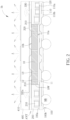
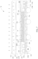
- FIG. 1 is a schematic, cross-sectional diagram showing an exemplary ultra-high frequency antenna package in accordance with an embodiment of the invention.
- the antenna package 1a comprises a redistribution layer (RDL) structure 100 having a top surface 100a and a bottom surface 100b opposite to the top surface 100a.
- the RDL structure 100 may include redistributed conductive layers 110 disposed in one or more dielectric layers 120.
- the redistributed conductive layers 110 may comprise connection patterns 110a at the top surface 100a and pad patterns 110b at the bottom surface 100b.
- solder balls SB may be disposed on the pad patterns 110b at the bottom surface 100b of the RDL structure 100.
- a TSV die 10 may be disposed on the top surface 100a of the RDL structure 100 and encapsulated by an insulating material such as epoxy molding compound 200.
- the TSV die 10 may be electrically connected to the RDL structure 100.
- the TSV die 10 comprises an active side 10a and a rear side 10b.
- the sidewall SW of the TSV die 10 is covered with the epoxy molding compound 200.
- the TSV die 10 may be a radio frequency (RF) chip, which may comprise a baseband processor or an application processor, but is not limited thereto.
- RF radio frequency
- the TSV die 10 may comprise a circuit region 11 on its active side 10a.
- integrated circuit devices such as transistors (not shown) are fabricated within the circuit region 11.
- the input/output (I/O) terminals in the circuit region 11 may be fanned out of the chip area and re-distributed through the RDL structure 100.
- the TSV die 10 may comprise a plurality of through-silicon-vias (TSVs) 12 and 13.
- TSVs through-silicon-vias
- the TSV 12 may be an RF signal via for transmitting ultra-high frequency signals
- the TSV 13 may be a ground via for transmitting ground signal.
- the plurality of TSVs 12 and 13 penetrate through an entire thickness of the TSV die 10 for connecting the circuit region 11 with an antenna structure ANT integrated on the rear side 10b of the TSV die 10.
- antenna package 1a Although only one integrated circuit die is illustrated in the antenna package 1a, it is understood that multiple integrated circuit dies (e.g., a separate baseband chip, processors, memory, etc.) may be integrated in a single semiconductor package in other embodiments depending on package design.
- integrated circuit dies e.g., a separate baseband chip, processors, memory, etc.
- the TSV die 10 transmits and receives wireless signals by way of one or more antennas elements of the antenna structure ANT integrated on the rear side 10b of the TSV die 10.
- the antenna structure ANT may be slot-coupling antenna structure comprising feed lines 310 connected to the TSV 12, a ground element layer 320 connected to the TSV 13, coupling slots 320s disposed in the ground element layer 320 and directly above the feed lines 310, and a dielectric layer 330.
- At least one passive element 210 may be disposed on the top surface 100a of the RDL structure 100 around the TSV die 10 and may be coupled to the connection patterns 110a at the top surface 100a of the RDL structure 100.
- the at least one passive element 210 and the TSV die 10 may be arranged on the RDL structure 100 in a side-by-side manner.
- the at least one passive element 210 may be a surface mount device, but is not limited thereto.
- the at least one passive element 210 may be a decoupling capacitor, an inductor, or a resistor.
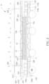
- FIG. 2 is a schematic, cross-sectional diagram showing an exemplary ultra-high frequency antenna package in accordance with another embodiment of the invention, wherein like regions, layers or elements are designated by like numeral numbers or labels.
- the antenna package 1b comprises an RDL structure 100 having a top surface 100a and a bottom surface 100b opposite to the top surface 100a.
- the RDL structure 100 may include redistributed conductive layers 110 disposed in one or more dielectric layers 120.
- the redistributed conductive layers 110 may comprise connection patterns 110a at the top surface 100a and pad patterns 110b at the bottom surface 100b.
- solder balls SB may be disposed on the pad patterns 110b at the bottom surface 100b of the RDL structure 100.
- a TSV die 10 may be disposed on the top surface 100a of the RDL structure 100 and encapsulated by an epoxy molding compound 200.
- the TSV die 10 may be electrically connected to the RDL structure 100.
- the TSV die 10 comprises an active side 10a and a rear side 10b.
- the sidewall SW of the TSV die 10 is covered with the epoxy molding compound 200.
- the TSV die 10 may be a radio frequency (RF) chip, which may comprise a baseband processor or an application processor, but is not limited thereto.
- RF radio frequency
- the TSV die 10 may comprise a circuit region 11 on its active side 10a.
- integrated circuit devices such as transistors (not shown) are fabricated within the circuit region 11.
- the I/O terminals in the circuit region 11 may be fanned out of the chip area and re-distributed through the RDL structure 100.
- the TSV die 10 may comprise a plurality of TSVs 12 and 13.
- the TSV 12 may be an RF signal via for transmitting ultra-high frequency signals and the TSV 13 may be a ground via for transmitting ground signal.
- the plurality of TSVs 12 and 13 penetrate through an entire thickness of the TSV die 10 for connecting the circuit region 11 with an antenna structure ANT integrated on the rear side 10b of the TSV die 10.
- the TSV die 10 transmits and receives wireless signals by way of one or more antennas elements of the antenna structure ANT integrated on the rear side 10b of the TSV die 10.
- the antenna structure ANT may be slot-coupled patch antenna structure comprising feed lines 310 connected to the TSV 12, a ground element layer 320 connected to the TSV 13, coupling slots 320s disposed in the ground element layer 320 and directly above the feed lines 310, a dielectric layer 330, a dielectric layer 400, and radiating elements 410 such as patch elements on the dielectric layer 400.
- the dielectric layer 400 may be an epoxy molding compound, but is not limited thereto.
- At least one passive element 210 may be disposed on the top surface 100a of the RDL structure 100 around the TSV die 10 and may be coupled to the connection patterns 110a at the top surface 100a of the RDL structure 100.
- the at least one passive element 210 and the TSV die 10 may be arranged on the RDL structure 100 in a side-by-side manner.
- the at least one passive element 210 may be a surface mount device, but is not limited thereto.
- the at least one passive element 210 may be a decoupling capacitor, an inductor, or a resistor.
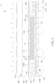
- FIG. 3 is a schematic, cross-sectional diagram showing an exemplary ultra-high frequency antenna package in accordance with another embodiment of the invention, wherein like regions, layers or elements are designated by like numeral numbers or labels.
- the difference between the antenna package 1b in FIG. 2 and the antenna package 1c in FIG. 3 is that the radiating elements 410 of the antenna package 1c are directly connected to the feed lines 310 through interconnect structures 420.
- the interconnect structures 420 may comprise copper pillars or through mold vias, but not limited thereto.
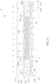
- FIG. 4 is a schematic, cross-sectional diagram showing an exemplary ultra-high frequency antenna package in accordance with another embodiment of the invention, wherein like regions, layers or elements are designated by like numeral numbers or labels.
- the difference between the antenna package 1c in FIG. 3 and the antenna package 1d in FIG. 4 is that the dielectric layer 400 of the antenna package 1d is a multi-layer structure, for example, a bi-layer structure.
- the dielectric layer 400 may comprise a lower dielectric layer 400a and an upper dielectric layer 400b.
- the lower dielectric layer 400a and the upper dielectric layer 400b may have different compositions.
- the lower dielectric layer 400a and the upper dielectric layer 400b may have different dielectric constants.
- the lower dielectric layer 400a may have a dielectric constant Dk lower than that of the upper dielectric layer 400b.
- the radiating elements 410 of the antenna package 1d are directly connected to the feed lines 310 through interconnect structures 420.
- the interconnect structures 420 may comprise conductive wires, traces, pillars or through mold vias, but not limited thereto.
- FIG. 5 is a schematic, cross-sectional diagram showing an exemplary ultra-high frequency antenna package in accordance with another embodiment of the invention, wherein like regions, layers or elements are designated by like numeral numbers or labels.
- the antenna package 1e comprises an RDL structure 100 having a top surface 100a and a bottom surface 100b opposite to the top surface 100a.
- the RDL structure 100 may include redistributed conductive layers 110 disposed in one or more dielectric layers 120.
- the redistributed conductive layers 110 may comprise connection patterns 110a at the top surface 100a and pad patterns 110b at the bottom surface 100b.
- solder balls SB may be disposed on the pad patterns 110b at the bottom surface 100b of the RDL structure 100.
- a TSV die 10 may be disposed on the top surface 100a of the RDL structure 100 and encapsulated by an epoxy molding compound 200.
- the TSV die 10 may be electrically connected to the RDL structure 100.
- the TSV die 10 comprises an active side 10a and a rear side 10b.
- the sidewall SW of the TSV die 10 is covered with the epoxy molding compound 200.
- the TSV die 10 may be an RF chip, which may comprise a baseband processor or an application processor, but is not limited thereto.
- the TSV die 10 may comprise a circuit region 11 on its active side 10a.
- integrated circuit devices such as transistors (not shown) are fabricated within the circuit region 11.
- the I/O terminals in the circuit region 11 may be fanned out of the chip area and re-distributed through the RDL structure 100.
- the TSV die 10 may comprise a plurality of TSVs 12 and 13.
- the TSV 12 may be an RF signal via for transmitting ultra-high frequency signals and the TSV 13 may be a ground via for transmitting ground signal.
- the plurality of TSVs 12 and 13 penetrate through an entire thickness of the TSV die 10 for connecting the circuit region 11 with an antenna structure ANT integrated on the rear side 10b of the TSV die 10.
- the TSV die 10 transmits and receives wireless signals by way of one or more antennas elements of the antenna structure ANT integrated on the rear side 10b of the TSV die 10.
- the antenna structure ANT may be slot-coupled, stacked patch antenna structure comprising feed lines 310 connected to the TSV 12, a ground element layer 320 connected to the TSV 13, coupling slots 320s disposed in the ground element layer 320 and directly above the feed lines 310, a dielectric layer 330, a dielectric layer 400 on the dielectric layer 330, patch elements 410 on the dielectric layer 400, a dielectric layer 500 on the dielectric layer 400, and patch elements 510 on the dielectric layer 500.
- the slot-coupled, stacked patch antenna structure can improve the bandwidth.
- FIG. 6 is a schematic, cross-sectional diagram showing an exemplary ultra-high frequency antenna package in accordance with another embodiment of the invention, wherein like regions, layers or elements are designated by like numeral numbers or labels.
- the antenna package 1f comprises an RDL structure 100 having a top surface 100a and a bottom surface 100b opposite to the top surface 100a.
- the RDL structure 100 may include redistributed conductive layers 110 disposed in one or more dielectric layers 120.
- the redistributed conductive layers 110 may comprise connection patterns 110a at the top surface 100a and pad patterns 110b at the bottom surface 100b.
- solder balls SB may be disposed on the pad patterns 110b at the bottom surface 100b of the RDL structure 100.
- a TSV die 10 may be disposed on the top surface 100a of the RDL structure 100 and encapsulated by an epoxy molding compound 200.
- the TSV die 10 may be electrically connected to the RDL structure 100.
- the TSV die 10 comprises an active side 10a and a rear side 10b.
- the sidewall SW of the TSV die 10 is covered with the epoxy molding compound 200.
- the TSV die 10 may be an RF chip, which may comprise a baseband processor or an application processor, but is not limited thereto.
- the TSV die 10 may comprise a circuit region 11 on its active side 10a.
- integrated circuit devices such as transistors (not shown) are fabricated within the circuit region 11.
- the I/O terminals in the circuit region 11 may be fanned out of the chip area and re-distributed through the RDL structure 100.
- the TSV die 10 may comprise a plurality of TSVs 12 and 13.
- the TSV 12 may be an RF signal via for transmitting ultra-high frequency signals and the TSV 13 may be a ground via for transmitting ground signal.
- the plurality of TSVs 12 and 13 penetrate through an entire thickness of the TSV die 10 for connecting the circuit region 11 with an antenna structure ANT integrated on the rear side 10b of the TSV die 10.
- the TSV die 10 transmits and receives wireless signals by way of one or more antennas elements of the antenna structure ANT integrated on the rear side 10b of the TSV die 10.
- the antenna structure ANT may be slot-coupled antenna structure comprising feed lines 310 connected to the TSV 12, a ground element layer 320 connected to the TSV 13, coupling slots 320s disposed in the ground element layer 320 and directly above the feed lines 310, a dielectric layer 330, a dielectric layer 600 on the dielectric layer 330, and a planar structure 610 on the dielectric layer 600.
- the planar structure 610 may comprise a frequency selective surface (FSS) structure.
- the planar structure 610 may comprise a metamaterial.
- FIG. 7 is a schematic, cross-sectional diagram showing an exemplary ultra-high frequency antenna package in accordance with another embodiment of the invention, wherein like regions, layers or elements are designated by like numeral numbers or labels.
- the antenna package 1g comprises an RDL structure 100 having a top surface 100a and a bottom surface 100b opposite to the top surface 100a.
- the RDL structure 100 may include redistributed conductive layers 110 disposed in one or more dielectric layers 120.
- the redistributed conductive layers 110 may comprise connection patterns 110a at the top surface 100a and pad patterns 110b at the bottom surface 100b.
- solder balls SB may be disposed on the pad patterns 110b at the bottom surface 100b of the RDL structure 100.
- a TSV die 10 may be disposed on the top surface 100a of the RDL structure 100 and encapsulated by an epoxy molding compound 200.
- the TSV die 10 may be electrically connected to the RDL structure 100.
- the TSV die 10 comprises an active side 10a and a rear side 10b.
- the sidewall SW of the TSV die 10 is covered with the epoxy molding compound 200.
- the TSV die 10 may be an RF chip, which may comprise a baseband processor or an application processor, but is not limited thereto.
- the TSV die 10 may comprise a circuit region 11 on its active side 10a.
- integrated circuit devices such as transistors (not shown) are fabricated within the circuit region 11.
- the I/O terminals in the circuit region 11 may be fanned out of the chip area and re-distributed through the RDL structure 100.
- the TSV die 10 may comprise a plurality of TSVs 12 and 13.
- the TSV 12 may be an RF signal via for transmitting ultra-high frequency signals and the TSV 13 may be a ground via for transmitting ground signal.
- the plurality of TSVs 12 and 13 penetrate through an entire thickness of the TSV die 10 for connecting the circuit region 11 with an antenna structure ANT integrated on the rear side 10b of the TSV die 10.
- the TSV die 10 transmits and receives wireless signals by way of one or more antennas elements of the antenna structure ANT integrated on the rear side 10b of the TSV die 10.
- the antenna structure ANT may be slot-coupled patch antenna structure comprising feed lines 310 connected to the TSV 12, a ground element layer 320 connected to the TSV 13, coupling slots 320s disposed in the ground element layer 320 and directly above the feed lines 310, a dielectric layer 330, a dielectric layer 400, radiating elements 410 such as patch elements on the dielectric layer 400, a dielectric layer 600 on the dielectric layer 400, and a planar structure 610 on the dielectric layer 600.
- the planar structure 610 may comprise a frequency selective surface (FSS) structure.
- the planar structure 610 may comprise a metamaterial.
- FIG. 8 is a schematic, cross-sectional diagram showing an exemplary ultra-high frequency antenna package in accordance with another embodiment of the invention, wherein like regions, layers or elements are designated by like numeral numbers or labels.
- the antenna package 1h comprises an RDL structure 100 having a top surface 100a and a bottom surface 100b opposite to the top surface 100a.
- the RDL structure 100 may include redistributed conductive layers 110 disposed in one or more dielectric layers 120.
- the redistributed conductive layers 110 may comprise connection patterns 110a at the top surface 100a and pad patterns 110b at the bottom surface 100b.
- solder balls SB such as C4 bumps may be disposed on the pad patterns 110b at the bottom surface 100b of the RDL structure 100.
- a TSV die 10 may be disposed on the top surface 100a of the RDL structure 100 and encapsulated by an epoxy molding compound 200.
- the TSV die 10 may be electrically connected to the RDL structure 100.
- the TSV die 10 comprises an active side 10a and a rear side 10b.
- the sidewall SW of the TSV die 10 is covered with the epoxy molding compound 200.
- the TSV die 10 may be an RF chip, which may comprise a baseband processor or an application processor, but is not limited thereto.
- the TSV die 10 may comprise a circuit region 11 on its active side 10a.
- integrated circuit devices such as transistors (not shown) are fabricated within the circuit region 11.
- the I/O terminals in the circuit region 11 may be fanned out of the chip area and re-distributed through the RDL structure 100.
- the TSV die 10 may comprise a plurality of TSVs 12 and 13.
- the TSV 12 may be an RF signal via for transmitting ultra-high frequency signals and the TSV 13 may be a ground via for transmitting ground signal.
- the plurality of TSVs 12 and 13 penetrate through an entire thickness of the TSV die 10 for connecting the circuit region 11 with an antenna structure ANT integrated on the rear side 10b of the TSV die 10.
- the TSV die 10 transmits and receives wireless signals by way of one or more antennas elements of the antenna structure ANT disposed on the rear side 10b of the TSV die 10.
- the antenna structure ANT may comprise feed lines 310 connected to the TSV 12, a ground element layer 320 connected to the TSV 13, coupling slots 320s disposed in the ground element layer 320 and directly above the feed lines 310, a dielectric layer 330, and an antenna substrate 700 mounted on the ground element layer 320.
- the antenna substrate 700 may comprise radiating elements 710 such as patch elements on the upper surface of the antenna substrate 700.
- the antenna substrate 700 may be electrically connected to the ground element layer 320 through a plurality of conductive elements 720 such as micro-bumps.
- the antenna substrate 700 may be a single-layer substrate or a multi-layer substrate and may comprise glass, ceramic or organic materials.
- FIG. 9 is a schematic, cross-sectional diagram showing an exemplary ultra-high frequency antenna package in accordance with another embodiment of the invention, wherein like regions, layers or elements are designated by like numeral numbers or labels.
- the antenna package 1i comprises an RDL structure 100 having a top surface 100a and a bottom surface 100b opposite to the top surface 100a.
- the RDL structure 100 may include redistributed conductive layers 110 disposed in one or more dielectric layers 120.
- the redistributed conductive layers 110 may comprise connection patterns 110a at the top surface 100a and pad patterns 110b at the bottom surface 100b.
- solder balls SB such as C4 bumps may be disposed on the pad patterns 110b at the bottom surface 100b of the RDL structure 100.
- a TSV die 10 may be disposed on the top surface 100a of the RDL structure 100 and encapsulated by an epoxy molding compound 200.
- the TSV die 10 may be electrically connected to the RDL structure 100.
- the TSV die 10 comprises an active side 10a and a rear side 10b.
- the sidewall SW of the TSV die 10 is covered with the epoxy molding compound 200.
- the TSV die 10 may be an RF chip, which may comprise a baseband processor or an application processor, but is not limited thereto.
- the TSV die 10 may comprise a circuit region 11 on its active side 10a.
- integrated circuit devices such as transistors (not shown) are fabricated within the circuit region 11.
- the I/O terminals in the circuit region 11 may be fanned out of the chip area and re-distributed through the RDL structure 100.
- the TSV die 10 may comprise a plurality of TSVs 12 and 13.
- the TSV 12 may be an RF signal via for transmitting ultra-high frequency signals and the TSV 13 may be a ground via for transmitting ground signal.
- the plurality of TSVs 12 and 13 penetrate through an entire thickness of the TSV die 10 for connecting the circuit region 11 with an antenna structure ANT integrated on the rear side 10b of the TSV die 10.
- the TSV die 10 transmits and receives wireless signals by way of one or more antennas elements of the antenna structure ANT disposed on the rear side 10b of the TSV die 10.
- the antenna structure ANT may comprise feed lines 310 connected to the TSV 12, a ground element layer 320 connected to the TSV 13, coupling slots 320s disposed in the ground element layer 320 and directly above the feed lines 310, a dielectric layer 330, multiple antenna substrates 700a, 700b mounted on the ground element layer 320.
- the antenna substrate 700a may comprise radiating elements 710a such as patch elements on the upper surface of the antenna substrate 700a.
- the antenna substrate 700b may comprise radiating elements 710b such as patch elements on the upper surface of the antenna substrate 700b.
- the antenna substrates 700a and 700b may be electrically connected to the ground element layer 320 through conductive elements 720a and 720b such as micro-bumps.
- the antenna substrates 700a, 700b may be a single-layer substrate or a multi-layer substrate and may comprise glass, ceramic or organic materials.
Landscapes
- Engineering & Computer Science (AREA)
- Microelectronics & Electronic Packaging (AREA)
- Waveguide Aerials (AREA)
- Internal Circuitry In Semiconductor Integrated Circuit Devices (AREA)
- Details Of Aerials (AREA)
- Semiconductor Integrated Circuits (AREA)
Abstract
Description
- This application claims the benefit of
U.S. Provisional Application No. 63/317,562, filed on March 8th, 2022 - The present disclosure relates generally to the field of semiconductor packaging. More particularly, the present disclosure relates to ultra-high frequency antenna packages with through-silicon-via (TSV) die.
- Next-generation communication systems and wearable technologies aim to achieve high data rates, low energy consumption, and massive connections because of the extensive increase in the number of Internet-of-Things (IoT) and wearable devices. These devices will be employed for many services such as cellular, environment monitoring, telemedicine, bio-medical, and smart traffic, etc. Therefore, it is challenging for the current communication devices to accommodate such a high number of services.
- Antenna in Package (AiP) or antenna on Package (AoP) has emerged as the mainstream antenna packaging technology for various millimeter-wave (mmWave) applications. AiP technology is an antenna packaging solution that implements an antenna or antennas in an IC package that can carry a bare RF chip. The AiP can be further integrated with front-end components (e.g., power amplifiers (PA) or low-noise amplifiers (LNA)), switches, filters and even power management integrated circuit (PMIC) to form an antenna module using System-in-Package (SiP) technologies.
- A typical AiP includes a RF chip attached to a package substrate with solder balls for connection to a main board. An array of antennas sits atop the upper portion of the package substrate, allowing wireless communication and detection. Flip-chip techniques are utilized to connect the RF chip to the substrate, thereby mitigating the interconnect loss. However, the routing loss of the antenna in a conventional AiP is high due to the routing design of the transmission line between the RF chip and the antenna.
- It is one object of the present disclosure to provide an improved antenna-in-package in order to solve the above-mentioned prior art deficiencies or shortcomings. An antenna package according to the invention is defined in the independent claims. The dependent claims define preferred embodiments thereof.
- One aspect of the present disclosure provides an antenna package including a redistribution layer (RDL) structure having a top surface and a bottom surface opposite to the top surface; a TSV die disposed on the top surface of the RDL structure, wherein the TSV die comprises an active side and a rear side, wherein the TSV die comprises a plurality of through-silicon-vias comprising RF signal vias and ground vias penetrating through an entire thickness of the TSV die; and an antenna structure disposed on the rear side of the TSV die and connecting to the RF signal vias and ground vias.
- Preferably, the RDL structure comprises redistributed conductive layers disposed in one or more dielectric layers.
- Preferably, the redistributed conductive layers comprise connection patterns at the top surface and pad patterns at the bottom surface, and wherein solder balls are disposed on the pad patterns at the bottom surface of the RDL structure.
- Preferably, the TSV die comprises a radio frequency (RF) chip.
- Preferably, the TSV die comprises a circuit region on its active side, and wherein input/output (I/O) terminals in the circuit region are fanned out of a chip area of the TSV die and re-distributed through the RDL structure.
- Preferably, the plurality of TSVs connects the circuit region with the antenna structure on the rear side of the TSV die.
- Preferably, the antenna structure comprises feed lines connected to the RF signal vias, a ground element layer connected to the ground vias, coupling slots disposed in the ground element layer and directly above the feed lines, and a first dielectric layer on the feed lines.
- Preferably, the antenna structure further comprises a second dielectric layer on the first dielectric layer, and first patch elements on the second dielectric layer.
- Preferably, the first patch elements are directly connected to the feed lines through interconnect structures.
- Preferably, the interconnect structures comprise copper pillars or through mold vias.
- Preferably, the second dielectric layer is a multi-layer structure.
- Preferably, the second dielectric layer comprises a lower dielectric layer and an upper dielectric layer.
- Preferably, the lower dielectric layer and the upper dielectric layer have different compositions.
- Preferably, the lower dielectric layer and the upper dielectric layer have different dielectric constants.
- Preferably, the lower dielectric layer has a dielectric constant that is lower than that of the upper dielectric layer.
- Preferably, the antenna structure comprises feed lines connected to the RF signal vias, a ground element layer connected to the ground vias, coupling slots disposed in the ground element layer and directly above the feed lines, a first dielectric layer, a second dielectric layer on the first dielectric layer, lower patch elements on the second dielectric layer, a third dielectric layer on the second dielectric layer, and upper patch elements on the third dielectric layer.
- Preferably, the antenna structure comprises feed lines connected to the RF signal vias, a ground element layer connected to the ground vias, coupling slots disposed in the ground element layer and directly above the feed lines, a first dielectric layer, a second dielectric layer on the first dielectric layer, and a planar structure on the second dielectric layer.
- Preferably, the planar structure comprises a frequency selective surface (FSS) structure.
- Preferably, the planar structure comprises a metamaterial.
- Preferably, the antenna structure comprises feed lines connected to the RF signal vias, a ground element layer connected to the ground vias, coupling slots disposed in the ground element layer and directly above the feed lines, a first dielectric layer, a second dielectric layer on the first dielectric layer, patch elements on the second dielectric layer, a third dielectric layer on the second dielectric layer, and a planar structure on the third dielectric layer.
- Preferably, the planar structure comprises a frequency selective surface (FSS) structure.
- Preferably, the planar structure comprises a metamaterial.
- Preferably, the antenna structure comprises feed lines connected to the RF signal vias, a ground element layer connected to the ground vias, coupling slots disposed in the ground element layer and directly above the feed lines, a first dielectric layer, and an antenna substrate mounted on the ground element layer.
- Preferably, the antenna substrate comprises patch elements on an upper surface of the antenna substrate.
- Preferably, the antenna substrate is electrically connected to the ground element layer through a plurality of conductive elements.
- Preferably, the antenna substrate comprises a single-layer substrate or a multi-layer substrate.
- Preferably, the antenna substrate comprises glass, ceramic or organic materials.
- Preferably, the antenna structure comprises feed lines connected to the RF signal vias, a ground element layer connected to the ground vias, coupling slots disposed in the ground element layer and directly above the feed lines, a first dielectric layer, and multiple antenna substrates mounted on the ground element layer.
- Preferably, at least one passive element is disposed on the top surface of the RDL structure around the TSV die and is coupled to the connection patterns at the top surface of the RDL structure.
- Preferably, the at least one passive element comprises a decoupling capacitor, an inductor, or a resistor.
- Preferably, the TSV die is encapsulated by an insulating material, and a sidewall of the TSV die is covered with the insulating material.
- Preferably, the insulating material comprises a molding compound.
- These and other objectives of the present invention will no doubt become obvious to those of ordinary skill in the art after reading the following detailed description of the preferred embodiment that is illustrated in the various figures and drawings.
- The accompanying drawings are included to provide a further understanding of the invention and are incorporated in and constitute a part of this specification. The drawings illustrate embodiments of the invention and, together with the description, serve to explain the principles of the invention. In the drawings:
-
FIG. 1 is a schematic, cross-sectional diagram showing an exemplary ultra-high frequency antenna package in accordance with an embodiment of the invention; -
FIG. 2 is a schematic, cross-sectional diagram showing an exemplary ultra-high frequency antenna package in accordance with another embodiment of the invention; -
FIG. 3 is a schematic, cross-sectional diagram showing an exemplary ultra-high frequency antenna package in accordance with another embodiment of the invention; -
FIG. 4 is a schematic, cross-sectional diagram showing an exemplary ultra-high frequency antenna package in accordance with another embodiment of the invention; -
FIG. 5 is a schematic, cross-sectional diagram showing an exemplary ultra-high frequency antenna package in accordance with another embodiment of the invention; -
FIG. 6 is a schematic, cross-sectional diagram showing an exemplary ultra-high frequency antenna package in accordance with another embodiment of the invention; -
FIG. 7 is a schematic, cross-sectional diagram showing an exemplary ultra-high frequency antenna package in accordance with another embodiment of the invention; -
FIG. 8 is a schematic, cross-sectional diagram showing an exemplary ultra-high frequency antenna package in accordance with another embodiment of the invention; and -
FIG. 9 is a schematic, cross-sectional diagram showing an exemplary ultra-high frequency antenna package in accordance with another embodiment of the invention. - In the following detailed description of embodiments of the invention, reference is made to the accompanying drawings, which form a part hereof, and in which is shown by way of illustration specific preferred embodiments in which the disclosure may be practiced.
- These embodiments are described in sufficient detail to enable those skilled in the art to practice them, and it is to be understood that other embodiments may be utilized and that mechanical, chemical, electrical, and procedural changes may be made without departing from the scope of the present disclosure. The following detailed description is, therefore, not to be taken in a limiting sense, and the scope of embodiments of the present invention is defined only by the appended claims.
- It will be understood that when an element or layer is referred to as being "on", "connected to" or "coupled to" another element or layer, it can be directly on, connected or coupled to the other element or layer or intervening elements or layers may be present. In contrast, when an element is referred to as being "directly on," "directly connected to" or "directly coupled to" another element or layer, there are no intervening elements or layers present. Like numbers refer to like elements throughout. As used herein, the term "and/or" includes any and all combinations of one or more of the associated listed items.
- THz frequency bands from 100 to 300 GHz are considered for 6G communication. The complexity of antenna and chip package design increases at such higher frequencies, which in return creates more challenges in terms of material selection, design process, fabrication techniques, and experimental validations. The present disclosure provides various antenna packages with through-silicon-via (TSV) die for reducing routing loss, which are suited for future 6G applications.
-
FIG. 1 is a schematic, cross-sectional diagram showing an exemplary ultra-high frequency antenna package in accordance with an embodiment of the invention. As shown inFIG. 1 , the antenna package 1a comprises a redistribution layer (RDL)structure 100 having atop surface 100a and abottom surface 100b opposite to thetop surface 100a. Preferably, theRDL structure 100 may include redistributedconductive layers 110 disposed in one or moredielectric layers 120. Preferably, the redistributedconductive layers 110 may compriseconnection patterns 110a at thetop surface 100a andpad patterns 110b at thebottom surface 100b. Preferably, solder balls SB may be disposed on thepad patterns 110b at thebottom surface 100b of theRDL structure 100. - Preferably, a TSV die 10 may be disposed on the
top surface 100a of theRDL structure 100 and encapsulated by an insulating material such asepoxy molding compound 200. Preferably, the TSV die 10 may be electrically connected to theRDL structure 100. The TSV die 10 comprises anactive side 10a and arear side 10b. The sidewall SW of the TSV die 10 is covered with theepoxy molding compound 200. Preferably, the TSV die 10 may be a radio frequency (RF) chip, which may comprise a baseband processor or an application processor, but is not limited thereto. - Preferably, the TSV die 10 may comprise a
circuit region 11 on itsactive side 10a. Preferably, integrated circuit devices such as transistors (not shown) are fabricated within thecircuit region 11. The input/output (I/O) terminals in thecircuit region 11 may be fanned out of the chip area and re-distributed through theRDL structure 100. - Preferably, the TSV die 10 may comprise a plurality of through-silicon-vias (TSVs) 12 and 13. Preferably, the
TSV 12 may be an RF signal via for transmitting ultra-high frequency signals and theTSV 13 may be a ground via for transmitting ground signal. The plurality ofTSVs circuit region 11 with an antenna structure ANT integrated on therear side 10b of the TSV die 10. - Although only one integrated circuit die is illustrated in the antenna package 1a, it is understood that multiple integrated circuit dies (e.g., a separate baseband chip, processors, memory, etc.) may be integrated in a single semiconductor package in other embodiments depending on package design.
- Preferably, the TSV die 10 transmits and receives wireless signals by way of one or more antennas elements of the antenna structure ANT integrated on the
rear side 10b of the TSV die 10. For example, the antenna structure ANT may be slot-coupling antenna structure comprisingfeed lines 310 connected to theTSV 12, aground element layer 320 connected to theTSV 13,coupling slots 320s disposed in theground element layer 320 and directly above thefeed lines 310, and adielectric layer 330. - Preferably, optionally, at least one
passive element 210 may be disposed on thetop surface 100a of theRDL structure 100 around the TSV die 10 and may be coupled to theconnection patterns 110a at thetop surface 100a of theRDL structure 100. Preferably, the at least onepassive element 210 and the TSV die 10 may be arranged on theRDL structure 100 in a side-by-side manner. Preferably, the at least onepassive element 210 may be a surface mount device, but is not limited thereto. Preferably, for example, the at least onepassive element 210 may be a decoupling capacitor, an inductor, or a resistor. -
FIG. 2 is a schematic, cross-sectional diagram showing an exemplary ultra-high frequency antenna package in accordance with another embodiment of the invention, wherein like regions, layers or elements are designated by like numeral numbers or labels. As shown inFIG. 2 , likewise, the antenna package 1b comprises anRDL structure 100 having atop surface 100a and abottom surface 100b opposite to thetop surface 100a. Preferably, theRDL structure 100 may include redistributedconductive layers 110 disposed in one or moredielectric layers 120. Preferably, the redistributedconductive layers 110 may compriseconnection patterns 110a at thetop surface 100a andpad patterns 110b at thebottom surface 100b. Preferably, solder balls SB may be disposed on thepad patterns 110b at thebottom surface 100b of theRDL structure 100. - Preferably, a TSV die 10 may be disposed on the
top surface 100a of theRDL structure 100 and encapsulated by anepoxy molding compound 200. Preferably, the TSV die 10 may be electrically connected to theRDL structure 100. The TSV die 10 comprises anactive side 10a and arear side 10b. The sidewall SW of the TSV die 10 is covered with theepoxy molding compound 200. Preferably, the TSV die 10 may be a radio frequency (RF) chip, which may comprise a baseband processor or an application processor, but is not limited thereto. - Preferably, the TSV die 10 may comprise a
circuit region 11 on itsactive side 10a. Preferably, integrated circuit devices such as transistors (not shown) are fabricated within thecircuit region 11. The I/O terminals in thecircuit region 11 may be fanned out of the chip area and re-distributed through theRDL structure 100. - Preferably, likewise, the TSV die 10 may comprise a plurality of
TSVs TSV 12 may be an RF signal via for transmitting ultra-high frequency signals and theTSV 13 may be a ground via for transmitting ground signal. The plurality ofTSVs circuit region 11 with an antenna structure ANT integrated on therear side 10b of the TSV die 10. - Preferably, the TSV die 10 transmits and receives wireless signals by way of one or more antennas elements of the antenna structure ANT integrated on the
rear side 10b of the TSV die 10. For example, the antenna structure ANT may be slot-coupled patch antenna structure comprisingfeed lines 310 connected to theTSV 12, aground element layer 320 connected to theTSV 13,coupling slots 320s disposed in theground element layer 320 and directly above thefeed lines 310, adielectric layer 330, adielectric layer 400, and radiatingelements 410 such as patch elements on thedielectric layer 400. Preferably, thedielectric layer 400 may be an epoxy molding compound, but is not limited thereto. - Preferably, optionally, at least one
passive element 210 may be disposed on thetop surface 100a of theRDL structure 100 around the TSV die 10 and may be coupled to theconnection patterns 110a at thetop surface 100a of theRDL structure 100. Preferably, the at least onepassive element 210 and the TSV die 10 may be arranged on theRDL structure 100 in a side-by-side manner. Preferably, the at least onepassive element 210 may be a surface mount device, but is not limited thereto. Preferably, for example, the at least onepassive element 210 may be a decoupling capacitor, an inductor, or a resistor. -
FIG. 3 is a schematic, cross-sectional diagram showing an exemplary ultra-high frequency antenna package in accordance with another embodiment of the invention, wherein like regions, layers or elements are designated by like numeral numbers or labels. As shown inFIG. 3 , the difference between the antenna package 1b inFIG. 2 and the antenna package 1c inFIG. 3 is that the radiatingelements 410 of the antenna package 1c are directly connected to thefeed lines 310 throughinterconnect structures 420. Preferably, for example, theinterconnect structures 420 may comprise copper pillars or through mold vias, but not limited thereto. -
FIG. 4 is a schematic, cross-sectional diagram showing an exemplary ultra-high frequency antenna package in accordance with another embodiment of the invention, wherein like regions, layers or elements are designated by like numeral numbers or labels. As shown inFIG. 4 , the difference between the antenna package 1c inFIG. 3 and the antenna package 1d inFIG. 4 is that thedielectric layer 400 of the antenna package 1d is a multi-layer structure, for example, a bi-layer structure. Preferably, for example, thedielectric layer 400 may comprise alower dielectric layer 400a and anupper dielectric layer 400b. Preferably, for example, thelower dielectric layer 400a and theupper dielectric layer 400b may have different compositions. Preferably, for example, thelower dielectric layer 400a and theupper dielectric layer 400b may have different dielectric constants. Preferably, for example, thelower dielectric layer 400a may have a dielectric constant Dk lower than that of theupper dielectric layer 400b. InFIG. 4 , the radiatingelements 410 of the antenna package 1d are directly connected to thefeed lines 310 throughinterconnect structures 420. Preferably, for example, theinterconnect structures 420 may comprise conductive wires, traces, pillars or through mold vias, but not limited thereto. -
FIG. 5 is a schematic, cross-sectional diagram showing an exemplary ultra-high frequency antenna package in accordance with another embodiment of the invention, wherein like regions, layers or elements are designated by like numeral numbers or labels. As shown inFIG. 5 , likewise, the antenna package 1e comprises anRDL structure 100 having atop surface 100a and abottom surface 100b opposite to thetop surface 100a. Preferably, theRDL structure 100 may include redistributedconductive layers 110 disposed in one or moredielectric layers 120. Preferably, the redistributedconductive layers 110 may compriseconnection patterns 110a at thetop surface 100a andpad patterns 110b at thebottom surface 100b. Preferably, solder balls SB may be disposed on thepad patterns 110b at thebottom surface 100b of theRDL structure 100. - Preferably, a TSV die 10 may be disposed on the
top surface 100a of theRDL structure 100 and encapsulated by anepoxy molding compound 200. Preferably, the TSV die 10 may be electrically connected to theRDL structure 100. The TSV die 10 comprises anactive side 10a and arear side 10b. The sidewall SW of the TSV die 10 is covered with theepoxy molding compound 200. Preferably, the TSV die 10 may be an RF chip, which may comprise a baseband processor or an application processor, but is not limited thereto. - Preferably, the TSV die 10 may comprise a
circuit region 11 on itsactive side 10a. Preferably, integrated circuit devices such as transistors (not shown) are fabricated within thecircuit region 11. The I/O terminals in thecircuit region 11 may be fanned out of the chip area and re-distributed through theRDL structure 100. - Preferably, likewise, the TSV die 10 may comprise a plurality of
TSVs TSV 12 may be an RF signal via for transmitting ultra-high frequency signals and theTSV 13 may be a ground via for transmitting ground signal. The plurality ofTSVs circuit region 11 with an antenna structure ANT integrated on therear side 10b of the TSV die 10. - Preferably, the TSV die 10 transmits and receives wireless signals by way of one or more antennas elements of the antenna structure ANT integrated on the
rear side 10b of the TSV die 10. For example, the antenna structure ANT may be slot-coupled, stacked patch antenna structure comprisingfeed lines 310 connected to theTSV 12, aground element layer 320 connected to theTSV 13,coupling slots 320s disposed in theground element layer 320 and directly above thefeed lines 310, adielectric layer 330, adielectric layer 400 on thedielectric layer 330,patch elements 410 on thedielectric layer 400, adielectric layer 500 on thedielectric layer 400, and patchelements 510 on thedielectric layer 500. The slot-coupled, stacked patch antenna structure can improve the bandwidth. -
FIG. 6 is a schematic, cross-sectional diagram showing an exemplary ultra-high frequency antenna package in accordance with another embodiment of the invention, wherein like regions, layers or elements are designated by like numeral numbers or labels. As shown inFIG. 6 , likewise, the antenna package 1f comprises anRDL structure 100 having atop surface 100a and abottom surface 100b opposite to thetop surface 100a. Preferably, theRDL structure 100 may include redistributedconductive layers 110 disposed in one or moredielectric layers 120. Preferably, the redistributedconductive layers 110 may compriseconnection patterns 110a at thetop surface 100a andpad patterns 110b at thebottom surface 100b. Preferably, solder balls SB may be disposed on thepad patterns 110b at thebottom surface 100b of theRDL structure 100. - Preferably, a TSV die 10 may be disposed on the
top surface 100a of theRDL structure 100 and encapsulated by anepoxy molding compound 200. Preferably, the TSV die 10 may be electrically connected to theRDL structure 100. The TSV die 10 comprises anactive side 10a and arear side 10b. The sidewall SW of the TSV die 10 is covered with theepoxy molding compound 200. Preferably, the TSV die 10 may be an RF chip, which may comprise a baseband processor or an application processor, but is not limited thereto. - Preferably, the TSV die 10 may comprise a
circuit region 11 on itsactive side 10a. Preferably, integrated circuit devices such as transistors (not shown) are fabricated within thecircuit region 11. The I/O terminals in thecircuit region 11 may be fanned out of the chip area and re-distributed through theRDL structure 100. - Preferably, likewise, the TSV die 10 may comprise a plurality of
TSVs TSV 12 may be an RF signal via for transmitting ultra-high frequency signals and theTSV 13 may be a ground via for transmitting ground signal. The plurality ofTSVs circuit region 11 with an antenna structure ANT integrated on therear side 10b of the TSV die 10. - Preferably, the TSV die 10 transmits and receives wireless signals by way of one or more antennas elements of the antenna structure ANT integrated on the
rear side 10b of the TSV die 10. For example, the antenna structure ANT may be slot-coupled antenna structure comprisingfeed lines 310 connected to theTSV 12, aground element layer 320 connected to theTSV 13,coupling slots 320s disposed in theground element layer 320 and directly above thefeed lines 310, adielectric layer 330, adielectric layer 600 on thedielectric layer 330, and aplanar structure 610 on thedielectric layer 600. Preferably, for example, theplanar structure 610 may comprise a frequency selective surface (FSS) structure. Preferably, for example, theplanar structure 610 may comprise a metamaterial. -
FIG. 7 is a schematic, cross-sectional diagram showing an exemplary ultra-high frequency antenna package in accordance with another embodiment of the invention, wherein like regions, layers or elements are designated by like numeral numbers or labels. As shown inFIG. 7 , likewise, the antenna package 1g comprises anRDL structure 100 having atop surface 100a and abottom surface 100b opposite to thetop surface 100a. Preferably, theRDL structure 100 may include redistributedconductive layers 110 disposed in one or moredielectric layers 120. Preferably, the redistributedconductive layers 110 may compriseconnection patterns 110a at thetop surface 100a andpad patterns 110b at thebottom surface 100b. Preferably, solder balls SB may be disposed on thepad patterns 110b at thebottom surface 100b of theRDL structure 100. - Preferably, a TSV die 10 may be disposed on the
top surface 100a of theRDL structure 100 and encapsulated by anepoxy molding compound 200. Preferably, the TSV die 10 may be electrically connected to theRDL structure 100. The TSV die 10 comprises anactive side 10a and arear side 10b. The sidewall SW of the TSV die 10 is covered with theepoxy molding compound 200. Preferably, the TSV die 10 may be an RF chip, which may comprise a baseband processor or an application processor, but is not limited thereto. - Preferably, the TSV die 10 may comprise a
circuit region 11 on itsactive side 10a. Preferably, integrated circuit devices such as transistors (not shown) are fabricated within thecircuit region 11. The I/O terminals in thecircuit region 11 may be fanned out of the chip area and re-distributed through theRDL structure 100. - Preferably, likewise, the TSV die 10 may comprise a plurality of
TSVs TSV 12 may be an RF signal via for transmitting ultra-high frequency signals and theTSV 13 may be a ground via for transmitting ground signal. The plurality ofTSVs circuit region 11 with an antenna structure ANT integrated on therear side 10b of the TSV die 10. - Preferably, the TSV die 10 transmits and receives wireless signals by way of one or more antennas elements of the antenna structure ANT integrated on the
rear side 10b of the TSV die 10. For example, the antenna structure ANT may be slot-coupled patch antenna structure comprisingfeed lines 310 connected to theTSV 12, aground element layer 320 connected to theTSV 13,coupling slots 320s disposed in theground element layer 320 and directly above thefeed lines 310, adielectric layer 330, adielectric layer 400, radiatingelements 410 such as patch elements on thedielectric layer 400, adielectric layer 600 on thedielectric layer 400, and aplanar structure 610 on thedielectric layer 600. Preferably, for example, theplanar structure 610 may comprise a frequency selective surface (FSS) structure. Preferably, for example, theplanar structure 610 may comprise a metamaterial. -
FIG. 8 is a schematic, cross-sectional diagram showing an exemplary ultra-high frequency antenna package in accordance with another embodiment of the invention, wherein like regions, layers or elements are designated by like numeral numbers or labels. As shown inFIG. 8 , likewise, the antenna package 1h comprises anRDL structure 100 having atop surface 100a and abottom surface 100b opposite to thetop surface 100a. Preferably, theRDL structure 100 may include redistributedconductive layers 110 disposed in one or moredielectric layers 120. Preferably, the redistributedconductive layers 110 may compriseconnection patterns 110a at thetop surface 100a andpad patterns 110b at thebottom surface 100b. Preferably, solder balls SB such as C4 bumps may be disposed on thepad patterns 110b at thebottom surface 100b of theRDL structure 100. - Preferably, a TSV die 10 may be disposed on the
top surface 100a of theRDL structure 100 and encapsulated by anepoxy molding compound 200. Preferably, the TSV die 10 may be electrically connected to theRDL structure 100. The TSV die 10 comprises anactive side 10a and arear side 10b. The sidewall SW of the TSV die 10 is covered with theepoxy molding compound 200. Preferably, the TSV die 10 may be an RF chip, which may comprise a baseband processor or an application processor, but is not limited thereto. - Preferably, the TSV die 10 may comprise a
circuit region 11 on itsactive side 10a. Preferably, integrated circuit devices such as transistors (not shown) are fabricated within thecircuit region 11. The I/O terminals in thecircuit region 11 may be fanned out of the chip area and re-distributed through theRDL structure 100. - Preferably, likewise, the TSV die 10 may comprise a plurality of
TSVs TSV 12 may be an RF signal via for transmitting ultra-high frequency signals and theTSV 13 may be a ground via for transmitting ground signal. The plurality ofTSVs circuit region 11 with an antenna structure ANT integrated on therear side 10b of the TSV die 10. - Preferably, the TSV die 10 transmits and receives wireless signals by way of one or more antennas elements of the antenna structure ANT disposed on the
rear side 10b of the TSV die 10. For example, the antenna structure ANT may comprisefeed lines 310 connected to theTSV 12, aground element layer 320 connected to theTSV 13,coupling slots 320s disposed in theground element layer 320 and directly above thefeed lines 310, adielectric layer 330, and anantenna substrate 700 mounted on theground element layer 320. Preferably, theantenna substrate 700 may comprise radiatingelements 710 such as patch elements on the upper surface of theantenna substrate 700. Preferably, theantenna substrate 700 may be electrically connected to theground element layer 320 through a plurality ofconductive elements 720 such as micro-bumps. Preferably, theantenna substrate 700 may be a single-layer substrate or a multi-layer substrate and may comprise glass, ceramic or organic materials. -
FIG. 9 is a schematic, cross-sectional diagram showing an exemplary ultra-high frequency antenna package in accordance with another embodiment of the invention, wherein like regions, layers or elements are designated by like numeral numbers or labels. As shown inFIG. 9 , likewise, the antenna package 1i comprises anRDL structure 100 having atop surface 100a and abottom surface 100b opposite to thetop surface 100a. Preferably, theRDL structure 100 may include redistributedconductive layers 110 disposed in one or moredielectric layers 120. Preferably, the redistributedconductive layers 110 may compriseconnection patterns 110a at thetop surface 100a andpad patterns 110b at thebottom surface 100b. Preferably, solder balls SB such as C4 bumps may be disposed on thepad patterns 110b at thebottom surface 100b of theRDL structure 100. - Preferably, a TSV die 10 may be disposed on the
top surface 100a of theRDL structure 100 and encapsulated by anepoxy molding compound 200. Preferably, the TSV die 10 may be electrically connected to theRDL structure 100. The TSV die 10 comprises anactive side 10a and arear side 10b. The sidewall SW of the TSV die 10 is covered with theepoxy molding compound 200. Preferably, the TSV die 10 may be an RF chip, which may comprise a baseband processor or an application processor, but is not limited thereto. - Preferably, the TSV die 10 may comprise a
circuit region 11 on itsactive side 10a. Preferably, integrated circuit devices such as transistors (not shown) are fabricated within thecircuit region 11. The I/O terminals in thecircuit region 11 may be fanned out of the chip area and re-distributed through theRDL structure 100. - Preferably, likewise, the TSV die 10 may comprise a plurality of
TSVs TSV 12 may be an RF signal via for transmitting ultra-high frequency signals and theTSV 13 may be a ground via for transmitting ground signal. The plurality ofTSVs circuit region 11 with an antenna structure ANT integrated on therear side 10b of the TSV die 10. - Preferably, the TSV die 10 transmits and receives wireless signals by way of one or more antennas elements of the antenna structure ANT disposed on the
rear side 10b of the TSV die 10. For example, the antenna structure ANT may comprisefeed lines 310 connected to theTSV 12, aground element layer 320 connected to theTSV 13,coupling slots 320s disposed in theground element layer 320 and directly above thefeed lines 310, adielectric layer 330,multiple antenna substrates ground element layer 320. Preferably, theantenna substrate 700a may comprise radiatingelements 710a such as patch elements on the upper surface of theantenna substrate 700a. Preferably, theantenna substrate 700b may comprise radiatingelements 710b such as patch elements on the upper surface of theantenna substrate 700b. Preferably, theantenna substrates ground element layer 320 throughconductive elements antenna substrates - Those skilled in the art will readily observe that numerous modifications and alterations of the device and method may be made while retaining the teachings of the invention. Accordingly, the above disclosure should be construed as limited only by the metes and bounds of the appended claims.
Claims (15)
- An antenna package, comprising:a redistribution layer, in the following also referred to as RDL, structure (100) having a top surface (100a) and a bottom surface (100b) opposite to the top surface (100a);a TSV die (10) disposed on the top surface (100a) of the RDL structure (100), wherein the TSV die (10) comprises an active side (10a) and a rear side (10b), wherein the TSV die (10) comprises a plurality of through-silicon-vias (12, 13) comprising RF signal vias (12) and ground vias (13) penetrating through an entire thickness of the TSV die (10); andan antenna structure (ANT) disposed on the rear side (10b) of the TSV die (10) and connecting to the RF signal vias (12) and ground vias (13).
- The antenna package according to claim 1, wherein the RDL structure (100) comprises redistributed conductive layers (110) disposed in one or more dielectric layers (120).
- The antenna package according to claim 2, wherein the redistributed conductive layers (110) comprise connection patterns (110a) at the top surface (100a) and pad patterns (110b) at the bottom surface (100b), and wherein solder balls (SB) are disposed on the pad patterns (110b) at the bottom surface (100b) of the RDL structure (100).
- The antenna package according to any one of claims 1 to 3, wherein the TSV die (10) comprises a radio frequency, in the following also referred to as RF, chip; and/orwherein the TSV die (10) comprises a circuit region (11) on its active side (10a), and wherein input/output, in the following also referred to as I/O, terminals in the circuit region (11) are fanned out of a chip area of the TSV die (10) and re-distributed through the RDL structure (100),wherein preferably the plurality of through-silicon-vias (12, 13) connects the circuit region (11) with the antenna structure (ANT) on the rear side (10b) of the TSV die (10).
- The antenna package according to any one of claims 1 to 4, wherein the antenna structure (ANT) comprises feed lines (310) connected to the RF signal vias (12), a ground element layer (320) connected to the ground vias (13), coupling slots (320s) disposed in the ground element layer (320) and directly above the feed lines (310), and a first dielectric layer (330) on the feed lines (310).
- The antenna package according to claim 5, wherein the antenna structure (ANT) further comprises a second dielectric layer (400) on the first dielectric layer (330), and first patch elements (410) on the second dielectric layer (400).
- The antenna package according to claim 6, wherein the first patch elements (410) are directly connected to the feed lines (310) through interconnect structures (420),wherein preferably the interconnect structures (420) comprise copper pillars or through mold vias; and/orwherein the second dielectric layer (400) is a multi-layer structure,wherein preferably the second dielectric layer (400) comprises a lower dielectric layer (400a) and an upper dielectric layer (400b),wherein further preferably the lower dielectric layer (400a) and the upper dielectric layer (400b) have different compositions and/or different dielectric constants, and/orwherein further preferably the lower dielectric layer (400a) has a dielectric constant that is lower than that of the upper dielectric layer (400b).
- The antenna package according to any one of claims 1 to 7, wherein the antenna structure (ANT) comprises feed lines (310) connected to the RF signal vias (12), a ground element layer (320) connected to the ground vias (13), coupling slots (320s) disposed in the ground element layer (320) and directly above the feed lines (310), a first dielectric layer (330), a second dielectric layer (400) on the first dielectric layer (330), lower patch elements (410) on the second dielectric layer (400), a third dielectric layer (500) on the second dielectric layer (400), and upper patch elements (510) on the third dielectric layer (500).
- The antenna package according to any one of claims 1 to 8, wherein the antenna structure (ANT) comprises feed lines (310) connected to the RF signal vias (12), a ground element layer (320) connected to the ground vias (13), coupling slots (320s) disposed in the ground element layer (320) and directly above the feed lines (310), a first dielectric layer (330), a second dielectric layer (600; 400) on the first dielectric layer (330), anda) a planar structure (610) on the second dielectric layer (600), orb) patch elements (410) on the second dielectric layer (400), a third dielectric layer (600) on the second dielectric layer (400), and a planar structure (610) on the third dielectric layer (600).
- The antenna package according to claim 9, wherein the planar structure (610) comprises a frequency selective surface, in the following also referred to as FSS, structure; and/or
wherein the planar structure (610) comprises a metamaterial. - The antenna package according to any one of claims 1 to 10, wherein the antenna structure (ANT) comprises feed lines (310) connected to the RF signal vias (12), a ground element layer (320) connected to the ground vias (13), coupling slots (320s) disposed in the ground element layer (320) and directly above the feed lines (310), a first dielectric layer (330), and an antenna substrate (700) mounted on the ground element layer (320).
- The antenna package according to claim 11, wherein the antenna substrate (700) comprises patch elements (710) on an upper surface of the antenna substrate (700); and/orwherein the antenna substrate (700) is electrically connected to the ground element layer (320) through a plurality of conductive elements (720); and/orwherein the antenna substrate (700) comprises a single-layer substrate or a multi-layer substrate; and/orwherein the antenna substrate (700) comprises glass, ceramic or organic materials.
- The antenna package according to any one of claims 1 to 12, wherein the antenna structure (ANT) comprises feed lines (310) connected to the RF signal vias (12), a ground element layer (320) connected to the ground vias (13), coupling slots (320s) disposed in the ground element layer (320) and directly above the feed lines (310), a first dielectric layer (330), and multiple antenna substrates (700a, 700b) mounted on the ground element layer (320).
- The antenna package according to any one of claims 1 to 13, wherein at least one passive element (210) is disposed on the top surface (100a) of the RDL structure (100) around the TSV die (10) and is coupled to the connection patterns (110a) at the top surface (100a) of the RDL structure (100);
wherein preferably the at least one passive element (210) comprises a decoupling capacitor, an inductor, or a resistor. - The antenna package according to any one of claims 1 to 14, wherein the TSV die (10) is encapsulated by an insulating material (200), and a sidewall (SW) of the TSV die (10) is covered with the insulating material (200);
wherein preferably the insulating material (200) comprises a molding compound.
Applications Claiming Priority (2)
| Application Number | Priority Date | Filing Date | Title |
|---|---|---|---|
| US202263317562P | 2022-03-08 | 2022-03-08 | |
| US18/109,266 US20230290700A1 (en) | 2022-03-08 | 2023-02-14 | Antenna package |
Publications (2)
| Publication Number | Publication Date |
|---|---|
| EP4243068A2 true EP4243068A2 (en) | 2023-09-13 |
| EP4243068A3 EP4243068A3 (en) | 2023-10-04 |
Family
ID=85462470
Family Applications (1)
| Application Number | Title | Priority Date | Filing Date |
|---|---|---|---|
| EP23159948.1A Pending EP4243068A3 (en) | 2022-03-08 | 2023-03-03 | Antenna package |
Country Status (3)
| Country | Link |
|---|---|
| US (1) | US20230290700A1 (en) |
| EP (1) | EP4243068A3 (en) |
| TW (1) | TWI841266B (en) |
Families Citing this family (2)
| Publication number | Priority date | Publication date | Assignee | Title |
|---|---|---|---|---|
| US12512593B2 (en) * | 2023-04-13 | 2025-12-30 | Qualcomm Incorporated | Antenna module as a radio-frequency (RF) integrated circuit (IC) die with an integrated antenna substrate, and related fabrication methods |
| US20250167154A1 (en) * | 2023-11-20 | 2025-05-22 | Rockwell Collins, Inc. | Advanced high frequency aesa antenna connection method |
Family Cites Families (12)
| Publication number | Priority date | Publication date | Assignee | Title |
|---|---|---|---|---|
| US8786060B2 (en) * | 2012-05-04 | 2014-07-22 | Advanced Semiconductor Engineering, Inc. | Semiconductor package integrated with conformal shield and antenna |
| US10403511B2 (en) * | 2013-01-14 | 2019-09-03 | Intel Corporation | Backside redistribution layer patch antenna |
| CN106716636B (en) * | 2014-09-17 | 2021-05-28 | 英特尔公司 | Die with integrated microphone device using through silicon vias (TSVs) |
| US9576918B2 (en) * | 2015-05-20 | 2017-02-21 | Intel IP Corporation | Conductive paths through dielectric with a high aspect ratio for semiconductor devices |
| WO2017052658A1 (en) * | 2015-09-25 | 2017-03-30 | Intel Corporation | Integrated stacked strata of functional die islands in a semiconductor device |
| CN112349702B (en) * | 2019-08-07 | 2024-12-20 | 联发科技股份有限公司 | Semiconductor packaging |
| US11329017B2 (en) * | 2020-04-29 | 2022-05-10 | Advanced Semiconductor Engineering, Inc. | Semiconductor device package and method of manufacturing the same |
| US11756894B2 (en) * | 2020-05-20 | 2023-09-12 | Qualcomm Incorporated | Radio-frequency (RF) integrated circuit (IC) (RFIC) packages employing a substrate sidewall partial shield for electro-magnetic interference (EMI) shielding, and related fabrication methods |
| KR102766659B1 (en) * | 2020-05-20 | 2025-02-12 | 에스케이하이닉스 주식회사 | Stack package including core die stacked over controlling die |
| US11456291B2 (en) * | 2020-06-24 | 2022-09-27 | Qualcomm Incorporated | Integrated circuit (IC) packages employing split, double-sided metallization structures to facilitate a semiconductor die (“die”) module employing stacked dice, and related fabrication methods |
| US11870130B2 (en) * | 2020-07-27 | 2024-01-09 | Infineon Technologies Ag | Antenna apparatus and fabrication method |
| KR102853924B1 (en) * | 2020-08-03 | 2025-09-01 | 삼성전자주식회사 | Semiconductor package |
-
2023
- 2023-02-14 US US18/109,266 patent/US20230290700A1/en active Pending
- 2023-03-02 TW TW112107467A patent/TWI841266B/en active
- 2023-03-03 EP EP23159948.1A patent/EP4243068A3/en active Pending
Also Published As
| Publication number | Publication date |
|---|---|
| TWI841266B (en) | 2024-05-01 |
| EP4243068A3 (en) | 2023-10-04 |
| US20230290700A1 (en) | 2023-09-14 |
| TW202336980A (en) | 2023-09-16 |
Similar Documents
| Publication | Publication Date | Title |
|---|---|---|
| US20230130259A1 (en) | Radio frequency device packages | |
| US11469193B2 (en) | Antenna module | |
| US8648454B2 (en) | Wafer-scale package structures with integrated antennas | |
| EP3413347B1 (en) | Semiconductor package having discrete antenna device | |
| US10916854B2 (en) | Antenna structure with integrated coupling element and semiconductor package using the same | |
| US11005155B2 (en) | Microwave antenna apparatus and package | |
| US11509038B2 (en) | Semiconductor package having discrete antenna device | |
| CN108231750B (en) | RF device package and method of forming the same | |
| EP3745457B1 (en) | Semiconductor package having discrete antenna device | |
| US9196951B2 (en) | Millimeter-wave radio frequency integrated circuit packages with integrated antennas | |
| US10103450B2 (en) | Integration of area efficient antennas for phased array or wafer scale array antenna applications | |
| KR101561759B1 (en) | Chip packages including through-silicon via dice with vertically integrated phased-array antennas and low-frequency and power delivery substrates | |
| EP2253045B1 (en) | Radio frequency (rf) integrated circuit (ic) packages with integrated aperture-coupled patch antenna(s) | |
| US8866292B2 (en) | Semiconductor packages with integrated antenna and methods of forming thereof | |
| US20170048981A1 (en) | Electronic Module | |
| EP2178119B1 (en) | Surface mountable integrated circuit package | |
| CN113555348B (en) | Semiconductor device | |
| KR100986230B1 (en) | Multi-layer Package and Phased Array Radar Transceiver Module Package | |
| KR20150108147A (en) | Radar on a package for millimeter wave and radar assembly using the same | |
| US20230290700A1 (en) | Antenna package | |
| CN116742316A (en) | An antenna package | |
| EP3945633B1 (en) | Antenna apparatus and fabrication method | |
| US20200245450A1 (en) | Rf package module and electronic device comprising rf package module | |
| CN119764876B (en) | A packaged antenna and antenna array based on three-dimensional stacking technology | |
| EP4250476A1 (en) | Antenna-in-module package-on-package with air trenches |
Legal Events
| Date | Code | Title | Description |
|---|---|---|---|
| PUAI | Public reference made under article 153(3) epc to a published international application that has entered the european phase |
Free format text: ORIGINAL CODE: 0009012 |
|
| STAA | Information on the status of an ep patent application or granted ep patent |
Free format text: STATUS: THE APPLICATION HAS BEEN PUBLISHED |
|
| PUAL | Search report despatched |
Free format text: ORIGINAL CODE: 0009013 |
|
| AK | Designated contracting states |
Kind code of ref document: A2 Designated state(s): AL AT BE BG CH CY CZ DE DK EE ES FI FR GB GR HR HU IE IS IT LI LT LU LV MC ME MK MT NL NO PL PT RO RS SE SI SK SM TR |
|
| AK | Designated contracting states |
Kind code of ref document: A3 Designated state(s): AL AT BE BG CH CY CZ DE DK EE ES FI FR GB GR HR HU IE IS IT LI LT LU LV MC ME MK MT NL NO PL PT RO RS SE SI SK SM TR |
|
| RIC1 | Information provided on ipc code assigned before grant |
Ipc: H01L 21/60 20060101ALN20230831BHEP Ipc: H01L 25/16 20230101ALN20230831BHEP Ipc: H01Q 1/22 20060101ALI20230831BHEP Ipc: H01L 23/66 20060101AFI20230831BHEP |
|
| STAA | Information on the status of an ep patent application or granted ep patent |
Free format text: STATUS: REQUEST FOR EXAMINATION WAS MADE |
|
| 17P | Request for examination filed |
Effective date: 20240326 |
|
| RBV | Designated contracting states (corrected) |
Designated state(s): AL AT BE BG CH CY CZ DE DK EE ES FI FR GB GR HR HU IE IS IT LI LT LU LV MC ME MK MT NL NO PL PT RO RS SE SI SK SM TR |