EP4243066A1 - Semiconductor device with integrated deep trench capacitors - Google Patents
Semiconductor device with integrated deep trench capacitors Download PDFInfo
- Publication number
- EP4243066A1 EP4243066A1 EP23155718.2A EP23155718A EP4243066A1 EP 4243066 A1 EP4243066 A1 EP 4243066A1 EP 23155718 A EP23155718 A EP 23155718A EP 4243066 A1 EP4243066 A1 EP 4243066A1
- Authority
- EP
- European Patent Office
- Prior art keywords
- substrate
- die
- semiconductor device
- memory
- bond pad
- Prior art date
- Legal status (The legal status is an assumption and is not a legal conclusion. Google has not performed a legal analysis and makes no representation as to the accuracy of the status listed.)
- Pending
Links
Images

Classifications
-
- H—ELECTRICITY
- H10—SEMICONDUCTOR DEVICES; ELECTRIC SOLID-STATE DEVICES NOT OTHERWISE PROVIDED FOR
- H10W—GENERIC PACKAGES, INTERCONNECTIONS, CONNECTORS OR OTHER CONSTRUCTIONAL DETAILS OF DEVICES COVERED BY CLASS H10
- H10W90/00—Package configurations
-
- H—ELECTRICITY
- H10—SEMICONDUCTOR DEVICES; ELECTRIC SOLID-STATE DEVICES NOT OTHERWISE PROVIDED FOR
- H10W—GENERIC PACKAGES, INTERCONNECTIONS, CONNECTORS OR OTHER CONSTRUCTIONAL DETAILS OF DEVICES COVERED BY CLASS H10
- H10W20/00—Interconnections in chips, wafers or substrates
- H10W20/40—Interconnections external to wafers or substrates, e.g. back-end-of-line [BEOL] metallisations or vias connecting to gate electrodes
- H10W20/495—Capacitive arrangements or effects of, or between wiring layers
- H10W20/496—Capacitor integral with wiring layers
-
- H—ELECTRICITY
- H10—SEMICONDUCTOR DEVICES; ELECTRIC SOLID-STATE DEVICES NOT OTHERWISE PROVIDED FOR
- H10B—ELECTRONIC MEMORY DEVICES
- H10B53/00—Ferroelectric RAM [FeRAM] devices comprising ferroelectric memory capacitors
- H10B53/40—Ferroelectric RAM [FeRAM] devices comprising ferroelectric memory capacitors characterised by the peripheral circuit region
-
- H—ELECTRICITY
- H10—SEMICONDUCTOR DEVICES; ELECTRIC SOLID-STATE DEVICES NOT OTHERWISE PROVIDED FOR
- H10B—ELECTRONIC MEMORY DEVICES
- H10B61/00—Magnetic memory devices, e.g. magnetoresistive RAM [MRAM] devices
-
- H—ELECTRICITY
- H10—SEMICONDUCTOR DEVICES; ELECTRIC SOLID-STATE DEVICES NOT OTHERWISE PROVIDED FOR
- H10B—ELECTRONIC MEMORY DEVICES
- H10B63/00—Resistance change memory devices, e.g. resistive RAM [ReRAM] devices
- H10B63/80—Arrangements comprising multiple bistable or multi-stable switching components of the same type on a plane parallel to the substrate, e.g. cross-point arrays
-
- H—ELECTRICITY
- H10—SEMICONDUCTOR DEVICES; ELECTRIC SOLID-STATE DEVICES NOT OTHERWISE PROVIDED FOR
- H10B—ELECTRONIC MEMORY DEVICES
- H10B80/00—Assemblies of multiple devices comprising at least one memory device covered by this subclass
-
- H—ELECTRICITY
- H10—SEMICONDUCTOR DEVICES; ELECTRIC SOLID-STATE DEVICES NOT OTHERWISE PROVIDED FOR
- H10D—INORGANIC ELECTRIC SEMICONDUCTOR DEVICES
- H10D1/00—Resistors, capacitors or inductors
- H10D1/60—Capacitors
- H10D1/62—Capacitors having potential barriers
- H10D1/66—Conductor-insulator-semiconductor capacitors, e.g. MOS capacitors
- H10D1/665—Trench conductor-insulator-semiconductor capacitors, e.g. trench MOS capacitors
-
- H—ELECTRICITY
- H10—SEMICONDUCTOR DEVICES; ELECTRIC SOLID-STATE DEVICES NOT OTHERWISE PROVIDED FOR
- H10W—GENERIC PACKAGES, INTERCONNECTIONS, CONNECTORS OR OTHER CONSTRUCTIONAL DETAILS OF DEVICES COVERED BY CLASS H10
- H10W20/00—Interconnections in chips, wafers or substrates
- H10W20/40—Interconnections external to wafers or substrates, e.g. back-end-of-line [BEOL] metallisations or vias connecting to gate electrodes
- H10W20/41—Interconnections external to wafers or substrates, e.g. back-end-of-line [BEOL] metallisations or vias connecting to gate electrodes characterised by their conductive parts
- H10W20/427—Power or ground buses
-
- H—ELECTRICITY
- H10—SEMICONDUCTOR DEVICES; ELECTRIC SOLID-STATE DEVICES NOT OTHERWISE PROVIDED FOR
- H10W—GENERIC PACKAGES, INTERCONNECTIONS, CONNECTORS OR OTHER CONSTRUCTIONAL DETAILS OF DEVICES COVERED BY CLASS H10
- H10W80/00—Direct bonding of chips, wafers or substrates
-
- H—ELECTRICITY
- H10—SEMICONDUCTOR DEVICES; ELECTRIC SOLID-STATE DEVICES NOT OTHERWISE PROVIDED FOR
- H10W—GENERIC PACKAGES, INTERCONNECTIONS, CONNECTORS OR OTHER CONSTRUCTIONAL DETAILS OF DEVICES COVERED BY CLASS H10
- H10W90/00—Package configurations
- H10W90/401—Package configurations characterised by multiple insulating or insulated package substrates, interposers or RDLs
-
- H—ELECTRICITY
- H10—SEMICONDUCTOR DEVICES; ELECTRIC SOLID-STATE DEVICES NOT OTHERWISE PROVIDED FOR
- H10W—GENERIC PACKAGES, INTERCONNECTIONS, CONNECTORS OR OTHER CONSTRUCTIONAL DETAILS OF DEVICES COVERED BY CLASS H10
- H10W90/00—Package configurations
- H10W90/701—Package configurations characterised by the relative positions of pads or connectors relative to package parts
-
- G—PHYSICS
- G11—INFORMATION STORAGE
- G11C—STATIC STORES
- G11C11/00—Digital stores characterised by the use of particular electric or magnetic storage elements; Storage elements therefor
- G11C11/02—Digital stores characterised by the use of particular electric or magnetic storage elements; Storage elements therefor using magnetic elements
- G11C11/16—Digital stores characterised by the use of particular electric or magnetic storage elements; Storage elements therefor using magnetic elements using elements in which the storage effect is based on magnetic spin effect
-
- G—PHYSICS
- G11—INFORMATION STORAGE
- G11C—STATIC STORES
- G11C11/00—Digital stores characterised by the use of particular electric or magnetic storage elements; Storage elements therefor
- G11C11/21—Digital stores characterised by the use of particular electric or magnetic storage elements; Storage elements therefor using electric elements
- G11C11/22—Digital stores characterised by the use of particular electric or magnetic storage elements; Storage elements therefor using electric elements using ferroelectric elements
-
- G—PHYSICS
- G11—INFORMATION STORAGE
- G11C—STATIC STORES
- G11C13/00—Digital stores characterised by the use of storage elements not covered by groups G11C11/00, G11C23/00, or G11C25/00
- G11C13/0002—Digital stores characterised by the use of storage elements not covered by groups G11C11/00, G11C23/00, or G11C25/00 using resistive RAM [RRAM] elements
-
- H—ELECTRICITY
- H10—SEMICONDUCTOR DEVICES; ELECTRIC SOLID-STATE DEVICES NOT OTHERWISE PROVIDED FOR
- H10W—GENERIC PACKAGES, INTERCONNECTIONS, CONNECTORS OR OTHER CONSTRUCTIONAL DETAILS OF DEVICES COVERED BY CLASS H10
- H10W44/00—Electrical arrangements for controlling or matching impedance
- H10W44/601—Capacitive arrangements
-
- H—ELECTRICITY
- H10—SEMICONDUCTOR DEVICES; ELECTRIC SOLID-STATE DEVICES NOT OTHERWISE PROVIDED FOR
- H10W—GENERIC PACKAGES, INTERCONNECTIONS, CONNECTORS OR OTHER CONSTRUCTIONAL DETAILS OF DEVICES COVERED BY CLASS H10
- H10W70/00—Package substrates; Interposers; Redistribution layers [RDL]
- H10W70/60—Insulating or insulated package substrates; Interposers; Redistribution layers
- H10W70/611—Insulating or insulated package substrates; Interposers; Redistribution layers for connecting multiple chips together
-
- H—ELECTRICITY
- H10—SEMICONDUCTOR DEVICES; ELECTRIC SOLID-STATE DEVICES NOT OTHERWISE PROVIDED FOR
- H10W—GENERIC PACKAGES, INTERCONNECTIONS, CONNECTORS OR OTHER CONSTRUCTIONAL DETAILS OF DEVICES COVERED BY CLASS H10
- H10W72/00—Interconnections or connectors in packages
- H10W72/851—Dispositions of multiple connectors or interconnections
- H10W72/853—On the same surface
-
- H—ELECTRICITY
- H10—SEMICONDUCTOR DEVICES; ELECTRIC SOLID-STATE DEVICES NOT OTHERWISE PROVIDED FOR
- H10W—GENERIC PACKAGES, INTERCONNECTIONS, CONNECTORS OR OTHER CONSTRUCTIONAL DETAILS OF DEVICES COVERED BY CLASS H10
- H10W72/00—Interconnections or connectors in packages
- H10W72/90—Bond pads, in general
- H10W72/951—Materials of bond pads
- H10W72/952—Materials of bond pads comprising metals or metalloids, e.g. PbSn, Ag or Cu
-
- H—ELECTRICITY
- H10—SEMICONDUCTOR DEVICES; ELECTRIC SOLID-STATE DEVICES NOT OTHERWISE PROVIDED FOR
- H10W—GENERIC PACKAGES, INTERCONNECTIONS, CONNECTORS OR OTHER CONSTRUCTIONAL DETAILS OF DEVICES COVERED BY CLASS H10
- H10W72/00—Interconnections or connectors in packages
- H10W72/90—Bond pads, in general
- H10W72/961—Functions of bonds pads
- H10W72/967—Multiple bond pads having different functions
-
- H—ELECTRICITY
- H10—SEMICONDUCTOR DEVICES; ELECTRIC SOLID-STATE DEVICES NOT OTHERWISE PROVIDED FOR
- H10W—GENERIC PACKAGES, INTERCONNECTIONS, CONNECTORS OR OTHER CONSTRUCTIONAL DETAILS OF DEVICES COVERED BY CLASS H10
- H10W90/00—Package configurations
- H10W90/701—Package configurations characterised by the relative positions of pads or connectors relative to package parts
- H10W90/721—Package configurations characterised by the relative positions of pads or connectors relative to package parts of bump connectors
- H10W90/724—Package configurations characterised by the relative positions of pads or connectors relative to package parts of bump connectors between a chip and a stacked insulating package substrate, interposer or RDL
-
- H—ELECTRICITY
- H10—SEMICONDUCTOR DEVICES; ELECTRIC SOLID-STATE DEVICES NOT OTHERWISE PROVIDED FOR
- H10W—GENERIC PACKAGES, INTERCONNECTIONS, CONNECTORS OR OTHER CONSTRUCTIONAL DETAILS OF DEVICES COVERED BY CLASS H10
- H10W90/00—Package configurations
- H10W90/701—Package configurations characterised by the relative positions of pads or connectors relative to package parts
- H10W90/791—Package configurations characterised by the relative positions of pads or connectors relative to package parts of direct-bonded pads
- H10W90/792—Package configurations characterised by the relative positions of pads or connectors relative to package parts of direct-bonded pads between multiple chips
Definitions
- the instant disclosure relates generally to the field of semiconductor technology.
- AI artificial intelligence
- Decoupling capacitors such as metal-insulator-metal (MIM) or high-k based deep trench capacitors (HK DTC) are commonly used to reduce the impedance of a power distribution system.
- MIM metal-insulator-metal
- HK DTC high-k based deep trench capacitors
- PI power integrity
- high-K based deep trench capacitors have been integrated in the silicon interposer with through silicon via (TSV) and fine-pitch interconnects for chip-on-wafer-on-substrate (CoWoS) integration.
- TSV through silicon via
- CoWoS chip-on-wafer-on-substrate
- One object of the present invention is to provide an improved semiconductor device with integrated deep trench capacitors in order to solve the above-mentioned prior art problems or shortcomings.
- Semiconductor devices according to the invention are defined in the independent claims.
- the dependent claims define preferred embodiments thereof.
- One aspect of the invention provides a semiconductor device including an application processor (AP) die and a memory die directly bonded to the AP die.
- the memory die includes a substrate, a non-volatile memory structure on the substrate, and at least one trench capacitor in the substrate.
- the at least one trench capacitor is a decoupling capacitor.
- the non-volatile memory structure comprises a magneto-resistive random access memory (MRAM) structure, a resistive random access memory (RRAM) structure, or a phase-change random access memory (PCRAM) structure.
- MRAM magneto-resistive random access memory
- RRAM resistive random access memory
- PCRAM phase-change random access memory
- a first hybrid bond pad and a second hybrid bond pad are disposed on an upper surface of the memory die
- the first hybrid bond pad is a memory pin for transmitting signals such as read, erase, or program signals between the AP die and the memory die
- the second hybrid bond pad is a power pin for transmitting power signals
- the at least one trench capacitor is electrically connected to the second hybrid bond pad.
- the first and second hybrid bond pads are directly bonded to third and fourth hybrid bond pads on the AP die, respectively, through hybrid bonding.
- the first hybrid bond pad, the second hybrid bond pad, the third hybrid bond pad, and the fourth hybrid bond pad are copper pads.
- the at least one trench capacitor is connected to a pad.
- the second hybrid bond pad is electrically connected to the pad through a power supply line.
- Another aspect of the invention provides a semiconductor device including a package substrate, an application processor (AP) die mounted on the package substrate, and a memory die mounted on the package substrate.
- the memory die includes a substrate, a non-volatile memory structure on the substrate, and at least one trench capacitor in the substrate.
- the at least one trench capacitor is a decoupling capacitor.
- the non-volatile memory structure comprises a magneto-resistive random access memory (MRAM) structure, a resistive random access memory (RRAM) structure, or a phase-change random access memory (PCRAM) structure.
- MRAM magneto-resistive random access memory
- RRAM resistive random access memory
- PCRAM phase-change random access memory
- a first bond pad and a second bond pad are disposed on an upper surface of the memory die.
- the first bond pad is a memory pin for transmitting signals such as read, erase, or program signals between the AP die and the memory die.
- the second bond pad is a power pin for transmitting power signals.
- the at least one trench capacitor is connected to a pad.
- the second bond pad is electrically connected to the pad through a power supply line.
- a re-distribution layer is disposed on the upper surface of the memory die.
- the memory die is electrically connected to the package substrate through the re-distribution layer.
- Still another aspect of the invention provides a semiconductor device including a package substrate; an interposer substrate on the package substrate; an application processor (AP) die mounted on the interposer substrate; and a memory die mounted on the interposer substrate, wherein the memory die comprises a substrate, a non-volatile memory structure on the substrate, and at least one trench capacitor in the substrate.
- AP application processor
- the at least one trench capacitor is a decoupling capacitor.
- the non-volatile memory structure comprises a magneto-resistive random access memory (MRAM) structure, a resistive random access memory (RRAM) structure, or a phase-change random access memory (PCRAM) structure.
- MRAM magneto-resistive random access memory
- RRAM resistive random access memory
- PCRAM phase-change random access memory
- a first bond pad and a second bond pad are disposed on an upper surface of the memory die, wherein the first bond pad is a memory pin for transmitting signals such as read, erase, or program signals between the AP die and the memory die.
- the second bond pad is a power pin for transmitting power signals.
- the at least one trench capacitor is connected to a pad.
- the second bond pad is electrically connected to the pad through a power supply line.
- a re-distribution layer is disposed on the upper surface of the memory die.
- the memory die is electrically connected to the package substrate through the re-distribution layer.
- the interposer substrate is a silicon interposer.
- Still another aspect of the invention provides a semiconductor device including a package substrate; an application processor (AP) die mounted on the package substrate; and a memory die embedded in the package substrate, wherein the memory die comprises a substrate, a non-volatile memory structure on the substrate, and at least one trench capacitor in the substrate.
- AP application processor
- the memory die is electrically connected to the AP die through an interconnect structure of the package substrate.
- the non-volatile memory structure comprises a magneto-resistive random access memory (MRAM) structure, a resistive random access memory (RRAM) structure, or a phase-change random access memory (PCRAM) structure.
- MRAM magneto-resistive random access memory
- RRAM resistive random access memory
- PCRAM phase-change random access memory
- a first bond pad and a second bond pad are disposed on an upper surface of the memory die, wherein the first bond pad is a memory pin for transmitting signals such as read, erase, or program signals between the AP die and the memory die.
- the second bond pad is a power pin for transmitting power signals.
- a re-distribution layer is disposed on the upper surface of the memory die.
- the memory die is electrically connected to the package substrate through the re-distribution layer.
- FIG. 1 is a schematic diagram showing an exemplary semiconductor device according to an embodiment of the invention.
- the semiconductor device 1 comprises an application processor (AP) die 10 directly bonded to a memory die 20 by using a wafer-on-wafer (WoW) technique.
- the AP die 10 comprises a substrate 101 such as a semiconductor substrate.
- a circuit structure CS1 and a circuit structure CS2 may be fabricated on the substrate 101.
- the circuit structure CS1 and the circuit structure CS2 may include, but not limited to, active elements such as transistors, passive elements such as resistors, capacitors or inductors, Micro Electro-Mechanical System (MEMS) elements, power circuit elements, and/or interconnect metal layers.
- the circuit structure CS1 and the circuit structure CS2 may include, but not limited to, logic circuits and/or analog circuits.
- the circuit structure CS1 may be electrically connected to the circuit structure CS2 through an interconnect structure.
- a plurality of hybrid bond pads 110 and 120 are disposed on an upper surface 10a of the AP die 10.
- the plurality of hybrid bond pads 110 and 120 may comprise copper pads, but not limited thereto.
- the hybrid bond pads 110 may be non-volatile memory (NVM) pins for transmitting signals such as read, erase, or program signals between the AP die 10 and the memory die 20.
- the hybrid bond pad 120 may be a power pin for transmitting power signals.
- the memory die 20 may comprise a substrate 201 such as a semiconductor substrate.
- the substrate 201 may be a silicon substrate or a silicon-on-insulator (SOI) substrate, but not limited thereto.
- a circuit structure CS3 may be fabricated on a surface 201a of the substrate 201.
- the circuit structure CS3 may include, but not limited to, active elements such as transistors, passive elements such as resistors, capacitors or inductors, MEMS elements, power circuit elements, and/or interconnect metal layers.
- the circuit structure CS3 may include, but not limited to, logic circuits and/or analog circuits.
- the memory die 20 may comprise a memory structure 202 fabricated on the substrate 201.
- the memory structure 202 may be electrically connected to the circuit structure CS3.
- the memory structure 202 may include, but not limited to, a magneto-resistive random access memory (MRAM) structure, a resistive random access memory (RRAM) structure, a phase-change random access memory (PCRAM) structure, ferroelectric random access memory (FRAM) structure, embedded flash (eflash) memory structure, or the like.
- MRAM magneto-resistive random access memory
- RRAM resistive random access memory
- PCRAM phase-change random access memory
- FRAM ferroelectric random access memory
- flash embedded flash
- the memory die 20 may further comprise at least a deep trench capacitor (DTC) 203 fabricated in the substrate 201.
- DTC deep trench capacitor
- the DTC 203 is a decoupling capacitor.
- a plurality of DTCs 203 can be formed and connected in parallel to provide large capacitance and to greatly increase the capacitance density, thereby enabling the construction of diverse devices such as higher quality power distribution networks (PDNs).
- PDNs power distribution networks
- the fabrication of the DTC 203 is known in the art.
- a deep trench may be etched into the substrate 201.
- a bottom electrode may be conformally formed in the deep trench.
- a dielectric layer such as a high k dielectric may be formed to coat the bottom electrode layer by physical vapor deposition (PVD), such as sputtering or pulsed laser deposition, or chemical vapor deposition (CVD), such as MOCVD.
- PVD physical vapor deposition
- CVD chemical vapor deposition
- MOCVD chemical vapor deposition
- a top electrode layer is then formed to fill the remaining space in the deep trench by PVD such as sputtering or pulsed laser deposition or CVD such as MOCVD.
- the DTC 203 may be high-frequency capacitor that may be used to decouple very high-frequency currents (>10MHz).
- the DTC 203 may be connected to a DTC pad 203p such as a copper pad.
- a plurality of hybrid bond pads 210 and 220 are disposed on an upper surface 20a of the memory die 20.
- the plurality of hybrid bond pads 210 and 220 may comprise copper pads, but not limited thereto.
- the hybrid bond pads 210 may be NVM pins for transmitting signals such as read, erase, or program signals between the AP die 10 and the memory die 20.
- the hybrid bond pad 220 may be a power pin for transmitting power signals.
- the hybrid bond pad 220 is electrically connected to the DTC pad 203p through a power supply line PI, thereby reducing chip voltage drop.
- the hybrid bond pads 210 and 220 are directly bonded to the hybrid bond pads 110 and 120, respectively, through face-to-face bonding or hybrid bonding.
- the hybrid bond pads 210 and 220 are directly bonded to the hybrid bond pads 110 and 120, respectively, through metal-to-metal direct bonding.
- the hybrid bond pads 210 and 220 are directly bonded to the hybrid bond pads 110 and 120, respectively, through copper-to-copper direct bonding.
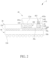
- FIG. 2 is a schematic diagram showing an exemplary semiconductor device according to another embodiment of the invention.
- the semiconductor device 2 may be a System-in-Package (SiP) comprising an application processor (AP) die 30 and a memory die 40 mounted on an upper surface 50a of a package substrate 50 through connecting elements 330 and 430 such as conductive bumps or solder balls.
- the package substrate 50 may comprise a resin core and multiple buildup metal layers on opposite sides of the resin core (not explicitly shown).
- the AP die 30 may have a structure that is similar to the structure of the AP die 10 depicted in FIG. 1 .
- a plurality of connecting elements 530 such as BGA balls may be disposed on a lower surface 50b of the package substrate 50.
- the memory die 40 may comprise a substrate 401 such as a semiconductor substrate.
- the substrate 401 may be a silicon substrate or a SOI substrate, but not limited thereto.
- a circuit structure CS4 may be fabricated on a surface 401a of the substrate 401.
- the circuit structure CS4 may include, but not limited to, active elements such as transistors, passive elements such as resistors, capacitors or inductors, MEMS elements, power circuit elements, and/or interconnect metal layers.
- the circuit structure CS4 may include, but not limited to, logic circuits and/or analog circuits.
- the memory die 40 may comprise a memory structure 402 fabricated on the substrate 401.
- the memory structure 402 may be electrically connected to the circuit structure CS4.
- the memory structure 402 may include, but not limited to, a magneto-resistive random access memory (MRAM) structure, a resistive random access memory (RRAM) structure, a phase-change random access memory (PCRAM) structure, ferroelectric random access memory (FRAM) structure, embedded flash (eflash) memory structure, or the like.
- MRAM magneto-resistive random access memory
- RRAM resistive random access memory
- PCRAM phase-change random access memory
- FRAM ferroelectric random access memory
- flash embedded flash
- the memory die 40 may further comprise at least a deep trench capacitor (DTC) 403 fabricated in the substrate 401.
- DTC deep trench capacitor
- a plurality of DTCs 403 can be formed and connected in parallel to provide large capacitance and to greatly increase the capacitance density, thereby enabling the construction of diverse devices such as higher quality power distribution networks (PDNs).
- PDNs power distribution networks
- the DTC 403 may be covered with a DTC pad 403p.
- a plurality of bond pads 410 and 420 are disposed on an upper surface 40a of the memory die 40.
- the plurality of bond pads 410 and 420 may comprise copper pads, but not limited thereto.
- the bond pads 410 may be NVM pins for transmitting signals such as read, erase, or program signals between the AP die 30 and the memory die 40.
- the bond pad 420 may be a power pin for transmitting power signals.
- the bond pad 420 is electrically connected to the DTC pad 403p through a power supply line PI, thereby reducing chip voltage drop.
- a re-distribution layer (RDL) 460 may be disposed on the upper surface 40a of the memory die 40 to re-distribute or fan-out the bond pads 410 and 420.
- the re-distribution layer 460 may be used to reroute connections to desired locations.
- a bump array located in the center of a chip can be re-distributed to positions near the chip edge.
- the ability to redistribute points can enable higher contact density and enable subsequent packaging steps.
- the re-distribution process adds another set of layers over the wafer surface. A dielectric film is deposited for electrical isolation. The original bond pads are then exposed. Metal lines are deposited to relocate the pads to desired locations, and under bump metallization (UBM) layers are built to support the solder bumps.
- UBM under bump metallization
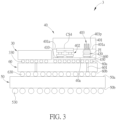
- FIG. 3 is a schematic diagram showing an exemplary semiconductor device according to still another embodiment of the invention, wherein like layers, regions, or elements are designated by like numeral numbers or labels.
- the semiconductor device 3 may be a 2.5D package comprising an application processor (AP) die 30 and a memory die 40 mounted on an upper surface 60a of an interposer substrate 60 in a side-by-side manner through connecting elements 330 and 430, respectively.
- the interposer substrate 60 may be a silicon interposer, but is not limited thereto.
- the interposer substrate 60 may comprise through silicon vias (TSVs) 601.
- the AP die 30 may have a structure that is similar to the structure of the AP die 10 depicted in FIG. 1 .
- the interposer substrate 60 is mounted on an upper surface 50a of a package substrate 50 through connecting elements 630.
- the package substrate 50 may comprise a resin core and multiple buildup layers on opposite sides of the resin core (not explicitly shown).
- a plurality of connecting elements 530 such as BGA balls may be disposed on a lower surface 50b of the package substrate 50.
- the memory die 40 may comprise a substrate 401 such as a semiconductor substrate.
- the substrate 401 may be a silicon substrate or a SOI substrate, but not limited thereto.
- a circuit structure CS4 may be fabricated on a surface 401a of the substrate 401.
- the circuit structure CS4 may include, but not limited to, active elements such as transistors, passive elements such as resistors, capacitors or inductors, MEMS elements, power circuit elements, and/or interconnect metal layers.
- the circuit structure CS4 may include, but not limited to, logic circuits and/or analog circuits.
- the memory die 40 may comprise a memory structure 402 fabricated on the substrate 401.
- the memory structure 402 may be electrically connected to the circuit structure CS4.
- the memory structure 402 may include, but not limited to, a magneto-resistive random access memory (MRAM) structure, a resistive random access memory (RRAM) structure, a phase-change random access memory (PCRAM) structure, ferroelectric random access memory (FRAM) structure, embedded flash (eflash) memory structure, or the like.
- MRAM magneto-resistive random access memory
- RRAM resistive random access memory
- PCRAM phase-change random access memory
- FRAM ferroelectric random access memory
- flash embedded flash
- the memory die 40 may further comprise at least a deep trench capacitor (DTC) 403 fabricated in the substrate 401.
- DTC deep trench capacitor
- a plurality of DTCs 403 can be formed and connected in parallel to provide large capacitance and to greatly increase the capacitance density, thereby enabling the construction of diverse devices such as higher quality power distribution networks (PDNs).
- PDNs power distribution networks
- the DTC 403 may be covered with a DTC pad 403p.
- a plurality of bond pads 410 and 420 are disposed on an upper surface 40a of the memory die 40.
- the plurality of bond pads 410 and 420 may comprise copper pads, but not limited thereto.
- the bond pads 410 may be NVM pins for transmitting signals such as read, erase, or program signals between the AP die 30 and the memory die 40.
- the bond pad 420 may be a power pin for transmitting power signals.
- the bond pad 420 is electrically connected to the DTC pad 403p through a power supply line PI, thereby reducing chip voltage drop.
- a re-distribution layer (RDL) 460 may be disposed on the upper surface 40a of the memory die 40 to re-distribute or fan-out the bond pads 410 and 420.
- the re-distribution layer 460 may be used to reroute connections to desired locations.
- a bump array located in the center of a chip can be re-distributed to positions near the chip edge.
- the ability to redistribute points can enable higher contact density and enable subsequent packaging steps.
- the re-distribution process adds another set of layers over the wafer surface. A dielectric film is deposited for electrical isolation. The original bond pads are then exposed. Metal lines are deposited to relocate the pads to desired locations, and under bump metallization (UBM) layers are built to support the solder bumps.
- UBM under bump metallization
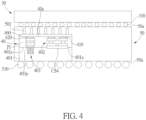
- FIG. 4 is a schematic diagram showing an exemplary semiconductor device according to yet another embodiment of the invention, wherein like layers, regions, or elements are designated by like numeral numbers or labels.
- the semiconductor device 3 may be an embedded die package comprising an application processor (AP) die 30 mounted on an upper surface 50a of a package substrate 50 and a memory die 40 embedded in the package substrate 50.
- the AP die 30 may be mounted on the package substrate 50 through connecting elements 330.
- the memory die 40 may be electrically connected to the AP die 30 or other components on or in the substrate through an interconnect structure 501 such as copper-plated vias and conductive traces of the package substrate 50.
- an interconnect structure 501 such as copper-plated vias and conductive traces of the package substrate 50.
- the package substrate 50 may comprise a resin core and multiple buildup layers on opposite sides of the resin core (not explicitly shown).
- a plurality of connecting elements 530 such as BGA balls may be disposed on a lower surface 50b of the package substrate 50.
- the memory die 40 may comprise a substrate 401 such as a semiconductor substrate.
- the substrate 401 may be a silicon substrate or a SOI substrate, but not limited thereto.
- a circuit structure CS4 may be fabricated on a surface 401a of the substrate 401.
- the circuit structure CS4 may include, but not limited to, active elements such as transistors, passive elements such as resistors, capacitors or inductors, MEMS elements, power circuit elements, and/or interconnect metal layers.
- the circuit structure CS4 may include, but not limited to, logic circuits and/or analog circuits.
- the memory die 40 may comprise a memory structure 402 fabricated on the substrate 401.
- the memory structure 402 may be electrically connected to the circuit structure CS4.
- the memory structure 402 may include, but not limited to, a magneto-resistive random access memory (MRAM) structure, a resistive random access memory (RRAM) structure, a phase-change random access memory (PCRAM) structure, ferroelectric random access memory (FRAM) structure, embedded flash (eflash) memory structure, or the like.
- MRAM magneto-resistive random access memory
- RRAM resistive random access memory
- PCRAM phase-change random access memory
- FRAM ferroelectric random access memory
- flash embedded flash
- the memory die 40 may further comprise at least a deep trench capacitor (DTC) 403 fabricated in the substrate 401.
- DTC deep trench capacitor
- a plurality of DTCs 403 can be formed and connected in parallel to provide large capacitance and to greatly increase the capacitance density, thereby enabling the construction of diverse devices such as higher quality power distribution networks (PDNs).
- PDNs power distribution networks
- the DTC 403 may be covered with a DTC pad 403p.
- a plurality of bond pads 410 and 420 are disposed on an upper surface 40a of the memory die 40.
- the plurality of bond pads 410 and 420 may comprise copper pads, but not limited thereto.
- the bond pads 410 may be NVM pins for transmitting signals such as read, erase, or program signals between the AP die 30 and the memory die 40.
- the bond pad 420 may be a power pin for transmitting power signals.
- the bond pad 420 is electrically connected to the DTC pad 403p through a power supply line PI, thereby reducing chip voltage drop.
- a re-distribution layer (RDL) 460 may be disposed on the upper surface 40a of the memory die 40 to re-distribute or fan-out the bond pads 410 and 420.
- the re-distribution layer 460 may be used to reroute connections to desired locations.
- a bump array located in the center of a chip can be re-distributed to positions near the chip edge.
- the ability to redistribute points can enable higher contact density and enable subsequent packaging steps.
- the re-distribution process adds another set of layers over the wafer surface. A dielectric film is deposited for electrical isolation. The original bond pads are then exposed. Metal lines are deposited to relocate the pads to desired locations, and under bump metallization (UBM) layers are built to support the solder bumps.
- UBM under bump metallization
- the DTCs are integrated with the NVM memory die.
- the size and production cost of the AP die can be reduced.
- the DTCs that function as decoupling capacitors are placed on the power supply line, and therefore the chip voltage drop can be reduced.
Landscapes
- Semiconductor Integrated Circuits (AREA)
- Engineering & Computer Science (AREA)
- Power Engineering (AREA)
- Semiconductor Memories (AREA)
- Internal Circuitry In Semiconductor Integrated Circuit Devices (AREA)
Abstract
Description
- This application claims the benefit of
U.S. Provisional Application No. 63/311,095, filed on February 17th, 2022 - The instant disclosure relates generally to the field of semiconductor technology.
- The rapid advancements in artificial intelligence (AI) are being enabled by advanced GPU's and specialized AI processors utilizing the most advanced silicon process nodes at 5nm.
- High-performance processors require higher steady-state and peak currents with dramatically increasing slew rates, while operating at lower voltages with an increasing number of high-speed I/Os. This trend is accelerating and continually challenging power system designers to ensure delivery of adequate power to the processor core with low loss in the Power Delivery Network (PDN).
- Decoupling capacitors such as metal-insulator-metal (MIM) or high-k based deep trench capacitors (HK DTC) are commonly used to reduce the impedance of a power distribution system. To accommodate the exceedingly demanding power integrity (PI) requirements for the advanced AI and high-performance computing (HPC) components, high-K based deep trench capacitors have been integrated in the silicon interposer with through silicon via (TSV) and fine-pitch interconnects for chip-on-wafer-on-substrate (CoWoS) integration.
- It is desirable to provide high-performance decoupling capacitor to mitigate voltage drop and noise ripple issues and low power memory to reduce power consumption.
- One object of the present invention is to provide an improved semiconductor device with integrated deep trench capacitors in order to solve the above-mentioned prior art problems or shortcomings. Semiconductor devices according to the invention are defined in the independent claims. The dependent claims define preferred embodiments thereof.
- One aspect of the invention provides a semiconductor device including an application processor (AP) die and a memory die directly bonded to the AP die. The memory die includes a substrate, a non-volatile memory structure on the substrate, and at least one trench capacitor in the substrate.
- Preferably, the at least one trench capacitor is a decoupling capacitor.
- Preferably, the non-volatile memory structure comprises a magneto-resistive random access memory (MRAM) structure, a resistive random access memory (RRAM) structure, or a phase-change random access memory (PCRAM) structure.
- Preferably, a first hybrid bond pad and a second hybrid bond pad are disposed on an upper surface of the memory die
- Preferably, the first hybrid bond pad is a memory pin for transmitting signals such as read, erase, or program signals between the AP die and the memory die, and the second hybrid bond pad is a power pin for transmitting power signals.
- Preferably, the at least one trench capacitor is electrically connected to the second hybrid bond pad.
- Preferably, the first and second hybrid bond pads are directly bonded to third and fourth hybrid bond pads on the AP die, respectively, through hybrid bonding.
- Preferably, the first hybrid bond pad, the second hybrid bond pad, the third hybrid bond pad, and the fourth hybrid bond pad are copper pads.
- Preferably, the at least one trench capacitor is connected to a pad.
- Preferably, the second hybrid bond pad is electrically connected to the pad through a power supply line.
- Another aspect of the invention provides a semiconductor device including a package substrate, an application processor (AP) die mounted on the package substrate, and a memory die mounted on the package substrate. The memory die includes a substrate, a non-volatile memory structure on the substrate, and at least one trench capacitor in the substrate.
- Preferably, the at least one trench capacitor is a decoupling capacitor.
- Preferably, the non-volatile memory structure comprises a magneto-resistive random access memory (MRAM) structure, a resistive random access memory (RRAM) structure, or a phase-change random access memory (PCRAM) structure.
- Preferably, a first bond pad and a second bond pad are disposed on an upper surface of the memory die.
- Preferably, the first bond pad is a memory pin for transmitting signals such as read, erase, or program signals between the AP die and the memory die.
- Preferably, the second bond pad is a power pin for transmitting power signals.
- Preferably, the at least one trench capacitor is connected to a pad.
- Preferably, the second bond pad is electrically connected to the pad through a power supply line.
- Preferably, a re-distribution layer is disposed on the upper surface of the memory die.
- Preferably, the memory die is electrically connected to the package substrate through the re-distribution layer.
- Still another aspect of the invention provides a semiconductor device including a package substrate; an interposer substrate on the package substrate; an application processor (AP) die mounted on the interposer substrate; and a memory die mounted on the interposer substrate, wherein the memory die comprises a substrate, a non-volatile memory structure on the substrate, and at least one trench capacitor in the substrate.
- Preferably, the at least one trench capacitor is a decoupling capacitor.
- Preferably, the non-volatile memory structure comprises a magneto-resistive random access memory (MRAM) structure, a resistive random access memory (RRAM) structure, or a phase-change random access memory (PCRAM) structure.
- Preferably, a first bond pad and a second bond pad are disposed on an upper surface of the memory die, wherein the first bond pad is a memory pin for transmitting signals such as read, erase, or program signals between the AP die and the memory die.
- Preferably, the second bond pad is a power pin for transmitting power signals.
- Preferably, the at least one trench capacitor is connected to a pad.
- Preferably, the second bond pad is electrically connected to the pad through a power supply line.
- Preferably, a re-distribution layer is disposed on the upper surface of the memory die.
- Preferably, the memory die is electrically connected to the package substrate through the re-distribution layer.
- Preferably, the interposer substrate is a silicon interposer.
- Still another aspect of the invention provides a semiconductor device including a package substrate; an application processor (AP) die mounted on the package substrate; and a memory die embedded in the package substrate, wherein the memory die comprises a substrate, a non-volatile memory structure on the substrate, and at least one trench capacitor in the substrate.
- Preferably, the memory die is electrically connected to the AP die through an interconnect structure of the package substrate.
- Preferably, the non-volatile memory structure comprises a magneto-resistive random access memory (MRAM) structure, a resistive random access memory (RRAM) structure, or a phase-change random access memory (PCRAM) structure.
- Preferably, a first bond pad and a second bond pad are disposed on an upper surface of the memory die, wherein the first bond pad is a memory pin for transmitting signals such as read, erase, or program signals between the AP die and the memory die.
- Preferably, the second bond pad is a power pin for transmitting power signals.
- Preferably, a re-distribution layer is disposed on the upper surface of the memory die.
- Preferably, the memory die is electrically connected to the package substrate through the re-distribution layer.
- These and other objectives of the present invention will no doubt become obvious to those of ordinary skill in the art after reading the following detailed description of the preferred embodiment that is illustrated in the various figures and drawings.
- The accompanying drawings are included to provide a further understanding of the invention and are incorporated in and constitute a part of this specification. The drawings illustrate embodiments of the invention and, together with the description, serve to explain the principles of the invention. In the drawings:
-
FIG. 1 is a schematic diagram showing an exemplary semiconductor device according to an embodiment of the invention; -
FIG. 2 is a schematic diagram showing an exemplary semiconductor device according to another embodiment of the invention; -
FIG. 3 is a schematic diagram showing an exemplary semiconductor device according to still another embodiment of the invention; and -
FIG. 4 is a schematic diagram showing an exemplary semiconductor device according to yet another embodiment of the invention. - In the following detailed description of embodiments of the invention, reference is made to the accompanying drawings, which form a part hereof, and in which is shown by way of illustration specific preferred embodiments in which the disclosure may be practiced.
- These embodiments are described in sufficient detail to enable those skilled in the art to practice them, and it is to be understood that other embodiments may be utilized and that mechanical, chemical, electrical, and procedural changes may be made without departing from the scope of the present disclosure. The following detailed description is, therefore, not to be taken in a limiting sense, and the scope of embodiments of the present invention is defined only by the appended claims.
- It will be understood that when an element or layer is referred to as being "on", "connected to" or "coupled to" another element or layer, it can be directly on, connected or coupled to the other element or layer or intervening elements or layers may be present. In contrast, when an element is referred to as being "directly on," "directly connected to" or "directly coupled to" another element or layer, there are no intervening elements or layers present. Like numbers refer to like elements throughout. As used herein, the term "and/or" includes any and all combinations of one or more of the associated listed items.
-
FIG. 1 is a schematic diagram showing an exemplary semiconductor device according to an embodiment of the invention. As shown inFIG. 1 , thesemiconductor device 1 comprises an application processor (AP) die 10 directly bonded to amemory die 20 by using a wafer-on-wafer (WoW) technique. Preferably, the AP die 10 comprises asubstrate 101 such as a semiconductor substrate. Preferably, a circuit structure CS1 and a circuit structure CS2 may be fabricated on thesubstrate 101. Preferably, for example, the circuit structure CS1 and the circuit structure CS2 may include, but not limited to, active elements such as transistors, passive elements such as resistors, capacitors or inductors, Micro Electro-Mechanical System (MEMS) elements, power circuit elements, and/or interconnect metal layers. Preferably, for example, the circuit structure CS1 and the circuit structure CS2 may include, but not limited to, logic circuits and/or analog circuits. Preferably, for example, the circuit structure CS1 may be electrically connected to the circuit structure CS2 through an interconnect structure. - Preferably, for example, a plurality of
hybrid bond pads upper surface 10a of the AP die 10. Preferably, for example, the plurality ofhybrid bond pads hybrid bond pads 110 may be non-volatile memory (NVM) pins for transmitting signals such as read, erase, or program signals between the AP die 10 and the memory die 20. Preferably, for example, thehybrid bond pad 120 may be a power pin for transmitting power signals. - Preferably, for example, the memory die 20 may comprise a
substrate 201 such as a semiconductor substrate. Preferably, for example, thesubstrate 201 may be a silicon substrate or a silicon-on-insulator (SOI) substrate, but not limited thereto. Preferably, a circuit structure CS3 may be fabricated on asurface 201a of thesubstrate 201. Preferably, for example, the circuit structure CS3 may include, but not limited to, active elements such as transistors, passive elements such as resistors, capacitors or inductors, MEMS elements, power circuit elements, and/or interconnect metal layers. Preferably, for example, the circuit structure CS3 may include, but not limited to, logic circuits and/or analog circuits. - Preferably, for example, the memory die 20 may comprise a
memory structure 202 fabricated on thesubstrate 201. Preferably, for example, thememory structure 202 may be electrically connected to the circuit structure CS3. Preferably, for example, thememory structure 202 may include, but not limited to, a magneto-resistive random access memory (MRAM) structure, a resistive random access memory (RRAM) structure, a phase-change random access memory (PCRAM) structure, ferroelectric random access memory (FRAM) structure, embedded flash (eflash) memory structure, or the like. - Preferably, for example, the memory die 20 may further comprise at least a deep trench capacitor (DTC) 203 fabricated in the
substrate 201. Preferably, for example, theDTC 203 is a decoupling capacitor. Preferably, for example, a plurality ofDTCs 203 can be formed and connected in parallel to provide large capacitance and to greatly increase the capacitance density, thereby enabling the construction of diverse devices such as higher quality power distribution networks (PDNs). - The fabrication of the
DTC 203 is known in the art. For example, a deep trench may be etched into thesubstrate 201. A bottom electrode may be conformally formed in the deep trench. A dielectric layer such as a high k dielectric may be formed to coat the bottom electrode layer by physical vapor deposition (PVD), such as sputtering or pulsed laser deposition, or chemical vapor deposition (CVD), such as MOCVD. A top electrode layer is then formed to fill the remaining space in the deep trench by PVD such as sputtering or pulsed laser deposition or CVD such as MOCVD. For example, theDTC 203 may be high-frequency capacitor that may be used to decouple very high-frequency currents (>10MHz). Preferably, for example, theDTC 203 may be connected to aDTC pad 203p such as a copper pad. - Preferably, for example, a plurality of
hybrid bond pads upper surface 20a of the memory die 20. Preferably, for example, the plurality ofhybrid bond pads hybrid bond pads 210 may be NVM pins for transmitting signals such as read, erase, or program signals between the AP die 10 and the memory die 20. Preferably, for example, thehybrid bond pad 220 may be a power pin for transmitting power signals. Preferably, for example, thehybrid bond pad 220 is electrically connected to theDTC pad 203p through a power supply line PI, thereby reducing chip voltage drop. - Preferably, for example, the
hybrid bond pads hybrid bond pads hybrid bond pads hybrid bond pads hybrid bond pads hybrid bond pads -
FIG. 2 is a schematic diagram showing an exemplary semiconductor device according to another embodiment of the invention. As shown inFIG. 2 , thesemiconductor device 2 may be a System-in-Package (SiP) comprising an application processor (AP) die 30 and amemory die 40 mounted on anupper surface 50a of apackage substrate 50 through connectingelements package substrate 50 may comprise a resin core and multiple buildup metal layers on opposite sides of the resin core (not explicitly shown). Preferably, the AP die 30 may have a structure that is similar to the structure of the AP die 10 depicted inFIG. 1 . Preferably, a plurality of connectingelements 530 such as BGA balls may be disposed on alower surface 50b of thepackage substrate 50. - Preferably, for example, the memory die 40 may comprise a
substrate 401 such as a semiconductor substrate. Preferably, for example, thesubstrate 401 may be a silicon substrate or a SOI substrate, but not limited thereto. Preferably, a circuit structure CS4 may be fabricated on asurface 401a of thesubstrate 401. Preferably, for example, the circuit structure CS4 may include, but not limited to, active elements such as transistors, passive elements such as resistors, capacitors or inductors, MEMS elements, power circuit elements, and/or interconnect metal layers. Preferably, for example, the circuit structure CS4 may include, but not limited to, logic circuits and/or analog circuits. - Preferably, for example, the memory die 40 may comprise a
memory structure 402 fabricated on thesubstrate 401. Preferably, for example, thememory structure 402 may be electrically connected to the circuit structure CS4. Preferably, for example, thememory structure 402 may include, but not limited to, a magneto-resistive random access memory (MRAM) structure, a resistive random access memory (RRAM) structure, a phase-change random access memory (PCRAM) structure, ferroelectric random access memory (FRAM) structure, embedded flash (eflash) memory structure, or the like. - Preferably, for example, the memory die 40 may further comprise at least a deep trench capacitor (DTC) 403 fabricated in the
substrate 401. Preferably, for example, a plurality ofDTCs 403 can be formed and connected in parallel to provide large capacitance and to greatly increase the capacitance density, thereby enabling the construction of diverse devices such as higher quality power distribution networks (PDNs). Preferably, for example, theDTC 403 may be covered with aDTC pad 403p. - Preferably, for example, a plurality of
bond pads upper surface 40a of the memory die 40. Preferably, for example, the plurality ofbond pads bond pads 410 may be NVM pins for transmitting signals such as read, erase, or program signals between the AP die 30 and the memory die 40. Preferably, for example, thebond pad 420 may be a power pin for transmitting power signals. Preferably, for example, thebond pad 420 is electrically connected to theDTC pad 403p through a power supply line PI, thereby reducing chip voltage drop. - Preferably, for example, a re-distribution layer (RDL) 460 may be disposed on the
upper surface 40a of the memory die 40 to re-distribute or fan-out thebond pads re-distribution layer 460 may be used to reroute connections to desired locations. For example, a bump array located in the center of a chip can be re-distributed to positions near the chip edge. The ability to redistribute points can enable higher contact density and enable subsequent packaging steps. The re-distribution process adds another set of layers over the wafer surface. A dielectric film is deposited for electrical isolation. The original bond pads are then exposed. Metal lines are deposited to relocate the pads to desired locations, and under bump metallization (UBM) layers are built to support the solder bumps. -
FIG. 3 is a schematic diagram showing an exemplary semiconductor device according to still another embodiment of the invention, wherein like layers, regions, or elements are designated by like numeral numbers or labels. As shown inFIG. 3 , thesemiconductor device 3 may be a 2.5D package comprising an application processor (AP) die 30 and amemory die 40 mounted on anupper surface 60a of aninterposer substrate 60 in a side-by-side manner through connectingelements interposer substrate 60 may be a silicon interposer, but is not limited thereto. Preferably, for example, theinterposer substrate 60 may comprise through silicon vias (TSVs) 601. Preferably, the AP die 30 may have a structure that is similar to the structure of the AP die 10 depicted inFIG. 1 . Theinterposer substrate 60 is mounted on anupper surface 50a of apackage substrate 50 through connectingelements 630. Preferably, for example, thepackage substrate 50 may comprise a resin core and multiple buildup layers on opposite sides of the resin core (not explicitly shown). Preferably, a plurality of connectingelements 530 such as BGA balls may be disposed on alower surface 50b of thepackage substrate 50. - Preferably, likewise, the memory die 40 may comprise a
substrate 401 such as a semiconductor substrate. Preferably, for example, thesubstrate 401 may be a silicon substrate or a SOI substrate, but not limited thereto. Preferably, a circuit structure CS4 may be fabricated on asurface 401a of thesubstrate 401. Preferably, for example, the circuit structure CS4 may include, but not limited to, active elements such as transistors, passive elements such as resistors, capacitors or inductors, MEMS elements, power circuit elements, and/or interconnect metal layers. Preferably, for example, the circuit structure CS4 may include, but not limited to, logic circuits and/or analog circuits. - Preferably, for example, the memory die 40 may comprise a
memory structure 402 fabricated on thesubstrate 401. Preferably, for example, thememory structure 402 may be electrically connected to the circuit structure CS4. Preferably, for example, thememory structure 402 may include, but not limited to, a magneto-resistive random access memory (MRAM) structure, a resistive random access memory (RRAM) structure, a phase-change random access memory (PCRAM) structure, ferroelectric random access memory (FRAM) structure, embedded flash (eflash) memory structure, or the like. - Preferably, for example, the memory die 40 may further comprise at least a deep trench capacitor (DTC) 403 fabricated in the
substrate 401. Preferably, for example, a plurality ofDTCs 403 can be formed and connected in parallel to provide large capacitance and to greatly increase the capacitance density, thereby enabling the construction of diverse devices such as higher quality power distribution networks (PDNs). Preferably, for example, theDTC 403 may be covered with aDTC pad 403p. - Preferably, for example, a plurality of
bond pads upper surface 40a of the memory die 40. Preferably, for example, the plurality ofbond pads bond pads 410 may be NVM pins for transmitting signals such as read, erase, or program signals between the AP die 30 and the memory die 40. Preferably, for example, thebond pad 420 may be a power pin for transmitting power signals. Preferably, for example, thebond pad 420 is electrically connected to theDTC pad 403p through a power supply line PI, thereby reducing chip voltage drop. - Preferably, for example, a re-distribution layer (RDL) 460 may be disposed on the
upper surface 40a of the memory die 40 to re-distribute or fan-out thebond pads re-distribution layer 460 may be used to reroute connections to desired locations. For example, a bump array located in the center of a chip can be re-distributed to positions near the chip edge. The ability to redistribute points can enable higher contact density and enable subsequent packaging steps. The re-distribution process adds another set of layers over the wafer surface. A dielectric film is deposited for electrical isolation. The original bond pads are then exposed. Metal lines are deposited to relocate the pads to desired locations, and under bump metallization (UBM) layers are built to support the solder bumps. -
FIG. 4 is a schematic diagram showing an exemplary semiconductor device according to yet another embodiment of the invention, wherein like layers, regions, or elements are designated by like numeral numbers or labels. As shown inFIG. 4 , thesemiconductor device 3 may be an embedded die package comprising an application processor (AP) die 30 mounted on anupper surface 50a of apackage substrate 50 and amemory die 40 embedded in thepackage substrate 50. The AP die 30 may be mounted on thepackage substrate 50 through connectingelements 330. The memory die 40 may be electrically connected to the AP die 30 or other components on or in the substrate through aninterconnect structure 501 such as copper-plated vias and conductive traces of thepackage substrate 50. Preferably, for example, thepackage substrate 50 may comprise a resin core and multiple buildup layers on opposite sides of the resin core (not explicitly shown). Preferably, a plurality of connectingelements 530 such as BGA balls may be disposed on alower surface 50b of thepackage substrate 50. - Preferably, likewise, the memory die 40 may comprise a
substrate 401 such as a semiconductor substrate. Preferably, for example, thesubstrate 401 may be a silicon substrate or a SOI substrate, but not limited thereto. Preferably, a circuit structure CS4 may be fabricated on asurface 401a of thesubstrate 401. Preferably, for example, the circuit structure CS4 may include, but not limited to, active elements such as transistors, passive elements such as resistors, capacitors or inductors, MEMS elements, power circuit elements, and/or interconnect metal layers. Preferably, for example, the circuit structure CS4 may include, but not limited to, logic circuits and/or analog circuits. - Preferably, for example, the memory die 40 may comprise a
memory structure 402 fabricated on thesubstrate 401. Preferably, for example, thememory structure 402 may be electrically connected to the circuit structure CS4. Preferably, for example, thememory structure 402 may include, but not limited to, a magneto-resistive random access memory (MRAM) structure, a resistive random access memory (RRAM) structure, a phase-change random access memory (PCRAM) structure, ferroelectric random access memory (FRAM) structure, embedded flash (eflash) memory structure, or the like. - Preferably, for example, the memory die 40 may further comprise at least a deep trench capacitor (DTC) 403 fabricated in the
substrate 401. Preferably, for example, a plurality ofDTCs 403 can be formed and connected in parallel to provide large capacitance and to greatly increase the capacitance density, thereby enabling the construction of diverse devices such as higher quality power distribution networks (PDNs). Preferably, for example, theDTC 403 may be covered with aDTC pad 403p. - Preferably, for example, a plurality of
bond pads upper surface 40a of the memory die 40. Preferably, for example, the plurality ofbond pads bond pads 410 may be NVM pins for transmitting signals such as read, erase, or program signals between the AP die 30 and the memory die 40. Preferably, for example, thebond pad 420 may be a power pin for transmitting power signals. Preferably, for example, thebond pad 420 is electrically connected to theDTC pad 403p through a power supply line PI, thereby reducing chip voltage drop. - Preferably, for example, a re-distribution layer (RDL) 460 may be disposed on the
upper surface 40a of the memory die 40 to re-distribute or fan-out thebond pads re-distribution layer 460 may be used to reroute connections to desired locations. For example, a bump array located in the center of a chip can be re-distributed to positions near the chip edge. The ability to redistribute points can enable higher contact density and enable subsequent packaging steps. The re-distribution process adds another set of layers over the wafer surface. A dielectric film is deposited for electrical isolation. The original bond pads are then exposed. Metal lines are deposited to relocate the pads to desired locations, and under bump metallization (UBM) layers are built to support the solder bumps. - It is advantageous to use the instant application because the DTCs are integrated with the NVM memory die. The size and production cost of the AP die can be reduced. Further, the DTCs that function as decoupling capacitors are placed on the power supply line, and therefore the chip voltage drop can be reduced.
- Those skilled in the art will readily observe that numerous modifications and alterations of the device and method may be made while retaining the teachings of the invention. Accordingly, the above disclosure should be construed as limited only by the metes and bounds of the appended claims.
Claims (15)
- A semiconductor device (1), comprising:an application processor, in the following also referred to as AP, die (10); anda memory die (20) directly bonded to the AP die (10), wherein the memory die (20) comprises a substrate (201), a non-volatile memory structure (202) on the substrate (201), and at least one trench capacitor (203) in the substrate (201).
- A semiconductor device (2), comprising:a package substrate (50);an application processor, in the following also referred to as AP, die (30) mounted on the package substrate (50); anda memory die (40) mounted on the package substrate (50) or embedded in the package substrate (50), wherein the memory die (40) comprises a substrate (401), a non-volatile memory structure (402) on the substrate (401), and at least one trench capacitor (403) in the substrate (401).
- A semiconductor device (3), comprising:a package substrate (50);an interposer substrate (60) on the package substrate (50);an application processor, in the following also referred to as AP, die (30) mounted on the interposer substrate (60); anda memory die (40) mounted on the interposer substrate (60), wherein the memory die (40) comprises a substrate (401), a non-volatile memory structure (402) on the substrate (401), and at least one trench capacitor (403) in the substrate (401).
- The semiconductor device (1; 2; 3) according to any one of claims 1 to 3, wherein the at least one trench capacitor (203; 403) is a decoupling capacitor.
- The semiconductor device (1; 2; 3) according to any one of claims 1 to 4, wherein the non-volatile memory structure (202; 402) comprises a magneto-resistive random access memory, in the following also referred to as MRAM, structure, a resistive random access memory, in the following also referred to as RRAM, structure, a ferroelectric random access memory, in the following also referred to as FRAM, structure, an embedded flash, in the following also referred to as eflash, memory structure, or a phase-change random access memory, in the following also referred to as PCRAM, structure.
- The semiconductor device (1; 2; 3) according to any one of claims 1 to 5, wherein a first bond pad (210; 410) and a second bond pad (220; 420) are disposed on an upper surface (20a; 40a) of the memory die (20; 40), wherein the first bond pad (210) and the second bond pad (220) are preferably hybrid bond pads.
- The semiconductor device (1; 2; 3) according to claim 6, wherein the first bond pad (210; 410) is a memory pin for transmitting signals such as read, erase, or program signals between the AP die (10; 30) and the memory die (20; 40).
- The semiconductor device (1; 2; 3) according to claim 6 or 7, wherein the second bond pad (220; 420) is a power pin for transmitting power signals.
- The semiconductor device (1) according to any one of claims 6 to 8, wherein the first and second bond pads (210; 220) are directly bonded to third and fourth bond pads (110; 120) on the AP die (10), respectively, preferably through hybrid bonding;
wherein preferably the first bond pad (210), the second bond pad (220), the third bond pad (110), and the fourth bond pad (120) are copper pads and/or hybrid bond pads. - The semiconductor device (1; 2; 3) according to any one of claims 1 to 9, wherein the at least one trench capacitor (203; 403) is connected to a pad (203p; 403p); and/or
wherein the at least one trench capacitor (203; 403) is electrically connected to the second bond pad (220; 420). - The semiconductor device (1; 2; 3) according to claim 10, wherein the second bond pad (220; 420) is electrically connected to the pad (203p; 403p) through a power supply line (PI).
- The semiconductor device (2; 3) according to any one of claims 2, 3, and 4 to 11 being directly or indirectly dependent on claim 2 or 3, wherein a re-distribution layer (460) is disposed on the upper surface of the memory die (40).
- The semiconductor device (2; 3) according to claim 12, wherein the memory die (40) is electrically connected to the package substrate (50) through the re-distribution layer (460).
- The semiconductor device (3) according to any one of claims 3 and 4 to 13 being directly or indirectly dependent on claim 3, wherein the interposer substrate (60) is a silicon interposer.
- The semiconductor device according to any one of claims 2, 3, and 4 to 14 being directly or indirectly dependent on claim 2 or 3, wherein the memory die (40) is electrically connected to the AP die (30) through an interconnect structure (501) of the package substrate (50).
Applications Claiming Priority (2)
| Application Number | Priority Date | Filing Date | Title |
|---|---|---|---|
| US202263311095P | 2022-02-17 | 2022-02-17 | |
| US18/097,296 US20230260894A1 (en) | 2022-02-17 | 2023-01-16 | Semiconductor device with integrated deep trench capacitors |
Publications (1)
| Publication Number | Publication Date |
|---|---|
| EP4243066A1 true EP4243066A1 (en) | 2023-09-13 |
Family
ID=85225250
Family Applications (1)
| Application Number | Title | Priority Date | Filing Date |
|---|---|---|---|
| EP23155718.2A Pending EP4243066A1 (en) | 2022-02-17 | 2023-02-09 | Semiconductor device with integrated deep trench capacitors |
Country Status (3)
| Country | Link |
|---|---|
| US (1) | US20230260894A1 (en) |
| EP (1) | EP4243066A1 (en) |
| TW (1) | TWI852319B (en) |
Families Citing this family (3)
| Publication number | Priority date | Publication date | Assignee | Title |
|---|---|---|---|---|
| US12400926B2 (en) * | 2022-05-25 | 2025-08-26 | Taiwan Semiconductor Manufacturing Company, Ltd. | Semiconductor device and method of manufacture |
| US20240234295A9 (en) * | 2022-10-19 | 2024-07-11 | Mediatek Inc. | Semiconductor package structure |
| CN120379274A (en) * | 2024-04-28 | 2025-07-25 | 北京玄戒技术有限公司 | Chip and electronic device |
Citations (2)
| Publication number | Priority date | Publication date | Assignee | Title |
|---|---|---|---|---|
| US20150049537A1 (en) * | 2013-08-19 | 2015-02-19 | SK Hynix Inc. | Electronic device and method for fabricating the same |
| US20190164905A1 (en) * | 2017-11-29 | 2019-05-30 | Taiwan Semiconductor Manufacturing Co., Ltd. | Semiconductor device and method of making the same |
Family Cites Families (45)
| Publication number | Priority date | Publication date | Assignee | Title |
|---|---|---|---|---|
| US5880991A (en) * | 1997-04-14 | 1999-03-09 | International Business Machines Corporation | Structure for low cost mixed memory integration, new NVRAM structure, and process for forming the mixed memory and NVRAM structure |
| US7098070B2 (en) * | 2004-11-16 | 2006-08-29 | International Business Machines Corporation | Device and method for fabricating double-sided SOI wafer scale package with through via connections |
| US20080153200A1 (en) * | 2006-12-22 | 2008-06-26 | Arkalgud Sitaram | Stacked semiconductor components |
| US7875529B2 (en) * | 2007-10-05 | 2011-01-25 | Micron Technology, Inc. | Semiconductor devices |
| US20150001675A1 (en) * | 2008-09-17 | 2015-01-01 | Mediatek Inc. | Method for including decoupling capacitors into semiconductor circuit having logic circuit therein and semiconductor circuit thereof |
| US8609486B1 (en) * | 2012-01-06 | 2013-12-17 | Altera Corporation | Methods for fabricating deep trench capacitors |
| KR20150042612A (en) * | 2013-10-11 | 2015-04-21 | 삼성전자주식회사 | Semiconductor device having decoupling capacitor and method of forming the same |
| US9153504B2 (en) * | 2013-10-11 | 2015-10-06 | Taiwan Semiconductor Manufacturing Company, Ltd. | Metal insulator metal capacitor and method for making the same |
| US9331062B1 (en) * | 2013-12-06 | 2016-05-03 | Altera Corporation | Integrated circuits with backside power delivery |
| US9413169B2 (en) * | 2014-04-02 | 2016-08-09 | Globalfoundries Inc. | Electrostatic discharge protection circuit with a fail-safe mechanism |
| US9209172B2 (en) * | 2014-05-08 | 2015-12-08 | International Business Machines Corporation | FinFET and fin-passive devices |
| US9922970B2 (en) * | 2015-02-13 | 2018-03-20 | Qualcomm Incorporated | Interposer having stacked devices |
| US9679909B2 (en) * | 2015-06-25 | 2017-06-13 | Taiwan Samiconductor Manufacturing Co., Ltd. | Method for manufacturing a finger trench capacitor with a split-gate flash memory cell |
| US10276651B2 (en) * | 2017-09-01 | 2019-04-30 | Taiwan Semiconductor Manufacturing Co., Ltd. | Low warpage high density trench capacitor |
| JP7109795B2 (en) * | 2017-09-01 | 2022-08-01 | 国立大学法人静岡大学 | Semiconductor device and its manufacturing method |
| US10510738B2 (en) * | 2018-01-17 | 2019-12-17 | Sandisk Technologies Llc | Three-dimensional memory device having support-die-assisted source power distribution and method of making thereof |
| US10559650B2 (en) * | 2018-01-23 | 2020-02-11 | Texas Instruments Incorporated | Trench capacitor with warpage reduction |
| KR102362622B1 (en) * | 2018-02-23 | 2022-02-14 | 삼성전자주식회사 | Semiconductor device including different types of memory cells |
| US20200006367A1 (en) * | 2018-05-09 | 2020-01-02 | Irvine Sensors Corporation | 3D-Stacked Module with Unlimited Scalable Memory Architecture for Very High Bandwidth and Very High Capacity Data Processing Devices |
| US11380614B2 (en) * | 2018-12-26 | 2022-07-05 | AP Memory Technology Corp. | Circuit assembly |
| US11462270B2 (en) * | 2018-12-31 | 2022-10-04 | Samsung Electronics Co., Ltd. | Nonvolatile memory device and memory system including the same |
| WO2020210928A1 (en) * | 2019-04-15 | 2020-10-22 | Yangtze Memory Technologies Co., Ltd. | Integration of three-dimensional nand memory devices with multiple functional chips |
| WO2020220280A1 (en) * | 2019-04-30 | 2020-11-05 | Yangtze Memory Technologies Co., Ltd. | Three-dimensional memory device with embedded dynamic random-access memory |
| WO2020211272A1 (en) * | 2019-04-15 | 2020-10-22 | Yangtze Memory Technologies Co., Ltd. | Unified semiconductor devices having processor and heterogeneous memories and methods for forming the same |
| US11201205B2 (en) * | 2019-07-31 | 2021-12-14 | Taiwan Semiconductor Manufacturing Company, Ltd. | Interconnect layout for semiconductor device |
| US11296099B2 (en) * | 2019-07-31 | 2022-04-05 | Taiwan Semiconductor Manufacturing Company, Ltd. | FeRAM decoupling capacitor |
| US11329057B2 (en) * | 2019-08-30 | 2022-05-10 | Samsung Electronics Co., Ltd. | Integrated circuit device |
| US11671010B2 (en) * | 2020-02-07 | 2023-06-06 | Taiwan Semiconductor Manufacturing Company, Ltd. | Power delivery for multi-chip-package using in-package voltage regulator |
| US11316027B2 (en) * | 2020-03-27 | 2022-04-26 | Intel Corporation | Relaxor ferroelectric capacitors and methods of fabrication |
| US11581281B2 (en) * | 2020-06-26 | 2023-02-14 | Taiwan Semiconductor Manufacturing Co., Ltd. | Packaged semiconductor device and method of forming thereof |
| US11769731B2 (en) * | 2021-01-14 | 2023-09-26 | Taiwan Semiconductor Manufacturing Co., Ltd | Architecture for computing system package |
| US12294033B2 (en) * | 2021-05-15 | 2025-05-06 | Taiwan Semiconductor Manufacturing Company, Ltd. | Deep trench capacitor array with reduced warpage |
| US12310001B2 (en) * | 2021-06-25 | 2025-05-20 | Intel Corporation | Decoupling capacitors and methods of fabrication |
| WO2023070637A1 (en) * | 2021-10-31 | 2023-05-04 | Yangtze Memory Technologies Co., Ltd. | Memory devices having vertical transistors and stacked storage units and methods for forming thereof |
| US20230207445A1 (en) * | 2021-12-23 | 2023-06-29 | Abhishek Anil Sharma | High bandwidth and capacity approaches for stitched dies |
| US20230260977A1 (en) * | 2022-02-17 | 2023-08-17 | Mediatek Inc. | Semiconductor packages |
| EP4461105A4 (en) * | 2022-05-19 | 2025-06-18 | Yangtze Memory Technologies Co., Ltd. | MEMORY DEVICES COMPRISING VERTICAL TRANSISTORS AND METHODS OF FORMING THE SAME |
| US20240030359A1 (en) * | 2022-07-21 | 2024-01-25 | Taiwan Semiconductor Manufacturing Company Ltd. | Semiconductor device with capacitor and method for forming the same |
| US12381150B2 (en) * | 2022-07-21 | 2025-08-05 | Advanced Semiconductor Engineering, Inc. | Electronic device |
| US20240063148A1 (en) * | 2022-08-17 | 2024-02-22 | Intel Corporation | Deep trench capacitor bridge for multi-chip package |
| US20240128193A1 (en) * | 2022-10-14 | 2024-04-18 | Advanced Semiconductor Engineering, Inc. | Electronic module and electronic apparatus |
| US20240224542A1 (en) * | 2022-12-28 | 2024-07-04 | Xilinx, Inc. | Programmable hybrid memory and capacitive device in a dram process |
| US20240222326A1 (en) * | 2022-12-30 | 2024-07-04 | Intel Corporation | Package architecture with memory chips having different process regions |
| US20240222328A1 (en) * | 2022-12-30 | 2024-07-04 | Intel Corporation | Package architecture with memory chips having different process regions |
| US20250219021A1 (en) * | 2023-12-27 | 2025-07-03 | Intel Corporation | Vertically embedded components in package substrates |
-
2023
- 2023-01-16 US US18/097,296 patent/US20230260894A1/en active Pending
- 2023-02-06 TW TW112104074A patent/TWI852319B/en active
- 2023-02-09 EP EP23155718.2A patent/EP4243066A1/en active Pending
Patent Citations (2)
| Publication number | Priority date | Publication date | Assignee | Title |
|---|---|---|---|---|
| US20150049537A1 (en) * | 2013-08-19 | 2015-02-19 | SK Hynix Inc. | Electronic device and method for fabricating the same |
| US20190164905A1 (en) * | 2017-11-29 | 2019-05-30 | Taiwan Semiconductor Manufacturing Co., Ltd. | Semiconductor device and method of making the same |
Non-Patent Citations (2)
| Title |
|---|
| ZHANG XIAOWU ET AL: "Heterogeneous 2.5D integration on through silicon interposer", APPLIED PHYSICS REVIEWS, vol. 2, no. 2, 1 June 2015 (2015-06-01), pages 021308, XP055776606, DOI: 10.1063/1.4921463 * |
| ZHE LI ET AL: "Development of an optimized power delivery system for 3D IC integration with TSV silicon interposer", ELECTRONIC COMPONENTS AND TECHNOLOGY CONFERENCE (ECTC), 2012 IEEE 62ND, IEEE, 29 May 2012 (2012-05-29), pages 678 - 682, XP032210658, ISBN: 978-1-4673-1966-9, DOI: 10.1109/ECTC.2012.6248905 * |
Also Published As
| Publication number | Publication date |
|---|---|
| TW202335220A (en) | 2023-09-01 |
| TWI852319B (en) | 2024-08-11 |
| US20230260894A1 (en) | 2023-08-17 |
Similar Documents
| Publication | Publication Date | Title |
|---|---|---|
| US20230260894A1 (en) | Semiconductor device with integrated deep trench capacitors | |
| US8387240B2 (en) | Methods for making multi-chip packaging using an interposer | |
| US8928132B2 (en) | Semiconductor package having through silicon via (TSV) interposer and method of manufacturing the semiconductor package | |
| CN114937657B (en) | Methods and systems for improving power delivery and signaling in stacked semiconductor devices | |
| US7882628B2 (en) | Multi-chip packaging using an interposer such as a silicon based interposer with through-silicon-vias | |
| US10763242B2 (en) | Semiconductor package and method of manufacturing the same | |
| US20130075905A1 (en) | Semiconductor Chips and Semiconductor Packages and Methods of Fabricating the Same | |
| CN107464804A (en) | Semiconductor packages and its manufacture method including radiator | |
| CN115394768B (en) | A multi-layer high bandwidth memory and a manufacturing method thereof | |
| TWI708293B (en) | Semiconductor packages including through mold ball connectors on elevated pads and methods of manufacturing the same | |
| TWI832249B (en) | Capacitor structure, semiconductor structure, and method for manufacturing thereof | |
| CN118782595A (en) | Semiconductor packaging structure and preparation method, storage system | |
| US12482764B2 (en) | Semiconductor package including power plane connecting power terminal of passive device unit and dummy bump of interposer | |
| US20120168933A1 (en) | Wafer level molding structure | |
| EP4489072A1 (en) | Semiconductor device including interconnect package with capacitor embedded therein | |
| US20250087634A1 (en) | Semiconductor packages and methods for manufacturing the same | |
| CN116613155A (en) | Semiconductor device with a semiconductor layer having a plurality of semiconductor layers | |
| CN118073321A (en) | Packaging structure and packaging method | |
| TWI904874B (en) | Semiconductor packages and methods of fabricating thereof | |
| US20250203889A1 (en) | Silicon substrate semiconductor package with integrated stack capacitor and method of manufacturing the same | |
| US20250022860A1 (en) | Semiconductor package and method for manufacturing the same | |
| US20260068702A1 (en) | Semiconductor structure and method of forming the same | |
| US20220130781A1 (en) | Circuit substrate structure and manufacturing method thereof | |
| Garrou et al. | Three‐Dimensional Integration | |
| WO2025025584A1 (en) | Chip stacking structure, electronic apparatus, and preparation method for chip stacking structure |
Legal Events
| Date | Code | Title | Description |
|---|---|---|---|
| PUAI | Public reference made under article 153(3) epc to a published international application that has entered the european phase |
Free format text: ORIGINAL CODE: 0009012 |
|
| STAA | Information on the status of an ep patent application or granted ep patent |
Free format text: STATUS: THE APPLICATION HAS BEEN PUBLISHED |
|
| AK | Designated contracting states |
Kind code of ref document: A1 Designated state(s): AL AT BE BG CH CY CZ DE DK EE ES FI FR GB GR HR HU IE IS IT LI LT LU LV MC ME MK MT NL NO PL PT RO RS SE SI SK SM TR |
|
| STAA | Information on the status of an ep patent application or granted ep patent |
Free format text: STATUS: REQUEST FOR EXAMINATION WAS MADE |
|
| 17P | Request for examination filed |
Effective date: 20240312 |
|
| RBV | Designated contracting states (corrected) |
Designated state(s): AL AT BE BG CH CY CZ DE DK EE ES FI FR GB GR HR HU IE IS IT LI LT LU LV MC ME MK MT NL NO PL PT RO RS SE SI SK SM TR |