EP4240129A1 - Display apparatus - Google Patents
Display apparatus Download PDFInfo
- Publication number
- EP4240129A1 EP4240129A1 EP23158757.7A EP23158757A EP4240129A1 EP 4240129 A1 EP4240129 A1 EP 4240129A1 EP 23158757 A EP23158757 A EP 23158757A EP 4240129 A1 EP4240129 A1 EP 4240129A1
- Authority
- EP
- European Patent Office
- Prior art keywords
- well
- auxiliary
- area
- layer
- display apparatus
- Prior art date
- Legal status (The legal status is an assumption and is not a legal conclusion. Google has not performed a legal analysis and makes no representation as to the accuracy of the status listed.)
- Pending
Links
Images




Classifications
-
- H—ELECTRICITY
- H10—SEMICONDUCTOR DEVICES; ELECTRIC SOLID-STATE DEVICES NOT OTHERWISE PROVIDED FOR
- H10K—ORGANIC ELECTRIC SOLID-STATE DEVICES
- H10K59/00—Integrated devices, or assemblies of multiple devices, comprising at least one organic light-emitting element covered by group H10K50/00
- H10K59/30—Devices specially adapted for multicolour light emission
- H10K59/38—Devices specially adapted for multicolour light emission comprising colour filters or colour changing media [CCM]
-
- H—ELECTRICITY
- H10—SEMICONDUCTOR DEVICES; ELECTRIC SOLID-STATE DEVICES NOT OTHERWISE PROVIDED FOR
- H10K—ORGANIC ELECTRIC SOLID-STATE DEVICES
- H10K59/00—Integrated devices, or assemblies of multiple devices, comprising at least one organic light-emitting element covered by group H10K50/00
- H10K59/10—OLED displays
- H10K59/12—Active-matrix OLED [AMOLED] displays
- H10K59/122—Pixel-defining structures or layers, e.g. banks
-
- H—ELECTRICITY
- H10—SEMICONDUCTOR DEVICES; ELECTRIC SOLID-STATE DEVICES NOT OTHERWISE PROVIDED FOR
- H10K—ORGANIC ELECTRIC SOLID-STATE DEVICES
- H10K50/00—Organic light-emitting devices
- H10K50/80—Constructional details
- H10K50/805—Electrodes
-
- H—ELECTRICITY
- H10—SEMICONDUCTOR DEVICES; ELECTRIC SOLID-STATE DEVICES NOT OTHERWISE PROVIDED FOR
- H10K—ORGANIC ELECTRIC SOLID-STATE DEVICES
- H10K50/00—Organic light-emitting devices
- H10K50/80—Constructional details
- H10K50/84—Passivation; Containers; Encapsulations
- H10K50/842—Containers
- H10K50/8428—Vertical spacers, e.g. arranged between the sealing arrangement and the OLED
-
- H—ELECTRICITY
- H10—SEMICONDUCTOR DEVICES; ELECTRIC SOLID-STATE DEVICES NOT OTHERWISE PROVIDED FOR
- H10K—ORGANIC ELECTRIC SOLID-STATE DEVICES
- H10K59/00—Integrated devices, or assemblies of multiple devices, comprising at least one organic light-emitting element covered by group H10K50/00
- H10K59/50—OLEDs integrated with light modulating elements, e.g. with electrochromic elements, photochromic elements or liquid crystal elements
-
- H—ELECTRICITY
- H10—SEMICONDUCTOR DEVICES; ELECTRIC SOLID-STATE DEVICES NOT OTHERWISE PROVIDED FOR
- H10K—ORGANIC ELECTRIC SOLID-STATE DEVICES
- H10K59/00—Integrated devices, or assemblies of multiple devices, comprising at least one organic light-emitting element covered by group H10K50/00
- H10K59/80—Constructional details
- H10K59/875—Arrangements for extracting light from the devices
- H10K59/879—Arrangements for extracting light from the devices comprising refractive means, e.g. lenses
-
- H—ELECTRICITY
- H10—SEMICONDUCTOR DEVICES; ELECTRIC SOLID-STATE DEVICES NOT OTHERWISE PROVIDED FOR
- H10K—ORGANIC ELECTRIC SOLID-STATE DEVICES
- H10K2102/00—Constructional details relating to the organic devices covered by this subclass
- H10K2102/301—Details of OLEDs
- H10K2102/331—Nanoparticles used in non-emissive layers, e.g. in packaging layer
Definitions
- the present invention relates to a display apparatus.
- a display apparatus includes a plurality of pixels.
- each pixel may emit light of a different color.
- at least some pixels of the display apparatus include a color conversion unit. Accordingly, light having a wavelength in a first wavelength band generated by a light emitter of some pixels may be converted into light having a wavelength in a second wavelength band while passing through a corresponding color conversion unit and may be extracted to the outside.
- the present invention relates to a display apparatus, and for example, to a display apparatus capable of reducing the risk of defects in a manufacturing process.
- a display apparatus may have a problem in that defects are likely to occur in a manufacturing process.
- Embodiments of the present invention include a display apparatus that may have a relatively reduced risk of defects in a manufacturing process.
- the detailed embodiments are examples, and do not limit the scope of the disclosure.
- a display apparatus comprises the features of claim 1.
- the dependent claims describe preferred embodiments. Additional aspects will be set forth in part in the description which follows and, in part, will be apparent from the description, or may be learned by practice of the presented embodiments.
- a display apparatus includes a first substrate, a bank located on the first substrate and including a first well, a second well, a third well, a fourth well, and auxiliary wells, a first quantum dot layer located in the first well, and a second quantum dot layer located in the second well, wherein the first well, the second well, the third well, and the fourth well are spaced apart from one another with the auxiliary wells therebetween.
- the first quantum dot layer may be configured to convert light having a wavelength in a first wavelength band passing through the first quantum dot layer into light having a wavelength in a second wavelength band
- the second quantum dot layer may be configured to convert light having a wavelength in the first wavelength band passing through the second quantum dot layer into light having a wavelength in a third wavelength band.
- the second wavelength band may include a wavelength ranging from 630 nm to 780 nm, wherein the auxiliary wells include a first auxiliary well adjacent to the first well, and an area of the first auxiliary well is equal to or less than 27% of an area of the first well.
- the third wavelength band may include a wavelength ranging from 495 nm to 570 nm, wherein the auxiliary wells include a second auxiliary well adjacent to the second well, and an area of the second auxiliary well is equal to or less than 45% of an area of the second well.
- the display apparatus may further include a light-transmitting layer located in the third well and configured to transmit incident light, wherein the auxiliary wells include a third auxiliary well adjacent to the third well, and an area of the third auxiliary well is equal to or less than 77% of an area of the third well.
- the auxiliary wells may include a first auxiliary well adjacent to the first well, a second auxiliary well adjacent to the second well, and a third auxiliary well adjacent to the third well, wherein an area of the first auxiliary well adjacent to the first well from among the auxiliary wells is equal to or less than 27% of an area of the first well, an area of the second auxiliary well adjacent to the second well from among the auxiliary wells is equal to or less than 45% of an area of the second well, and an area of the third auxiliary well adjacent to the third well from among the auxiliary wells is equal to or less than 77% of an area of the third well.
- each of the auxiliary wells may be adjacent to at least one of the first well, the second well, or the third well, wherein an area of each of the auxiliary wells is equal to or less than 23% of an area of the adjacent well.
- the first well and the third well may be alternately arranged on a first imaginary line extending in a first direction
- the second well and the fourth well may be alternately arranged on a second imaginary line that is parallel to the first imaginary line and is spaced apart from the first imaginary line in a second direction that intersects the first direction
- a center of the first well and a center of the third well located on the first imaginary line may be located between a center of the second well and a center of the fourth well located on the second imaginary line.
- each of the first well, the second well, and the third well may have a quadrangular shape in a plan view
- the fourth well may have an octagonal shape in a plan view
- each of the first well, the second well, and the third well may have a quadrangular shape with a chamfered corner in a plan view.
- the display apparatus may further include color filter layers located between the first substrate, and the first quantum dot layer, the second quantum dot layer, and the bank.
- the display apparatus may further include a low-refractive index layer located between the color filter layers, and the first quantum dot layer, the second quantum dot layer, and the bank.
- the display apparatus may further include an additional protective layer located between the low-refractive index layer, and the first quantum dot layer, the second quantum dot layer, and the bank.
- the bank may include partition walls defining the first well, the second well, the third well, the fourth well, and the auxiliary wells, wherein a width of each of the partition walls ranges from 13 ⁇ m to 15 ⁇ m.
- the display apparatus may further include a second substrate located under the first substrate with the bank therebetween, a first pixel electrode corresponding to the first well, a second pixel electrode corresponding to the second well, and a third pixel electrode corresponding to the third well, the first, second, and third pixel electrodes being located on the second substrate to be spaced apart from one another, a pixel-defining film covering an edge of each of the first pixel electrode, the second pixel electrode, and the third pixel electrode, the pixel-defining film including an opening through which a central portion of the first pixel electrode is exposed, an opening through which a central portion of the second pixel electrode is exposed, and an opening through which a central portion of the third pixel electrode is exposed, an emission layer located on the first pixel electrode through the third pixel electrode and configured to emit light having a wavelength in a first wavelength band, and a counter electrode located on the emission layer.
- the display apparatus may further include a spacer located between the pixel-defining film and the bank, wherein the bank includes a support for supporting the spacer.
- the display apparatus may further include the support which overlaps the fourth well in a plan view.
- the auxiliary wells may include an auxiliary well, especially a fourth auxiliary well, adjacent to the fourth well, and the support may overlap this (fourth) auxiliary well in a plan view.
- At least one of the auxiliary wells may have a polygonal shape in which at least one interior angle is an obtuse angle in a plan view.
- the expression "at least one of a, b or c" indicates only a, only b, only c, both a and b, both a and c, both b and c, all of a, b, and c, or variations thereof.
- a layer, an area, or a component when referred to as being “connected” to another layer, area, or component, it may be “directly connected” to the other layer, area, or component and/or may be “indirectly connected” to the other layer, area, or component with other layers, areas, or components interposed therebetween.
- a layer, an area, or a component when referred to as being “electrically connected,” it may be directly electrically connected, and/or may be indirectly electrically connected with intervening layers, areas, or components therebetween.
- a and/or B is used herein to select only A, select only B, or select both A and B.
- At least one of A and B is used to select only A, select only B, or select both A and B.
- the x-axis, the y-axis and the z-axis are not limited to three axes of the rectangular coordinate system, and may be interpreted in a broader sense.
- the x-axis, the y-axis, and the z-axis may be perpendicular to one another, or may represent different directions that are not perpendicular to one another.
- FIG. 1 is a cross-sectional view schematically illustrating a part of a display apparatus, according to some embodiments.
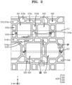
- FIG. 2 is a plan view schematically illustrating a part of the display apparatus of FIG. 1 .
- FIG. 3 is a cross-sectional view schematically illustrating the display apparatus of FIG. 2 taken along the line II-II' of FIG. 2 .
- FIG. 1 may schematically illustrate the display apparatus of claim 2 taken along the line I-I' of FIG. 2 .
- the display apparatus includes a second substrate 100 (lower substrate), and a first pixel electrode 311, a second pixel electrode 321, and a third pixel electrode 331 located on the second substrate 100, a pixel-defining film 150, a first substrate 400 (upper substrate), and a bank 500.
- the second substrate 100 may include glass, a metal, or a polymer resin.
- the second substrate 100 may include a polymer resin such as polyethersulfone, polyacrylate, polyetherimide, polyethylene naphthalate, polyethylene terephthalate, polyphenylene sulfide, polyarylate, polyimide, polycarbonate, or cellulose acetate propionate.
- a polymer resin such as polyethersulfone, polyacrylate, polyetherimide, polyethylene naphthalate, polyethylene terephthalate, polyphenylene sulfide, polyarylate, polyimide, polycarbonate, or cellulose acetate propionate.
- the second substrate 100 may have a multi-layer structure including two layers each including a polymer resin and a barrier layer including an inorganic material (e.g., silicon oxide, silicon nitride, or silicon oxynitride) and located between the two layers.
- the first pixel electrode 311, the second pixel electrode 321, and the third pixel electrode 331 are located on the second substrate 100.
- a first thin-film transistor 210, a second thin-film transistor 220, and a third thin-film transistor 230 respectively electrically connected to the first pixel electrode 311, the second pixel electrode 321, and the third pixel electrode 331 may be located on the second substrate 100. That is, as shown in FIGS.
- the first pixel electrode 311 may be electrically connected to the first thin-film transistor 210
- the second pixel electrode 321 may be electrically connected to the second thin-film transistor 220
- the third pixel electrode 331 may be electrically connected to the third thin-film transistor 230.
- the first pixel electrode 311, the second pixel electrode 321, and the third pixel electrode 331 may be located on a planarization layer 140 located on the second substrate 100.
- a buffer layer 110 including an inorganic material such as silicon oxide, silicon nitride, and/or silicon oxynitride may be located between the second substrate 100, and the first transistor 210, the second thin-film transistor 220, and the third thin-film transistor 230.
- the buffer layer 110 may planarize a top surface of the second substrate 100, or may prevent, reduce, or minimize impurities from the second substrate 100 or the like from penetrating into a first semiconductor layer 211 of the first thin-film transistor 210.
- the first thin-film transistor 210 that drives a first pixel PX1 may include the first semiconductor layer 211 including amorphous silicon, polycrystalline silicon, an organic semiconductor material, or an oxide semiconductor material, a first gate electrode 213, a first source electrode 215a, and a first drain electrode 215b.
- the first gate electrode 213 may include any of various conductive materials and may have any of various layer structures.
- the first gate electrode 213 may include a molybdenum (Mo) layer and an aluminum (Al) layer. In this case, the first gate electrode 213 may have a layer structure including Mo/Al/Mo. Alternatively, the first gate electrode 213 may include a TiNx layer, an aluminum (Al) layer, and/or a titanium (Ti) layer.
- Each of the first source electrode 215a and the first drain electrode 215b may also have any of various conductive materials and may have any of various layer structures.
- each of the first source electrode 215a and the first drain electrode 215b may include a Ti layer, an Al layer, and/or a copper (Cu) layer. In this case, each of the first source electrode 215a and the first drain electrode 215b may have a layer structure including Ti/Al/Ti.
- a gate insulating film 121 including an inorganic material such as silicon oxide, silicon nitride, and/or silicon oxynitride may be located between the first semiconductor layer 211 and the first gate electrode 213.
- An interlayer insulating film 131 including an inorganic material such as silicon oxide, silicon nitride, and/or silicon oxynitride may be located on the first gate electrode 213, and the first source electrode 215a and the first drain electrode 215b may be located on the interlayer insulating film 131.
- Such an insulating film including an inorganic material may be formed by using chemical vapor deposition (CVD) or atomic layer deposition (ALD). This applies to the following embodiments and modifications thereof.
- the second thin-film transistor 220 that drives a second pixel PX2 may include a second semiconductor layer 221, a second gate electrode 223, a second source electrode 225a, and a second drain electrode 225b.
- the third thin-film transistor 230 that drives a third pixel PX3 may include a third semiconductor layer 231, a third gate electrode 233, a third source electrode 235a, and a third drain electrode 235b.
- a structure of the second thin-film transistor 220 and a structure of the third thin-film transistor 230 are the same as or similar to a structure of the first thin-film transistor 210 that drives the first pixel PX1, and thus, a description thereof will be omitted.
- the planarization layer 140 may be located on the first thin-film transistor 210, the second thin-film transistor 220, and the third thin-film transistor 230.
- the planarization layer 140 may substantially planarize a top surface of a protective film that covers the first thin-film transistor 210.
- the planarization layer 140 may include an organic material such as acryl, benzocyclobutene (BCB), or hexamethyldisiloxane (HMDSO).
- the planarization layer 140 has a single-layer structure in FIGS. 1 and 3 , various modifications may be made.
- the planarization layer 140 may have a multi-layer structure.
- the organic light-emitting device including the first pixel electrode 311, a counter electrode 305, and an intermediate layer 303 located between the first pixel electrode 311 and the counter electrode 305 and including an emission layer may be located to correspond to the first pixel PX1.
- the first pixel electrode 311 is electrically connected to the first thin-film transistor 210 by contacting any one of the first source electrode 215a and the first drain electrode 215b through a contact hole formed in the planarization layer 140 as shown in FIG. 1 .
- the first pixel electrode 311 includes a light-transmitting conductive layer formed of a light-transmitting conductive oxide such as ITO, In 2 O 3 , or IZO, and a reflective layer formed of a metal such as Al or Ag.
- the first pixel electrode 311 may have a three-layer structure including ITO/Ag/ITO.
- an organic light-emitting device including the second pixel electrode 321, the counter electrode 305, and the intermediate layer 303 located between the second pixel electrode 321 and the counter electrode 305 and including an emission layer may be located to correspond to the second pixel PX2.
- An organic light-emitting device including the third pixel electrode 331, the counter electrode 305, and the intermediate layer 303 located between the third pixel electrode 331 and the counter electrode 305 and including an emission layer may be located to correspond to the third pixel PX3.
- the second pixel electrode 321 is electrically connected to the second thin-film transistor 220 by contacting any one of the second source electrode 225a and the second drain electrode 225b through a contact hole formed in the planarization layer 140.
- the third pixel electrode 331 is electrically connected to the third thin-film transistor 230 by contacting any one of the third source electrode 235a and the third drain electrode 235b through a contact hole formed in the planarization layer 140.
- the description of the first pixel electrode 311 may be applied to the second pixel electrode 321 and the third pixel electrode 331.
- the intermediate layer 303 including the emission layer may be located on the first pixel electrode 311 of the first pixel PX1, the second pixel electrode 321 of the second pixel PX2, and the third pixel electrode 331 of the third pixel PX3.
- the intermediate layer 303 may be integrally formed over the first pixel electrode 311, the second pixel electrode 321, and the third pixel electrode 331.
- the intermediate layer 303 may be patterned and located on the first pixel electrode 311, the second pixel electrode 321, and the third pixel electrode 331.
- the intermediate layer 303 may include a hole injection layer, a hole transport layer, and/or an electron transport layer when necessary in addition to the emission layer.
- Some of the layers included in the intermediate layer 303 may be integrally formed over the first pixel electrode 311 through the third pixel electrode 331, and other layers may be patterned and located on the first pixel electrode 311, the second pixel electrode 321, and the third pixel electrode 331.
- the counter electrode 305 on the intermediate layer 303 may be integrally formed over the first pixel electrode 311 through the third pixel electrode 331, like the intermediate layer 303.
- the counter electrode 305 may include a light-transmitting conductive layer formed of ITO, In 2 O 3 , or IZO, and may include a semi-transmissive film including a metal such as aluminum (Al), lithium (Li), magnesium (Mg), ytterbium (Yb), or silver (Ag).
- the counter electrode 305 may include a semi-transmissive film including MgAg, AgYb, Yb/MgAg, or Li/MgAg.
- the pixel-defining film 150 may be located on the planarization layer 140.
- the pixel-defining film 150 has an opening corresponding to each pixel. That is, the pixel-defining film 150 covers an edge of each of the first pixel electrode 311, the second pixel electrode 321, and the third pixel electrode 331, and has an opening through which a central portion of the first pixel electrode 311 is exposed, an opening through which a central portion of the second pixel electrode 321 is exposed, and an opening through which a central portion of the third pixel electrode 331 is exposed.
- the pixel-defining film 150 may define a pixel. Also, as shown in FIG.
- the pixel-defining film 150 may increase a distance between the counter electrode 305, and an edge of each of the first pixel electrode 311, the second pixel electrode 321, and the third pixel electrode 331, to prevent or reduce instances of an arc or the like occurring on the edge of each of the first pixel electrode 311, the second pixel electrode 321, and the third pixel electrode 331.
- the pixel-defining film 150 may include an organic material such as polyimide or hexamethyldisiloxane (HMDSO).
- the emission layer included in the intermediate layer 303 may emit light having a wavelength in a first wavelength band.
- the first wavelength band may range from 450 nm to 495 nm.
- the first substrate 400 is located over the second substrate 100, with the first pixel electrode 311, the second pixel electrode 321, and the third pixel electrode 331 therebetween.
- the first substrate 400 may include glass or a polymer resin.
- the first substrate 400 may include a polymer resin such as polyethersulfone, polyacrylate, polyetherimide, polyethylene naphthalate, polyethylene terephthalate, polyphenylene sulfide, polyarylate, polyimide, polycarbonate, or cellulose acetate propionate.
- a polymer resin such as polyethersulfone, polyacrylate, polyetherimide, polyethylene naphthalate, polyethylene terephthalate, polyphenylene sulfide, polyarylate, polyimide, polycarbonate, or cellulose acetate propionate.
- the first substrate 400 may have a multi-layer structure including two layers each including a polymer resin and a barrier layer including an inorganic material (e.g., silicon oxide, silicon nitride, or silicon oxynitride) and located between the two layers.
- the first substrate 400 may be flexible or bendable.
- the bank 500 is located on a bottom surface 400b of the first substrate 400 in a direction (-z direction) toward the second substrate 100. That is, the bank 500 is located between the first substrate 400 and the second substrate 100.
- the bank 500 includes first wells 501, second wells 502, third wells 503, fourth wells 504, and auxiliary wells AOP. According to some embodiments, the first wells 501, the second wells 502, the third wells 503, the fourth wells 504, and the auxiliary wells AOP may pass through the bank 500 and thus may be also called through-holes.
- widths d aw and d w of partition walls defining the first wells 501, the second wells 502, the third wells 503, the fourth wells 504, and the auxiliary wells AOP may be the same as or similar to one another.
- the first well 501 of the bank 500 is located to correspond to the opening of the pixel-defining film 150 through which the first pixel electrode 311 is exposed
- the second well 502 of the bank 500 is located to correspond to the opening of the pixel-defining film 150 through which the second pixel electrode 321 is exposed
- the third well 503 of the bank 500 is located to correspond to the opening of the pixel-defining film 150 through which the third pixel electrode 331 is exposed.
- the first well 501 of the bank 500 overlaps the opening of the pixel-defining film 150 through which the first pixel electrode 311 is exposed
- the second well 502 of the bank 500 overlaps the opening of the pixel-defining film 150 through which the second pixel electrode 321 is exposed
- the third well 503 of the bank 500 overlaps the opening of the pixel-defining film 150 through which the third pixel electrode 331 is exposed.
- a shape of an edge of each of the first well 501 through the third well 503 of the bank 500 may be the same as or similar to that of an edge of the corresponding opening of the pixel-defining film 150. Accordingly, the first well 501 of the bank 500 may be located to correspond to the first pixel electrode 311, the second well 502 of the bank 500 may be located to correspond to the second pixel electrode 321, and the third well 503 of the bank 500 may be located to correspond to the third pixel electrode 331.
- the bank 500 may be formed of any of various materials, and may include an inorganic material such as silicon oxide, silicon nitride, and/or silicon oxynitride. When necessary, the bank 500 may include a photoresist material, and in this case, the bank 500 may be easily formed through a process such as exposure and development.
- an inorganic material such as silicon oxide, silicon nitride, and/or silicon oxynitride.
- the bank 500 may include a photoresist material, and in this case, the bank 500 may be easily formed through a process such as exposure and development.
- a first quantum dot layer 415 may be located in the first wells 501 of the bank 500.
- the first quantum dot layer 415 may overlap the first pixel electrode 311 when viewed in the direction (z axis direction) perpendicular to the top surface 400a of the first substrate 400.
- the first quantum dot layer 415 may convert light having a wavelength in the first wavelength passing through the first quantum dot layer 415 into light having a wavelength in a second wavelength.
- the second wavelength band may range from, for example, about 630 nm to about 780 nm.
- the disclosure is not limited thereto, and a wavelength to which a wavelength converted by the first quantum dot layer 415 belongs and a wavelength band to which a wavelength after conversion belongs may be modified differently.
- the first quantum dot layer 415 may be formed so that quantum dots are dispersed in a resin.
- quantum dots may refer to semiconductor compound crystals, and may include any material capable of emitting light having various wavelengths according to sizes of crystals.
- a diameter of each of the quantum dots may range, for example, from about 1 nm to about 10 nm.
- Quantum dots may be synthesized by using a wet chemical process, metal organic chemical deposition, molecular beam epitaxy, or the like.
- a wet chemical process is a method of mixing an organic solvent with a precursor material and then growing quantum dot crystals.
- the wet chemical process when crystals are grown, because an organic solvent naturally functions as a dispersant coordinated on quantum dot crystal surfaces and controls the growth of the crystals, the wet chemical process is easier than a vapor deposition method such as organic metal chemical vapor deposition (MOCVD) or molecular beam epitaxy (MBE).
- MOCVD organic metal chemical vapor deposition
- MBE molecular beam epitaxy
- the wet chemical process is inexpensive and may control the growth of quantum dot particles.
- Such quantum dots may include a group III-VI semiconductor compound, a group II-VI semiconductor compound, a group III-V semiconductor compound, a group I-III-VI semiconductor compound, a group IV-VI semiconductor compound, a group IV element or compound, or any combination thereof.
- Examples of the group III-VI semiconductor compound may include a binary compound such as GaS, GaSe, Ga 2 Se 3 , GaTe, InS, InSe, In 2 Se 3 , or InTe, a ternary compound such as InGaS 3 or InGaSe 3 , and any combination thereof.
- Examples of the group II-VI semiconductor compound may include a binary compound such as CdS, CdSe, CdTe, ZnS, ZnSe, ZnTe, ZnO, HgS, HgSe, HgTe, MgSe, or MgS, a ternary compound such as CdSeS, CdSeTe, CdSTe, ZnSeS, ZnSeTe, ZnSTe, HgSeS, HgSeTe, HgSTe, CdZnS, CdZnSe, CdZnTe, CdHgS, CdHgSe, CdHgTe, HgZnS, HgZnSe, HgZnTe, MgZnSe, or MgZnS, a quaternary compound such as CdZnSeS, CdZnSeTe, CdZnSTe, CdHgSeS, CdHg
- Examples of the group III-V semiconductor compound may include a binary compound such as GaN, GaP, GaAs, GaSb, AlN, AlP, AlAs, AlSb, InN, InP, InAs, or InSb, a ternary compound such as GaNP, GaNAs, GaNSb, GaPAs, GaPSb, AlNP, AlNAs, AlNSb, AlPAs, AlPSb, InGaP, InNP, InAlP, InNAs, InNSb, InPAs, InPSb, or GaAlNP, a quaternary compound such as GaAlNAs, GaAlNSb, GaAlPAs, GaAlPSb, GaInNP, GaInNAs, GaInNSb, GaInPAs, GaInPSb, InAlNP, InAlNAs, InAlNSb, InAlPAs, or InAlPSb, and any combination thereof.
- the group III-V semiconductor compound may further include a group II element. Examples of the
- Examples of the group I-III-VI semiconductor compound may include a ternary compound such as AgInS, AgInS 2 , CuInS, CuInS 2 , CuGaO 2 , AgGaO 2 , or AgAlO 2 , and any combination thereof.
- Examples of the group IV-VI semiconductor compound may include a binary compound such as SnS, SnSe, SnTe, PbS, PbSe, or PbTe, a ternary compound such as SnSeS, SnSeTe, SnSTe, PbSeS, PbSeTe, PbSTe, SnPbS, SnPbSe, or SnPbTe, a quaternary compound such as SnPbSSe, SnPbSeTe, or SnPbSTe, and any combination thereof.
- Examples of the group IV element or compound may include a single-element compound such as Si or Ge, a binary compound such as SiC or SiGe, and any combination thereof.
- Elements included in a multi-element compound such as a binary compound, a ternary compound, or a quaternary compound may exist in particles at a uniform concentration or a non-uniform concentration.
- a quantum dot may have a core-shell structure or a single structure having a uniform element concentration in the quantum dot.
- a material included in a core and a material included in a shell may be different from each other.
- the shell of the quantum dot may serve as a protective layer for maintaining semiconductor characteristics by preventing or reducing chemical degeneration of the core and/or a charging layer for providing electrophoretic characteristics to the quantum dot.
- the shell may have a single or multi-layer structure.
- An interface between the core and the shell may have a concentration gradient in which a concentration of an element in the shell gradually decreases toward the center.
- Examples of the shell of the quantum dot may include a metallic or non-metallic oxide, a semiconductor compound, and a combination thereof.
- Examples of the metallic or non-metallic oxide may include a binary compound such as SiO 2 , Al 2 O 3 , TiO 2 , ZnO, MnO, Mn 2 O 3 , Mn 3 O 4 , CuO, FeO, Fe 2 O 3 , Fe 3 O 4 , CoO, Co 3 O 4, , or NiO, a ternary compound such as MgAl 2 O 4 , CoFe 2 O 4 , NiFe 2 O 4 , or CoMn 2 O 4 , and any combination thereof.
- Examples of the semiconductor compound may include, as described above, a group III-VI semiconductor compound, a group II-VI semiconductor compound, a group III-V semiconductor compound, a group I-III-VI semiconductor compound, a group IV-VI semiconductor compound, and any combination thereof.
- Examples of the semiconductor compound may include CdS, CdSe, CdTe, ZnS, ZnSe, ZnTe, ZnSeS, ZnTeS, GaAs, GaP, GaSb, HgS, HgSe, HgTe, InAs, InP, InGaP, InSb, AlAs, AlP, AlSb, and any combination thereof.
- a quantum dot may have a full width at half maximum (FWHM) of an emission wavelength spectrum of about 45 nm or less, specifically about 40 nm or less, and more specifically about 30 nm or less.
- FWHM full width at half maximum
- color purity or color reproducibility may be improved.
- an optical viewing angle may be improved.
- a quantum dot may be a spherical, pyramid, multi-arm, or cubic-shaped nano particle, nano-tube, nano-wire, nano-fiber, or nano-plate particle.
- an energy band gap may be adjusted by adjusting a size of a quantum dot
- light of various wavelength bands may be obtained through a quantum dot emission layer.
- a light-emitting device for emitting light having various wavelengths may be realized by using quantum dots having different sizes.
- a size of a quantum dot may be selected to emit red light, green light, and/or blue light.
- a size of a quantum dot may be selected to emit white light by combining light of various colors.
- the first quantum dot layer 415 may include a scatterer. Because incident light is scattered by the scatterer included in the first quantum dot layer 415, the incident light may be efficiently converted by the quantum dots in the first quantum dot layer 415.
- the scatterer is not particularly limited as long as it is capable of partially scattering transmitted light by forming an optical interface between the scatterer and a light-transmitting resin.
- the scatterer may be metal oxide particles or organic particles.
- Examples of a metal oxide for the scatterer may include titanium oxide (TiO 2 ), zirconium oxide (ZrO 2 ), aluminum oxide (Al 2 O 3 ), indium oxide (In 2 O 3 ), zinc oxide (ZnO), and tin oxide (SnO 2 ), and examples of an organic material for the scatterer may include an acrylic resin and a urethane resin.
- the scatterer may scatter light in several directions regardless of an angle of incidence without substantially converting a wavelength of incident light. Accordingly, the scatterer may improve side visibility of the display apparatus. Also, the scatterer included in the first quantum dot layer 415 may increase the probability that light incident on the first quantum dot layer 415 meets the quantum dots, thereby improving light conversion efficiency.
- the resin included in the first quantum dot layer 415 may be any resin as long as it has excellent scattering characteristics for the scatterer and is a light-transmitting material.
- a polymer resin such as acrylic resin, an imide-based resin, an epoxy resin, benzocyclobutene (BCB), or hexamethyldisiloxane (HMDSO) may be used as a material for forming the first quantum dot layer 415.
- the material for forming the first quantum dot layer 415 may be located in the first well 501 of the bank 500 overlapping the first pixel electrode 311, through inkjet printing.
- a second quantum dot layer 425 may be located in the second wells 502 of the bank 500.
- the second quantum dot layer 425 may overlap the second pixel electrode 321 when viewed in the direction (z axis direction) perpendicular to the top surface 400a of the first substrate 400.
- the second quantum dot layer 425 may convert light having a wavelength in the first wavelength band passing through the second quantum dot layer 425 into light having a wavelength in a third wavelength band.
- the third wavelength band may range from, for example, about 495 nm to about 570 nm.
- the disclosure is not limited thereto, and a wavelength band to which a wavelength converted by the second quantum dot layer 425 belongs and a wavelength band to which a wavelength after conversion belongs may be modified differently.
- the second quantum dot layer 425 may be formed so that quantum dots are dispersed in a resin.
- quantum dots may refer to semiconductor compound crystals, and may include any material capable of emitting light having various wavelengths according to sizes of crystals.
- a diameter of each of the quantum dots may range from, for example, about 1 nm to about 10 nm.
- the description of the quantum dots included in the first quantum dot layer 415 may be applied to the quantum dots included in the second quantum dot layer 425, and thus, a description of the quantum dots included in the second quantum dot layer 425 will be omitted.
- the second quantum dot layer 425 may include a scatterer. Because incident light is scattered by the scatterer included in the second quantum dot layer 425, the incident light may be efficiently converted by the quantum dots in the second quantum dot layer 425.
- the scatterer is not particularly limited as long as it is capable of partially scattering transmitted light by forming an optical interface between the scatterer and a light-transmitting resin.
- the scatterer may be metal oxide particles or organic particles. A metal oxide for the scatterer or an organic material for the scatterer are the same as described above.
- the scatterer may scatter light in several directions regardless of an angle of incidence without substantially converting a wavelength of incident light. Accordingly, the scatterer may improve side visibility of the display apparatus.
- the scatterer included in the second quantum dot layer 425 may increase the probability that light incident on the second quantum dot layer 425 meets the quantum dots, thereby improving light conversion efficiency.
- the resin included in the second quantum dot layer 425 may be any resin as long as it has excellent distribution characteristics for the scatterer and is a light-transmitting material.
- a polymer resin such as an acrylic resin, an imide-based resin, an epoxy resin, BCB, or HMDSO may be used as a material for forming the second quantum dot layer 425.
- the material for forming the second quantum dot layer 425 may be located in the second well 502 of the bank 500 overlapping the second pixel electrode 321, through inkjet printing.
- the third pixel PX3 emits light having a wavelength in the first wavelength band generated by the intermediate layer 303 including the emission layer to the outside through the first substrate 400 without wavelength conversion. Accordingly, the third pixel PX3 does not include a quantum dot layer.
- a light-transmitting layer 435 including a light-transmitting resin may be located in the third well 503 of the bank 500 overlapping the third pixel electrode 331.
- the light-transmitting layer 435 may include acryl, BCB, or HMDSO.
- the light-transmitting layer 435 may include a scatterer. When necessary, unlike in FIG. 1 , the light-transmitting layer 435 may not be located in the third well 503 of the bank 500.
- the first quantum dot layer 415 and the second quantum dot layer 425 may be formed by using inkjet printing. That is, after the bank 500 including the first well 501, the second well 502, and the third well 503 is formed on the first substrate 400, the first quantum dot layer 415 and the second quantum dot layer 425 may be formed by dotting the material for forming the first quantum dot layer 415 in the first well 501 by using inkjet printing and dotting the material for forming the second quantum dot layer 425 in the second well 502 by using inkjet printing.
- the display apparatus in order to reduce the probability that the material for forming the first quantum dot layer 415 is located in the second well 502 or the third well 503 and the probability that the material for forming the second quantum dot layer 425 is located in the first well 501 or the third well 503, the display apparatus according to some embodiments includes the auxiliary wells AOP surrounding the first well 501, the second well 502, the third well 503, and the fourth well 504 in the bank 500 as shown in FIGS. 1 through 3 .
- the material for forming the first quantum dot layer 415 when the material for forming the first quantum dot layer 415 is dotted by using inkjet printing, even if the material is not located in the first well 501, the material may be located in the auxiliary well AOP, thereby reducing the probability that the material is located in the second well 502 or the third well 503. Also, when the material for forming the second quantum dot layer 425 is dotted by using inkjet printing, even if the material is not located in the second well 502, the material may be located in the auxiliary well AOP, thereby reducing the probability that the material is located in the first well 501 or the third well 503.
- the auxiliary wells AOP may include first auxiliary wells 510 adjacent to the first well 501, second auxiliary wells 520 adjacent to the second well 502, third auxiliary wells 530 adjacent to the third well 503, and fourth auxiliary wells 540 adjacent to the fourth well 504, as shown in FIG. 2 .
- a and B when A and B are adjacent to each other, it means that a part of a partition wall defining A is a part of a partition wall defining B. In other words, A and B share the same partition wall. Accordingly, when a partition wall shared by A and B is lost, a material located in A may flow out to B, or a material located in B may flow out to A.
- One auxiliary well AOP may be included in at least one of the first auxiliary wells 510, the second auxiliary wells 520, the third auxiliary wells 530, or the fourth auxiliary wells 540.
- the first auxiliary wells 510 adjacent to the first well 501 include 1-1 th through 1-10 th auxiliary wells 510a, ..., and 510j.
- the 1-4 th auxiliary well 510d and the 1-5 th auxiliary well 510e are located between the first well 501 and the third well 503, and the 1-4 th auxiliary well 510d and the 1-5 th auxiliary well 510e are adjacent to the first well 501 and the third well 503.
- the 1-4 th auxiliary well 510d and the 1-5 th auxiliary well 510e may be included in both the first auxiliary wells 510 and the third auxiliary wells 530.
- the 1-6 th auxiliary well 510f is located between the first well 501 and the second well 502, and the 1-6 th auxiliary well 510f is adjacent to the first well 501 and the second well 502. Accordingly, the 1-6 th auxiliary well 510f may be included in the first auxiliary wells 510 and may be included in the second auxiliary wells 520.
- An area of each of the first auxiliary wells 510 adjacent to the first well 501 may be proportional to an area of the first well 501.
- an area of each of the first auxiliary wells 510 may be equal to or less than about 27% of an area of the first well 501.
- the first pixel PX1 when the first pixel PX1 emits red light, even if a part of a partition wall defining the first well 501 is lost and a material for forming the first quantum dot layer 415 leaks to the first auxiliary well 510, visibility of a change in a luminance of the corresponding pixel may be prevented or reduced.
- an area of each of the first auxiliary wells 510 may be equal to or less than about 23% of an area of the first well 501.
- the first quantum dot layer 415 may be formed to have a sufficient thickness (e.g., a height in the z direction). For reference, a thickness of the first quantum dot layer 415 may be 9 ⁇ m.
- an area of each of the first auxiliary wells 510 is equal to or less than 23% of an area of the first well 501, even when a part of a partition wall defining the first well 501 is lost, a thickness of the first quantum dot layer 415 may be prevented from being reduced by 2 ⁇ m or more.
- an area of each of the second auxiliary wells 520 adjacent to the second well 502 may be proportional to an area of the second well 502.
- an area of each of the second auxiliary wells 520 may be equal to or less than about 45% of an area of the second well 502.
- the second pixel PX2 when the second pixel PX2 emits green light, even if a part of a partition wall defining the second well 502 is lost and a material for forming the second quantum dot layer 425 leaks to the second auxiliary well 520, visibility of a change in a luminance of the corresponding pixel may be prevented or reduced.
- an area of each of the second auxiliary wells 520 may be equal to or less than about 23% of an area of the second well 502.
- an area of each of the second auxiliary wells 520 is equal to or less than about 23% of an area of the second well 502
- the second quantum dot layer 425 may be formed to have a sufficient thickness (e.g., a height in the z direction).
- the light-transmitting layer 435 is located in the third well 503 as described above. Even when a part of a partition wall defining the third well 503 is lost and a material for forming the light-transmitting layer 435 dotted by using inkjet printing in a manufacturing process leaks to the outside of the third well 503, there may not be a large change in the amount of light emitted by the third pixel PX3 after the manufacturing process. However, because the light-transmitting layer 435 includes a scatterer or the like, it may be desirable to minimize the amount of leakage of a material for forming the light-transmitting layer 435.
- an area of each of the third auxiliary wells 530 adjacent to the third well 503 may be proportional to an area of the third well 503.
- an area of each of the third auxiliary well 530 may be equal to or less than about 77% of an area of the third well 503.
- an area of each of the third auxiliary wells 530 may be equal to or less than about 23% of an area of the third well 503.
- an area of each of the third auxiliary well 530 is equal to or less than about 23% of an area of the third well 503, even when a part of a partition wall defining the third well 503 is lost and a material for forming the light-transmitting layer 435 located in the third well 503 leaks to the third auxiliary well 530, the light-transmitting layer 435 may be formed to have a sufficient thickness (e.g., a height in the z direction).
- the fourth well 504 does not correspond to the first pixel PX1, the second pixel PX2, and the third pixel PX3. That is, the fourth well 504 does not overlap the first pixel electrode 311, the second pixel electrode 321, and the third pixel electrode 331. Accordingly, the first quantum dot layer 415, the second quantum dot layer 425, and the light-transmitting layer 435 may not be located in the fourth well 504. Even when there is no material in the fourth well 504, the fourth auxiliary wells 540 are located between the fourth well 504, and the first well 501, the second well 502, and the third well 503.
- a material for forming the first quantum dot layer 415, a material for forming the second quantum dot layer 425, or a material for forming the light-transmitting layer 435 may leak to the fourth well 504, and thus, visibility of a change in a luminance of a corresponding pixel may be prevented or reduced.
- one auxiliary well AOP may be included in at least one of the first auxiliary wells 510, the second auxiliary wells 520, the third auxiliary wells 530, or the fourth auxiliary wells 540.
- the 1-4 th auxiliary well 510d is adjacent to the first well 501 and the third well 503, and is included in the first auxiliary wells 510 and is included in the third auxiliary wells 530.
- an area of the 1-4 th auxiliary well 510d may be equal to or less than a smaller area from among about 27% or less of an area of the first well 501 and about 77% or less of an area of the third well 503.
- an area of the 1-4 th auxiliary well 510d may be equal to or less than a smaller area from among about 23% or less of an area of the first well 501 and about 77% or less of an area of the third well 503. According to some embodiments, an area of the 1-4 th auxiliary well 510d may be equal to or less than a smaller area from among about 27% or less of an area of the first well 501 and about 23% or less of an area of the third well 503. According to some embodiments, an area of the 1-4 th auxiliary well 510d may be equal to or less than a smaller area from among about 23% or less of an area of the first well 501 and about 23% or less of an area of the third well 503.
- the 1-7 th auxiliary well 510g is adjacent to the first well 501, the second well 502, and the third well 503, and is included in the first auxiliary wells 510, the second auxiliary wells 520, and the third auxiliary wells 530.
- an area of the 1-7 th auxiliary well 510g may be equal to or less than a smallest area from among about 27% or less of an area of the first well 501, about 45% or less of an area of the second well 502, and about 77% or less of an area of the third well 503.
- an area of the 1-7 th auxiliary well 510g may be equal to or less than a smallest area from among about 23% or less of an area of the first well 501, about 45% or less of an area of the second well 502, and about 77% or less of an area of the third well 503.
- an area of the 1-7 th auxiliary well 510g may be equal to or less than a smallest area from among about 27% or less of an area of the first well 501, about 23% or less of an area of the second well 502, and about 77% or less of an area of the third well 503.
- an area of the 1-7 th auxiliary well 510g may be equal to or less than a smallest area from among about 27% or less of an area of the first well 501, about 45% or less of an area of the second well 502, and about 23% or less of an area of the third well 503. According to some embodiments, an area of the 1-7 th auxiliary well 510g may be equal to or less than a smallest area from among about 23% or less of an area of the first well 501, about 23% or less of an area of the second well 502, and about 77% or less of an area of the third well 503.
- an area of the 1-7 th auxiliary well 510g may be equal to or less than a smallest area from among about 23% or less of an area of the first well 501, about 45% or less of an area of the second well 502, and about 23% or less of an area of the third well 503. According to some embodiments, an area of the 1-7 th auxiliary well 510g may be equal to or less than a smallest area from among about 27% or less of an area of the first well 501, about 23% or less of an area of the second well 502, and about 23% or less of an area of the third well 503.
- an area of the 1-7 th auxiliary well 510g may be equal to or less than a smallest area from among about 23% or less of an area of the first well 501, about 23% or less of an area of the second well 502, and about 23% or less of an area of the third well 503. Accordingly, an area of any one of the auxiliary wells AOP may be equal to or less than an area of another one of the auxiliary wells AOP.
- auxiliary wells 510a, ..., and 510j are included in the first auxiliary well 510 in FIG. 2
- the disclosure is not limited thereto.
- the number of auxiliary wells AOP included in the first auxiliary wells 510 may change as long as the above area-related rules are satisfied and the first well 501 is surrounded.
- the 1-4 th auxiliary well 510d and the 1-5 th auxiliary well 510e are located between the first well 501 and the third well 503 in FIG. 2
- three auxiliary wells AOP may be located between the first well 501 and the third well 503.
- second auxiliary wells 520, third auxiliary wells 530, and fourth auxiliary wells 540 may change as long as the second well 502, the third well 503, and the fourth well 504 are surrounded and the above area-related rules are satisfied.
- Widths d aw and d w of partition walls defining the first well 501, the second well 502, the third well 503, the fourth well 504, and the auxiliary well AOP may be equal or similar to one another.
- a width d w of a partition wall shared by the second well 502 and the 1-6 th auxiliary well 510f and a width d aw of a partition wall shared by the 1-6 th auxiliary well 510f and the 1-7 th auxiliary well 510g may be equal or similar to each other.
- each of the widths d aw and d w of the partition walls may range from about 13 ⁇ m to about 15 ⁇ m.
- the widths d aw and d w of the partition walls defining the first well 501, the second well 502, the third well 503, the fourth well 504, and the auxiliary well AOP are sufficiently large, parts of the partition walls defining the first well 501, the second well 502, the third well 503, the fourth well 504, and the auxiliary well AOP may be prevented from being lost.
- the first well 501, the second well 502, the third well 503, and the fourth well 504 of the bank 500 may be located on a plurality of imaginary lines, and the auxiliary wells AOP of the bank 500 may be located between the first well 501, the second well 502, the third well 503, and the fourth well 504.
- FIG. 1 In this regard, in FIG. 1
- the first well 501 and the third well 503 are located on a first imaginary line IL1 extending in a first direction (e.g., x direction)
- the second well 502 and the fourth well 504 extend in the first direction (e.g., x direction) and are located on a second imaginary line IL2 that is spaced apart from the first imaginary line IL1 in a second direction (e.g., y direction)
- the auxiliary wells AOP are located between the first well 501, the second well 502, the third well 503, and the fourth well 504 that are spaced apart from one another.
- the first well 501 and the third well 503 may be alternately arranged on the first imaginary line IL1
- the second well 502 and the fourth well 504 may be alternately arranged on the second imaginary line IL2.
- the center of the first well 501 and the center of the third well 503 located on the first imaginary line IL1 from among a plurality of lines may correspond to between the center of the second well 502 and the center of the fourth well 504 located on the second imaginary line IL2 closest to the first imaginary line IL1 from among the plurality of lines. That is, the auxiliary wells AOP located between the first well 501 and the third well 503 may substantially correspond to the center of the second well 502 or the center of the fourth well 504. Likewise, the auxiliary wells AOP located between the second well 502 and the fourth well 504 may substantially correspond to the center of the first well 501 or the third well 503. Accordingly, an overall structure of the bank 500 may be more robust.
- each of the first well 501, the second well 502, the third well 503, the fourth well 504, and the auxiliary wells AOP may have a polygonal shape.
- each of the first well 501, the second well 502, and the third well 503 may have a quadrangular shape with a chamfered corner, and the fourth well 504 may have an octagonal shape.
- Each of the auxiliary wells AOP may be located between the first well 501, the second well 502, the third well 503, and the fourth well 504, and may have any of various polygonal shapes as long as it satisfies the above area-related rules.
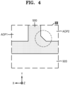
- FIG. 4 is an enlarged view of a portion III of FIG. 2 .
- a chamfered portion is marked by a dashed circle. Accordingly, a portion where a partition wall and a partition wall meet each other may be sufficiently thick and a sufficient area of the auxiliary well AOP may be ensured.
- a corner of a partition wall shared with the fourth well 504 may not be chamfered.
- FIG. 5 is an enlarged view of a portion IV of FIG. 2 .
- the fourth well 504 has an octagonal shape
- three partition walls meet at one point to form a first angle ⁇ 1, a second angle ⁇ 2, and a third angle ⁇ 3.
- the bank 500 may have sufficient structural stability.
- a color filter layer may be located between the bottom surface 400b of the first substrate 400 in a direction (e.g., -z direction) toward the second substrate 100, and the first quantum dot layer 415, the second quantum dot layer 425, and the light-transmitting layer 435. That is, a first color filter layer 410 may be located between the first substrate 400 and the first quantum dot layer 415, a second color filter layer 420 may be located between the first substrate 400 and the second quantum dot layer 425, and a third color filter layer 430 may be located between the first substrate 400 and the light-transmitting layer 435.
- the first color filter layer 410 may be a layer that passes only light having a wavelength ranging from 630 nm to 780 nm.
- the second color filter layer 420 may be a layer that passes only light having a wavelength ranging from 495 nm to 570 nm.
- the third color filter layer 430 may be a layer that passes only light having a wavelength ranging from 450 nm to 495 nm.
- the first color filter layer 410 through the third color filter layer 430 may increase the color purity of light emitted to the outside and may improve the quality of a displayed image. Also, because the first color filter layer 410 through the third color filter layer 430 reduces a ratio of light, from among external light incident from the outside on the display apparatus, reflected by the first pixel electrode 311 through the third pixel electrode 331 and then emitted to the outside again, the reflection of external light may be reduced. When necessary, a black matrix may be located between the first color filter layer 410 through the third color filter layer 430.
- the second color filter layer 420 and the third color filter layer 430 have an opening 421 through which a first area A1 is exposed as shown in FIG. 1 .
- the opening 421 may define an area of the first pixel PX1.
- the first color filter layer 410 fills at least the opening 421.
- the first color filter layer 410 and the second color filter layer 420 have an opening 423 through which a third area A3 is exposed.
- the opening 423 may define an area of the third pixel PX3.
- the first color filter layer 410 and the third color filter layer 430 have an opening 412 through which a second area A2 is exposed as shown in FIG. 3 .
- the opening 412 may define an area of the second pixel PX2.
- the second color filter layer 420 fills at least the opening 412.
- a portion where the first color filter layer 410 and the third color filter layer 430 overlap each other, a portion where the second color filter layer 420 and the third color filter layer 430 overlap each other, and a portion where the first color filter layer 410 and the second color filter layer 420 overlap each other may each function as a black matrix.
- the third color filter layer 430, the first color filter layer 410, and the second color filter layer 420 may be sequentially stacked on the first substrate 400 in the direction (e.g., -z direction) toward the second substrate 100.
- a protective layer 600 may be located on a surface of the first quantum dot layer 415, the second quantum dot layer 425, and the light-transmitting layer 435 in a direction toward the second substrate 100.
- the protective layer 600 may include an inorganic material such as silicon oxide or silicon nitride.
- the protective layer 600 may have a two-layer structure including a silicon oxide layer and a silicon nitride layer. When there is no material in the fourth well 504 and the auxiliary well AOP, the protective layer 600 may cover an inner surface and a bottom surface of each of the fourth well 504 and the auxiliary well AOP as shown in FIGS. 1 and 3 .
- a filler may fill a space between the first substrate 400 and the second substrate 100.
- the filler may fill a space between the protective layer 600 and the counter electrode 305.
- the filler may include a light-transmitting material.
- the filler may include an acrylic resin or an epoxy resin.
- FIG. 6 is a plan view schematically illustrating a part of a display apparatus, according to some embodiments.
- FIG. 7 is a cross-sectional view schematically illustrating the display apparatus of FIG. 6 taken along the line V-V' of FIG. 6 .
- the display apparatus may include a spacer 700 as shown in FIG. 7 to maintain a constant interval between the second substrate 100 and the first substrate 400.
- the bank 500 may include a support 500P for locating the spacer 700.
- the support 500P may overlap a fourth well 504' when viewed in a direction (e.g., z direction) perpendicular to a top surface of the first substrate 400.
- a direction e.g., z direction
- the fourth well 504' and auxiliary wells AOP' of some of the fourth auxiliary wells 540 overlap the support 500P.
- the fourth well 504' overlapping the support 500P may have a smaller area than other fourth wells 504 (see FIG. 2 ).
- the auxiliary wells AOP' overlapping the support 500P may have a smaller area than other corresponding auxiliary wells AOP.
- FIG. 8 is a cross-sectional view schematically illustrating a part of a display apparatus, according to some embodiments.
- FIG. 9 is a cross-sectional view schematically illustrating a part of the display apparatus of FIG. 8 .
- a low-refractive index layer 900 may be further provided between the bank 500, and the first quantum dot layer 415, the second quantum dot layer 425, and the light-transmitting layer 435, and between the first color filter layer 410, the second color filter layer 420, and the third color filter layer 430.
- An additional protective layer 800 is further provided between the low-refractive index layer 900, and the first quantum dot layer 415, the second quantum dot layer 425, the light-transmitting layer 435, and the bank 500.
- the low-refractive index layer 900 may include an organic material having a low refractive index, and may increase light extraction efficiency of light passing through the first quantum dot layer 415 and the second quantum dot layer 425 and extracted to the outside through the first substrate 400.
- the additional protective layer 800 may include silicon oxide or silicon nitride, and may protect, along with the protective layer 600, the first quantum dot layer 415 and the second quantum dot layer 425 by preventing or reducing penetration of external impurities into the first quantum dot layer 415 and the second quantum dot layer 425. When there is no material in the fourth well 504 or the auxiliary well AOP, the protective layer 600 may contact the additional protective layer 800 in the fourth well 504 and the auxiliary well AOP.
- FIGS. 10A , 10B , and 10C are graphs illustrating a change in a luminance of a pixel according to a ratio between an area of a well corresponding to each pixel electrode and an area of an auxiliary well connected when a partition wall is lost.
- FIGS. 10A , 10B , and 10C are views results obtained after measuring whether a change in a luminance of a pixel is visible with eyes when a part of a partition wall of a well (e.g., the first well, the second well, or the third well) corresponding to each pixel electrode is removed and a material for forming a quantum dot layer leaks to connected auxiliary wells.
- a part of a partition wall of a well e.g., the first well, the second well, or the third well
- a change in a luminance of a corresponding pixel was checked when a material for forming a first quantum dot layer leaks from the first well 501 to the 1-1 th auxiliary well 510a by removing a partition wall between the first well 501 (see FIG. 2 ) and the 1-1 th auxiliary well 510a (see FIG. 2 ), and a change in a luminance of a corresponding pixel was checked when a material for forming a first quantum dot layer leaks from the first well 501 to the 1-1 th auxiliary well 510a and the 1-2 th auxiliary well 510b by additionally removing a partition wall between the first well 501 and the 1-2th auxiliary well 510b (see FIG. 2 ).
- whether a change in a luminance of a corresponding pixel is visible with eyes was measured by increasing an area of an auxiliary well connected to a well by removing some partition walls of a bank.
- FIG. 10A is a graph illustrating a change in a luminance of a pixel that emits blue light.
- a change in a luminance of a pixel was observed by changing an area ratio of the third auxiliary wells 530 (see FIG. 2 ) connected to the third well 503 (see FIG. 2 ) by removing some partition walls of a bank.
- an area of the third auxiliary wells 530 connected to the third well 503 is equal to or less than 77% of an area of the third well 503
- a change in a luminance of the pixel that emits blue light was not visible with eyes, whereas when the area exceeds 77%, it was recognized that the pixel had a higher luminance than a normal pixel.
- a maximum area of one third auxiliary well 530 in which defects are not visible when a partition wall is lost and the third auxiliary well 530 is connected to the third well 503 is equal to or less than 77% of an area of the third well 503.
- FIG. 10B is a graph illustrating a change in a luminance of a pixel that emits green light.
- a change in a luminance of a pixel was observed by changing an area ratio of the second auxiliary wells 520 (see FIG. 2 ) connected to the second well 502 (see FIG. 2 ) by removing some partition walls of a bank.
- an area of the second auxiliary wells 520 connected to the second well 502 is equal to or less than 45% of an area of the second well 502
- a change in a luminance of the pixel that emits green light was not visible with eyes, whereas when the area exceeds 45%, it was recognized that the pixel had a lower luminance than a normal pixel.
- a maximum area of one second auxiliary well 520 in which defects are not visible when a partition wall is lost and the second auxiliary well 520 is connected to the second well 502 is equal to or less than 45% of an area of the second well 502.
- FIG. 10C is a graph illustrating a change in a luminance of a pixel that emits red light.
- a change in a luminance of a pixel was observed by changing an area ratio of the first auxiliary wells 510 (see FIG. 2 ) connected to the first well 501 (see FIG. 2 ) by removing some partition walls of a bank.
- an area of the first auxiliary wells 510 connected to the first well 501 is equal to or less than 27% of an area of the first well 501
- a change in a luminance of the pixel that emits red light was not visible with eyes, whereas when the area exceeds 27%, it was recognized that the pixel had a lower luminance than a normal pixel.
- a maximum area of one first auxiliary well 510 in which defects are not visible when a partition wall is lost and the first auxiliary well 510 is connected to the first well 501 is equal to or less than 27% of an area of the first well 501.
- a display apparatus having a relatively reduced risk of defects in a manufacturing process may be realized.
- the scope of embodiments according to the present disclosure are not limited by these characteristics.
Landscapes
- Engineering & Computer Science (AREA)
- Microelectronics & Electronic Packaging (AREA)
- Physics & Mathematics (AREA)
- Optics & Photonics (AREA)
- Electroluminescent Light Sources (AREA)
Abstract
Description
- The present invention relates to a display apparatus.
- A display apparatus includes a plurality of pixels. In order to enable a full-color display apparatus, each pixel may emit light of a different color. To this end, at least some pixels of the display apparatus include a color conversion unit. Accordingly, light having a wavelength in a first wavelength band generated by a light emitter of some pixels may be converted into light having a wavelength in a second wavelength band while passing through a corresponding color conversion unit and may be extracted to the outside.
- The above information disclosed in this Background section is only for enhancement of understanding of the background and therefore the information discussed in this Background section does not necessarily constitute prior art.
- The present invention relates to a display apparatus, and for example, to a display apparatus capable of reducing the risk of defects in a manufacturing process.
- A display apparatus may have a problem in that defects are likely to occur in a manufacturing process.
- Embodiments of the present invention include a display apparatus that may have a relatively reduced risk of defects in a manufacturing process. However, the detailed embodiments are examples, and do not limit the scope of the disclosure.
- A display apparatus according to the present invention comprises the features of
claim 1. The dependent claims describe preferred embodiments. Additional aspects will be set forth in part in the description which follows and, in part, will be apparent from the description, or may be learned by practice of the presented embodiments. - According to the present invention, a display apparatus includes a first substrate, a bank located on the first substrate and including a first well, a second well, a third well, a fourth well, and auxiliary wells, a first quantum dot layer located in the first well, and a second quantum dot layer located in the second well, wherein the first well, the second well, the third well, and the fourth well are spaced apart from one another with the auxiliary wells therebetween.
- According to some embodiments, the first quantum dot layer may be configured to convert light having a wavelength in a first wavelength band passing through the first quantum dot layer into light having a wavelength in a second wavelength band, and the second quantum dot layer may be configured to convert light having a wavelength in the first wavelength band passing through the second quantum dot layer into light having a wavelength in a third wavelength band.
- According to some embodiments, the second wavelength band may include a wavelength ranging from 630 nm to 780 nm, wherein the auxiliary wells include a first auxiliary well adjacent to the first well, and an area of the first auxiliary well is equal to or less than 27% of an area of the first well.
- According to some embodiments, the third wavelength band may include a wavelength ranging from 495 nm to 570 nm, wherein the auxiliary wells include a second auxiliary well adjacent to the second well, and an area of the second auxiliary well is equal to or less than 45% of an area of the second well.
- According to some embodiments, the display apparatus may further include a light-transmitting layer located in the third well and configured to transmit incident light, wherein the auxiliary wells include a third auxiliary well adjacent to the third well, and an area of the third auxiliary well is equal to or less than 77% of an area of the third well.
- According to some embodiments, the auxiliary wells may include a first auxiliary well adjacent to the first well, a second auxiliary well adjacent to the second well, and a third auxiliary well adjacent to the third well, wherein an area of the first auxiliary well adjacent to the first well from among the auxiliary wells is equal to or less than 27% of an area of the first well, an area of the second auxiliary well adjacent to the second well from among the auxiliary wells is equal to or less than 45% of an area of the second well, and an area of the third auxiliary well adjacent to the third well from among the auxiliary wells is equal to or less than 77% of an area of the third well.
- According to some embodiments, each of the auxiliary wells may be adjacent to at least one of the first well, the second well, or the third well, wherein an area of each of the auxiliary wells is equal to or less than 23% of an area of the adjacent well.
- According to some embodiments, the first well and the third well may be alternately arranged on a first imaginary line extending in a first direction, and the second well and the fourth well may be alternately arranged on a second imaginary line that is parallel to the first imaginary line and is spaced apart from the first imaginary line in a second direction that intersects the first direction.
- According to some embodiments, a center of the first well and a center of the third well located on the first imaginary line may be located between a center of the second well and a center of the fourth well located on the second imaginary line.
- According to some embodiments, each of the first well, the second well, and the third well may have a quadrangular shape in a plan view, and the fourth well may have an octagonal shape in a plan view.
- According to some embodiments, each of the first well, the second well, and the third well may have a quadrangular shape with a chamfered corner in a plan view.
- According to some embodiments, the display apparatus may further include color filter layers located between the first substrate, and the first quantum dot layer, the second quantum dot layer, and the bank.
- According to some embodiments, the display apparatus may further include a low-refractive index layer located between the color filter layers, and the first quantum dot layer, the second quantum dot layer, and the bank.
- According to some embodiments, the display apparatus may further include an additional protective layer located between the low-refractive index layer, and the first quantum dot layer, the second quantum dot layer, and the bank.
- According to some embodiments, the bank may include partition walls defining the first well, the second well, the third well, the fourth well, and the auxiliary wells, wherein a width of each of the partition walls ranges from 13 µm to 15 µm.
- According to some embodiments, the display apparatus may further include a second substrate located under the first substrate with the bank therebetween, a first pixel electrode corresponding to the first well, a second pixel electrode corresponding to the second well, and a third pixel electrode corresponding to the third well, the first, second, and third pixel electrodes being located on the second substrate to be spaced apart from one another, a pixel-defining film covering an edge of each of the first pixel electrode, the second pixel electrode, and the third pixel electrode, the pixel-defining film including an opening through which a central portion of the first pixel electrode is exposed, an opening through which a central portion of the second pixel electrode is exposed, and an opening through which a central portion of the third pixel electrode is exposed, an emission layer located on the first pixel electrode through the third pixel electrode and configured to emit light having a wavelength in a first wavelength band, and a counter electrode located on the emission layer.
- According to some embodiments, the display apparatus may further include a spacer located between the pixel-defining film and the bank, wherein the bank includes a support for supporting the spacer.
- According to some embodiments, the display apparatus may further include the support which overlaps the fourth well in a plan view.
- According to some embodiments, the auxiliary wells may include an auxiliary well, especially a fourth auxiliary well, adjacent to the fourth well, and the support may overlap this (fourth) auxiliary well in a plan view.
- According to some embodiments, at least one of the auxiliary wells may have a polygonal shape in which at least one interior angle is an obtuse angle in a plan view.
- Other aspects, features, and characteristics of embodiments according to the present disclosure will become more apparent from the drawings, the claims, and the detailed description.
- The above and other aspects, features, and characteristics of certain embodiments will be more apparent from the following description taken in conjunction with the accompanying drawings, in which:
-
FIG. 1 is a cross-sectional view schematically illustrating a part of a display apparatus, according to some embodiments; -
FIG. 2 is a plan view schematically illustrating a part of a display apparatus, according to some embodiments; -
FIG. 3 is a cross-sectional view schematically illustrating the display apparatus ofFIG. 2 taken along the line II-II' ofFIG. 2 according to some embodiments; -
FIG. 4 is an enlarged plan view illustrating a portion III ofFIG. 2 according to some embodiments; -
FIG. 5 is an enlarged plan view illustrating a portion IV ofFIG. 2 according to some embodiments; -
FIG. 6 is a plan view schematically illustrating a part of a display apparatus, according to some embodiments; -
FIG. 7 is a cross-sectional view schematically illustrating the display apparatus ofFIG. 6 taken along the line V-V' ofFIG. 6 according to some embodiments; -
FIG. 8 is a cross-sectional view schematically illustrating a part of a display apparatus, according to some embodiments; -
FIG. 9 is a cross-sectional view schematically illustrating a part of the display apparatus ofFIG. 7 according to some embodiments; and -
FIGS. 10A ,10B , and10C are graphs illustrating a change in a luminance of a pixel according to a ratio between an area of a well corresponding to each pixel electrode and an area of an auxiliary well connected when a partition wall is lost according to some embodiments. - Reference will now be made in more detail to aspects of some embodiments, which are illustrated in the accompanying drawings, wherein like reference numerals refer to like elements throughout. In this regard, the present embodiments may have different forms and should not be construed as being limited to the descriptions set forth herein. Accordingly, the embodiments are merely described below, by referring to the figures, to explain aspects of the present description. As used herein, the term "and/or" includes any and all combinations of one or more of the associated listed items. Throughout the disclosure, the expression "at least one of a, b or c" indicates only a, only b, only c, both a and b, both a and c, both b and c, all of a, b, and c, or variations thereof.
- As the disclosure allows for various changes and numerous embodiments, certain embodiments will be illustrated in the drawings and described in the detailed description. Effects and features of the disclosure, and methods for achieving them will be clarified with reference to embodiments described below in detail with reference to the drawings. However, the disclosure is not limited to the following embodiments and may be embodied in various forms.
- Hereinafter, aspects of some embodiments will be described in more detail with reference to the accompanying drawings, wherein the same or corresponding elements are denoted by the same reference numerals throughout and a repeated description thereof is omitted.
- While the terms as "first," "second," etc., may be used to describe various components, such components are not be limited to the above terms. The above terms are used only to distinguish one component from another.
- The singular forms "a," "an," and "the" as used herein are intended to include the plural forms as well unless the context clearly indicates differently.
- In the specification, it is to be understood that the terms "including," "having," and "comprising" are intended to indicate the existence of features or components described in the specification, and are not intended to preclude the possibility that one or more other features or components may be added.
- In the specification, it will be further understood that, when a layer, region, or component is referred to as being "on" another layer, region, or component, it may be directly on the other layer, region, or component, or may be indirectly on the other layer, region, or component with intervening layers, regions, or components therebetween.
- In the specification, it will be understood that when a layer, an area, or a component is referred to as being "connected" to another layer, area, or component, it may be "directly connected" to the other layer, area, or component and/or may be "indirectly connected" to the other layer, area, or component with other layers, areas, or components interposed therebetween. For example, when a layer, an area, or a component is referred to as being "electrically connected," it may be directly electrically connected, and/or may be indirectly electrically connected with intervening layers, areas, or components therebetween.
- "A and/or B" is used herein to select only A, select only B, or select both A and B. "At least one of A and B" is used to select only A, select only B, or select both A and B.
- In the specification, the x-axis, the y-axis and the z-axis are not limited to three axes of the rectangular coordinate system, and may be interpreted in a broader sense. For example, the x-axis, the y-axis, and the z-axis may be perpendicular to one another, or may represent different directions that are not perpendicular to one another.
- In the specification, when a certain embodiment may be implemented differently, a specific process order may be different from the described order. For example, two consecutively described processes may be performed substantially at the same time or may be performed in an order opposite to the described order.
- Sizes of components in the drawings may be exaggerated or contracted for convenience of explanation. For example, because sizes and thicknesses of elements in the drawings are arbitrarily illustrated for convenience of explanation, the disclosure is not limited thereto.
-
FIG. 1 is a cross-sectional view schematically illustrating a part of a display apparatus, according to some embodiments.FIG. 2 is a plan view schematically illustrating a part of the display apparatus ofFIG. 1 .FIG. 3 is a cross-sectional view schematically illustrating the display apparatus ofFIG. 2 taken along the line II-II' ofFIG. 2 .FIG. 1 may schematically illustrate the display apparatus ofclaim 2 taken along the line I-I' ofFIG. 2 . - The display apparatus according to some embodiments includes a second substrate 100 (lower substrate), and a
first pixel electrode 311, asecond pixel electrode 321, and athird pixel electrode 331 located on thesecond substrate 100, a pixel-definingfilm 150, a first substrate 400 (upper substrate), and abank 500. - The
second substrate 100 may include glass, a metal, or a polymer resin. Thesecond substrate 100 may include a polymer resin such as polyethersulfone, polyacrylate, polyetherimide, polyethylene naphthalate, polyethylene terephthalate, polyphenylene sulfide, polyarylate, polyimide, polycarbonate, or cellulose acetate propionate. Various modifications may be made. For example, thesecond substrate 100 may have a multi-layer structure including two layers each including a polymer resin and a barrier layer including an inorganic material (e.g., silicon oxide, silicon nitride, or silicon oxynitride) and located between the two layers. - The
first pixel electrode 311, thesecond pixel electrode 321, and thethird pixel electrode 331 are located on thesecond substrate 100. In addition to thefirst pixel electrode 311, thesecond pixel electrode 321, and thethird pixel electrode 331, a first thin-film transistor 210, a second thin-film transistor 220, and a third thin-film transistor 230 respectively electrically connected to thefirst pixel electrode 311, thesecond pixel electrode 321, and thethird pixel electrode 331 may be located on thesecond substrate 100. That is, as shown inFIGS. 1 and3 , thefirst pixel electrode 311 may be electrically connected to the first thin-film transistor 210, thesecond pixel electrode 321 may be electrically connected to the second thin-film transistor 220, and thethird pixel electrode 331 may be electrically connected to the third thin-film transistor 230. Thefirst pixel electrode 311, thesecond pixel electrode 321, and thethird pixel electrode 331 may be located on aplanarization layer 140 located on thesecond substrate 100. - A
buffer layer 110 including an inorganic material such as silicon oxide, silicon nitride, and/or silicon oxynitride may be located between thesecond substrate 100, and thefirst transistor 210, the second thin-film transistor 220, and the third thin-film transistor 230. Thebuffer layer 110 may planarize a top surface of thesecond substrate 100, or may prevent, reduce, or minimize impurities from thesecond substrate 100 or the like from penetrating into afirst semiconductor layer 211 of the first thin-film transistor 210. - The first thin-
film transistor 210 that drives a first pixel PX1 may include thefirst semiconductor layer 211 including amorphous silicon, polycrystalline silicon, an organic semiconductor material, or an oxide semiconductor material, afirst gate electrode 213, afirst source electrode 215a, and afirst drain electrode 215b. Thefirst gate electrode 213 may include any of various conductive materials and may have any of various layer structures. - For example, the
first gate electrode 213 may include a molybdenum (Mo) layer and an aluminum (Al) layer. In this case, thefirst gate electrode 213 may have a layer structure including Mo/Al/Mo. Alternatively, thefirst gate electrode 213 may include a TiNx layer, an aluminum (Al) layer, and/or a titanium (Ti) layer. Each of thefirst source electrode 215a and thefirst drain electrode 215b may also have any of various conductive materials and may have any of various layer structures. For example, each of thefirst source electrode 215a and thefirst drain electrode 215b may include a Ti layer, an Al layer, and/or a copper (Cu) layer. In this case, each of thefirst source electrode 215a and thefirst drain electrode 215b may have a layer structure including Ti/Al/Ti. - In order to ensure insulation between the
first semiconductor layer 211 and thefirst gate electrode 213, agate insulating film 121 including an inorganic material such as silicon oxide, silicon nitride, and/or silicon oxynitride may be located between thefirst semiconductor layer 211 and thefirst gate electrode 213. An interlayer insulatingfilm 131 including an inorganic material such as silicon oxide, silicon nitride, and/or silicon oxynitride may be located on thefirst gate electrode 213, and thefirst source electrode 215a and thefirst drain electrode 215b may be located on theinterlayer insulating film 131. Such an insulating film including an inorganic material may be formed by using chemical vapor deposition (CVD) or atomic layer deposition (ALD). This applies to the following embodiments and modifications thereof. - The second thin-
film transistor 220 that drives a second pixel PX2 may include asecond semiconductor layer 221, asecond gate electrode 223, asecond source electrode 225a, and asecond drain electrode 225b. The third thin-film transistor 230 that drives a third pixel PX3 may include athird semiconductor layer 231, athird gate electrode 233, athird source electrode 235a, and athird drain electrode 235b. A structure of the second thin-film transistor 220 and a structure of the third thin-film transistor 230 are the same as or similar to a structure of the first thin-film transistor 210 that drives the first pixel PX1, and thus, a description thereof will be omitted. - The
planarization layer 140 may be located on the first thin-film transistor 210, the second thin-film transistor 220, and the third thin-film transistor 230. For example, when an organic light-emitting device including thefirst pixel electrode 311 is located on the first thin-film transistor 210 as shown inFIG. 1 , theplanarization layer 140 may substantially planarize a top surface of a protective film that covers the first thin-film transistor 210. Theplanarization layer 140 may include an organic material such as acryl, benzocyclobutene (BCB), or hexamethyldisiloxane (HMDSO). Although theplanarization layer 140 has a single-layer structure inFIGS. 1 and3 , various modifications may be made. For example, theplanarization layer 140 may have a multi-layer structure. - The organic light-emitting device including the
first pixel electrode 311, acounter electrode 305, and anintermediate layer 303 located between thefirst pixel electrode 311 and thecounter electrode 305 and including an emission layer may be located to correspond to the first pixel PX1. Thefirst pixel electrode 311 is electrically connected to the first thin-film transistor 210 by contacting any one of thefirst source electrode 215a and thefirst drain electrode 215b through a contact hole formed in theplanarization layer 140 as shown inFIG. 1 . Thefirst pixel electrode 311 includes a light-transmitting conductive layer formed of a light-transmitting conductive oxide such as ITO, In2O3, or IZO, and a reflective layer formed of a metal such as Al or Ag. For example, thefirst pixel electrode 311 may have a three-layer structure including ITO/Ag/ITO. - Likewise, an organic light-emitting device including the
second pixel electrode 321, thecounter electrode 305, and theintermediate layer 303 located between thesecond pixel electrode 321 and thecounter electrode 305 and including an emission layer may be located to correspond to the second pixel PX2. An organic light-emitting device including thethird pixel electrode 331, thecounter electrode 305, and theintermediate layer 303 located between thethird pixel electrode 331 and thecounter electrode 305 and including an emission layer may be located to correspond to the third pixel PX3. Thesecond pixel electrode 321 is electrically connected to the second thin-film transistor 220 by contacting any one of thesecond source electrode 225a and thesecond drain electrode 225b through a contact hole formed in theplanarization layer 140. Thethird pixel electrode 331 is electrically connected to the third thin-film transistor 230 by contacting any one of thethird source electrode 235a and thethird drain electrode 235b through a contact hole formed in theplanarization layer 140. The description of thefirst pixel electrode 311 may be applied to thesecond pixel electrode 321 and thethird pixel electrode 331. - As described above, the
intermediate layer 303 including the emission layer may be located on thefirst pixel electrode 311 of the first pixel PX1, thesecond pixel electrode 321 of the second pixel PX2, and thethird pixel electrode 331 of the third pixel PX3. According to some embodiments, theintermediate layer 303 may be integrally formed over thefirst pixel electrode 311, thesecond pixel electrode 321, and thethird pixel electrode 331. According to some embodiments, theintermediate layer 303 may be patterned and located on thefirst pixel electrode 311, thesecond pixel electrode 321, and thethird pixel electrode 331. Theintermediate layer 303 may include a hole injection layer, a hole transport layer, and/or an electron transport layer when necessary in addition to the emission layer. Some of the layers included in theintermediate layer 303 may be integrally formed over thefirst pixel electrode 311 through thethird pixel electrode 331, and other layers may be patterned and located on thefirst pixel electrode 311, thesecond pixel electrode 321, and thethird pixel electrode 331. - The
counter electrode 305 on theintermediate layer 303 may be integrally formed over thefirst pixel electrode 311 through thethird pixel electrode 331, like theintermediate layer 303. Thecounter electrode 305 may include a light-transmitting conductive layer formed of ITO, In2O3, or IZO, and may include a semi-transmissive film including a metal such as aluminum (Al), lithium (Li), magnesium (Mg), ytterbium (Yb), or silver (Ag). For example, thecounter electrode 305 may include a semi-transmissive film including MgAg, AgYb, Yb/MgAg, or Li/MgAg. - The pixel-defining
film 150 may be located on theplanarization layer 140. The pixel-definingfilm 150 has an opening corresponding to each pixel. That is, the pixel-definingfilm 150 covers an edge of each of thefirst pixel electrode 311, thesecond pixel electrode 321, and thethird pixel electrode 331, and has an opening through which a central portion of thefirst pixel electrode 311 is exposed, an opening through which a central portion of thesecond pixel electrode 321 is exposed, and an opening through which a central portion of thethird pixel electrode 331 is exposed. As such, the pixel-definingfilm 150 may define a pixel. Also, as shown inFIG. 1 , the pixel-definingfilm 150 may increase a distance between thecounter electrode 305, and an edge of each of thefirst pixel electrode 311, thesecond pixel electrode 321, and thethird pixel electrode 331, to prevent or reduce instances of an arc or the like occurring on the edge of each of thefirst pixel electrode 311, thesecond pixel electrode 321, and thethird pixel electrode 331. The pixel-definingfilm 150 may include an organic material such as polyimide or hexamethyldisiloxane (HMDSO). - The emission layer included in the
intermediate layer 303 may emit light having a wavelength in a first wavelength band. For example, the first wavelength band may range from 450 nm to 495 nm. - The
first substrate 400 is located over thesecond substrate 100, with thefirst pixel electrode 311, thesecond pixel electrode 321, and thethird pixel electrode 331 therebetween. Thefirst substrate 400 may include glass or a polymer resin. Thefirst substrate 400 may include a polymer resin such as polyethersulfone, polyacrylate, polyetherimide, polyethylene naphthalate, polyethylene terephthalate, polyphenylene sulfide, polyarylate, polyimide, polycarbonate, or cellulose acetate propionate. Various modifications may be made. For example, thefirst substrate 400 may have a multi-layer structure including two layers each including a polymer resin and a barrier layer including an inorganic material (e.g., silicon oxide, silicon nitride, or silicon oxynitride) and located between the two layers. According to some embodiments, thefirst substrate 400 may be flexible or bendable. - The
bank 500 is located on abottom surface 400b of thefirst substrate 400 in a direction (-z direction) toward thesecond substrate 100. That is, thebank 500 is located between thefirst substrate 400 and thesecond substrate 100. Thebank 500 includesfirst wells 501,second wells 502,third wells 503,fourth wells 504, and auxiliary wells AOP. According to some embodiments, thefirst wells 501, thesecond wells 502, thethird wells 503, thefourth wells 504, and the auxiliary wells AOP may pass through thebank 500 and thus may be also called through-holes. In this case, widths daw and dw of partition walls defining thefirst wells 501, thesecond wells 502, thethird wells 503, thefourth wells 504, and the auxiliary wells AOP may be the same as or similar to one another. - The first well 501 of the
bank 500 is located to correspond to the opening of the pixel-definingfilm 150 through which thefirst pixel electrode 311 is exposed, the second well 502 of thebank 500 is located to correspond to the opening of the pixel-definingfilm 150 through which thesecond pixel electrode 321 is exposed, and the third well 503 of thebank 500 is located to correspond to the opening of the pixel-definingfilm 150 through which thethird pixel electrode 331 is exposed. That is, when viewed in a direction (z axis direction) perpendicular to atop surface 400a of thefirst substrate 400, the first well 501 of thebank 500 overlaps the opening of the pixel-definingfilm 150 through which thefirst pixel electrode 311 is exposed, the second well 502 of thebank 500 overlaps the opening of the pixel-definingfilm 150 through which thesecond pixel electrode 321 is exposed, and the third well 503 of thebank 500 overlaps the opening of the pixel-definingfilm 150 through which thethird pixel electrode 331 is exposed. Accordingly, when viewed in the direction (z axis direction) perpendicular to thetop surface 400a of thefirst substrate 400, a shape of an edge of each of the first well 501 through the third well 503 of thebank 500 may be the same as or similar to that of an edge of the corresponding opening of the pixel-definingfilm 150. Accordingly, the first well 501 of thebank 500 may be located to correspond to thefirst pixel electrode 311, the second well 502 of thebank 500 may be located to correspond to thesecond pixel electrode 321, and the third well 503 of thebank 500 may be located to correspond to thethird pixel electrode 331. - The
bank 500 may be formed of any of various materials, and may include an inorganic material such as silicon oxide, silicon nitride, and/or silicon oxynitride. When necessary, thebank 500 may include a photoresist material, and in this case, thebank 500 may be easily formed through a process such as exposure and development. - A first
quantum dot layer 415 may be located in thefirst wells 501 of thebank 500. The firstquantum dot layer 415 may overlap thefirst pixel electrode 311 when viewed in the direction (z axis direction) perpendicular to thetop surface 400a of thefirst substrate 400. The firstquantum dot layer 415 may convert light having a wavelength in the first wavelength passing through the firstquantum dot layer 415 into light having a wavelength in a second wavelength. The second wavelength band may range from, for example, about 630 nm to about 780 nm. However, the disclosure is not limited thereto, and a wavelength to which a wavelength converted by the firstquantum dot layer 415 belongs and a wavelength band to which a wavelength after conversion belongs may be modified differently. - The first
quantum dot layer 415 may be formed so that quantum dots are dispersed in a resin. In the present description, the following embodiments, and modifications thereof, quantum dots may refer to semiconductor compound crystals, and may include any material capable of emitting light having various wavelengths according to sizes of crystals. A diameter of each of the quantum dots may range, for example, from about 1 nm to about 10 nm. - Quantum dots may be synthesized by using a wet chemical process, metal organic chemical deposition, molecular beam epitaxy, or the like. A wet chemical process is a method of mixing an organic solvent with a precursor material and then growing quantum dot crystals. In a wet chemical process, when crystals are grown, because an organic solvent naturally functions as a dispersant coordinated on quantum dot crystal surfaces and controls the growth of the crystals, the wet chemical process is easier than a vapor deposition method such as organic metal chemical vapor deposition (MOCVD) or molecular beam epitaxy (MBE). Also, the wet chemical process is inexpensive and may control the growth of quantum dot particles.
- Such quantum dots may include a group III-VI semiconductor compound, a group II-VI semiconductor compound, a group III-V semiconductor compound, a group I-III-VI semiconductor compound, a group IV-VI semiconductor compound, a group IV element or compound, or any combination thereof.
- Examples of the group III-VI semiconductor compound may include a binary compound such as GaS, GaSe, Ga2Se3, GaTe, InS, InSe, In2Se3, or InTe, a ternary compound such as InGaS3 or InGaSe3, and any combination thereof.
- Examples of the group II-VI semiconductor compound may include a binary compound such as CdS, CdSe, CdTe, ZnS, ZnSe, ZnTe, ZnO, HgS, HgSe, HgTe, MgSe, or MgS, a ternary compound such as CdSeS, CdSeTe, CdSTe, ZnSeS, ZnSeTe, ZnSTe, HgSeS, HgSeTe, HgSTe, CdZnS, CdZnSe, CdZnTe, CdHgS, CdHgSe, CdHgTe, HgZnS, HgZnSe, HgZnTe, MgZnSe, or MgZnS, a quaternary compound such as CdZnSeS, CdZnSeTe, CdZnSTe, CdHgSeS, CdHgSeTe, CdHgSTe, HgZnSeS, HgZnSeTe, or HgZnSTe, and any combination thereof.
- Examples of the group III-V semiconductor compound may include a binary compound such as GaN, GaP, GaAs, GaSb, AlN, AlP, AlAs, AlSb, InN, InP, InAs, or InSb, a ternary compound such as GaNP, GaNAs, GaNSb, GaPAs, GaPSb, AlNP, AlNAs, AlNSb, AlPAs, AlPSb, InGaP, InNP, InAlP, InNAs, InNSb, InPAs, InPSb, or GaAlNP, a quaternary compound such as GaAlNAs, GaAlNSb, GaAlPAs, GaAlPSb, GaInNP, GaInNAs, GaInNSb, GaInPAs, GaInPSb, InAlNP, InAlNAs, InAlNSb, InAlPAs, or InAlPSb, and any combination thereof. The group III-V semiconductor compound may further include a group II element. Examples of the group III-V semiconductor compound further including the group II element may include InZnP, InGaZnP, and InAlZnP.
- Examples of the group I-III-VI semiconductor compound may include a ternary compound such as AgInS, AgInS2, CuInS, CuInS2, CuGaO2, AgGaO2, or AgAlO2, and any combination thereof.
- Examples of the group IV-VI semiconductor compound may include a binary compound such as SnS, SnSe, SnTe, PbS, PbSe, or PbTe, a ternary compound such as SnSeS, SnSeTe, SnSTe, PbSeS, PbSeTe, PbSTe, SnPbS, SnPbSe, or SnPbTe, a quaternary compound such as SnPbSSe, SnPbSeTe, or SnPbSTe, and any combination thereof.
- Examples of the group IV element or compound may include a single-element compound such as Si or Ge, a binary compound such as SiC or SiGe, and any combination thereof.
- Elements included in a multi-element compound such as a binary compound, a ternary compound, or a quaternary compound may exist in particles at a uniform concentration or a non-uniform concentration.
- A quantum dot may have a core-shell structure or a single structure having a uniform element concentration in the quantum dot. For example, a material included in a core and a material included in a shell may be different from each other. The shell of the quantum dot may serve as a protective layer for maintaining semiconductor characteristics by preventing or reducing chemical degeneration of the core and/or a charging layer for providing electrophoretic characteristics to the quantum dot. The shell may have a single or multi-layer structure. An interface between the core and the shell may have a concentration gradient in which a concentration of an element in the shell gradually decreases toward the center.
- Examples of the shell of the quantum dot may include a metallic or non-metallic oxide, a semiconductor compound, and a combination thereof. Examples of the metallic or non-metallic oxide may include a binary compound such as SiO2, Al2O3, TiO2, ZnO, MnO, Mn2O3, Mn3O4, CuO, FeO, Fe2O3, Fe3O4, CoO, Co3O4,, or NiO, a ternary compound such as MgAl2O4, CoFe2O4, NiFe2O4, or CoMn2O4, and any combination thereof. Examples of the semiconductor compound may include, as described above, a group III-VI semiconductor compound, a group II-VI semiconductor compound, a group III-V semiconductor compound, a group I-III-VI semiconductor compound, a group IV-VI semiconductor compound, and any combination thereof. Examples of the semiconductor compound may include CdS, CdSe, CdTe, ZnS, ZnSe, ZnTe, ZnSeS, ZnTeS, GaAs, GaP, GaSb, HgS, HgSe, HgTe, InAs, InP, InGaP, InSb, AlAs, AlP, AlSb, and any combination thereof.
- A quantum dot may have a full width at half maximum (FWHM) of an emission wavelength spectrum of about 45 nm or less, specifically about 40 nm or less, and more specifically about 30 nm or less. When the FWHM is in this range, color purity or color reproducibility may be improved. Also, because light emitted through the quantum dot is emitted in all directions, an optical viewing angle may be improved.
- Also, particularly, a quantum dot may be a spherical, pyramid, multi-arm, or cubic-shaped nano particle, nano-tube, nano-wire, nano-fiber, or nano-plate particle.
- Because an energy band gap may be adjusted by adjusting a size of a quantum dot, light of various wavelength bands may be obtained through a quantum dot emission layer. Accordingly, a light-emitting device for emitting light having various wavelengths may be realized by using quantum dots having different sizes. In detail, a size of a quantum dot may be selected to emit red light, green light, and/or blue light. Also, a size of a quantum dot may be selected to emit white light by combining light of various colors.
- The first
quantum dot layer 415 may include a scatterer. Because incident light is scattered by the scatterer included in the firstquantum dot layer 415, the incident light may be efficiently converted by the quantum dots in the firstquantum dot layer 415. The scatterer is not particularly limited as long as it is capable of partially scattering transmitted light by forming an optical interface between the scatterer and a light-transmitting resin. For example, the scatterer may be metal oxide particles or organic particles. Examples of a metal oxide for the scatterer may include titanium oxide (TiO2), zirconium oxide (ZrO2), aluminum oxide (Al2O3), indium oxide (In2O3), zinc oxide (ZnO), and tin oxide (SnO2), and examples of an organic material for the scatterer may include an acrylic resin and a urethane resin. The scatterer may scatter light in several directions regardless of an angle of incidence without substantially converting a wavelength of incident light. Accordingly, the scatterer may improve side visibility of the display apparatus. Also, the scatterer included in the firstquantum dot layer 415 may increase the probability that light incident on the firstquantum dot layer 415 meets the quantum dots, thereby improving light conversion efficiency. - The resin included in the first
quantum dot layer 415 may be any resin as long as it has excellent scattering characteristics for the scatterer and is a light-transmitting material. For example, a polymer resin such as acrylic resin, an imide-based resin, an epoxy resin, benzocyclobutene (BCB), or hexamethyldisiloxane (HMDSO) may be used as a material for forming the firstquantum dot layer 415. The material for forming the firstquantum dot layer 415 may be located in the first well 501 of thebank 500 overlapping thefirst pixel electrode 311, through inkjet printing. - A second
quantum dot layer 425 may be located in thesecond wells 502 of thebank 500. The secondquantum dot layer 425 may overlap thesecond pixel electrode 321 when viewed in the direction (z axis direction) perpendicular to thetop surface 400a of thefirst substrate 400. The secondquantum dot layer 425 may convert light having a wavelength in the first wavelength band passing through the secondquantum dot layer 425 into light having a wavelength in a third wavelength band. The third wavelength band may range from, for example, about 495 nm to about 570 nm. However, the disclosure is not limited thereto, and a wavelength band to which a wavelength converted by the secondquantum dot layer 425 belongs and a wavelength band to which a wavelength after conversion belongs may be modified differently. - The second
quantum dot layer 425 may be formed so that quantum dots are dispersed in a resin. According to some embodiments, the following embodiments, and modifications thereof, quantum dots may refer to semiconductor compound crystals, and may include any material capable of emitting light having various wavelengths according to sizes of crystals. A diameter of each of the quantum dots may range from, for example, about 1 nm to about 10 nm. The description of the quantum dots included in the firstquantum dot layer 415 may be applied to the quantum dots included in the secondquantum dot layer 425, and thus, a description of the quantum dots included in the secondquantum dot layer 425 will be omitted. - The second
quantum dot layer 425 may include a scatterer. Because incident light is scattered by the scatterer included in the secondquantum dot layer 425, the incident light may be efficiently converted by the quantum dots in the secondquantum dot layer 425. The scatterer is not particularly limited as long as it is capable of partially scattering transmitted light by forming an optical interface between the scatterer and a light-transmitting resin. For example, the scatterer may be metal oxide particles or organic particles. A metal oxide for the scatterer or an organic material for the scatterer are the same as described above. The scatterer may scatter light in several directions regardless of an angle of incidence without substantially converting a wavelength of incident light. Accordingly, the scatterer may improve side visibility of the display apparatus. Also, the scatterer included in the secondquantum dot layer 425 may increase the probability that light incident on the secondquantum dot layer 425 meets the quantum dots, thereby improving light conversion efficiency. - The resin included in the second
quantum dot layer 425 may be any resin as long as it has excellent distribution characteristics for the scatterer and is a light-transmitting material. For example, a polymer resin such as an acrylic resin, an imide-based resin, an epoxy resin, BCB, or HMDSO may be used as a material for forming the secondquantum dot layer 425. The material for forming the secondquantum dot layer 425 may be located in the second well 502 of thebank 500 overlapping thesecond pixel electrode 321, through inkjet printing. - The third pixel PX3 emits light having a wavelength in the first wavelength band generated by the
intermediate layer 303 including the emission layer to the outside through thefirst substrate 400 without wavelength conversion. Accordingly, the third pixel PX3 does not include a quantum dot layer. Hence, a light-transmittinglayer 435 including a light-transmitting resin may be located in the third well 503 of thebank 500 overlapping thethird pixel electrode 331. The light-transmittinglayer 435 may include acryl, BCB, or HMDSO. In addition, the light-transmittinglayer 435 may include a scatterer. When necessary, unlike inFIG. 1 , the light-transmittinglayer 435 may not be located in the third well 503 of thebank 500. - As described above, the first
quantum dot layer 415 and the secondquantum dot layer 425 may be formed by using inkjet printing. That is, after thebank 500 including thefirst well 501, thesecond well 502, and thethird well 503 is formed on thefirst substrate 400, the firstquantum dot layer 415 and the secondquantum dot layer 425 may be formed by dotting the material for forming the firstquantum dot layer 415 in the first well 501 by using inkjet printing and dotting the material for forming the secondquantum dot layer 425 in the second well 502 by using inkjet printing. - In this case, when the material for forming the first
quantum dot layer 415 is dotted by using inkjet printing, the material may not be located in thefirst well 501, and when the material for forming the secondquantum dot layer 425 is dotted, the material may not be located in thesecond well 502. In this case, in order to reduce the probability that the material for forming the firstquantum dot layer 415 is located in the second well 502 or thethird well 503 and the probability that the material for forming the secondquantum dot layer 425 is located in the first well 501 or thethird well 503, the display apparatus according to some embodiments includes the auxiliary wells AOP surrounding thefirst well 501, thesecond well 502, thethird well 503, and the fourth well 504 in thebank 500 as shown inFIGS. 1 through 3 . - Accordingly, when the material for forming the first
quantum dot layer 415 is dotted by using inkjet printing, even if the material is not located in thefirst well 501, the material may be located in the auxiliary well AOP, thereby reducing the probability that the material is located in the second well 502 or thethird well 503. Also, when the material for forming the secondquantum dot layer 425 is dotted by using inkjet printing, even if the material is not located in thesecond well 502, the material may be located in the auxiliary well AOP, thereby reducing the probability that the material is located in the first well 501 or thethird well 503. - The auxiliary wells AOP may include first
auxiliary wells 510 adjacent to thefirst well 501, secondauxiliary wells 520 adjacent to thesecond well 502, thirdauxiliary wells 530 adjacent to thethird well 503, and fourthauxiliary wells 540 adjacent to thefourth well 504, as shown inFIG. 2 . In the specification, when A and B are adjacent to each other, it means that a part of a partition wall defining A is a part of a partition wall defining B. In other words, A and B share the same partition wall. Accordingly, when a partition wall shared by A and B is lost, a material located in A may flow out to B, or a material located in B may flow out to A. - One auxiliary well AOP may be included in at least one of the first
auxiliary wells 510, the secondauxiliary wells 520, the thirdauxiliary wells 530, or the fourthauxiliary wells 540. In this regard, inFIG. 2 , the firstauxiliary wells 510 adjacent to the first well 501 include 1-1th through 1-10th auxiliary wells 510a, ..., and 510j. For example, the 1-4thauxiliary well 510d and the 1-5thauxiliary well 510e are located between thefirst well 501 and thethird well 503, and the 1-4thauxiliary well 510d and the 1-5thauxiliary well 510e are adjacent to thefirst well 501 and thethird well 503. Accordingly, the 1-4thauxiliary well 510d and the 1-5thauxiliary well 510e may be included in both the firstauxiliary wells 510 and the thirdauxiliary wells 530. Likewise, the 1-6thauxiliary well 510f is located between thefirst well 501 and thesecond well 502, and the 1-6thauxiliary well 510f is adjacent to thefirst well 501 and thesecond well 502. Accordingly, the 1-6thauxiliary well 510f may be included in the firstauxiliary wells 510 and may be included in the secondauxiliary wells 520. - An area of each of the first
auxiliary wells 510 adjacent to the first well 501 may be proportional to an area of thefirst well 501. For example, according to some embodiments, when thefirst well 501 includes the firstquantum dot layer 415 for converting light having a wavelength in the first wavelength band into light having a wavelength in the second wavelength band (from about 630 nm to about 780 nm), an area of each of the firstauxiliary wells 510 may be equal to or less than about 27% of an area of thefirst well 501. For example, when the first pixel PX1 emits red light, even if a part of a partition wall defining thefirst well 501 is lost and a material for forming the firstquantum dot layer 415 leaks to the firstauxiliary well 510, visibility of a change in a luminance of the corresponding pixel may be prevented or reduced. - According to some embodiments, an area of each of the first
auxiliary wells 510 may be equal to or less than about 23% of an area of thefirst well 501. When an area of each of the firstauxiliary wells 510 is equal to or less than about 23% of an area of thefirst well 501, even if a part of a partition wall defining thefirst well 501 is lost and a material for forming the firstquantum dot layer 415 located in the first well 501 leaks to the firstauxiliary well 510, the firstquantum dot layer 415 may be formed to have a sufficient thickness (e.g., a height in the z direction). For reference, a thickness of the firstquantum dot layer 415 may be 9 µm. Because an area of each of the firstauxiliary wells 510 is equal to or less than 23% of an area of thefirst well 501, even when a part of a partition wall defining thefirst well 501 is lost, a thickness of the firstquantum dot layer 415 may be prevented from being reduced by 2 µm or more. - Likewise, an area of each of the second
auxiliary wells 520 adjacent to the second well 502 may be proportional to an area of thesecond well 502. According to some embodiments, when thesecond well 502 includes the secondquantum dot layer 425 for converting light in the first wavelength band into light having a wavelength in the third wavelength band (from about 495 nm to about 570 nm), an area of each of the secondauxiliary wells 520 may be equal to or less than about 45% of an area of thesecond well 502. For example, when the second pixel PX2 emits green light, even if a part of a partition wall defining thesecond well 502 is lost and a material for forming the secondquantum dot layer 425 leaks to the secondauxiliary well 520, visibility of a change in a luminance of the corresponding pixel may be prevented or reduced. - According to some embodiments, an area of each of the second
auxiliary wells 520 may be equal to or less than about 23% of an area of thesecond well 502. When an area of each of the secondauxiliary wells 520 is equal to or less than about 23% of an area of thesecond well 502, even if a part of a partition wall defining thesecond well 502 is lost and a material for forming the secondquantum dot layer 425 located in the second well 502 leaks to the secondauxiliary well 520, the secondquantum dot layer 425 may be formed to have a sufficient thickness (e.g., a height in the z direction). - The light-transmitting
layer 435 is located in the third well 503 as described above. Even when a part of a partition wall defining thethird well 503 is lost and a material for forming the light-transmittinglayer 435 dotted by using inkjet printing in a manufacturing process leaks to the outside of thethird well 503, there may not be a large change in the amount of light emitted by the third pixel PX3 after the manufacturing process. However, because the light-transmittinglayer 435 includes a scatterer or the like, it may be desirable to minimize the amount of leakage of a material for forming the light-transmittinglayer 435. - Accordingly, an area of each of the third
auxiliary wells 530 adjacent to thethird well 503 may be proportional to an area of thethird well 503. For example, according to some embodiments, an area of each of the third auxiliary well 530 may be equal to or less than about 77% of an area of thethird well 503. For example, when the third pixel PX3 emits blue light, even if a part of a partition wall defining thethird well 503 is lost and a material for forming the light-transmittinglayer 435 leaks to the thirdauxiliary well 530, visibility of a change in a luminance of the corresponding pixel may be prevented or reduced. - According to some embodiments, an area of each of the third
auxiliary wells 530 may be equal to or less than about 23% of an area of thethird well 503. When an area of each of the thirdauxiliary well 530 is equal to or less than about 23% of an area of thethird well 503, even when a part of a partition wall defining thethird well 503 is lost and a material for forming the light-transmittinglayer 435 located in the third well 503 leaks to the thirdauxiliary well 530, the light-transmittinglayer 435 may be formed to have a sufficient thickness (e.g., a height in the z direction). - The
fourth well 504 does not correspond to the first pixel PX1, the second pixel PX2, and the third pixel PX3. That is, thefourth well 504 does not overlap thefirst pixel electrode 311, thesecond pixel electrode 321, and thethird pixel electrode 331. Accordingly, the firstquantum dot layer 415, the secondquantum dot layer 425, and the light-transmittinglayer 435 may not be located in thefourth well 504. Even when there is no material in thefourth well 504, the fourthauxiliary wells 540 are located between thefourth well 504, and thefirst well 501, thesecond well 502, and thethird well 503. - Even when a part of a partition wall defining the
fourth well 504 is lost, a material for forming the firstquantum dot layer 415, a material for forming the secondquantum dot layer 425, or a material for forming the light-transmittinglayer 435 may leak to thefourth well 504, and thus, visibility of a change in a luminance of a corresponding pixel may be prevented or reduced. - As described above, one auxiliary well AOP may be included in at least one of the first
auxiliary wells 510, the secondauxiliary wells 520, the thirdauxiliary wells 530, or the fourthauxiliary wells 540. For example, according to some embodiments, as illustrated inFIG. 2 , the 1-4thauxiliary well 510d is adjacent to thefirst well 501 and thethird well 503, and is included in the firstauxiliary wells 510 and is included in the thirdauxiliary wells 530. According to some embodiments, an area of the 1-4thauxiliary well 510d may be equal to or less than a smaller area from among about 27% or less of an area of thefirst well 501 and about 77% or less of an area of thethird well 503. According to some embodiments, an area of the 1-4thauxiliary well 510d may be equal to or less than a smaller area from among about 23% or less of an area of thefirst well 501 and about 77% or less of an area of thethird well 503. According to some embodiments, an area of the 1-4thauxiliary well 510d may be equal to or less than a smaller area from among about 27% or less of an area of thefirst well 501 and about 23% or less of an area of thethird well 503. According to some embodiments, an area of the 1-4thauxiliary well 510d may be equal to or less than a smaller area from among about 23% or less of an area of thefirst well 501 and about 23% or less of an area of thethird well 503. - According to some embodiments, as illustrated in
FIG. 2 , the 1-7thauxiliary well 510g is adjacent to thefirst well 501, thesecond well 502, and thethird well 503, and is included in the firstauxiliary wells 510, the secondauxiliary wells 520, and the thirdauxiliary wells 530. According to some embodiments, an area of the 1-7thauxiliary well 510g may be equal to or less than a smallest area from among about 27% or less of an area of thefirst well 501, about 45% or less of an area of thesecond well 502, and about 77% or less of an area of thethird well 503. According to some embodiments, an area of the 1-7thauxiliary well 510g may be equal to or less than a smallest area from among about 23% or less of an area of thefirst well 501, about 45% or less of an area of thesecond well 502, and about 77% or less of an area of thethird well 503. According to some embodiments, an area of the 1-7thauxiliary well 510g may be equal to or less than a smallest area from among about 27% or less of an area of thefirst well 501, about 23% or less of an area of thesecond well 502, and about 77% or less of an area of thethird well 503. According to some embodiments, an area of the 1-7thauxiliary well 510g may be equal to or less than a smallest area from among about 27% or less of an area of thefirst well 501, about 45% or less of an area of thesecond well 502, and about 23% or less of an area of thethird well 503. According to some embodiments, an area of the 1-7thauxiliary well 510g may be equal to or less than a smallest area from among about 23% or less of an area of thefirst well 501, about 23% or less of an area of thesecond well 502, and about 77% or less of an area of thethird well 503. According to some embodiments, an area of the 1-7thauxiliary well 510g may be equal to or less than a smallest area from among about 23% or less of an area of thefirst well 501, about 45% or less of an area of thesecond well 502, and about 23% or less of an area of thethird well 503. According to some embodiments, an area of the 1-7thauxiliary well 510g may be equal to or less than a smallest area from among about 27% or less of an area of thefirst well 501, about 23% or less of an area of thesecond well 502, and about 23% or less of an area of thethird well 503. According to some embodiments, an area of the 1-7thauxiliary well 510g may be equal to or less than a smallest area from among about 23% or less of an area of thefirst well 501, about 23% or less of an area of thesecond well 502, and about 23% or less of an area of thethird well 503. Accordingly, an area of any one of the auxiliary wells AOP may be equal to or less than an area of another one of the auxiliary wells AOP. - Although 10 auxiliary wells 510a, ..., and 510j are included in the first auxiliary well 510 in
FIG. 2 , the disclosure is not limited thereto. The number of auxiliary wells AOP included in the firstauxiliary wells 510 may change as long as the above area-related rules are satisfied and thefirst well 501 is surrounded. For example, although the 1-4thauxiliary well 510d and the 1-5thauxiliary well 510e are located between thefirst well 501 and the third well 503 inFIG. 2 , according to some embodiments, three auxiliary wells AOP may be located between thefirst well 501 and thethird well 503. - Likewise, the number of second
auxiliary wells 520, thirdauxiliary wells 530, and fourthauxiliary wells 540 may change as long as thesecond well 502, thethird well 503, and the fourth well 504 are surrounded and the above area-related rules are satisfied. - Widths daw and dw of partition walls defining the
first well 501, thesecond well 502, thethird well 503, thefourth well 504, and the auxiliary well AOP may be equal or similar to one another. For example, a width dw of a partition wall shared by thesecond well 502 and the 1-6thauxiliary well 510f and a width daw of a partition wall shared by the 1-6thauxiliary well 510f and the 1-7thauxiliary well 510g may be equal or similar to each other. According to some embodiments, each of the widths daw and dw of the partition walls may range from about 13 µm to about 15 µm. In the display apparatus according to some embodiments, because the widths daw and dw of the partition walls defining thefirst well 501, thesecond well 502, thethird well 503, thefourth well 504, and the auxiliary well AOP are sufficiently large, parts of the partition walls defining thefirst well 501, thesecond well 502, thethird well 503, thefourth well 504, and the auxiliary well AOP may be prevented from being lost. - The
first well 501, thesecond well 502, thethird well 503, and the fourth well 504 of thebank 500 may be located on a plurality of imaginary lines, and the auxiliary wells AOP of thebank 500 may be located between thefirst well 501, thesecond well 502, thethird well 503, and thefourth well 504. In this regard, inFIG. 2 , thefirst well 501 and the third well 503 are located on a first imaginary line IL1 extending in a first direction (e.g., x direction), thesecond well 502 and the fourth well 504 extend in the first direction (e.g., x direction) and are located on a second imaginary line IL2 that is spaced apart from the first imaginary line IL1 in a second direction (e.g., y direction), and the auxiliary wells AOP are located between thefirst well 501, thesecond well 502, thethird well 503, and the fourth well 504 that are spaced apart from one another. Thefirst well 501 and thethird well 503 may be alternately arranged on the first imaginary line IL1, and thesecond well 502 and the fourth well 504 may be alternately arranged on the second imaginary line IL2. - The center of the
first well 501 and the center of the third well 503 located on the first imaginary line IL1 from among a plurality of lines may correspond to between the center of thesecond well 502 and the center of the fourth well 504 located on the second imaginary line IL2 closest to the first imaginary line IL1 from among the plurality of lines. That is, the auxiliary wells AOP located between thefirst well 501 and thethird well 503 may substantially correspond to the center of the second well 502 or the center of thefourth well 504. Likewise, the auxiliary wells AOP located between thesecond well 502 and the fourth well 504 may substantially correspond to the center of the first well 501 or thethird well 503. Accordingly, an overall structure of thebank 500 may be more robust. - As shown in
FIG. 2 , when viewed in a direction (e.g., z direction) perpendicular to thefirst substrate 400, each of thefirst well 501, thesecond well 502, thethird well 503, thefourth well 504, and the auxiliary wells AOP may have a polygonal shape. According to some embodiments, each of thefirst well 501, thesecond well 502, and thethird well 503 may have a quadrangular shape with a chamfered corner, and the fourth well 504 may have an octagonal shape. Each of the auxiliary wells AOP may be located between thefirst well 501, thesecond well 502, thethird well 503, and thefourth well 504, and may have any of various polygonal shapes as long as it satisfies the above area-related rules. - According to some embodiments, one of corners of two auxiliary wells AOP1 and AOP2 formed when a partition wall extending in the first direction (e.g., x direction) and a partition wall extending in the second direction (e.g., y direction) perpendicular to the first direction (e.g., x direction) meet each other. This is illustrated in
FIG. 4 that is an enlarged view of a portion III ofFIG. 2 . InFIG. 4 , a chamfered portion is marked by a dashed circle. Accordingly, a portion where a partition wall and a partition wall meet each other may be sufficiently thick and a sufficient area of the auxiliary well AOP may be ensured. - According to some embodiments, in the auxiliary wells AOP, a corner of a partition wall shared with the fourth well 504 may not be chamfered. For example, corners of two auxiliary wells AOP3 and AOP4 formed when a partition wall extending in the first direction (e.g., x direction), a partition wall extending in the second direction
- (e.g., y direction), and a partition wall extending in a third direction that intersects the first direction and the second direction meet one another may not be chamfered. This is illustrated in
FIG. 5 that is an enlarged view of a portion IV ofFIG. 2 . InFIG. 5 , when thefourth well 504 has an octagonal shape, three partition walls meet at one point to form a first angle θ1, a second angle θ2, and a third angle θ3. In this case, even when portions where partition walls meet each other to form the first angle θ1 and the third angle θ3 that are obtuse angles (about 135°) are not chamfered, thebank 500 may have sufficient structural stability. - As shown in
FIGS. 1 and3 , a color filter layer may be located between thebottom surface 400b of thefirst substrate 400 in a direction (e.g., -z direction) toward thesecond substrate 100, and the firstquantum dot layer 415, the secondquantum dot layer 425, and the light-transmittinglayer 435. That is, a firstcolor filter layer 410 may be located between thefirst substrate 400 and the firstquantum dot layer 415, a secondcolor filter layer 420 may be located between thefirst substrate 400 and the secondquantum dot layer 425, and a thirdcolor filter layer 430 may be located between thefirst substrate 400 and the light-transmittinglayer 435. The firstcolor filter layer 410 may be a layer that passes only light having a wavelength ranging from 630 nm to 780 nm. The secondcolor filter layer 420 may be a layer that passes only light having a wavelength ranging from 495 nm to 570 nm. The thirdcolor filter layer 430 may be a layer that passes only light having a wavelength ranging from 450 nm to 495 nm. - The first
color filter layer 410 through the thirdcolor filter layer 430 may increase the color purity of light emitted to the outside and may improve the quality of a displayed image. Also, because the firstcolor filter layer 410 through the thirdcolor filter layer 430 reduces a ratio of light, from among external light incident from the outside on the display apparatus, reflected by thefirst pixel electrode 311 through thethird pixel electrode 331 and then emitted to the outside again, the reflection of external light may be reduced. When necessary, a black matrix may be located between the firstcolor filter layer 410 through the thirdcolor filter layer 430. - The second
color filter layer 420 and the thirdcolor filter layer 430 have anopening 421 through which a first area A1 is exposed as shown inFIG. 1 . Theopening 421 may define an area of the first pixel PX1. The firstcolor filter layer 410 fills at least theopening 421. The firstcolor filter layer 410 and the secondcolor filter layer 420 have anopening 423 through which a third area A3 is exposed. Theopening 423 may define an area of the third pixel PX3. Also, the firstcolor filter layer 410 and the thirdcolor filter layer 430 have anopening 412 through which a second area A2 is exposed as shown inFIG. 3 . Theopening 412 may define an area of the second pixel PX2. The secondcolor filter layer 420 fills at least theopening 412. - A portion where the first
color filter layer 410 and the thirdcolor filter layer 430 overlap each other, a portion where the secondcolor filter layer 420 and the thirdcolor filter layer 430 overlap each other, and a portion where the firstcolor filter layer 410 and the secondcolor filter layer 420 overlap each other may each function as a black matrix. In some embodiments, in portions other than theopening 421 through which the first area A1 is exposed, theopening 412 through which the second area A2 is exposed, and theopening 423 through which the third area A3 is exposed, the thirdcolor filter layer 430, the firstcolor filter layer 410, and the secondcolor filter layer 420 may be sequentially stacked on thefirst substrate 400 in the direction (e.g., -z direction) toward thesecond substrate 100. - In order to protect the first
quantum dot layer 415, the secondquantum dot layer 425, and the light-transmittinglayer 435, as shown inFIGS. 1 and3 , aprotective layer 600 may be located on a surface of the firstquantum dot layer 415, the secondquantum dot layer 425, and the light-transmittinglayer 435 in a direction toward thesecond substrate 100. Theprotective layer 600 may include an inorganic material such as silicon oxide or silicon nitride. For example, theprotective layer 600 may have a two-layer structure including a silicon oxide layer and a silicon nitride layer. When there is no material in thefourth well 504 and the auxiliary well AOP, theprotective layer 600 may cover an inner surface and a bottom surface of each of thefourth well 504 and the auxiliary well AOP as shown inFIGS. 1 and3 . - A filler may fill a space between the
first substrate 400 and thesecond substrate 100. For example, in the display apparatus as shown inFIG. 1 , the filler may fill a space between theprotective layer 600 and thecounter electrode 305. The filler may include a light-transmitting material. For example, the filler may include an acrylic resin or an epoxy resin. -
FIG. 6 is a plan view schematically illustrating a part of a display apparatus, according to some embodiments.FIG. 7 is a cross-sectional view schematically illustrating the display apparatus ofFIG. 6 taken along the line V-V' ofFIG. 6 . The display apparatus according to some embodiments may include aspacer 700 as shown inFIG. 7 to maintain a constant interval between thesecond substrate 100 and thefirst substrate 400. To this end, thebank 500 may include asupport 500P for locating thespacer 700. - The
support 500P may overlap a fourth well 504' when viewed in a direction (e.g., z direction) perpendicular to a top surface of thefirst substrate 400. In this regard, inFIGS. 6 and7 , the fourth well 504' and auxiliary wells AOP' of some of the fourthauxiliary wells 540 overlap thesupport 500P. Accordingly, the fourth well 504' overlapping thesupport 500P may have a smaller area than other fourth wells 504 (seeFIG. 2 ). Likewise, the auxiliary wells AOP' overlapping thesupport 500P may have a smaller area than other corresponding auxiliary wells AOP. -
FIG. 8 is a cross-sectional view schematically illustrating a part of a display apparatus, according to some embodiments.FIG. 9 is a cross-sectional view schematically illustrating a part of the display apparatus ofFIG. 8 . In the display apparatus according to some embodiments, a low-refractive index layer 900 may be further provided between thebank 500, and the firstquantum dot layer 415, the secondquantum dot layer 425, and the light-transmittinglayer 435, and between the firstcolor filter layer 410, the secondcolor filter layer 420, and the thirdcolor filter layer 430. An additionalprotective layer 800 is further provided between the low-refractive index layer 900, and the firstquantum dot layer 415, the secondquantum dot layer 425, the light-transmittinglayer 435, and thebank 500. - The low-
refractive index layer 900 may include an organic material having a low refractive index, and may increase light extraction efficiency of light passing through the firstquantum dot layer 415 and the secondquantum dot layer 425 and extracted to the outside through thefirst substrate 400. The additionalprotective layer 800 may include silicon oxide or silicon nitride, and may protect, along with theprotective layer 600, the firstquantum dot layer 415 and the secondquantum dot layer 425 by preventing or reducing penetration of external impurities into the firstquantum dot layer 415 and the secondquantum dot layer 425. When there is no material in the fourth well 504 or the auxiliary well AOP, theprotective layer 600 may contact the additionalprotective layer 800 in thefourth well 504 and the auxiliary well AOP. -
FIGS. 10A ,10B , and10C are graphs illustrating a change in a luminance of a pixel according to a ratio between an area of a well corresponding to each pixel electrode and an area of an auxiliary well connected when a partition wall is lost.FIGS. 10A ,10B , and10C are views results obtained after measuring whether a change in a luminance of a pixel is visible with eyes when a part of a partition wall of a well (e.g., the first well, the second well, or the third well) corresponding to each pixel electrode is removed and a material for forming a quantum dot layer leaks to connected auxiliary wells. - For example, a change in a luminance of a corresponding pixel was checked when a material for forming a first quantum dot layer leaks from the first well 501 to the 1-1th auxiliary well 510a by removing a partition wall between the first well 501 (see
FIG. 2 ) and the 1-1th auxiliary well 510a (seeFIG. 2 ), and a change in a luminance of a corresponding pixel was checked when a material for forming a first quantum dot layer leaks from the first well 501 to the 1-1th auxiliary well 510a and the 1-2thauxiliary well 510b by additionally removing a partition wall between thefirst well 501 and the 1-2thauxiliary well 510b (seeFIG. 2 ). As such, whether a change in a luminance of a corresponding pixel is visible with eyes was measured by increasing an area of an auxiliary well connected to a well by removing some partition walls of a bank. -
FIG. 10A is a graph illustrating a change in a luminance of a pixel that emits blue light. InFIG. 10A , a change in a luminance of a pixel was observed by changing an area ratio of the third auxiliary wells 530 (seeFIG. 2 ) connected to the third well 503 (seeFIG. 2 ) by removing some partition walls of a bank. When an area of the thirdauxiliary wells 530 connected to thethird well 503 is equal to or less than 77% of an area of thethird well 503, a change in a luminance of the pixel that emits blue light was not visible with eyes, whereas when the area exceeds 77%, it was recognized that the pixel had a higher luminance than a normal pixel. Accordingly, a maximum area of one third auxiliary well 530 in which defects are not visible when a partition wall is lost and the thirdauxiliary well 530 is connected to thethird well 503 is equal to or less than 77% of an area of thethird well 503. -
FIG. 10B is a graph illustrating a change in a luminance of a pixel that emits green light. InFIG. 10B , a change in a luminance of a pixel was observed by changing an area ratio of the second auxiliary wells 520 (seeFIG. 2 ) connected to the second well 502 (seeFIG. 2 ) by removing some partition walls of a bank. When an area of the secondauxiliary wells 520 connected to thesecond well 502 is equal to or less than 45% of an area of thesecond well 502, a change in a luminance of the pixel that emits green light was not visible with eyes, whereas when the area exceeds 45%, it was recognized that the pixel had a lower luminance than a normal pixel. Accordingly, a maximum area of one second auxiliary well 520 in which defects are not visible when a partition wall is lost and the secondauxiliary well 520 is connected to thesecond well 502 is equal to or less than 45% of an area of thesecond well 502. -
FIG. 10C is a graph illustrating a change in a luminance of a pixel that emits red light. InFIG. 10C , a change in a luminance of a pixel was observed by changing an area ratio of the first auxiliary wells 510 (seeFIG. 2 ) connected to the first well 501 (seeFIG. 2 ) by removing some partition walls of a bank. When an area of the firstauxiliary wells 510 connected to thefirst well 501 is equal to or less than 27% of an area of thefirst well 501, a change in a luminance of the pixel that emits red light was not visible with eyes, whereas when the area exceeds 27%, it was recognized that the pixel had a lower luminance than a normal pixel. Accordingly, a maximum area of one first auxiliary well 510 in which defects are not visible when a partition wall is lost and the firstauxiliary well 510 is connected to thefirst well 501 is equal to or less than 27% of an area of thefirst well 501. - As described above, according to some embodiments, a display apparatus having a relatively reduced risk of defects in a manufacturing process may be realized. However, the scope of embodiments according to the present disclosure are not limited by these characteristics.
- It should be understood that embodiments described herein should be considered in a descriptive sense only and not for purposes of limitation. Descriptions of features or aspects within each embodiment should typically be considered as available for other similar features or aspects in other embodiments. While one or more embodiments have been described with reference to the figures, it will be understood by one of ordinary skill in the art that various changes in form and details may be made therein without departing from the scope as defined by the following claims.
Claims (20)
- A display apparatus comprising:a first substrate (400);a bank (500) on the first substrate (400) and comprising a first well (501), a second well (502), a third well (503), a fourth well (504), and auxiliary wells (AOP);a first quantum dot layer (415) in the first well (501); anda second quantum dot layer (425) in the second well (502),wherein the first well (501), the second well (502), the third well (503), and the fourth well (504) are spaced apart from one another with the auxiliary wells (AOP) therebetween.
- The display apparatus of claim 1, whereinthe first quantum dot layer (415) is configured to convert light having a wavelength in a first wavelength band passing through the first quantum dot layer (415) into light having a wavelength in a second wavelength band, andthe second quantum dot layer (425) is configured to convert light having a wavelength in the first wavelength band passing through the second quantum dot layer (425) into light having a wavelength in a third wavelength band.
- The display apparatus of claim 2, wherein the second wavelength band comprises a wavelength ranging from 630 nm to 780 nm,
wherein the auxiliary wells (AOP) comprise a first auxiliary well (510) adjacent to the first well (501), and an area of the first auxiliary well (510) is equal to or less than 27% of an area of the first well (501). - The display apparatus of claim 2 or 3, wherein the third wavelength band comprises a wavelength ranging from 495 nm to 570 nm,
wherein the auxiliary wells (AOP) comprise a second auxiliary well (520) adjacent to the second well (502), and an area of the second auxiliary well (520) is equal to or less than 45% of an area of the second well (502). - The display apparatus of at least one of claims 1 to 4, further comprising a light-transmitting layer in the third well (503) and configured to transmit incident light,
wherein the auxiliary wells (AOP) comprise a third auxiliary well (530) adjacent to the third well (503), and an area of the third auxiliary well (530) is equal to or less than 77% of an area of the third well (503). - The display apparatus of claim 1 or 2, wherein the auxiliary wells (AOP) comprise a first auxiliary well (510) adjacent to the first well (501), a second auxiliary well (520) adjacent to the second well (502) and a third auxiliary well (530) adjacent to the third well (503),wherein an area of the first auxiliary well (510) is equal to or less than 27% of an area of the first well (501),an area of the second auxiliary well (520) is equal to or less than 45% of an area of the second well (502), andan area of the third auxiliary well (530) is equal to or less than 77% of an area of the third well (503).
- The display apparatus of claim 1 or 2, wherein each of the auxiliary wells (AOP) is adjacent to at least one of the first well (501), the second well (502), or the third well (503),
wherein an area of each of the auxiliary wells (AOP) is equal to or less than 23% of an area of an adjacent well. - The display apparatus of at least one of claims 1 to 7, whereinthe first well (501) and the third well (503) are alternately arranged on a first imaginary line (IL1) extending in a first direction, andthe second well (502) and the fourth well (504) are alternately arranged on a second imaginary line (IL2) that is parallel to the first imaginary line (IL1) and is spaced apart from the first imaginary line (IL1) in a second direction that intersects the first direction.
- The display apparatus of claim 8, wherein a center of the first well (501) and a center of the third well (503) located on the first imaginary line (IL1) are located between a center of the second well (502) and a center of the fourth well (504) located on the second imaginary line (IL2).
- The display apparatus of at least one of claims 1 to 9, whereineach of the first well (501), the second well (502), and the third well (503) has a quadrangular shape in a plan view, andthe fourth well (504) has an octagonal shape in the plan view.
- The display apparatus of at least one of claims 1 to 10, wherein each of the first well (501), the second well (502), and the third well (503) has a quadrangular shape with a chamfered corner in the plan view.
- The display apparatus of at least one of claims 1 to 11, further comprising color filter layers (410, 420) located between the first substrate (400), and the first quantum dot layer (415), the second quantum dot layer (425), and the bank (500).
- The display apparatus of claim 12, further comprising a low-refractive index layer (900) located between the color filter layers (410, 420), and the first quantum dot layer (415), the second quantum dot layer (425), and the bank (500).
- The display apparatus of claim 13, further comprising an additional protective layer (600) between the low-refractive index layer (900), and the first quantum dot layer (415), the second quantum dot layer (425), and the bank (500).
- The display apparatus of at least one of claims 1 to 14, wherein the bank (500) comprises partition walls defining the first well (501), the second well (502), the third well (503), the fourth well (504), and the auxiliary wells (AOP),
wherein a width of each of the partition walls ranges from 13 µm to 15 µm. - The display apparatus of at least one of claims 1 to 15, further comprising:a second substrate (100) under the first substrate (400) with the bank (500) therebetween;a first pixel electrode (311) corresponding to the first well (501), a second pixel electrode (321) corresponding to the second well (502), and a third pixel electrode (331) corresponding to the third well (503), the first, second, and third pixel electrodes (311, 321, 331) being on the second substrate (100) to be spaced apart from one another;a pixel-defining film (150) covering an edge of each of the first pixel electrode (311), the second pixel electrode (321), and the third pixel electrode (331), the pixel-defining film (150) comprising an opening through which a central portion of the first pixel electrode (311) is exposed, an opening through which a central portion of the second pixel electrode (321) is exposed, and an opening through which a central portion of the third pixel electrode (331) is exposed;an emission layer on the first pixel electrode (311) through the third pixel electrode (331) and configured to emit light having a wavelength in a first wavelength band; anda counter electrode (305) on the emission layer.
- The display apparatus of claim 16, further comprising a spacer (700) between the pixel-defining film (150) and the bank (500),
wherein the bank (500) comprises a support (500P) for supporting the spacer (700). - The display apparatus of claim 17, wherein the support (500P) overlaps the fourth well (504) in a plan view.
- The display apparatus of claim 17, wherein the auxiliary wells (AOP) comprise an auxiliary well (540) adjacent to the fourth well (504), and the support (500P) overlaps this auxiliary well (540) in a plan view.
- The display apparatus of at least one of claims 1 to 19, wherein at least one of the auxiliary wells (AOP) has a polygonal shape in which at least one interior angle is an obtuse angle in a plan view.
Applications Claiming Priority (1)
| Application Number | Priority Date | Filing Date | Title |
|---|---|---|---|
| KR1020220026909A KR20230130204A (en) | 2022-03-02 | 2022-03-02 | Display apparatus |
Publications (1)
| Publication Number | Publication Date |
|---|---|
| EP4240129A1 true EP4240129A1 (en) | 2023-09-06 |
Family
ID=85384553
Family Applications (1)
| Application Number | Title | Priority Date | Filing Date |
|---|---|---|---|
| EP23158757.7A Pending EP4240129A1 (en) | 2022-03-02 | 2023-02-27 | Display apparatus |
Country Status (4)
| Country | Link |
|---|---|
| US (1) | US20230284483A1 (en) |
| EP (1) | EP4240129A1 (en) |
| KR (1) | KR20230130204A (en) |
| CN (1) | CN116709800A (en) |
Citations (6)
| Publication number | Priority date | Publication date | Assignee | Title |
|---|---|---|---|---|
| US20190355935A1 (en) * | 2017-11-28 | 2019-11-21 | Samsung Display Co., Ltd. | Organic light emitting display device |
| US10872931B2 (en) * | 2018-03-20 | 2020-12-22 | Samsung Display Co., Ltd. | Color conversion panel and display device including the same |
| US11061268B2 (en) * | 2017-07-21 | 2021-07-13 | Samsung Display Co., Ltd. | Display device and method of manufacturing the same |
| US20210384274A1 (en) * | 2020-06-04 | 2021-12-09 | Samsung Display Co., Ltd. | Display device, and method of manufacturing a display device |
| KR20220014426A (en) * | 2020-07-27 | 2022-02-07 | 삼성디스플레이 주식회사 | Display device |
| EP3958026A1 (en) * | 2020-08-12 | 2022-02-23 | Samsung Display Co., Ltd. | Color conversion panel, method of manufacturing the same, and display device including the same |
-
2022
- 2022-03-02 KR KR1020220026909A patent/KR20230130204A/en active Pending
-
2023
- 2023-02-27 EP EP23158757.7A patent/EP4240129A1/en active Pending
- 2023-03-01 CN CN202310182600.3A patent/CN116709800A/en active Pending
- 2023-03-02 US US18/177,597 patent/US20230284483A1/en active Pending
Patent Citations (6)
| Publication number | Priority date | Publication date | Assignee | Title |
|---|---|---|---|---|
| US11061268B2 (en) * | 2017-07-21 | 2021-07-13 | Samsung Display Co., Ltd. | Display device and method of manufacturing the same |
| US20190355935A1 (en) * | 2017-11-28 | 2019-11-21 | Samsung Display Co., Ltd. | Organic light emitting display device |
| US10872931B2 (en) * | 2018-03-20 | 2020-12-22 | Samsung Display Co., Ltd. | Color conversion panel and display device including the same |
| US20210384274A1 (en) * | 2020-06-04 | 2021-12-09 | Samsung Display Co., Ltd. | Display device, and method of manufacturing a display device |
| KR20220014426A (en) * | 2020-07-27 | 2022-02-07 | 삼성디스플레이 주식회사 | Display device |
| EP3958026A1 (en) * | 2020-08-12 | 2022-02-23 | Samsung Display Co., Ltd. | Color conversion panel, method of manufacturing the same, and display device including the same |
Also Published As
| Publication number | Publication date |
|---|---|
| KR20230130204A (en) | 2023-09-12 |
| CN116709800A (en) | 2023-09-05 |
| US20230284483A1 (en) | 2023-09-07 |
Similar Documents
| Publication | Publication Date | Title |
|---|---|---|
| EP4030485B1 (en) | Display apparatus | |
| US20250359441A1 (en) | Display apparatus | |
| US20230189575A1 (en) | Display apparatus | |
| EP4240129A1 (en) | Display apparatus | |
| US12058912B2 (en) | Display device and method of repairing the display device | |
| US11770942B2 (en) | Display apparatus | |
| KR102877610B1 (en) | Display apparatus | |
| US20230403905A1 (en) | Display apparatus | |
| EP4156885A1 (en) | Display apparatus and method of manufacturing the same | |
| US20250169288A1 (en) | Display apparatus and method of manufacturing the same | |
| US20240155906A1 (en) | Display apparatus | |
| US20240215414A1 (en) | Display apparatus and method of manufacturing the same | |
| US20230125691A1 (en) | Display apparatus and method of providing the same | |
| US20240324427A1 (en) | Display apparatus | |
| US20230422569A1 (en) | Display device | |
| US20240121991A1 (en) | Display apparatus | |
| US20230209950A1 (en) | Display apparatus | |
| KR20250177871A (en) | Display apparatus and method of manufacturing the same | |
| KR20240144651A (en) | Display apparatus | |
| KR20240005287A (en) | Display apparatus |
Legal Events
| Date | Code | Title | Description |
|---|---|---|---|
| PUAI | Public reference made under article 153(3) epc to a published international application that has entered the european phase |
Free format text: ORIGINAL CODE: 0009012 |
|
| STAA | Information on the status of an ep patent application or granted ep patent |
Free format text: STATUS: THE APPLICATION HAS BEEN PUBLISHED |
|
| AK | Designated contracting states |
Kind code of ref document: A1 Designated state(s): AL AT BE BG CH CY CZ DE DK EE ES FI FR GB GR HR HU IE IS IT LI LT LU LV MC ME MK MT NL NO PL PT RO RS SE SI SK SM TR |
|
| STAA | Information on the status of an ep patent application or granted ep patent |
Free format text: STATUS: REQUEST FOR EXAMINATION WAS MADE |
|
| 17P | Request for examination filed |
Effective date: 20240305 |
|
| RBV | Designated contracting states (corrected) |
Designated state(s): AL AT BE BG CH CY CZ DE DK EE ES FI FR GB GR HR HU IE IS IT LI LT LU LV MC ME MK MT NL NO PL PT RO RS SE SI SK SM TR |
|
| STAA | Information on the status of an ep patent application or granted ep patent |
Free format text: STATUS: EXAMINATION IS IN PROGRESS |
|
| 17Q | First examination report despatched |
Effective date: 20240524 |
|
| P01 | Opt-out of the competence of the unified patent court (upc) registered |
Free format text: CASE NUMBER: UPC_APP_0007918_4240129/2026 Effective date: 20260226 |