EP4236046A1 - Reference voltage auto-switching mechanism used in regulator for saving more power in low-power mode - Google Patents
Reference voltage auto-switching mechanism used in regulator for saving more power in low-power mode Download PDFInfo
- Publication number
- EP4236046A1 EP4236046A1 EP23151003.3A EP23151003A EP4236046A1 EP 4236046 A1 EP4236046 A1 EP 4236046A1 EP 23151003 A EP23151003 A EP 23151003A EP 4236046 A1 EP4236046 A1 EP 4236046A1
- Authority
- EP
- European Patent Office
- Prior art keywords
- reference voltage
- output
- control signal
- voltage
- regulator
- Prior art date
- Legal status (The legal status is an assumption and is not a legal conclusion. Google has not performed a legal analysis and makes no representation as to the accuracy of the status listed.)
- Pending
Links
Images


Classifications
-
- G—PHYSICS
- G05—CONTROLLING; REGULATING
- G05F—SYSTEMS FOR REGULATING ELECTRIC OR MAGNETIC VARIABLES
- G05F1/00—Automatic systems in which deviations of an electric quantity from one or more predetermined values are detected at the output of the system and fed back to a device within the system to restore the detected quantity to its predetermined value or values, i.e. retroactive systems
- G05F1/10—Regulating voltage or current
- G05F1/46—Regulating voltage or current wherein the variable actually regulated by the final control device is DC
- G05F1/468—Regulating voltage or current wherein the variable actually regulated by the final control device is DC characterised by reference voltage circuitry, e.g. soft start, remote shutdown
-
- H—ELECTRICITY
- H02—GENERATION; CONVERSION OR DISTRIBUTION OF ELECTRIC POWER
- H02M—APPARATUS FOR CONVERSION BETWEEN AC AND AC, BETWEEN AC AND DC, OR BETWEEN DC AND DC, AND FOR USE WITH MAINS OR SIMILAR POWER SUPPLY SYSTEMS; CONVERSION OF DC OR AC INPUT POWER INTO SURGE OUTPUT POWER; CONTROL OR REGULATION THEREOF
- H02M3/00—Conversion of DC power input into DC power output
- H02M3/02—Conversion of DC power input into DC power output without intermediate conversion into AC
- H02M3/04—Conversion of DC power input into DC power output without intermediate conversion into AC by static converters
- H02M3/10—Conversion of DC power input into DC power output without intermediate conversion into AC by static converters using discharge tubes with control electrode or semiconductor devices with control electrode
- H02M3/145—Conversion of DC power input into DC power output without intermediate conversion into AC by static converters using discharge tubes with control electrode or semiconductor devices with control electrode using devices of a triode or transistor type requiring continuous application of a control signal
- H02M3/155—Conversion of DC power input into DC power output without intermediate conversion into AC by static converters using discharge tubes with control electrode or semiconductor devices with control electrode using devices of a triode or transistor type requiring continuous application of a control signal using semiconductor devices only
- H02M3/156—Conversion of DC power input into DC power output without intermediate conversion into AC by static converters using discharge tubes with control electrode or semiconductor devices with control electrode using devices of a triode or transistor type requiring continuous application of a control signal using semiconductor devices only with automatic control of output voltage or current, e.g. switching regulators
- H02M3/158—Conversion of DC power input into DC power output without intermediate conversion into AC by static converters using discharge tubes with control electrode or semiconductor devices with control electrode using devices of a triode or transistor type requiring continuous application of a control signal using semiconductor devices only with automatic control of output voltage or current, e.g. switching regulators including plural semiconductor devices as final control devices for a single load
-
- G—PHYSICS
- G06—COMPUTING OR CALCULATING; COUNTING
- G06F—ELECTRIC DIGITAL DATA PROCESSING
- G06F1/00—Details not covered by groups G06F3/00 - G06F13/00 and G06F21/00
- G06F1/26—Power supply means, e.g. regulation thereof
- G06F1/32—Means for saving power
- G06F1/3203—Power management, i.e. event-based initiation of a power-saving mode
- G06F1/3234—Power saving characterised by the action undertaken
- G06F1/3296—Power saving characterised by the action undertaken by lowering the supply or operating voltage
-
- H—ELECTRICITY
- H02—GENERATION; CONVERSION OR DISTRIBUTION OF ELECTRIC POWER
- H02M—APPARATUS FOR CONVERSION BETWEEN AC AND AC, BETWEEN AC AND DC, OR BETWEEN DC AND DC, AND FOR USE WITH MAINS OR SIMILAR POWER SUPPLY SYSTEMS; CONVERSION OF DC OR AC INPUT POWER INTO SURGE OUTPUT POWER; CONTROL OR REGULATION THEREOF
- H02M1/00—Details of apparatus for conversion
- H02M1/0003—Details of control, feedback or regulation circuits
- H02M1/0025—Arrangements for modifying reference values, feedback values or error values in the control loop of a converter
-
- H—ELECTRICITY
- H02—GENERATION; CONVERSION OR DISTRIBUTION OF ELECTRIC POWER
- H02M—APPARATUS FOR CONVERSION BETWEEN AC AND AC, BETWEEN AC AND DC, OR BETWEEN DC AND DC, AND FOR USE WITH MAINS OR SIMILAR POWER SUPPLY SYSTEMS; CONVERSION OF DC OR AC INPUT POWER INTO SURGE OUTPUT POWER; CONTROL OR REGULATION THEREOF
- H02M1/00—Details of apparatus for conversion
- H02M1/0048—Circuits or arrangements for reducing losses
Definitions
- a regulator of a power management integrated circuit PMIC
- PMIC power management integrated circuit
- the regulator is designed to always provide a higher output voltage to the back-end circuit.
- the higher step-up loading only occurs for a short period of time, such as one millisecond, so always providing high output voltage will cause high power loss.
- a circuitry comprising a regulator and a control circuit.
- the regulator is configured to receive an input signal to generate an output voltage.
- the control circuit is configured to select one of a first reference voltage and a second reference voltage to serve as an output reference voltage according to an output signal of the regulator, and generate a control signal according to the output reference voltage to control a voltage level of the output voltage of the regulator.
- a control method of a regulator comprising: selecting one of a first reference voltage and a second reference voltage to serve as an output reference voltage according to an output signal of the regulator; and generating a control signal according to the output reference voltage to control a voltage level of the output voltage of the regulator.
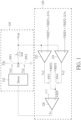
- FIG. 1 is a diagram illustrating a circuitry comprising a regulator 110 and a control circuit 120 according to one embodiment of the present invention.
- the regulator 110 is configured to receive an input signal Vin to generate an output voltage Vout, wherein the input signal Vin has a constant voltage level, and the input signal Vin may be obtained from a battery.
- the regulator 110 comprises a driver 112, a selection circuit comprising two switches SW1 and SW2, and an inductor L, wherein the switch SW1 is coupled between the input signal Vin and a node N1, the switch SW2 is coupled between the node N1 and a ground voltage, and the driver 112 is configured to generate driving signals Vs1 and Vs2 to control the switches SW1 and SW2, respectively.
- a voltage level of the output voltage Vout can be determined. It is noted that the circuit structure of the regulator 110 shown in FIG. 1 is for illustrative, not a limitation of the present invention. In other embodiments, the regulator 110 may have any other suitable design.
- the regulator 110 may be designed in a PMIC of an electronic device such as a mobile phone, and when the electronic device enters a low-power mode or a sleep mode, the regulator 110 is preferred to provide the output voltage Vout with low voltage level, to decrease power loss.
- the control circuit 120 is designed to make the regulator 110 generate an output voltage with a suitable level automatically, to save much more power loss.
- the control circuit 120 comprises two comparators 122 and 124, two switches SW3 and SW4, and an error amplifier 126.
- the comparator 122 is configured to compare the output voltage Vout with a reference voltage VREF3 to generate a control signal Vc1
- the comparator 124 compares the output voltage Vout with a reference voltage VREF to generate a control signal Vc2
- the control signal Vc1 is used to control the switch SW3 to generate a reference voltage VREF2 to serve as an output reference voltage VREF
- the control signal Vc2 is used to control the switch SW4 to generate a reference voltage VREF1 to serve as the output reference voltage VREF.
- the reference voltage VREF1 is greater than the reference voltage VREF2, for example, the reference voltage VREF1 may be 2V, and the reference voltage VREF2 may be 1. 86V; and the reference voltage VREF3 is greater than the reference voltage VREF1, and he reference voltage VREF4 is lower than the reference voltage VREF2, that is VREF3 is equal to "VREF1+ ⁇ Vx", and VREF4 is equal to "VREF2- ⁇ Vy”.
- the control signal Vc1 generated by the comparator 122 when the output voltage Vout is greater than the reference voltage VREF3, the control signal Vc1 generated by the comparator 122 has a high voltage level to enable the switch SW3, so that the reference voltage VREF2 serves as the output reference voltage VREF; and when the output voltage Vout is lower than the reference VREF3, the control signal Vc1 generated by the comparator 122 has a low voltage level to disable the switch SW3.
- the control signal Vc2 generated by the comparator 124 has the high voltage level to enable the switch SW4, so that the reference voltage VREF1 serves as the output reference voltage VREF; and when the output voltage Vout is greater than the reference VREF4, the control signal Vc2 generated by the comparator 124 has the low voltage level to disable the switch SW4.
- the error amplifier 126 compares the output reference voltage VREF with a triangular wave to generate a control signal Vc to control the driver 112.
- the control signal Vc is a square wave, and a duty cycle of the control signal Vc is determined based on the voltage level of the output reference voltage VREF. For example, if the output reference voltage VREF has the low voltage level such as VREF2, the control signal Vc has lower duty cycle, and the driver 112 generates the driving signals Vs1 and Vs2 to decrease an enabling period of the switch SW1 and increase the enabling period of the switch SW2 (the switches SW1 and SW2 are not enabled at the same time), to decrease the voltage level of the output voltage Vout.
- the control signal Vc has greater duty cycle, and the driver 112 generates the driving signals Vs1 and Vs2 to increase an enabling period of the switch SW1 and decrease the enabling period of the switch SW2, to increase the voltage level of the output voltage Vout.
- the reference voltage VREF1 serves as the output reference voltage VREF for the error amplifier 126 to generate the control signal Vc to control the regulator 110 to increase the voltage level of the output voltage Vout.
- the reference voltage VREF2 serves as the output reference voltage VREF for the error amplifier 126 to generate the control signal Vc to control the regulator 110 to decrease the voltage level of the output voltage Vout, to lower the power loss.
- the output voltage Vout is equal to the reference voltage VREF1 when the reference voltage VREF1 serves as the output reference voltage VREF, and output voltage Vout is equal to the reference voltage VREF2 when the reference voltage VREF2 serves as the output reference voltage VREF, but it's not a limitation of the present invention. That is, as long as the voltage level of the output voltage Vout when the error amplifier 126 using the reference voltage VREF1 is higher than when using the reference voltage VREF2, the output voltage Vout does not have to be equal to the reference voltage VREF1/VREF2.
- the control circuit 120 of the present invention can allow the regulator 110 to generate the output voltage Vout with low voltage level most of the time, to effectively decrease the power loss.
- the control circuit 120 can automatically generate the control signal to control the regulator 110 to generate the output voltage with appropriate voltage level, the regulator 410 does not need to receive any indication signal for adjusting the output voltage Vout from the other device when the PMIC operates in the low-power mode, so that the overall design and manufacturing costs of the PMIC can be decreased.
- VREF1, VREF2, ⁇ Vx, ⁇ Vy can be selected from a plurality of voltages.
- a plurality of voltages V1 - Vn are generated by using resistors to divide a voltage V0
- a plurality of voltages ⁇ V1 - ⁇ Vn are generated by using resistors to divide a voltage ⁇ V0.
- the reference voltage VREF1 can be selected from the plurality of voltages V1 - Vn
- the reference voltage VREF2 can be selected from the plurality of voltages V1 - Vn
- each of ⁇ Vx, ⁇ Vy is selected from the plurality of voltages ⁇ V1 - ⁇ Vn.
- FIG. 4 is a diagram illustrating a circuitry comprising a regulator 410 and a control circuit 420 according to one embodiment of the present invention.
- the regulator 410 is configured to receive an input signal Vin to generate an output voltage Vout, wherein the input signal Vin has a constant voltage level, and the input signal Vin may be obtained from a battery.
- the regulator 410 comprises a driver 412, a selection circuit comprising two switches SW1 and SW2, and an inductor L, wherein the switch SW1 is coupled between the input signal Vin and a node N1, the switch SW2 is coupled between the node N1 and a ground voltage, and the driver 412 is configured to generate driving signals Vs1 and Vs2 to control the switches SW1 and SW2, respectively.
- a voltage level of the output voltage Vout can be determined. It is noted that the circuit structure of the regulator 410 shown in FIG. 4 is for illustrative, not a limitation of the present invention. In other embodiments, the regulator 410 may have any other suitable design.
- the regulator 410 may be designed in a PMIC of an electronic device such as a mobile phone, and when the electronic device enters a low-power mode or a sleep mode, the regulator 410 is preferred to provide the output voltage Vout with low voltage level, to decrease power loss.
- the control circuit 420 is designed to make the regulator 410 generate an output voltage with a suitable level automatically, to save much more power loss.
- the control circuit 420 comprises a current sensing circuit 421, two comparators 422 and 424, two switches SW3 and SW4, and an error amplifier 426.
- the current sensing circuit 421 is configured to sense an output current Iout of the regulator 410 to generate a sensed current Iout' , wherein the sensed current Iout' is proportional to the output current Iout.
- the current sensing circuit 421 may use a current mirror to sense a current flowing into the switch SW1, and estimate the sensed current Iout' by using the current flowing into the switch SW1.
- the current sensing circuit 421 may use current mirrors to sense a current flowing into the switch SW1 and a current flowing into the switch SW2, and estimate the sensed current Iout' by using the currents flowing into the switch SW1 and the switch SW2. In yet another embodiment of the present invention, the current sensing circuit 421 may calculate the sensed current Iout' by using a duty cycle of the switch SW1 and the currents flowing into the switch SW1 and the switch SW2.
- the comparator 422 is configured to compare a reference current IREF with the sensed current Iout' to generate a control signal Vc1, and the comparator 424 compares the sensed current Iout' with a reference current IREF to generate a control signal Vc2, wherein the control signal Vc1 is used to control the switch SW3 to generate a reference voltage VREF2 to serve as an output reference voltage VREF, and the control signal Vc2 is used to control the switch SW4 to generate a reference voltage VREF1 to serve as the output reference voltage VREF.
- the reference voltage VREF1 is greater than the reference voltage VREF2, for example, the reference voltage VREF1 may be 2V, and the reference voltage VREF2 may be 1.86V.
- the control signal Vc2 generated by the comparator 424 when the sensed current Iout' is greater than the reference current IREF, the control signal Vc2 generated by the comparator 424 has a high voltage level to enable the switch SW4, so that the reference voltage VREF1 serves as the output reference voltage VREF; and when the sensed current Iout' is lower than the reference current IREF, the control signal Vc1 generated by the comparator 422 has the high voltage level to enable the switch SW3, so that the reference voltage VREF2 serves as the output reference voltage VREF.
- the error amplifier 426 compares the output reference voltage VREF with a triangular wave to generate a control signal Vc to control the driver 412.
- the control signal Vc is a square wave, and a duty cycle of the control signal Vc is determined based on the voltage level of the output reference voltage VREF. For example, if the output reference voltage VREF has the low voltage level such as VREF2, the control signal Vc has lower duty cycle, and the driver 412 generates the driving signals Vs1 and Vs2 to decrease an enabling period of the switch SW1 and increase the enabling period of the switch SW2 (the switches SW1 and SW2 are not enabled at the same time), to decrease the voltage level of the output voltage Vout.
- the control signal Vc has greater duty cycle, and the driver 412 generates the driving signals Vs1 and Vs2 to increase an enabling period of the switch SW1 and decrease the enabling period of the switch SW2, to increase the voltage level of the output voltage Vout.
- the reference voltage VREF1 serves as the output reference voltage VREF for the error amplifier 426 to generate the control signal Vc to control the regulator 410 to increase the voltage level of the output voltage Vout.
- the reference voltage VREF2 serves as the output reference voltage VREF for the error amplifier 426 to generate the control signal Vc to control the regulator 410 to decrease the voltage level of the output voltage Vout, to lower the power loss.
- the output voltage Vout is equal to the reference voltage VREF1 when the reference voltage VREF1 serves as the output reference voltage VREF, and output voltage Vout is equal to the reference voltage VREF2 when the reference voltage VREF2 serves as the output reference voltage VREF, but it's not a limitation of the present invention. That is, as long as the voltage level of the output voltage Vout when the error amplifier 426 using the reference voltage VREF1 is higher than when using the reference voltage VREF2, the output voltage Vout does not have to be equal to the reference voltage VREF1/VREF2.
- the control circuit 420 of the present invention can allow the regulator 410 to generate the output voltage Vout with low voltage level most of the time, to effectively decrease the power loss.
- the control circuit 420 can automatically generate the control signal to control the regulator 410 to generate the output voltage with appropriate voltage level, the regulator 410 does not need to receive any indication signal for adjusting the output voltage Vout from the other device, so that the overall design and manufacturing costs of the PMIC can be decreased.
- the present invention may also be defined by the following numbered clauses.
Landscapes
- Engineering & Computer Science (AREA)
- Physics & Mathematics (AREA)
- General Physics & Mathematics (AREA)
- Theoretical Computer Science (AREA)
- Power Engineering (AREA)
- Electromagnetism (AREA)
- Radar, Positioning & Navigation (AREA)
- Automation & Control Theory (AREA)
- General Engineering & Computer Science (AREA)
- Continuous-Control Power Sources That Use Transistors (AREA)
Abstract
Description
- This application claims the benefit of
U.S. Provisional Application No. 63/313,301, filed on February 24th, 2022 U.S. Provisional Application No. 63/344,078, filed on May 20th, 2022 - When an electronic device enters a low-power mode, most of time a regulator of a power management integrated circuit (PMIC) only needs to provide a very small output current for a back-end circuit to use. In order to avoid the regulator being dropped due to a higher step-up loading, the regulator is designed to always provide a higher output voltage to the back-end circuit. However, the higher step-up loading only occurs for a short period of time, such as one millisecond, so always providing high output voltage will cause high power loss.
- It is therefore an objective of the present invention to provide a regulator, which can automatically generate an output voltage with a suitable level according to a loading of the regulator, to solve the above-mentioned problems.
- According to one embodiment of the present invention, a circuitry comprising a regulator and a control circuit is disclosed. The regulator is configured to receive an input signal to generate an output voltage. The control circuit is configured to select one of a first reference voltage and a second reference voltage to serve as an output reference voltage according to an output signal of the regulator, and generate a control signal according to the output reference voltage to control a voltage level of the output voltage of the regulator.
- According to one embodiment of the present invention, a control method of a regulator disclosed, wherein the regulator is configured to receive an input signal to generate an output voltage. The control method comprises: selecting one of a first reference voltage and a second reference voltage to serve as an output reference voltage according to an output signal of the regulator; and generating a control signal according to the output reference voltage to control a voltage level of the output voltage of the regulator.
- These and other objectives of the present invention will no doubt become obvious to those of ordinary skill in the art after reading the following detailed description of the preferred embodiment that is illustrated in the various figures and drawings.
-
-
FIG. 1 is a diagram illustrating a circuitry comprising a regulator and a control circuit according to one embodiment of the present invention. -
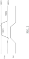
FIG. 2 shows a timing diagram of an output voltage and an output current according to one embodiment of the present invention. -
FIG. 3 shows the generation of VREF1, VREF2, ΔVx and ΔVy according to one embodiment of the present invention. -
FIG. 4 is a diagram illustrating a circuitry comprising a regulator and a control circuit according to another one embodiment of the present invention. -
FIG. 5 shows a timing diagram of an output voltage and an output current according to one embodiment of the present invention. - Certain terms are used throughout the following description and claims to refer to particular system components. As one skilled in the art will appreciate, manufacturers may refer to a component by different names. This document does not intend to distinguish between components that differ in name but not function. In the following discussion and in the claims, the terms "including" and "comprising" are used in an open-ended fashion, and thus should be interpreted to mean "including, but not limited to ...". The terms "couple" and "couples" are intended to mean either an indirect or a direct electrical connection. Thus, if a first device couples to a second device, that connection may be through a direct electrical connection, or through an indirect electrical connection via other devices and connections.
-
FIG. 1 is a diagram illustrating a circuitry comprising aregulator 110 and acontrol circuit 120 according to one embodiment of the present invention. As shown inFIG. 1 , theregulator 110 is configured to receive an input signal Vin to generate an output voltage Vout, wherein the input signal Vin has a constant voltage level, and the input signal Vin may be obtained from a battery. Theregulator 110 comprises adriver 112, a selection circuit comprising two switches SW1 and SW2, and an inductor L, wherein the switch SW1 is coupled between the input signal Vin and a node N1, the switch SW2 is coupled between the node N1 and a ground voltage, and thedriver 112 is configured to generate driving signals Vs1 and Vs2 to control the switches SW1 and SW2, respectively. By using thedriver 112 to control a duty cycle of the switch SW1/SW2, a voltage level of the output voltage Vout can be determined. It is noted that the circuit structure of theregulator 110 shown inFIG. 1 is for illustrative, not a limitation of the present invention. In other embodiments, theregulator 110 may have any other suitable design. - The
regulator 110 may be designed in a PMIC of an electronic device such as a mobile phone, and when the electronic device enters a low-power mode or a sleep mode, theregulator 110 is preferred to provide the output voltage Vout with low voltage level, to decrease power loss. However, because theregulator 110 may suddenly encounter a higher step-up loading, in the conventional art the output voltage Vout should not be designed too low to avoid drop out issue, so that the power loss cannot be effectively decreased. In order to solve this problem, thecontrol circuit 120 is designed to make theregulator 110 generate an output voltage with a suitable level automatically, to save much more power loss. - The
control circuit 120 comprises twocomparators error amplifier 126. In the operation of thecontrol circuit 120, thecomparator 122 is configured to compare the output voltage Vout with a reference voltage VREF3 to generate a control signal Vc1, and thecomparator 124 compares the output voltage Vout with a reference voltage VREF to generate a control signal Vc2, wherein the control signal Vc1 is used to control the switch SW3 to generate a reference voltage VREF2 to serve as an output reference voltage VREF, and the control signal Vc2 is used to control the switch SW4 to generate a reference voltage VREF1 to serve as the output reference voltage VREF. In this embodiment, the reference voltage VREF1 is greater than the reference voltage VREF2, for example, the reference voltage VREF1 may be 2V, and the reference voltage VREF2 may be 1. 86V; and the reference voltage VREF3 is greater than the reference voltage VREF1, and he reference voltage VREF4 is lower than the reference voltage VREF2, that is VREF3 is equal to "VREF1+ΔVx", and VREF4 is equal to "VREF2-ΔVy". In this embodiment, when the output voltage Vout is greater than the reference voltage VREF3, the control signal Vc1 generated by thecomparator 122 has a high voltage level to enable the switch SW3, so that the reference voltage VREF2 serves as the output reference voltage VREF; and when the output voltage Vout is lower than the reference VREF3, the control signal Vc1 generated by thecomparator 122 has a low voltage level to disable the switch SW3. In addition, when the output voltage Vout is lower than the reference voltage VREF4, the control signal Vc2 generated by thecomparator 124 has the high voltage level to enable the switch SW4, so that the reference voltage VREF1 serves as the output reference voltage VREF; and when the output voltage Vout is greater than the reference VREF4, the control signal Vc2 generated by thecomparator 124 has the low voltage level to disable the switch SW4. - Then, the
error amplifier 126 compares the output reference voltage VREF with a triangular wave to generate a control signal Vc to control thedriver 112. Specifically, the control signal Vc is a square wave, and a duty cycle of the control signal Vc is determined based on the voltage level of the output reference voltage VREF. For example, if the output reference voltage VREF has the low voltage level such as VREF2, the control signal Vc has lower duty cycle, and thedriver 112 generates the driving signals Vs1 and Vs2 to decrease an enabling period of the switch SW1 and increase the enabling period of the switch SW2 (the switches SW1 and SW2 are not enabled at the same time), to decrease the voltage level of the output voltage Vout. Similarly, if the output reference voltage VREF has the high voltage level such as VREF1, the control signal Vc has greater duty cycle, and thedriver 112 generates the driving signals Vs1 and Vs2 to increase an enabling period of the switch SW1 and decrease the enabling period of the switch SW2, to increase the voltage level of the output voltage Vout. - Referring to
FIG. 2 , by using the embodiment shown inFIG. 1 , when the loading increases and an output current Iout increases, if the output voltage Vout is lower than the reference voltage VREF4, the reference voltage VREF1 serves as the output reference voltage VREF for theerror amplifier 126 to generate the control signal Vc to control theregulator 110 to increase the voltage level of the output voltage Vout. Then, if the output voltage Vout is greater than the reference voltage VREF3, the reference voltage VREF2 serves as the output reference voltage VREF for theerror amplifier 126 to generate the control signal Vc to control theregulator 110 to decrease the voltage level of the output voltage Vout, to lower the power loss. It is noted that, in the embodiment shown inFIG. 2 , the output voltage Vout is equal to the reference voltage VREF1 when the reference voltage VREF1 serves as the output reference voltage VREF, and output voltage Vout is equal to the reference voltage VREF2 when the reference voltage VREF2 serves as the output reference voltage VREF, but it's not a limitation of the present invention. That is, as long as the voltage level of the output voltage Vout when theerror amplifier 126 using the reference voltage VREF1 is higher than when using the reference voltage VREF2, the output voltage Vout does not have to be equal to the reference voltage VREF1/VREF2. - In the above embodiment, because most of time the
regulator 110 has light load, and the higher step-up loading occurs only a short period such as one or two milliseconds, using thecontrol circuit 120 of the present invention can allow theregulator 110 to generate the output voltage Vout with low voltage level most of the time, to effectively decrease the power loss. In addition, because thecontrol circuit 120 can automatically generate the control signal to control theregulator 110 to generate the output voltage with appropriate voltage level, theregulator 410 does not need to receive any indication signal for adjusting the output voltage Vout from the other device when the PMIC operates in the low-power mode, so that the overall design and manufacturing costs of the PMIC can be decreased. - In one embodiment, VREF1, VREF2, ΔVx, ΔVy can be selected from a plurality of voltages. Taking
FIG. 3 as an example, a plurality of voltages V1 - Vn are generated by using resistors to divide a voltage V0, and a plurality of voltages ΔV1 - ΔVn are generated by using resistors to divide a voltage ΔV0. The reference voltage VREF1 can be selected from the plurality of voltages V1 - Vn, the reference voltage VREF2 can be selected from the plurality of voltages V1 - Vn, and each of ΔVx, ΔVy is selected from the plurality of voltages ΔV1 -ΔVn. -
FIG. 4 is a diagram illustrating a circuitry comprising aregulator 410 and acontrol circuit 420 according to one embodiment of the present invention. As shown inFIG. 4 , theregulator 410 is configured to receive an input signal Vin to generate an output voltage Vout, wherein the input signal Vin has a constant voltage level, and the input signal Vin may be obtained from a battery. Theregulator 410 comprises adriver 412, a selection circuit comprising two switches SW1 and SW2, and an inductor L, wherein the switch SW1 is coupled between the input signal Vin and a node N1, the switch SW2 is coupled between the node N1 and a ground voltage, and thedriver 412 is configured to generate driving signals Vs1 and Vs2 to control the switches SW1 and SW2, respectively. By using thedriver 412 to control a duty cycle of the switch SW1/SW2, a voltage level of the output voltage Vout can be determined. It is noted that the circuit structure of theregulator 410 shown inFIG. 4 is for illustrative, not a limitation of the present invention. In other embodiments, theregulator 410 may have any other suitable design. - The
regulator 410 may be designed in a PMIC of an electronic device such as a mobile phone, and when the electronic device enters a low-power mode or a sleep mode, theregulator 410 is preferred to provide the output voltage Vout with low voltage level, to decrease power loss. However, because theregulator 410 may suddenly encounter a higher step-up loading, in the conventional art the output voltage Vout should not be designed too low to avoid drop out issue, so that the power loss cannot be effectively decreased. In order to solve this problem, thecontrol circuit 420 is designed to make theregulator 410 generate an output voltage with a suitable level automatically, to save much more power loss. - The
control circuit 420 comprises acurrent sensing circuit 421, twocomparators error amplifier 426. In the operation of thecontrol circuit 420, thecurrent sensing circuit 421 is configured to sense an output current Iout of theregulator 410 to generate a sensed current Iout' , wherein the sensed current Iout' is proportional to the output current Iout. In one embodiment, thecurrent sensing circuit 421 may use a current mirror to sense a current flowing into the switch SW1, and estimate the sensed current Iout' by using the current flowing into the switch SW1. In another embodiment, thecurrent sensing circuit 421 may use current mirrors to sense a current flowing into the switch SW1 and a current flowing into the switch SW2, and estimate the sensed current Iout' by using the currents flowing into the switch SW1 and the switch SW2. In yet another embodiment of the present invention, thecurrent sensing circuit 421 may calculate the sensed current Iout' by using a duty cycle of the switch SW1 and the currents flowing into the switch SW1 and the switch SW2. Thecomparator 422 is configured to compare a reference current IREF with the sensed current Iout' to generate a control signal Vc1, and thecomparator 424 compares the sensed current Iout' with a reference current IREF to generate a control signal Vc2, wherein the control signal Vc1 is used to control the switch SW3 to generate a reference voltage VREF2 to serve as an output reference voltage VREF, and the control signal Vc2 is used to control the switch SW4 to generate a reference voltage VREF1 to serve as the output reference voltage VREF. In this embodiment, the reference voltage VREF1 is greater than the reference voltage VREF2, for example, the reference voltage VREF1 may be 2V, and the reference voltage VREF2 may be 1.86V. In this embodiment, when the sensed current Iout' is greater than the reference current IREF, the control signal Vc2 generated by thecomparator 424 has a high voltage level to enable the switch SW4, so that the reference voltage VREF1 serves as the output reference voltage VREF; and when the sensed current Iout' is lower than the reference current IREF, the control signal Vc1 generated by thecomparator 422 has the high voltage level to enable the switch SW3, so that the reference voltage VREF2 serves as the output reference voltage VREF. - Then, the
error amplifier 426 compares the output reference voltage VREF with a triangular wave to generate a control signal Vc to control thedriver 412. Specifically, the control signal Vc is a square wave, and a duty cycle of the control signal Vc is determined based on the voltage level of the output reference voltage VREF. For example, if the output reference voltage VREF has the low voltage level such as VREF2, the control signal Vc has lower duty cycle, and thedriver 412 generates the driving signals Vs1 and Vs2 to decrease an enabling period of the switch SW1 and increase the enabling period of the switch SW2 (the switches SW1 and SW2 are not enabled at the same time), to decrease the voltage level of the output voltage Vout. Similarly, if the output reference voltage VREF has the high voltage level such as VREF1, the control signal Vc has greater duty cycle, and thedriver 412 generates the driving signals Vs1 and Vs2 to increase an enabling period of the switch SW1 and decrease the enabling period of the switch SW2, to increase the voltage level of the output voltage Vout. - Referring to
FIG.5 , by using the embodiment shown inFIG. 4 , when the loading increases and the output current Iout increases, if the sensed current Iout' is greater than the reference current IREF, the reference voltage VREF1 serves as the output reference voltage VREF for theerror amplifier 426 to generate the control signal Vc to control theregulator 410 to increase the voltage level of the output voltage Vout. Then, when the loading decreases and the output current Iout decreases, if the sensed current Iout' is lower than the reference current IREF, the reference voltage VREF2 serves as the output reference voltage VREF for theerror amplifier 426 to generate the control signal Vc to control theregulator 410 to decrease the voltage level of the output voltage Vout, to lower the power loss. It is noted that, in the embodiment shown inFIG. 5 , the output voltage Vout is equal to the reference voltage VREF1 when the reference voltage VREF1 serves as the output reference voltage VREF, and output voltage Vout is equal to the reference voltage VREF2 when the reference voltage VREF2 serves as the output reference voltage VREF, but it's not a limitation of the present invention. That is, as long as the voltage level of the output voltage Vout when theerror amplifier 426 using the reference voltage VREF1 is higher than when using the reference voltage VREF2, the output voltage Vout does not have to be equal to the reference voltage VREF1/VREF2. - In the above embodiment, because most of time the
regulator 410 has light load, and the higher step-up loading occurs only a short period such as one or two milliseconds, using thecontrol circuit 420 of the present invention can allow theregulator 410 to generate the output voltage Vout with low voltage level most of the time, to effectively decrease the power loss. In addition, because thecontrol circuit 420 can automatically generate the control signal to control theregulator 410 to generate the output voltage with appropriate voltage level, theregulator 410 does not need to receive any indication signal for adjusting the output voltage Vout from the other device, so that the overall design and manufacturing costs of the PMIC can be decreased. - Those skilled in the art will readily observe that numerous modifications and alterations of the device and method may be made while retaining the teachings of the invention. Accordingly, the above disclosure should be construed as limited only by the metes and bounds of the appended claims.
- The present invention may also be defined by the following numbered clauses.
- 1. A circuitry, comprising:
- a regulator, configured to receive an input signal to generate an output voltage;
- a control circuit, coupled to the regulator, configured to select one of a first reference voltage and a second reference voltage to serve as an output reference voltage according to an output signal of the regulator, and generate a control signal according to the output reference voltage to control a voltage level of the output voltage of the regulator.
- 2. The circuitry of
clause 1, wherein the output signal is the output voltage, and the control circuit comprises:- a first comparator, configured to compare the output voltage with a third reference voltage to generate a first control signal;
- a second comparator, configured to compare the output voltage with a fourth reference voltage to generate a second control signal;
- a selection circuit, configured to select one of the first reference voltage and the second reference voltage to serve as the output reference voltage according to the first control signal and the second control signal.
- 3. The circuitry of clause 2, wherein the first reference voltage is greater than the second reference voltage, and the third reference voltage is greater than the fourth reference voltage; and when the output voltage is greater than the third reference voltage, the first comparator generates the first control signal to control the selection circuit to select the second reference voltage as the output reference voltage; and when the output voltage is lower than the fourth reference voltage, the second comparator generates the second control signal to control the selection circuit to select the first reference voltage as the output reference voltage.
- 4. The circuitry of clause 3, wherein the third reference voltage is greater than the first reference voltage, and the fourth reference voltage is lower than the second reference voltage.
- 5. The circuitry of clause 3, wherein the selection circuit comprises a first switch and a second switch, the first switch is configured to output the second reference voltage to serve as the output reference voltage, and the second switch is configured to output the first reference voltage to serve as the output reference voltage; and when the when the output voltage is greater than the third reference voltage, the first comparator generates the first control signal to enable the first switch to output the second reference voltage to serve as the output reference voltage, and the second comparator generates the second control signal to disable the second switch; and when the when the output voltage is lower than the fourth reference voltage, the first comparator generates the first control signal to disable the first switch, and the second comparator generates the second control signal to enable the second switch to output the first reference voltage to serve as the output reference voltage.
- 6. The circuitry of clause 3, wherein each of the first reference voltage is selected from a plurality of voltages.
- 7. The circuitry of clause 2, wherein the control circuit further comprises:
an error amplifier, coupled to the selection circuit, configured to compare the output reference voltage with a triangular wave to generate the control signal to control the regulator. - 8. The circuitry of
clause 1, wherein the output signal is an output current of the regulator, and the control circuit comprises:- a first comparator, configured to compare the output current with a reference current to generate a first control signal;
- a second comparator, configured to compare the reference current with the output current to generate a second control signal;
- a selection circuit, configured to select one of the first reference voltage and the second reference voltage to serve as the output reference voltage according to the first control signal and the second control signal.
- 9. The circuitry of clause 8, wherein the first reference voltage is greater than the second reference voltage; and when the output current is greater than the reference current, the second comparator generates the second control signal to control the selection circuit to select the first reference voltage as the output reference voltage; and when the output current is lower than the reference current, the first comparator generates the first control signal to control the selection circuit to select the second reference voltage as the output reference voltage.
- 10. The circuitry of clause 9, wherein the selection circuit comprises a first switch and a second switch, the first switch is configured to output the second reference voltage to serve as the output reference voltage, and the second switch is configured to output the first reference voltage to serve as the output reference voltage; and when the when the output current is greater than the reference current, the first comparator generates the first control signal to disable the first switch, and the second comparator generates the second control signal to enable the second switch to output the first reference voltage to serve as the output reference voltage; and when the output current is lower than the reference current, the first comparator generates the first control signal to enable the first switch to output the second reference voltage to serve as the output reference voltage, and the second comparator generates the second control signal to disable the second switch.
- 11. The circuitry of clause 8, wherein the control circuit further comprises:
an error amplifier, coupled to the selection circuit, configured compare the output reference voltage with a triangular wave to generate the control signal to control the regulator. - 12. A control method of a regulator, wherein the regulator is configured to receive an input signal to generate an output voltage, and the control method comprises:
- selecting one of a first reference voltage and a second reference voltage to serve as an output reference voltage according to an output signal of the regulator; and
- generating a control signal according to the output reference voltage to control a voltage level of the output voltage of the regulator.
- 13. The control method of clause 12, wherein the output signal is the output voltage, and the step of selecting one of the first reference voltage and the second reference voltage to serve as the output reference voltage according to the output signal of the regulator comprises:
- comparing the output voltage with a third reference voltage to generate a first control signal;
- comparing the output voltage with a fourth reference voltage to generate a second control signal;
- selecting one of the first reference voltage and the second reference voltage to serve as the output reference voltage according to the first control signal and the second control signal.
- 14. The control method of clause 13, wherein the first reference voltage is greater than the second reference voltage, and the third reference voltage is greater than the fourth reference voltage; and the step of selecting one of the first reference voltage and the second reference voltage to serve as the output reference voltage according to the first control signal and the second control signal comprises:
- when the output voltage is greater than the third reference voltage, selecting the second reference voltage as the output reference voltage; and
- when the output voltage is lower than the fourth reference voltage, selecting the first reference voltage as the output reference voltage.
- 15. The control method of clause 12, wherein the output signal is an output current of the regulator, and the step of selecting one of the first reference voltage and the second reference voltage to serve as the output reference voltage according to the output signal of the regulator comprises:
- comparing the output current with a reference current to generate a first control signal;
- comparing the reference current with the output current to generate a second control signal;
- selecting one of the first reference voltage and the second reference voltage to serve as the output reference voltage according to the first control signal and the second control signal.
- 16. The control method of clause 15, wherein the first reference voltage is greater than the second reference voltage; and the step of selecting one of the first reference voltage and the second reference voltage to serve as the output reference voltage according to the first control signal and the second control signal comprises:
- when the output current is greater than the reference current, selecting the first reference voltage as the output reference voltage; and
- when the output current is lower than the reference current, selecting the second reference voltage as the output reference voltage.
Claims (15)
- A circuitry, comprising:a regulator (110, 410), configured to receive an input signal to generate an output voltage;a control circuit (120, 420), coupled to the regulator (110, 410), configured to select one of a first reference voltage and a second reference voltage to serve as an output reference voltage according to an output signal of the regulator (110, 410), and generate a control signal according to the output reference voltage to control a voltage level of the output voltage of the regulator (110, 410).
- The circuitry of claim 1, wherein the output signal is the output voltage, and the control circuit (120, 420) comprises:a first comparator (122, 124, 422, 424), configured to compare the output voltage with a third reference voltage to generate a first control signal;a second comparator (122, 124, 422, 424), configured to compare the output voltage with a fourth reference voltage to generate a second control signal;a selection circuit, configured to select one of the first reference voltage and the second reference voltage to serve as the output reference voltage according to the first control signal and the second control signal.
- The circuitry of claim 2, wherein the first reference voltage is greater than the second reference voltage, and the third reference voltage is greater than the fourth reference voltage; and when the output voltage is greater than the third reference voltage, the first comparator (122, 124, 422, 424) generates the first control signal to control the selection circuit to select the second reference voltage as the output reference voltage; and when the output voltage is lower than the fourth reference voltage, the second comparator (122, 124, 422, 424) generates the second control signal to control the selection circuit to select the first reference voltage as the output reference voltage.
- The circuitry of claim 3, wherein the third reference voltage is greater than the first reference voltage, and the fourth reference voltage is lower than the second reference voltage; or
wherein each of the first reference voltage is selected from a plurality of voltages - The circuitry of claim 3, wherein the selection circuit comprises a first switch and a second switch, the first switch is configured to output the second reference voltage to serve as the output reference voltage, and the second switch is configured to output the first reference voltage to serve as the output reference voltage; and when the when the output voltage is greater than the third reference voltage, the first comparator (122, 124, 422, 424) generates the first control signal to enable the first switch to output the second reference voltage to serve as the output reference voltage, and the second comparator (122, 124, 422, 424) generates the second control signal to disable the second switch; and when the when the output voltage is lower than the fourth reference voltage, the first comparator (122, 124, 422, 424) generates the first control signal to disable the first switch, and the second comparator (122, 124, 422, 424) generates the second control signal to enable the second switch to output the first reference voltage to serve as the output reference voltage.
- The circuitry of claim 2, wherein the control circuit (120, 420) further comprises:
an error amplifier (126, 426), coupled to the selection circuit, configured to compare the output reference voltage with a triangular wave to generate the control signal to control the regulator (110, 410). - The circuitry of claim 1, wherein the output signal is an output current of the regulator (110, 410), and the control circuit (120, 420) comprises:a first comparator (122, 124, 422, 424), configured to compare the output current with a reference current to generate a first control signal;a second comparator (122, 124, 422, 424), configured to compare the reference current with the output current to generate a second control signal;a selection circuit, configured to select one of the first reference voltage and the second reference voltage to serve as the output reference voltage according to the first control signal and the second control signal.
- The circuitry of claim 7, wherein the first reference voltage is greater than the second reference voltage; and when the output current is greater than the reference current, the second comparator (122, 124, 422, 424) generates the second control signal to control the selection circuit to select the first reference voltage as the output reference voltage; and when the output current is lower than the reference current, the first comparator (122, 124, 422, 424) generates the first control signal to control the selection circuit to select the second reference voltage as the output reference voltage.
- The circuitry of claim 8, wherein the selection circuit comprises a first switch and a second switch, the first switch is configured to output the second reference voltage to serve as the output reference voltage, and the second switch is configured to output the first reference voltage to serve as the output reference voltage; and when the when the output current is greater than the reference current, the first comparator (122, 124, 422, 424) generates the first control signal to disable the first switch, and the second comparator (122, 124, 422, 424) generates the second control signal to enable the second switch to output the first reference voltage to serve as the output reference voltage; and when the output current is lower than the reference current, the first comparator (122, 124, 422, 424) generates the first control signal to enable the first switch to output the second reference voltage to serve as the output reference voltage, and the second comparator (122, 124, 422, 424) generates the second control signal to disable the second switch.
- The circuitry of claim 7, wherein the control circuit (120, 420) further comprises:
an error amplifier (126, 426), coupled to the selection circuit, configured compare the output reference voltage with a triangular wave to generate the control signal to control the regulator (110, 410). - A control method of a regulator (110, 410), wherein the regulator (110, 410) is configured to receive an input signal to generate an output voltage, and the control method comprises:selecting one of a first reference voltage and a second reference voltage to serve as an output reference voltage according to an output signal of the regulator (110, 410); andgenerating a control signal according to the output reference voltage to control a voltage level of the output voltage of the regulator (110, 410).
- The control method of claim 11, wherein the output signal is the output voltage, and the step of selecting one of the first reference voltage and the second reference voltage to serve as the output reference voltage according to the output signal of the regulator (110, 410) comprises:comparing the output voltage with a third reference voltage to generate a first control signal;comparing the output voltage with a fourth reference voltage to generate a second control signal;selecting one of the first reference voltage and the second reference voltage to serve as the output reference voltage according to the first control signal and the second control signal.
- The control method of claim 12, wherein the first reference voltage is greater than the second reference voltage, and the third reference voltage is greater than the fourth reference voltage; and the step of selecting one of the first reference voltage and the second reference voltage to serve as the output reference voltage according to the first control signal and the second control signal comprises:when the output voltage is greater than the third reference voltage, selecting the second reference voltage as the output reference voltage; andwhen the output voltage is lower than the fourth reference voltage, selecting the first reference voltage as the output reference voltage.
- The control method of claim 11, wherein the output signal is an output current of the regulator (110, 410), and the step of selecting one of the first reference voltage and the second reference voltage to serve as the output reference voltage according to the output signal of the regulator (110, 410) comprises:comparing the output current with a reference current to generate a first control signal;comparing the reference current with the output current to generate a second control signal;selecting one of the first reference voltage and the second reference voltage to serve as the output reference voltage according to the first control signal and the second control signal.
- The control method of claim 14, wherein the first reference voltage is greater than the second reference voltage; and the step of selecting one of the first reference voltage and the second reference voltage to serve as the output reference voltage according to the first control signal and the second control signal comprises:when the output current is greater than the reference current, selecting the first reference voltage as the output reference voltage; andwhen the output current is lower than the reference current, selecting the second reference voltage as the output reference voltage.
Applications Claiming Priority (3)
| Application Number | Priority Date | Filing Date | Title |
|---|---|---|---|
| US202263313301P | 2022-02-24 | 2022-02-24 | |
| US202263344078P | 2022-05-20 | 2022-05-20 | |
| US18/072,724 US12379735B2 (en) | 2022-02-24 | 2022-12-01 | Reference voltage auto-switching mechanism used in regulator for saving more power in low-power mode |
Publications (1)
| Publication Number | Publication Date |
|---|---|
| EP4236046A1 true EP4236046A1 (en) | 2023-08-30 |
Family
ID=84923095
Family Applications (1)
| Application Number | Title | Priority Date | Filing Date |
|---|---|---|---|
| EP23151003.3A Pending EP4236046A1 (en) | 2022-02-24 | 2023-01-10 | Reference voltage auto-switching mechanism used in regulator for saving more power in low-power mode |
Country Status (3)
| Country | Link |
|---|---|
| US (2) | US12379735B2 (en) |
| EP (1) | EP4236046A1 (en) |
| TW (1) | TWI842405B (en) |
Cited By (1)
| Publication number | Priority date | Publication date | Assignee | Title |
|---|---|---|---|---|
| CN117691863A (en) * | 2024-02-01 | 2024-03-12 | 荣耀终端有限公司 | Power management systems and electronic equipment |
Citations (4)
| Publication number | Priority date | Publication date | Assignee | Title |
|---|---|---|---|---|
| US20080284508A1 (en) * | 2007-05-15 | 2008-11-20 | Walker Brett C | Output circuits with class d amplifier |
| US20160267833A1 (en) * | 2015-03-11 | 2016-09-15 | Samsung Display Co., Ltd. | Backlight unit, display apparatus having the same and operating method of backlight unit |
| JP6153732B2 (en) * | 2013-01-21 | 2017-06-28 | リコー電子デバイス株式会社 | Switching regulator |
| CN113014099A (en) * | 2021-04-12 | 2021-06-22 | 成都芯源系统有限公司 | Switching power supply and control circuit and method thereof |
Family Cites Families (5)
| Publication number | Priority date | Publication date | Assignee | Title |
|---|---|---|---|---|
| TWI348262B (en) | 2005-02-10 | 2011-09-01 | Bruno Ferrario | A circuit and method for adaptive frequency compensation for dc-to-dc converter |
| US8493048B2 (en) | 2011-05-23 | 2013-07-23 | Alpha And Omega Semiconductor Incorporated | Constant on-time switching regulator implementing light load control |
| TWI482404B (en) * | 2012-10-05 | 2015-04-21 | Anpec Electronics Corp | Current-limit system and method |
| TWI571029B (en) | 2015-10-28 | 2017-02-11 | 茂達電子股份有限公司 | Compensation circuit and energy storage device using same |
| CN110196611B (en) | 2018-02-27 | 2021-06-29 | 联发科技股份有限公司 | A low dropout voltage regulator and its system |
-
2022
- 2022-12-01 US US18/072,724 patent/US12379735B2/en active Active
-
2023
- 2023-01-10 EP EP23151003.3A patent/EP4236046A1/en active Pending
- 2023-02-21 TW TW112106255A patent/TWI842405B/en active
-
2024
- 2024-12-12 US US18/977,977 patent/US20250110515A1/en active Pending
Patent Citations (5)
| Publication number | Priority date | Publication date | Assignee | Title |
|---|---|---|---|---|
| US20080284508A1 (en) * | 2007-05-15 | 2008-11-20 | Walker Brett C | Output circuits with class d amplifier |
| JP6153732B2 (en) * | 2013-01-21 | 2017-06-28 | リコー電子デバイス株式会社 | Switching regulator |
| US20160267833A1 (en) * | 2015-03-11 | 2016-09-15 | Samsung Display Co., Ltd. | Backlight unit, display apparatus having the same and operating method of backlight unit |
| CN113014099A (en) * | 2021-04-12 | 2021-06-22 | 成都芯源系统有限公司 | Switching power supply and control circuit and method thereof |
| US20220329154A1 (en) * | 2021-04-12 | 2022-10-13 | Chengdu Monolithic Power Systems Co., Ltd. | Switch mode power supply with improved transient performance and control circuit thereof |
Cited By (2)
| Publication number | Priority date | Publication date | Assignee | Title |
|---|---|---|---|---|
| CN117691863A (en) * | 2024-02-01 | 2024-03-12 | 荣耀终端有限公司 | Power management systems and electronic equipment |
| CN117691863B (en) * | 2024-02-01 | 2024-05-24 | 荣耀终端有限公司 | Power management system and electronic equipment |
Also Published As
| Publication number | Publication date |
|---|---|
| US20250110515A1 (en) | 2025-04-03 |
| US20230266781A1 (en) | 2023-08-24 |
| US12379735B2 (en) | 2025-08-05 |
| TW202335410A (en) | 2023-09-01 |
| TWI842405B (en) | 2024-05-11 |
Similar Documents
| Publication | Publication Date | Title |
|---|---|---|
| US8085011B1 (en) | Boost regulator using synthetic ripple regulation | |
| US8013587B2 (en) | DC/DC power supply circuit with a bypass circuit | |
| US8362748B2 (en) | Voltage comparison circuit | |
| US7078882B2 (en) | Active clamping circuit and power supply system using the same | |
| US6979985B2 (en) | Switching power supply device and switching power supply system | |
| US8040121B2 (en) | Switching regulator | |
| KR101497918B1 (en) | Bidirectional power converter | |
| US8018210B2 (en) | Voltage converting circuit and method thereof | |
| JP5287191B2 (en) | Hysteresis switching regulator and operation control method thereof | |
| US7960946B2 (en) | Power supply circuit, power supply control circuit, and power supply control method | |
| CN101218735A (en) | Step-down switching regulator and its control circuit, electronic equipment using it | |
| JP2005086931A (en) | Switching power supply and semiconductor integrated circuit used for it | |
| US20170126045A1 (en) | Compensation circuit and energy storage device thereof | |
| CN111682763A (en) | Voltage converter, controller and control method thereof | |
| CN101981525A (en) | Power source device and output voltage changing method of the power source device | |
| US7279869B2 (en) | PFM control circuit for DC regulator | |
| US6969981B1 (en) | Voltage regulator power management apparatus | |
| CN111596715A (en) | Voltage adjusting device, chip, power supply and electronic equipment | |
| US20250110515A1 (en) | Reference voltage auto-switching mechanism used in regulator for saving more power in low-power mode | |
| KR102856358B1 (en) | A DC to DC converter and a integrated circuit including the same | |
| US12218573B2 (en) | Control circuit for DC-DC converters with nonlinear adaptive voltage position and control method thereof | |
| CN112290646A (en) | Lithium battery charging method and device | |
| CN113906661B (en) | Technology for controlling single-inductor multi-output (SIMO) switch-mode power supplies (SMPS) | |
| KR20230110093A (en) | Charge integrated circuit including bidirectional switching converter, and electronic device including same | |
| CN211857324U (en) | Voltage adjusting device, chip, power supply and electronic equipment |
Legal Events
| Date | Code | Title | Description |
|---|---|---|---|
| PUAI | Public reference made under article 153(3) epc to a published international application that has entered the european phase |
Free format text: ORIGINAL CODE: 0009012 |
|
| STAA | Information on the status of an ep patent application or granted ep patent |
Free format text: STATUS: THE APPLICATION HAS BEEN PUBLISHED |
|
| AK | Designated contracting states |
Kind code of ref document: A1 Designated state(s): AL AT BE BG CH CY CZ DE DK EE ES FI FR GB GR HR HU IE IS IT LI LT LU LV MC ME MK MT NL NO PL PT RO RS SE SI SK SM TR |
|
| STAA | Information on the status of an ep patent application or granted ep patent |
Free format text: STATUS: REQUEST FOR EXAMINATION WAS MADE |
|
| 17P | Request for examination filed |
Effective date: 20240221 |
|
| RBV | Designated contracting states (corrected) |
Designated state(s): AL AT BE BG CH CY CZ DE DK EE ES FI FR GB GR HR HU IE IS IT LI LT LU LV MC ME MK MT NL NO PL PT RO RS SE SI SK SM TR |
|
| STAA | Information on the status of an ep patent application or granted ep patent |
Free format text: STATUS: EXAMINATION IS IN PROGRESS |
|
| 17Q | First examination report despatched |
Effective date: 20250422 |