EP4235954A1 - Isolation method for radio frequency power amplifier transmission line, and transmission structure - Google Patents
Isolation method for radio frequency power amplifier transmission line, and transmission structure Download PDFInfo
- Publication number
- EP4235954A1 EP4235954A1 EP22879607.4A EP22879607A EP4235954A1 EP 4235954 A1 EP4235954 A1 EP 4235954A1 EP 22879607 A EP22879607 A EP 22879607A EP 4235954 A1 EP4235954 A1 EP 4235954A1
- Authority
- EP
- European Patent Office
- Prior art keywords
- transmission lines
- layer
- permalloy
- wall
- radio frequency
- Prior art date
- Legal status (The legal status is an assumption and is not a legal conclusion. Google has not performed a legal analysis and makes no representation as to the accuracy of the status listed.)
- Granted
Links
Images


Classifications
-
- H—ELECTRICITY
- H01—ELECTRIC ELEMENTS
- H01P—WAVEGUIDES; RESONATORS, LINES, OR OTHER DEVICES OF THE WAVEGUIDE TYPE
- H01P3/00—Waveguides; Transmission lines of the waveguide type
- H01P3/02—Waveguides; Transmission lines of the waveguide type with two longitudinal conductors
- H01P3/08—Microstrips; Strip lines
-
- H—ELECTRICITY
- H03—ELECTRONIC CIRCUITRY
- H03F—AMPLIFIERS
- H03F3/00—Amplifiers with only discharge tubes or only semiconductor devices as amplifying elements
- H03F3/20—Power amplifiers, e.g. Class B amplifiers, Class C amplifiers
- H03F3/24—Power amplifiers, e.g. Class B amplifiers, Class C amplifiers of transmitter output stages
-
- H—ELECTRICITY
- H01—ELECTRIC ELEMENTS
- H01P—WAVEGUIDES; RESONATORS, LINES, OR OTHER DEVICES OF THE WAVEGUIDE TYPE
- H01P11/00—Apparatus or processes specially adapted for manufacturing waveguides or resonators, lines, or other devices of the waveguide type
- H01P11/001—Manufacturing waveguides or transmission lines of the waveguide type
- H01P11/003—Manufacturing lines with conductors on a substrate, e.g. strip lines, slot lines
-
- H—ELECTRICITY
- H03—ELECTRONIC CIRCUITRY
- H03F—AMPLIFIERS
- H03F3/00—Amplifiers with only discharge tubes or only semiconductor devices as amplifying elements
- H03F3/60—Amplifiers in which coupling networks have distributed constants, e.g. with waveguide resonators
-
- H—ELECTRICITY
- H04—ELECTRIC COMMUNICATION TECHNIQUE
- H04B—TRANSMISSION
- H04B3/00—Line transmission systems
- H04B3/02—Details
- H04B3/32—Reducing cross-talk, e.g. by compensating
-
- H—ELECTRICITY
- H05—ELECTRIC TECHNIQUES NOT OTHERWISE PROVIDED FOR
- H05K—PRINTED CIRCUITS; CASINGS OR CONSTRUCTIONAL DETAILS OF ELECTRIC APPARATUS; MANUFACTURE OF ASSEMBLAGES OF ELECTRICAL COMPONENTS
- H05K9/00—Screening of apparatus or components against electric or magnetic fields
- H05K9/0073—Shielding materials
- H05K9/0081—Electromagnetic shielding materials, e.g. EMI, RFI shielding
-
- H—ELECTRICITY
- H03—ELECTRONIC CIRCUITRY
- H03F—AMPLIFIERS
- H03F2200/00—Indexing scheme relating to amplifiers
- H03F2200/451—Indexing scheme relating to amplifiers the amplifier being a radio frequency amplifier
-
- Y—GENERAL TAGGING OF NEW TECHNOLOGICAL DEVELOPMENTS; GENERAL TAGGING OF CROSS-SECTIONAL TECHNOLOGIES SPANNING OVER SEVERAL SECTIONS OF THE IPC; TECHNICAL SUBJECTS COVERED BY FORMER USPC CROSS-REFERENCE ART COLLECTIONS [XRACs] AND DIGESTS
- Y02—TECHNOLOGIES OR APPLICATIONS FOR MITIGATION OR ADAPTATION AGAINST CLIMATE CHANGE
- Y02D—CLIMATE CHANGE MITIGATION TECHNOLOGIES IN INFORMATION AND COMMUNICATION TECHNOLOGIES [ICT], I.E. INFORMATION AND COMMUNICATION TECHNOLOGIES AIMING AT THE REDUCTION OF THEIR OWN ENERGY USE
- Y02D30/00—Reducing energy consumption in communication networks
- Y02D30/70—Reducing energy consumption in communication networks in wireless communication networks
Definitions
- the present disclosure relates to a technical field of wireless communications, and in particular to a method for isolating transmission lines of a radio frequency power amplifier and a transmission structure for the radio frequency power amplifier.
- Wireless communications refer to long-distance communications which are performed without conductors or cables for transmitting among a plurality of nodes, and the wireless communications may be performed through radio, wireless, etc.
- radio frequency power amplifiers serving as one important device for communication, mainly play a role in amplifying radio frequency signals, thereby improving communication quality.
- the present disclosure aims to provide a method for isolating transmission lines of a radio frequency power amplifier and a transmission structure for the radio frequency power amplifier to solve a problem that isolation between transmission lines on a chip substrate of current radio frequency power amplifiers is relatively poor, thereby affecting communication quality.
- the present disclosure provides a method for isolating transmission lines of a radio frequency power amplifier, including:
- depths of the plurality of the grooves are equal and are smaller than thickness of the aluminum layer, and the plurality of the grooves are disposed on the outer wall of the aluminum layer at equal intervals.
- wrapping the permalloy layer on the outer wall of each of the transmission lines includes following steps:
- a material of the insulation paste is 2025DSI, and a thickness of the permalloy layer is 40 ⁇ m - 50 ⁇ m.
- the wrapping the permalloy layer on the outer wall of each of the transmission lines further includes a following step: placing the transmission lines each wrapped and fixed with the permalloy layer in a high-temperature oven to be heated to 150°C and then taking out the transmission lines each wrapped and fixed with the permalloy layer in the high-temperature oven.
- wrapping the aluminum layer on the outer wall of the permalloy layer includes following steps:
- a material of the insulation paste is 2025DSI, and a thickness of the aluminum layer is 35 ⁇ m-45 ⁇ m.
- the wrapping the aluminum layer on the outer wall of the permalloy layer further includes a following step: placing the transmission lines each wrapped and fixed with the aluminum layer in a high-temperature oven to be heated to 150°C and then taking out the transmission lines each wrapped and fixed with the aluminum layer in the high-temperature oven.
- a depth of each of the plurality of the grooves is 20 ⁇ m-25 ⁇ m, and a distance between adjacent two of the plurality of the grooves is 0.5 mm-0.8 mm.
- the shielding lines are made of an insulation material, a width of each of the shielding lines is 50 ⁇ m-65 ⁇ m, and a length of each of the shielding lines is greater than or equal to a length of each of the transmission lines.
- the present disclosure further provides a transmission structure for a radio frequency power amplifier, including a chip substrate and at least two transmission lines.
- the at least two transmission lines are disposed on the chip substrate.
- a distance between adjacent two of the at least two transmission lines is greater than 2.5 times a width of each of the at least two transmission lines.
- Shielding lines are disposed at an inner side of each of the at least two transmission lines and an outer side of each of the at least two transmission lines opposite to the inner side.
- a permalloy layer is wrapped on an outer wall of each of the at least two transmission lines, an aluminum layer is wrapped on an outer wall of the permalloy layer, and a plurality of grooves are defined on an outer wall of the aluminum layer at intervals, where the plurality of the grooves are recessed inward and in an inverted triangular structure.
- the method for isolating the transmission lines of the radio frequency power amplifier sets the distance between adjacent two of the transmission lines on the chip substrate to be greater than 2.5 times the width of each of the transmission lines, disposes the shielding lines at the inner side of each of the transmission lines and the outer side of each of the transmission lines opposite to the inner side, wraps the permalloy layer on the outer wall of each of the transmission lines, wraps the aluminum layer on the outer wall of the permalloy layer, and defines the plurality of the grooves on the outer wall of the aluminum layer at intervals, where the plurality of the grooves are recessed inward and in the inverted triangular structure.
- the isolation between the adjacent two of the transmission lines is enhanced and influence on radio frequency signals, transmitted by the transmission lines, by parasitic capacitance between the transmission lines, is reduced, through setting the distance between adjacent two of the transmission lines on the chip substrate and disposing the shielding lines.
- interference to radio frequency signals, transmitted in the transmission lines, by an induced magnetic field existing between the adjacent two of the transmission lines is avoided through the wrapping of the permalloy layer, which further enhances the isolation between the adjacent two of the transmission lines; and interference to the radio frequency, transmitted in the transmission lines, by external electromagnetic waves, is avoided through the wrapping of the aluminum layer and the disposing of the plurality of the grooves, so as to enhance isolation between the transmission lines and the outside.
- One embodiment of the present disclosure provides a method for isolating transmission lines 2 of a radio frequency power amplifier, as shown in FIGS. 1 and 4 , including following steps.
- Step S100 setting a distance between adjacent two of transmission lines 2 on a chip substrate 1 to be greater than 2.5 times a width of each of the transmission lines 2, and disposing shielding lines 3 at an inner side of each of the transmission lines 2 and an outer side of each of the transmission lines 2 opposite to the inner side.
- a width of each of the transmission lines 2 is a long edge distance of the rectangle; if the cross section of each of the transmission lines 2 is a circle, the width of each of the transmission lines is a diameter of the circle; and if the cross section of each of the transmission lines 2 is in another shape, the width of each of the transmission lines 2 is an average between a distance between two nearest points and a distance between two farthest points of the corresponding shape.
- the distance between the adjacent two of the transmission lines 2 is preset on the chip substrate 1, and when assembling, the transmission lines 2 are disposed according to the distance preset on the chip substrate 1.
- an increased distance between the adjacent two of the transmission lines 2 is set according to rules of plate-making technology of the chip substrate 1. Furthermore, the distance between the adjacent two of the transmission lines 2 on the chip substrate 1 is equal to 3 times the width (line width) of each of the transmission lines 2.
- the inner side and the outer side opposite to the inner side of the each of the transmission lines are based on the chip substrate 1.
- the shielding lines 3 are disposed at the inner side of each of the transmission lines 2 and the outer side of each of the transmission lines 2 opposite to the inner side of the radio frequency power amplifier on the chip substrate 1.
- the shielding lines may be disposed on an outer wall of each of the transmission lines, or may be disposed at a position, with respect to the inner side and the outer side of each of the transmission lines, of the chip substrate 1.
- the shielding lines 3 are made of an insulation material, and a length of each of the shielding lines is greater than or equal to a length of each of the transmission lines.
- a width of each of the shielding lines 3 is 50 ⁇ m-65 ⁇ m. Certainly, the width of each of the shielding lines 3 may also be adaptively adjusted according to actual requirements.
- a width of each of the shielding lines 3 is a long edge distance of the rectangle; if the cross section of each of the shielding lines 3 is a circle, the width of each of the transmission lines is a diameter of the circle; and if the cross section of each of the shielding lines 3 is in another shape, the width of each of the shielding lines 3 is an average between a distance between two nearest points and a distance between two farthest points of the corresponding shape.
- the adjacent two of the transmission lines 2 on the chip substrate 1 is set to be greater than 2.5 times the width of each of the transmission lines 2, and the shielding lines 3 are disposed at the inner side of each of the transmission lines 2 and the outer side of each of the transmission lines 2 opposite to the inner side, the adjacent two of the transmission lines may be separated from each other to enhance isolation between the adjacent two of the transmission lines and further reduce influence on radio frequency signals, transmitted by the transmission lines 2, by parasitic capacitance between the transmission lines 2.
- Step S200 wrapping a permalloy layer 4 on an outer wall of each of the transmission lines 2.
- the step S200 wraps the permalloy layer 4 on the outer wall of each of the transmission lines 2, so that outer walls of all of the transmission lines 2 each is wrapped with the permalloy layer 4.
- the step S200 includes following sub-steps.
- Step S201 measuring a length of each of the transmission lines 2, and serving the length of each of the transmission lines 2 as a length of the permalloy layer 4.
- Step S202 measuring a perimeter of each of the transmission lines 2, and serving the perimeter of each of the transmission lines 2 as a width of the permalloy layer 4.
- Step S203 cutting out the permalloy layer 4 corresponding to each of the transmission lines 2 from a permalloy material according to the length of the permalloy layer 4 and the width of the permalloy layer 4.
- Step S204 uniformly coating one side of the permalloy layer 4 with an insulation paste, and wrapping and fixing the one side coated with the insulation paste of the permalloy layer 4 on the outer wall of each of the transmission lines 2.
- the steps S201-S204 are steps of wrapping the permalloy layer 4 on an outer wall of a single one of the transmission lines 2.
- the length and the perimeter of each of the transmission lines 2 may be obtained through measurement tools, or may be directly obtained according to parameters for manufacturing the chip substrate 1; and when cutting out, a corresponding cutting tool may be used for cutting out.
- a material of the insulation paste is 2025DSI, and a thickness of the permalloy layer 4 is 40 ⁇ m - 50 ⁇ m.
- insulation paste of other materials may also be selected and a thickness of the insulation paste may further be adaptively adjusted.
- the step S200 further includes a step of placing the transmission lines 2 each wrapped and fixed with the permalloy layer 4 in a high-temperature oven to be heated to 150°C and then taking out the transmission lines 2 each wrapped and fixed with the permalloy layer 4 in the high-temperature oven.
- the insulation paste is waited to completely melt, so that the insulation paste may be fully fused with the permalloy layer 4 and each of the transmission lines 2 for being taken out. In this way, stability and firmness of connection between the permalloy layer 4 and each of the transmission lines 2 may be improved.
- the step of placing the chip substrate 1 in the high-temperature oven to be heated is performed after the step of wrapping the permalloy layer 4 on the outer wall of each of the transmission lines 2.
- the permalloy layer 4 is made of a high magnetic permeability material, through wrapping the permalloy layer 4 on the outer wall of each of the transmission lines 2, when radio frequency signals pass in the transmission lines to generate an induced magnetic field, so that magnetic induction lines emitted by the induced magnetic field are enabled to move along an outer surface layer of the permalloy layer 4, no induction current is formed in the transmission lines 2, and therefore the radio frequency signals transmitted in the transmission lines 2 may not be interfered, so as to enhance the isolation between the adjacent two of the transmission lines 2.
- Step S300 wrapping an aluminum layer 5 on an outer wall of the permalloy layer 4, defining a plurality of grooves 51 on an outer wall of the aluminum layer 5 at intervals, where the plurality of the grooves 51 are recessed inward and in an inverted triangular structure.
- the permalloy layer 4 is wrapped on the outer wall of each of the transmission lines 2, and is performed until the isolating paste in the step S200 is cooled and solidified.
- the aluminum layer 5 is wrapped on the outer wall of the permalloy layer 4, so that each of the transmission lines 2 is wrapped with the aluminum layer 5.
- the step 300 includes following sub-steps.
- the steps S301-S304 are steps of wrapping the aluminum layer 5 on an outer wall of a single one of the permalloy layer 4.
- the length of each of the transmission lines 2 is measured in the step S201, so that the length of each of the transmission lines 2 may be obtained without measurement, and a perimeter of the permalloy layer 4 is the width of the permalloy layer 4, which is measured in the step S202, and the perimeter of the permalloy layer 4 may be obtained without measurement.
- a material of the insulation paste is 2025DSI, and a thickness of the permalloy layer 4 is 35 ⁇ m - 45 ⁇ m.
- insulation paste of other materials may also be selected and a thickness of the insulation paste may further be adaptively adjusted.
- the step S304 further includes a step of placing the transmission lines 2 each wrapped and fixed with the aluminum layer 5 in a high-temperature oven to be heated to 150°C and then taking out the transmission lines 2 each wrapped and fixed with the aluminum layer 5 in the high-temperature oven. After the transmission lines 2 are heated to 150°C and wait for completely melting the insulation paste, so that the insulation paste is fully fused with the permalloy layer 4 and the aluminum layer 5 and then taken out. In this way, stability and firmness of connection between the permalloy layer 4 and the aluminum layer 5 are improved.
- the step of placing the chip substrate 1 in the high-temperature oven to be heated is performed after the step of wrapping the aluminum layer 5 on the outer wall of each of the permalloy layer 4.
- the plurality of the grooves 51 is performed after cutting out the aluminum layer 5 in the step S303, and the step S304 is performed after forming the plurality of the grooves 51.
- depths of the plurality of the grooves 51 are equal and are smaller than thickness of the aluminum layer 5, and the plurality of the grooves 51 are disposed on the outer wall of the aluminum layer 5 at equal intervals.
- a depth of each of the plurality of the grooves 51 is 20 ⁇ m-25 ⁇ m, and a distance between adjacent two of the plurality of the grooves 51 is 0.5 mm-0.8 mm.
- the aluminum layer 5 is wrapped on the outer wall of the permalloy layer 4, the plurality of the grooves 51 which are recessed inward and in the inverted triangular structure are defined on the outer wall of the aluminum layer 5 at intervals, thereby isolating the external electromagnetic waves through the aluminum layer 5.
- two inclined surfaces in each of the plurality of the grooves 51 in the inverted triangular structure may reflect electromagnetic waves, so that the electromagnetic waves of the two inclined surfaces cancel each other, and interference on radio frequency signals in the transmission lines 2 by the external electromagnetic waves is avoided, thereby enhancing the isolation between the transmission lines 2 and the outside.
- the transmission lines 2 in the embodiment are assembled on the chip substrate 1 after completing steps S100-S300. At this time, the aluminum layer 5 at the outermost layer of the transmission lines is assembled on the chip substrate 1 through bonding, welding, etc.
- the step S100 may be performed after completing the step S200 and the step S300.
- the permalloy layer 4 is wrapped on each of the transmission lines 2.
- the transmission lines 2 and the shielding lines 3 are assembled on chip substrate 1, the length of each of the transmission lines is measured to be the length of the permalloy layer 4 and the aluminum layer 5, and the perimeter of a portion of each of the transmission lines 2 that is not in contact with the chip substrate 1 is measured to be the width of the permalloy layer4, and the permalloy layer 4 is cut out for wrapping.
- a perimeter of a portion of the permalloy layer 4 that is not in contact with the chip substrate 1 is measured to be the width of the aluminum layer 5, and the aluminum layer 5 is cut out for wrapping, thereby the method for isolating the transmission lines of the radio frequency power amplifier is completed.
- the transmission lines 2 are assembled on the chip substrate 1 through bonding, welding, etc.
- the method for isolating the transmission lines of the radio frequency power amplifier of the present disclosure increases the distance between the adjacent two of the transmission lines 2, provides the shielding lines 3 on two opposite sides of each of the transmission lines 2, wraps the permalloy layer 4 on the outer wall of each of the transmission lines 2, then wraps the aluminum layer 5 on the outer wall of the permalloy layer 4, and provides the plurality of the grooves 51 of the inverted triangular structure on the outer wall of the aluminum layer 5. Therefore, the isolation between the adjacent two of the transmission lines 2 is enhanced through increasing the distance between the adjacent two of the transmission lines 2 and disposing the shielding lines 3, moreover, the influence on the radio frequency signals, transmitted by the transmission lines 2, by the parasitic capacitance between the transmission lines 2 is reduced.
- interference to the radio frequency signals, transmitted in the transmission lines 2, by an induced magnetic field existing between the adjacent two of the transmission lines 2, is avoided through the wrapping of the permalloy layer 4, which further enhances the isolation between the adjacent two of the transmission lines 2; and interference to the radio frequency, transmitted in the transmission lines 2, by external electromagnetic waves, is avoided through the wrapping of the aluminum layer 4 and the disposing of the plurality of the grooves 5, so as to enhance the isolation between the transmission lines 2 and the outside.
- the present disclosure further provides another embodiment, the embodiment provides a transmission structure for the radio frequency power amplifier.
- a transmission structure for the radio frequency power amplifier As shown in FIGS. 4 or 5 , including a chip substrate 1 and at least two transmission lines 2.
- the at least two transmission lines 2 are disposed on the chip substrate 1.
- a distance between adjacent two of the at least two transmission lines 2 is greater than 2.5 times a width of each of the at least two transmission lines 2.
- Shielding lines 3 are disposed at an inner side of each of the at least two transmission lines 2 and an outer side of each of the at least two transmission lines 2 opposite to the inner side.
- a permalloy layer 4 is wrapped on an outer wall of each of the at least two transmission lines 2, an aluminum layer 5 is wrapped on an outer wall of the permalloy layer 4, and a plurality of grooves 51 are defined on an outer wall of the aluminum layer 5 at intervals, where the plurality of the grooves 51 are recessed inward and in an inverted triangular structure.
- the distance between the adjacent two of the at least two transmission lines 2 is greater than 3 times the width of each of the at least two transmission lines 2.
- the shielding lines 3, the permalloy layer 4, the aluminum layer 5, and the plurality of the grooves 51 on the aluminum layer 5 are all set according to the method for isolating the transmission lines 2 of the radio frequency power amplifier. Therefore, the transmission structure of the radio frequency power amplifier in the embodiment may also achieve the technical effect achieved by the method for isolating the transmission lines 2 of the radio frequency power amplifier in foregoing embodiments.
Landscapes
- Engineering & Computer Science (AREA)
- Power Engineering (AREA)
- Physics & Mathematics (AREA)
- Microelectronics & Electronic Packaging (AREA)
- Electromagnetism (AREA)
- Signal Processing (AREA)
- Computer Networks & Wireless Communication (AREA)
- Manufacturing & Machinery (AREA)
- Shielding Devices Or Components To Electric Or Magnetic Fields (AREA)
- Semiconductor Integrated Circuits (AREA)
- Structure Of Printed Boards (AREA)
- Amplifiers (AREA)
- Microwave Amplifiers (AREA)
Abstract
Description
- The present disclosure relates to a technical field of wireless communications, and in particular to a method for isolating transmission lines of a radio frequency power amplifier and a transmission structure for the radio frequency power amplifier.
- Wireless communications refer to long-distance communications which are performed without conductors or cables for transmitting among a plurality of nodes, and the wireless communications may be performed through radio, wireless, etc. In a process of performing the wireless communications, radio frequency power amplifiers, serving as one important device for communication, mainly play a role in amplifying radio frequency signals, thereby improving communication quality.
- However, isolation between transmission lines on a chip substrate of current radio frequency power amplifiers is poor when the radio frequency power amplifiers work in practice, therefore easily causing interference between the transmission lines. Moreover, external electromagnetic waves may also interfere with the transmission lines, thereby causing interference to radio frequency signals transmitted in the transmission lines, and further affecting the communication quality.
- The present disclosure aims to provide a method for isolating transmission lines of a radio frequency power amplifier and a transmission structure for the radio frequency power amplifier to solve a problem that isolation between transmission lines on a chip substrate of current radio frequency power amplifiers is relatively poor, thereby affecting communication quality.
- According to a first aspect, the present disclosure provides a method for isolating transmission lines of a radio frequency power amplifier, including:
- setting a distance between adjacent two of transmission lines on a chip substrate to be greater than 2.5 times a width of each of the transmission lines, and disposing shielding lines at an inner side of each of the transmission lines and an outer side of each of the transmission lines opposite to the inner side;
- wrapping a permalloy layer on an outer wall of each of the transmission lines; and
- wrapping an aluminum layer on an outer wall of the permalloy layer, defining a plurality of grooves on an outer wall of the aluminum layer at intervals, where the plurality of the grooves are recessed inward and in an inverted triangular structure.
- Furthermore, depths of the plurality of the grooves are equal and are smaller than thickness of the aluminum layer, and the plurality of the grooves are disposed on the outer wall of the aluminum layer at equal intervals.
- Furthermore, the wrapping the permalloy layer on the outer wall of each of the transmission lines includes following steps:
- measuring a length of each of the transmission lines, and serving the length of each of the transmission lines as a length of the permalloy layer;
- measuring a perimeter of each of the transmission lines, and serving the perimeter of each of the transmission lines as a width of the permalloy layer;
- cutting out the permalloy layer corresponding to each of the transmission lines from a permalloy material according to the length of the permalloy layer and the width of the permalloy layer; and
- uniformly coating one side of the permalloy layer with an insulation paste, and wrapping and fixing the one side coated with the insulation paste of the permalloy layer on the outer wall of each of the transmission lines.
- Furthermore, a material of the insulation paste is 2025DSI, and a thickness of the permalloy layer is 40 µm - 50 µm.
- Furthermore, the wrapping the permalloy layer on the outer wall of each of the transmission lines further includes a following step:
placing the transmission lines each wrapped and fixed with the permalloy layer in a high-temperature oven to be heated to 150°C and then taking out the transmission lines each wrapped and fixed with the permalloy layer in the high-temperature oven. - Furthermore, the wrapping the aluminum layer on the outer wall of the permalloy layer includes following steps:
- measuring a length of each of the transmission lines, and serving the length of each of the transmission lines as a length of the aluminum layer;
- measuring a perimeter of each of the transmission lines, and serving the perimeter of each of the transmission lines as a width of the aluminum layer;
- cutting out the aluminum layer corresponding to the permalloy layer from an aluminum material according to the length of the aluminum layer and the width of the aluminum layer; and
- uniformly coating one side of the aluminum layer with an insulation paste, and wrapping and fixing the one side coated with the insulation paste of the aluminum layer on the outer wall of the permalloy layer.
- Furthermore, a material of the insulation paste is 2025DSI, and a thickness of the aluminum layer is 35 µm-45 µm.
- Furthermore, the wrapping the aluminum layer on the outer wall of the permalloy layer further includes a following step:
placing the transmission lines each wrapped and fixed with the aluminum layer in a high-temperature oven to be heated to 150°C and then taking out the transmission lines each wrapped and fixed with the aluminum layer in the high-temperature oven. - Furthermore, a depth of each of the plurality of the grooves is 20 µm-25 µm, and a distance between adjacent two of the plurality of the grooves is 0.5 mm-0.8 mm.
- Furthermore, the shielding lines are made of an insulation material, a width of each of the shielding lines is 50 µm-65 µm, and a length of each of the shielding lines is greater than or equal to a length of each of the transmission lines.
- According to a second aspect, the present disclosure further provides a transmission structure for a radio frequency power amplifier, including a chip substrate and at least two transmission lines. The at least two transmission lines are disposed on the chip substrate. A distance between adjacent two of the at least two transmission lines is greater than 2.5 times a width of each of the at least two transmission lines. Shielding lines are disposed at an inner side of each of the at least two transmission lines and an outer side of each of the at least two transmission lines opposite to the inner side. A permalloy layer is wrapped on an outer wall of each of the at least two transmission lines, an aluminum layer is wrapped on an outer wall of the permalloy layer, and a plurality of grooves are defined on an outer wall of the aluminum layer at intervals, where the plurality of the grooves are recessed inward and in an inverted triangular structure.
- Compared with the prior art, the method for isolating the transmission lines of the radio frequency power amplifier sets the distance between adjacent two of the transmission lines on the chip substrate to be greater than 2.5 times the width of each of the transmission lines, disposes the shielding lines at the inner side of each of the transmission lines and the outer side of each of the transmission lines opposite to the inner side, wraps the permalloy layer on the outer wall of each of the transmission lines, wraps the aluminum layer on the outer wall of the permalloy layer, and defines the plurality of the grooves on the outer wall of the aluminum layer at intervals, where the plurality of the grooves are recessed inward and in the inverted triangular structure. Therefore, the isolation between the adjacent two of the transmission lines is enhanced and influence on radio frequency signals, transmitted by the transmission lines, by parasitic capacitance between the transmission lines, is reduced, through setting the distance between adjacent two of the transmission lines on the chip substrate and disposing the shielding lines. Moreover, interference to radio frequency signals, transmitted in the transmission lines, by an induced magnetic field existing between the adjacent two of the transmission lines, is avoided through the wrapping of the permalloy layer, which further enhances the isolation between the adjacent two of the transmission lines; and interference to the radio frequency, transmitted in the transmission lines, by external electromagnetic waves, is avoided through the wrapping of the aluminum layer and the disposing of the plurality of the grooves, so as to enhance isolation between the transmission lines and the outside.
- In order to more clearly illustrate technical solutions in embodiments of the present disclosure, drawings that need to be used in description of the embodiments are briefly described below, and it is obvious that the drawings in the following description are merely some embodiments of the present disclosure, and those skilled in the art may obtain other drawings according to these drawings without involving any inventive effort.
-
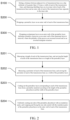
FIG. 1 is a flow diagram of a method for isolating transmission lines of a radio frequency power amplifier according to one embodiment of the present disclosure. -
FIG. 2 is a flow diagram of a sub-step in step S200 according to one embodiment of the present disclosure. -
FIG. 3 is a flow diagram of a sub-step in step S300 according to one embodiment of the present disclosure. -
FIG. 4 is a schematic diagram of a transmission structure for the radio frequency power amplifier according to a first embodiment of the present disclosure. -
FIG. 5 is a schematic diagram of the transmission structure for the radio frequency power amplifier according to a second embodiment of the present disclosure. - Numerals in the drawings: 1. chip substrate; 2. transmission line; 3. shielding line; 4. permalloy layer; 5. aluminum layer; and 51. groove.
- Technical solutions in embodiments of the present disclosure are clearly and completely described below, and obviously, the described embodiments are only a part of the embodiments of the present disclosure, but are not all embodiments. All other embodiments obtained by a person of ordinary skill in the art based on the embodiments of the present disclosure without creative efforts shall fall within a protection scope of the present disclosure.
- One embodiment of the present disclosure provides a method for isolating
transmission lines 2 of a radio frequency power amplifier, as shown inFIGS. 1 and4 , including following steps. - Step S100, setting a distance between adjacent two of
transmission lines 2 on achip substrate 1 to be greater than 2.5 times a width of each of thetransmission lines 2, and disposingshielding lines 3 at an inner side of each of thetransmission lines 2 and an outer side of each of thetransmission lines 2 opposite to the inner side. - If a cross section of each of the
transmission lines 2 is a rectangle, a width of each of thetransmission lines 2 is a long edge distance of the rectangle; if the cross section of each of thetransmission lines 2 is a circle, the width of each of the transmission lines is a diameter of the circle; and if the cross section of each of thetransmission lines 2 is in another shape, the width of each of thetransmission lines 2 is an average between a distance between two nearest points and a distance between two farthest points of the corresponding shape. - When setting, the distance between the adjacent two of the
transmission lines 2 is preset on thechip substrate 1, and when assembling, thetransmission lines 2 are disposed according to the distance preset on thechip substrate 1. - Specifically, an increased distance between the adjacent two of the
transmission lines 2 is set according to rules of plate-making technology of thechip substrate 1. Furthermore, the distance between the adjacent two of thetransmission lines 2 on thechip substrate 1 is equal to 3 times the width (line width) of each of thetransmission lines 2. - Specifically, the inner side and the outer side opposite to the inner side of the each of the transmission lines are based on the
chip substrate 1. - Specifically, the
shielding lines 3 are disposed at the inner side of each of thetransmission lines 2 and the outer side of each of thetransmission lines 2 opposite to the inner side of the radio frequency power amplifier on thechip substrate 1. - Specifically, according to a layout and a size of the
chip substrate 1, the shielding lines may be disposed on an outer wall of each of the transmission lines, or may be disposed at a position, with respect to the inner side and the outer side of each of the transmission lines, of thechip substrate 1. - Specifically, the
shielding lines 3 are made of an insulation material, and a length of each of the shielding lines is greater than or equal to a length of each of the transmission lines. - Specifically, a width of each of the
shielding lines 3 is 50 µm-65 µm. Certainly, the width of each of theshielding lines 3 may also be adaptively adjusted according to actual requirements. - If a cross section of each of the
shielding lines 3 is a rectangle, a width of each of theshielding lines 3 is a long edge distance of the rectangle; if the cross section of each of theshielding lines 3 is a circle, the width of each of the transmission lines is a diameter of the circle; and if the cross section of each of theshielding lines 3 is in another shape, the width of each of theshielding lines 3 is an average between a distance between two nearest points and a distance between two farthest points of the corresponding shape. - Since the distance between the adjacent two of the
transmission lines 2 on thechip substrate 1 is set to be greater than 2.5 times the width of each of thetransmission lines 2, and theshielding lines 3 are disposed at the inner side of each of thetransmission lines 2 and the outer side of each of thetransmission lines 2 opposite to the inner side, the adjacent two of the transmission lines may be separated from each other to enhance isolation between the adjacent two of the transmission lines and further reduce influence on radio frequency signals, transmitted by thetransmission lines 2, by parasitic capacitance between thetransmission lines 2. - Step S200, wrapping a
permalloy layer 4 on an outer wall of each of thetransmission lines 2. - Specifically, the step S200 wraps the
permalloy layer 4 on the outer wall of each of thetransmission lines 2, so that outer walls of all of thetransmission lines 2 each is wrapped with thepermalloy layer 4. - Specifically, as shown in
FIG. 2 , the step S200 includes following sub-steps. - Step S201, measuring a length of each of the
transmission lines 2, and serving the length of each of thetransmission lines 2 as a length of thepermalloy layer 4. - Step S202, measuring a perimeter of each of the
transmission lines 2, and serving the perimeter of each of thetransmission lines 2 as a width of thepermalloy layer 4. - Step S203, cutting out the
permalloy layer 4 corresponding to each of thetransmission lines 2 from a permalloy material according to the length of thepermalloy layer 4 and the width of thepermalloy layer 4. - Step S204, uniformly coating one side of the
permalloy layer 4 with an insulation paste, and wrapping and fixing the one side coated with the insulation paste of thepermalloy layer 4 on the outer wall of each of thetransmission lines 2. - Specifically, the steps S201-S204 are steps of wrapping the
permalloy layer 4 on an outer wall of a single one of thetransmission lines 2. - When measuring the length and the perimeter of each of the
transmission lines 2, the length and the perimeter of each of thetransmission lines 2 may be obtained through measurement tools, or may be directly obtained according to parameters for manufacturing thechip substrate 1; and when cutting out, a corresponding cutting tool may be used for cutting out. - Specifically, a material of the insulation paste is 2025DSI, and a thickness of the
permalloy layer 4 is 40 µm - 50 µm. Certainly, according to actual requirements, insulation paste of other materials may also be selected and a thickness of the insulation paste may further be adaptively adjusted. - Specifically, after the step S204, the step S200 further includes a step of placing the
transmission lines 2 each wrapped and fixed with thepermalloy layer 4 in a high-temperature oven to be heated to 150°C and then taking out thetransmission lines 2 each wrapped and fixed with thepermalloy layer 4 in the high-temperature oven. In particular, after heating thetransmission lines 2 each wrapped and fixed with thepermalloy layer 4 to 150°C, the insulation paste is waited to completely melt, so that the insulation paste may be fully fused with thepermalloy layer 4 and each of thetransmission lines 2 for being taken out. In this way, stability and firmness of connection between thepermalloy layer 4 and each of thetransmission lines 2 may be improved. - Specifically, the step of placing the
chip substrate 1 in the high-temperature oven to be heated is performed after the step of wrapping thepermalloy layer 4 on the outer wall of each of thetransmission lines 2. - Since the
permalloy layer 4 is made of a high magnetic permeability material, through wrapping thepermalloy layer 4 on the outer wall of each of thetransmission lines 2, when radio frequency signals pass in the transmission lines to generate an induced magnetic field, so that magnetic induction lines emitted by the induced magnetic field are enabled to move along an outer surface layer of thepermalloy layer 4, no induction current is formed in thetransmission lines 2, and therefore the radio frequency signals transmitted in thetransmission lines 2 may not be interfered, so as to enhance the isolation between the adjacent two of thetransmission lines 2. - Step S300, wrapping an
aluminum layer 5 on an outer wall of thepermalloy layer 4, defining a plurality ofgrooves 51 on an outer wall of thealuminum layer 5 at intervals, where the plurality of thegrooves 51 are recessed inward and in an inverted triangular structure. - Specifically, in the step S300, the
permalloy layer 4 is wrapped on the outer wall of each of thetransmission lines 2, and is performed until the isolating paste in the step S200 is cooled and solidified. - Specifically, in the step S300, the
aluminum layer 5 is wrapped on the outer wall of thepermalloy layer 4, so that each of thetransmission lines 2 is wrapped with thealuminum layer 5. - Specifically, as shown in
FIG. 3 , the step 300 includes following sub-steps. - S301, measuring a length of each of the
transmission lines 2, and serving the length of each of thetransmission lines 2 as a length of thealuminum layer 5. - S302, measuring a perimeter of each of the
transmission lines 2, and serving the perimeter of each of thetransmission lines 2 as a width of thealuminum layer 5. - S303, cutting out the
aluminum layer 5 corresponding to thepermalloy layer 4 from an aluminum material according to the length of thealuminum layer 5 and the width of thealuminum layer 5. - S304, uniformly coating one side of the
aluminum layer 5 with an insulation paste, and wrapping and fixing the one side coated with the insulation paste of thealuminum layer 5 on the outer wall of thepermalloy layer 4. - The steps S301-S304 are steps of wrapping the
aluminum layer 5 on an outer wall of a single one of thepermalloy layer 4. - The length of each of the
transmission lines 2 is measured in the step S201, so that the length of each of thetransmission lines 2 may be obtained without measurement, and a perimeter of thepermalloy layer 4 is the width of thepermalloy layer 4, which is measured in the step S202, and the perimeter of thepermalloy layer 4 may be obtained without measurement. - Specifically, a material of the insulation paste is 2025DSI, and a thickness of the
permalloy layer 4 is 35 µm - 45 µm. Certainly, according to actual requirements, insulation paste of other materials may also be selected and a thickness of the insulation paste may further be adaptively adjusted. - Specifically, the step S304 further includes a step of placing the
transmission lines 2 each wrapped and fixed with thealuminum layer 5 in a high-temperature oven to be heated to 150°C and then taking out thetransmission lines 2 each wrapped and fixed with thealuminum layer 5 in the high-temperature oven. After thetransmission lines 2 are heated to 150°C and wait for completely melting the insulation paste, so that the insulation paste is fully fused with thepermalloy layer 4 and thealuminum layer 5 and then taken out. In this way, stability and firmness of connection between thepermalloy layer 4 and thealuminum layer 5 are improved. - Specifically, the step of placing the
chip substrate 1 in the high-temperature oven to be heated is performed after the step of wrapping thealuminum layer 5 on the outer wall of each of thepermalloy layer 4. - Specifically, the plurality of the
grooves 51 is performed after cutting out thealuminum layer 5 in the step S303, and the step S304 is performed after forming the plurality of thegrooves 51. - Specifically, depths of the plurality of the
grooves 51 are equal and are smaller than thickness of thealuminum layer 5, and the plurality of thegrooves 51 are disposed on the outer wall of thealuminum layer 5 at equal intervals. - Specifically, a depth of each of the plurality of the
grooves 51 is 20 µm-25 µm, and a distance between adjacent two of the plurality of thegrooves 51 is 0.5 mm-0.8 mm. - The
aluminum layer 5 is wrapped on the outer wall of thepermalloy layer 4, the plurality of thegrooves 51 which are recessed inward and in the inverted triangular structure are defined on the outer wall of thealuminum layer 5 at intervals, thereby isolating the external electromagnetic waves through thealuminum layer 5. Meanwhile, when the external electromagnetic waves enter the plurality of thegrooves 51 which are recessed inward and in the inverted triangular structure, two inclined surfaces in each of the plurality of thegrooves 51 in the inverted triangular structure may reflect electromagnetic waves, so that the electromagnetic waves of the two inclined surfaces cancel each other, and interference on radio frequency signals in thetransmission lines 2 by the external electromagnetic waves is avoided, thereby enhancing the isolation between thetransmission lines 2 and the outside. - The
transmission lines 2 in the embodiment are assembled on thechip substrate 1 after completing steps S100-S300. At this time, thealuminum layer 5 at the outermost layer of the transmission lines is assembled on thechip substrate 1 through bonding, welding, etc. - In addition, when the
shielding lines 3 need to be disposed on thechip substrate 1, the step S100 may be performed after completing the step S200 and the step S300. Correspondingly, after thealuminum layer 5 is wrapped around the outer wall of thepermalloy layer 4, thepermalloy layer 4 is wrapped on each of thetransmission lines 2. - Certainly, according to actual requirements, after the step S100 is completed, as shown in
FIG. 5 , thetransmission lines 2 and theshielding lines 3 are assembled onchip substrate 1, the length of each of the transmission lines is measured to be the length of thepermalloy layer 4 and thealuminum layer 5, and the perimeter of a portion of each of thetransmission lines 2 that is not in contact with thechip substrate 1 is measured to be the width of the permalloy layer4, and thepermalloy layer 4 is cut out for wrapping. After that, a perimeter of a portion of thepermalloy layer 4 that is not in contact with thechip substrate 1 is measured to be the width of thealuminum layer 5, and thealuminum layer 5 is cut out for wrapping, thereby the method for isolating the transmission lines of the radio frequency power amplifier is completed. At this time, only the portions of the outer wall of each of thetransmission lines 2 that are not in contact with thechip substrate 1 is sequentially wrapped with thepermalloy layer 4 and thealuminum layer 5. Specifically, thetransmission lines 2 are assembled on thechip substrate 1 through bonding, welding, etc. - Compared with the prior art, the method for isolating the transmission lines of the radio frequency power amplifier of the present disclosure increases the distance between the adjacent two of the
transmission lines 2, provides theshielding lines 3 on two opposite sides of each of thetransmission lines 2, wraps thepermalloy layer 4 on the outer wall of each of thetransmission lines 2, then wraps thealuminum layer 5 on the outer wall of thepermalloy layer 4, and provides the plurality of thegrooves 51 of the inverted triangular structure on the outer wall of thealuminum layer 5. Therefore, the isolation between the adjacent two of thetransmission lines 2 is enhanced through increasing the distance between the adjacent two of thetransmission lines 2 and disposing theshielding lines 3, moreover, the influence on the radio frequency signals, transmitted by thetransmission lines 2, by the parasitic capacitance between thetransmission lines 2 is reduced. Furthermore, interference to the radio frequency signals, transmitted in thetransmission lines 2, by an induced magnetic field existing between the adjacent two of thetransmission lines 2, is avoided through the wrapping of thepermalloy layer 4, which further enhances the isolation between the adjacent two of thetransmission lines 2; and interference to the radio frequency, transmitted in thetransmission lines 2, by external electromagnetic waves, is avoided through the wrapping of thealuminum layer 4 and the disposing of the plurality of thegrooves 5, so as to enhance the isolation between thetransmission lines 2 and the outside. - The present disclosure further provides another embodiment, the embodiment provides a transmission structure for the radio frequency power amplifier. As shown in
FIGS. 4 or5 , including achip substrate 1 and at least twotransmission lines 2. The at least twotransmission lines 2 are disposed on thechip substrate 1. A distance between adjacent two of the at least twotransmission lines 2 is greater than 2.5 times a width of each of the at least twotransmission lines 2.Shielding lines 3 are disposed at an inner side of each of the at least twotransmission lines 2 and an outer side of each of the at least twotransmission lines 2 opposite to the inner side. Apermalloy layer 4 is wrapped on an outer wall of each of the at least twotransmission lines 2, analuminum layer 5 is wrapped on an outer wall of thepermalloy layer 4, and a plurality ofgrooves 51 are defined on an outer wall of thealuminum layer 5 at intervals, where the plurality of thegrooves 51 are recessed inward and in an inverted triangular structure. - Furthermore, the distance between the adjacent two of the at least two
transmission lines 2 is greater than 3 times the width of each of the at least twotransmission lines 2. - The shielding lines 3, the
permalloy layer 4, thealuminum layer 5, and the plurality of thegrooves 51 on thealuminum layer 5 are all set according to the method for isolating thetransmission lines 2 of the radio frequency power amplifier. Therefore, the transmission structure of the radio frequency power amplifier in the embodiment may also achieve the technical effect achieved by the method for isolating thetransmission lines 2 of the radio frequency power amplifier in foregoing embodiments. - The above description is merely embodiments of the present disclosure, and is not therefore intended to limit patent scopes of the present disclosure, and any equivalent structure or equivalent process transformation made by using the specification and drawings of the present disclosure, or directly or indirectly applied to other related technical fields, is included within the patent scopes of the present disclosure.
Claims (11)
- A method for isolating transmission lines of a radio frequency power amplifier, comprising:setting a distance between adjacent two of transmission lines on a chip substrate to be greater than 2.5 times a width of each of the transmission lines, and disposing shielding lines at an inner side of each of the transmission lines and an outer side of each of the transmission lines opposite to the inner side;wrapping a permalloy layer on an outer wall of each of the transmission lines; andwrapping an aluminum layer on an outer wall of the permalloy layer, defining a plurality of grooves on an outer wall of the aluminum layer at intervals, where the plurality of the grooves are recessed inward and in an inverted triangular structure.
- The method for isolating the transmission lines of the radio frequency power amplifier according to claim 1, wherein depths of the plurality of the grooves are equal and are smaller than thickness of the aluminum layer, and the plurality of the grooves are disposed on the outer wall of the aluminum layer at equal intervals.
- The method for isolating the transmission lines of the radio frequency power amplifier according to claim 1, wherein the wrapping the permalloy layer on the outer wall of each of the transmission lines comprises following steps:measuring a length of each of the transmission lines, and serving the length of each of the transmission lines as a length of the permalloy layer;measuring a perimeter of each of the transmission lines, and serving the perimeter of each of the transmission lines as a width of the permalloy layer;cutting out the permalloy layer corresponding to each of the transmission lines from a permalloy material according to the length of the permalloy layer and the width of the permalloy layer; anduniformly coating one side of the permalloy layer with an insulation paste, and wrapping and fixing the one side coated with the insulation paste of the permalloy layer on the outer wall of each of the transmission lines.
- The method for isolating the transmission lines of the radio frequency power amplifier according to claim 3, wherein a material of the insulation paste is 2025DSI, and a thickness of the permalloy layer is 40 µm - 50 µm.
- The method for isolating the transmission lines of the radio frequency power amplifier according to claim 3, after wrapping and fixing the one side coated with the insulation paste of the permalloy layer on the outer wall of each of the transmission lines, further comprising:
placing the transmission lines each wrapped and fixed with the permalloy layer in a high-temperature oven to be heated to 150°C and then taking out the transmission lines each wrapped and fixed with the permalloy layer in the high-temperature oven. - The method for isolating the transmission lines of the radio frequency power amplifier according to claim 1, wherein the wrapping the aluminum layer on the outer wall of the permalloy layer comprises following steps:measuring a length of each of the transmission lines, and serving the length of each of the transmission lines as a length of the aluminum layer;measuring a perimeter of each of the transmission lines, and serving the perimeter of each of the transmission lines as a width of the aluminum layer;cutting out the aluminum layer corresponding to the permalloy layer from an aluminum material according to the length of the aluminum layer and the width of the aluminum layer; anduniformly coating one side of the aluminum layer with an insulation paste, and wrapping and fixing the one side coated with the insulation paste of the aluminum layer on the outer wall of the permalloy layer.
- The method for isolating the transmission lines of the radio frequency power amplifier according to claim 6, wherein a material of the insulation paste is 2025DSI, and a thickness of the aluminum layer is 35 µm-45 µm.
- The method for isolating the transmission lines of the radio frequency power amplifier according to claim 6, after wrapping and fixing the one side coated with the insulation paste of the aluminum layer on the outer wall of the permalloy layer, further comprising:
placing the transmission lines each wrapped and fixed with the aluminum layer in a high-temperature oven to be heated to 150°C and then taking out the transmission lines each wrapped and fixed with the aluminum layer in the high-temperature oven. - The method for isolating the transmission lines of the radio frequency power amplifier according to claim 7, wherein a depth of each of the plurality of the grooves is 20 µm-25 µm, and a distance between adjacent two of the plurality of the grooves is 0.5 mm-0.8 mm.
- The method for isolating the transmission lines of the radio frequency power amplifier according to claim 1, wherein the shielding lines are made of an insulation material, a width of each of the shielding lines is 50 µm-65 µm, and a length of each of the shielding lines is greater than or equal to a length of each of the transmission lines.
- A transmission structure for a radio frequency power amplifier, comprising:a chip substrate; andat least two transmission lines;wherein the at least two transmission lines are disposed on the chip substrate; a distance between adjacent two of the at least two transmission lines is greater than 2.5 times a width of each of the at least two transmission lines; shielding lines are disposed at an inner side of each of the at least two transmission lines and an outer side of each of the at least two transmission lines opposite to the inner side; a permalloy layer is wrapped on an outer wall of each of the at least two transmission lines; an aluminum layer is wrapped on an outer wall of the permalloy layer, and a plurality of grooves are defined on an outer wall of the aluminum layer at intervals, where the plurality of the grooves are recessed inward and in an inverted triangular structure.
Applications Claiming Priority (2)
| Application Number | Priority Date | Filing Date | Title |
|---|---|---|---|
| CN202210053366.XA CN114335951B (en) | 2022-01-17 | 2022-01-17 | Isolation method and transmission structure of radio frequency power amplifier transmission line |
| PCT/CN2022/090601 WO2023134081A1 (en) | 2022-01-17 | 2022-04-29 | Isolation method for radio frequency power amplifier transmission line, and transmission structure |
Publications (3)
| Publication Number | Publication Date |
|---|---|
| EP4235954A1 true EP4235954A1 (en) | 2023-08-30 |
| EP4235954A4 EP4235954A4 (en) | 2024-05-22 |
| EP4235954B1 EP4235954B1 (en) | 2025-02-12 |
Family
ID=81029325
Family Applications (1)
| Application Number | Title | Priority Date | Filing Date |
|---|---|---|---|
| EP22879607.4A Active EP4235954B1 (en) | 2022-01-17 | 2022-04-29 | Isolation method for radio frequency power amplifier transmission line, and transmission structure |
Country Status (7)
| Country | Link |
|---|---|
| US (1) | US11855593B2 (en) |
| EP (1) | EP4235954B1 (en) |
| JP (1) | JP7627414B2 (en) |
| KR (1) | KR102807934B1 (en) |
| CN (1) | CN114335951B (en) |
| ES (1) | ES3027632T3 (en) |
| WO (1) | WO2023134081A1 (en) |
Families Citing this family (2)
| Publication number | Priority date | Publication date | Assignee | Title |
|---|---|---|---|---|
| CN114335951B (en) * | 2022-01-17 | 2023-05-02 | 深圳飞骧科技股份有限公司 | Isolation method and transmission structure of radio frequency power amplifier transmission line |
| CN115000654B (en) * | 2022-08-05 | 2022-11-11 | 深圳飞骧科技股份有限公司 | Radio frequency module and packaging method thereof |
Family Cites Families (20)
| Publication number | Priority date | Publication date | Assignee | Title |
|---|---|---|---|---|
| JP2799465B2 (en) * | 1989-10-04 | 1998-09-17 | イビデン株式会社 | Magnetic alloy layer coated circuit board |
| JPH05275862A (en) * | 1992-03-26 | 1993-10-22 | Toshiba Lighting & Technol Corp | Circuit board for high frequency circuit |
| EP0614221A1 (en) * | 1993-03-05 | 1994-09-07 | Fujitsu Limited | Integrated transmission line structure |
| JP3969523B2 (en) | 2002-02-25 | 2007-09-05 | 独立行政法人産業技術総合研究所 | Method for manufacturing printed wiring board |
| US6900116B2 (en) * | 2002-03-13 | 2005-05-31 | Micron Technology Inc. | High permeability thin films and patterned thin films to reduce noise in high speed interconnections |
| KR100590211B1 (en) * | 2002-11-21 | 2006-06-15 | 가부시키가이샤 덴소 | Magnetic impedance device, sensor apparatus using the same and method for manufacturing the same |
| US7304555B2 (en) * | 2003-12-22 | 2007-12-04 | Cornell Research Foundation, Inc. | Permalloy loaded transmission lines for high-speed interconnect applications |
| JP3990394B2 (en) * | 2004-09-29 | 2007-10-10 | 株式会社東芝 | High frequency filter |
| TWI381575B (en) * | 2008-12-19 | 2013-01-01 | Askey Computer Corp | A carrier for transmitting high frequency signal and layout method thereof |
| US20100225425A1 (en) * | 2009-03-09 | 2010-09-09 | Taiwan Semiconductor Manufacturing Company, Ltd. | High performance coupled coplanar waveguides with slow-wave features |
| CN202513383U (en) * | 2012-01-10 | 2012-10-31 | 富士康(昆山)电脑接插件有限公司 | Cable connector assembly |
| US9226385B2 (en) * | 2012-11-16 | 2015-12-29 | Raytheon Company | Line isolation of radio frequency devices |
| CN105742798A (en) * | 2016-02-25 | 2016-07-06 | 上海斐讯数据通信技术有限公司 | Device for protecting antenna trace signal and manufacturing method of device |
| JP2019009396A (en) | 2017-06-28 | 2019-01-17 | 住友ベークライト株式会社 | Electromagnetic wave shielding film and electronic component mounting substrate |
| CN108183016B (en) * | 2017-12-20 | 2019-09-03 | 中国电建集团河南省电力勘测设计院有限公司 | A kind of magnetic screen reactor |
| TWM562486U (en) * | 2018-03-28 | 2018-06-21 | Bellwether Electronic Corp | Flexible flat cable for high frequency signal transmission |
| CN113228831A (en) * | 2018-10-29 | 2021-08-06 | 塞林克公司 | Flexible hybrid interconnect circuit |
| US11721650B2 (en) * | 2019-06-11 | 2023-08-08 | Intel Corporation | Method for fabricating multiplexed hollow waveguides of variable type on a semiconductor package |
| CN114450759A (en) * | 2019-09-30 | 2022-05-06 | 3M创新有限公司 | Metallic magnetic material with controlled chip size |
| CN114335951B (en) * | 2022-01-17 | 2023-05-02 | 深圳飞骧科技股份有限公司 | Isolation method and transmission structure of radio frequency power amplifier transmission line |
-
2022
- 2022-01-17 CN CN202210053366.XA patent/CN114335951B/en active Active
- 2022-04-29 ES ES22879607T patent/ES3027632T3/en active Active
- 2022-04-29 WO PCT/CN2022/090601 patent/WO2023134081A1/en not_active Ceased
- 2022-04-29 JP JP2023536511A patent/JP7627414B2/en active Active
- 2022-04-29 EP EP22879607.4A patent/EP4235954B1/en active Active
- 2022-04-29 KR KR1020237022154A patent/KR102807934B1/en active Active
-
2023
- 2023-04-10 US US18/132,425 patent/US11855593B2/en active Active
Also Published As
| Publication number | Publication date |
|---|---|
| KR20230116022A (en) | 2023-08-03 |
| CN114335951A (en) | 2022-04-12 |
| US20230246608A1 (en) | 2023-08-03 |
| EP4235954B1 (en) | 2025-02-12 |
| EP4235954A4 (en) | 2024-05-22 |
| US11855593B2 (en) | 2023-12-26 |
| JP7627414B2 (en) | 2025-02-06 |
| KR102807934B1 (en) | 2025-05-15 |
| JP2024508346A (en) | 2024-02-27 |
| ES3027632T3 (en) | 2025-06-16 |
| CN114335951B (en) | 2023-05-02 |
| WO2023134081A1 (en) | 2023-07-20 |
Similar Documents
| Publication | Publication Date | Title |
|---|---|---|
| US11855593B2 (en) | Method for isolating transmission lines of radio frequency power amplifier and transmission structure for radio frequency power amplifier | |
| JP6845118B2 (en) | High frequency transmission line | |
| EP2677594A1 (en) | A planar waveguide, waveguide filter and antenna | |
| CA2709406C (en) | Radial power amplification device with phase dispersion compensation of the amplification paths | |
| CN107210510A (en) | Dielectric resonator and wave filter | |
| CN115425382B (en) | Three-mode dielectric resonator and dielectric filter | |
| EP3890113A1 (en) | Waveguide slot antenna | |
| WO2011052694A1 (en) | Mode polarization converter | |
| JP2991076B2 (en) | Planar dielectric line and integrated circuit | |
| JP2006005905A (en) | Directional coupler | |
| KR20120124548A (en) | Semiconductor optical devcies and methods of fabricating the same | |
| EP2720312B1 (en) | Systems and methods for injection molded phase shifter | |
| JP2009296491A (en) | Waveguide connection structure and semiconductor device | |
| JP5239551B2 (en) | Manufacturing method of light modulation element | |
| WO2014128485A1 (en) | Filter | |
| CN115579270B (en) | A slow-wave structure of a non-semi-circular curved waveguide boundary folded waveguide and a traveling wave tube | |
| CN113782932A (en) | Thin-film quasi-stripline transmission structure based on thin-film technology and preparation method thereof | |
| RU2815202C1 (en) | Circular slotted waveguide module for mimo technology and method of its manufacturing | |
| WO2024050841A1 (en) | Slow wave structure, high-frequency system, traveling wave tube and communication apparatus | |
| CN115579604B (en) | Preparation method and design method of hollow rod wall waveguide device based on CGA (common gas insulated switchgear) encapsulation | |
| CN223599002U (en) | A highly directional RF power amplifier power coupler | |
| JP7579487B1 (en) | Isolator | |
| CN115566385B (en) | A low-loss non-planar split gap waveguide-rectangular waveguide transition structure | |
| JP2004215050A (en) | Microstrip line-waveguide converter | |
| CN121842939A (en) | Microstrip transmission line crosstalk suppression structure based on periodic function bending track, microstrip transmission line periodic function bending track design method and circuit board |
Legal Events
| Date | Code | Title | Description |
|---|---|---|---|
| STAA | Information on the status of an ep patent application or granted ep patent |
Free format text: STATUS: UNKNOWN |
|
| STAA | Information on the status of an ep patent application or granted ep patent |
Free format text: STATUS: THE INTERNATIONAL PUBLICATION HAS BEEN MADE |
|
| PUAI | Public reference made under article 153(3) epc to a published international application that has entered the european phase |
Free format text: ORIGINAL CODE: 0009012 |
|
| STAA | Information on the status of an ep patent application or granted ep patent |
Free format text: STATUS: REQUEST FOR EXAMINATION WAS MADE |
|
| 17P | Request for examination filed |
Effective date: 20230522 |
|
| AK | Designated contracting states |
Kind code of ref document: A1 Designated state(s): AL AT BE BG CH CY CZ DE DK EE ES FI FR GB GR HR HU IE IS IT LI LT LU LV MC MK MT NL NO PL PT RO RS SE SI SK SM TR |
|
| REG | Reference to a national code |
Ref country code: DE Ref legal event code: R079 Free format text: PREVIOUS MAIN CLASS: H01P0003080000 Ipc: H01P0011000000 Ref country code: DE Ref legal event code: R079 Ref document number: 602022010644 Country of ref document: DE Free format text: PREVIOUS MAIN CLASS: H01P0003080000 Ipc: H01P0011000000 |
|
| A4 | Supplementary search report drawn up and despatched |
Effective date: 20240422 |
|
| RIC1 | Information provided on ipc code assigned before grant |
Ipc: H04B 3/32 20060101ALI20240416BHEP Ipc: H01P 3/06 20060101ALI20240416BHEP Ipc: H01P 11/00 20060101AFI20240416BHEP |
|
| GRAP | Despatch of communication of intention to grant a patent |
Free format text: ORIGINAL CODE: EPIDOSNIGR1 |
|
| STAA | Information on the status of an ep patent application or granted ep patent |
Free format text: STATUS: GRANT OF PATENT IS INTENDED |
|
| DAV | Request for validation of the european patent (deleted) | ||
| DAX | Request for extension of the european patent (deleted) | ||
| INTG | Intention to grant announced |
Effective date: 20240930 |
|
| GRAS | Grant fee paid |
Free format text: ORIGINAL CODE: EPIDOSNIGR3 |
|
| GRAA | (expected) grant |
Free format text: ORIGINAL CODE: 0009210 |
|
| STAA | Information on the status of an ep patent application or granted ep patent |
Free format text: STATUS: THE PATENT HAS BEEN GRANTED |
|
| AK | Designated contracting states |
Kind code of ref document: B1 Designated state(s): AL AT BE BG CH CY CZ DE DK EE ES FI FR GB GR HR HU IE IS IT LI LT LU LV MC MK MT NL NO PL PT RO RS SE SI SK SM TR |
|
| P01 | Opt-out of the competence of the unified patent court (upc) registered |
Free format text: CASE NUMBER: APP_167/2025 Effective date: 20250103 |
|
| REG | Reference to a national code |
Ref country code: GB Ref legal event code: FG4D |
|
| REG | Reference to a national code |
Ref country code: CH Ref legal event code: EP |
|
| REG | Reference to a national code |
Ref country code: DE Ref legal event code: R096 Ref document number: 602022010644 Country of ref document: DE |
|
| REG | Reference to a national code |
Ref country code: IE Ref legal event code: FG4D |
|
| REG | Reference to a national code |
Ref country code: ES Ref legal event code: FG2A Ref document number: 3027632 Country of ref document: ES Kind code of ref document: T3 Effective date: 20250616 |
|
| REG | Reference to a national code |
Ref country code: NL Ref legal event code: MP Effective date: 20250212 |
|
| PG25 | Lapsed in a contracting state [announced via postgrant information from national office to epo] |
Ref country code: RS Free format text: LAPSE BECAUSE OF FAILURE TO SUBMIT A TRANSLATION OF THE DESCRIPTION OR TO PAY THE FEE WITHIN THE PRESCRIBED TIME-LIMIT Effective date: 20250512 |
|
| PG25 | Lapsed in a contracting state [announced via postgrant information from national office to epo] |
Ref country code: FI Free format text: LAPSE BECAUSE OF FAILURE TO SUBMIT A TRANSLATION OF THE DESCRIPTION OR TO PAY THE FEE WITHIN THE PRESCRIBED TIME-LIMIT Effective date: 20250212 |
|
| PG25 | Lapsed in a contracting state [announced via postgrant information from national office to epo] |
Ref country code: PL Free format text: LAPSE BECAUSE OF FAILURE TO SUBMIT A TRANSLATION OF THE DESCRIPTION OR TO PAY THE FEE WITHIN THE PRESCRIBED TIME-LIMIT Effective date: 20250212 |
|
| PGFP | Annual fee paid to national office [announced via postgrant information from national office to epo] |
Ref country code: DE Payment date: 20250325 Year of fee payment: 4 |
|
| REG | Reference to a national code |
Ref country code: LT Ref legal event code: MG9D |
|
| PG25 | Lapsed in a contracting state [announced via postgrant information from national office to epo] |
Ref country code: IS Free format text: LAPSE BECAUSE OF FAILURE TO SUBMIT A TRANSLATION OF THE DESCRIPTION OR TO PAY THE FEE WITHIN THE PRESCRIBED TIME-LIMIT Effective date: 20250612 Ref country code: NO Free format text: LAPSE BECAUSE OF FAILURE TO SUBMIT A TRANSLATION OF THE DESCRIPTION OR TO PAY THE FEE WITHIN THE PRESCRIBED TIME-LIMIT Effective date: 20250512 |
|
| PG25 | Lapsed in a contracting state [announced via postgrant information from national office to epo] |
Ref country code: NL Free format text: LAPSE BECAUSE OF FAILURE TO SUBMIT A TRANSLATION OF THE DESCRIPTION OR TO PAY THE FEE WITHIN THE PRESCRIBED TIME-LIMIT Effective date: 20250212 |
|
| PG25 | Lapsed in a contracting state [announced via postgrant information from national office to epo] |
Ref country code: HR Free format text: LAPSE BECAUSE OF FAILURE TO SUBMIT A TRANSLATION OF THE DESCRIPTION OR TO PAY THE FEE WITHIN THE PRESCRIBED TIME-LIMIT Effective date: 20250212 |
|
| PG25 | Lapsed in a contracting state [announced via postgrant information from national office to epo] |
Ref country code: PT Free format text: LAPSE BECAUSE OF FAILURE TO SUBMIT A TRANSLATION OF THE DESCRIPTION OR TO PAY THE FEE WITHIN THE PRESCRIBED TIME-LIMIT Effective date: 20250612 Ref country code: LV Free format text: LAPSE BECAUSE OF FAILURE TO SUBMIT A TRANSLATION OF THE DESCRIPTION OR TO PAY THE FEE WITHIN THE PRESCRIBED TIME-LIMIT Effective date: 20250212 |
|
| PG25 | Lapsed in a contracting state [announced via postgrant information from national office to epo] |
Ref country code: GR Free format text: LAPSE BECAUSE OF FAILURE TO SUBMIT A TRANSLATION OF THE DESCRIPTION OR TO PAY THE FEE WITHIN THE PRESCRIBED TIME-LIMIT Effective date: 20250513 Ref country code: BG Free format text: LAPSE BECAUSE OF FAILURE TO SUBMIT A TRANSLATION OF THE DESCRIPTION OR TO PAY THE FEE WITHIN THE PRESCRIBED TIME-LIMIT Effective date: 20250212 |
|
| PGFP | Annual fee paid to national office [announced via postgrant information from national office to epo] |
Ref country code: CH Payment date: 20250501 Year of fee payment: 4 |
|
| PGFP | Annual fee paid to national office [announced via postgrant information from national office to epo] |
Ref country code: AT Payment date: 20250721 Year of fee payment: 4 |
|
| PG25 | Lapsed in a contracting state [announced via postgrant information from national office to epo] |
Ref country code: SE Free format text: LAPSE BECAUSE OF FAILURE TO SUBMIT A TRANSLATION OF THE DESCRIPTION OR TO PAY THE FEE WITHIN THE PRESCRIBED TIME-LIMIT Effective date: 20250212 |
|
| PG25 | Lapsed in a contracting state [announced via postgrant information from national office to epo] |
Ref country code: SM Free format text: LAPSE BECAUSE OF FAILURE TO SUBMIT A TRANSLATION OF THE DESCRIPTION OR TO PAY THE FEE WITHIN THE PRESCRIBED TIME-LIMIT Effective date: 20250212 |
|
| PGFP | Annual fee paid to national office [announced via postgrant information from national office to epo] |
Ref country code: ES Payment date: 20250715 Year of fee payment: 4 |
|
| PG25 | Lapsed in a contracting state [announced via postgrant information from national office to epo] |
Ref country code: DK Free format text: LAPSE BECAUSE OF FAILURE TO SUBMIT A TRANSLATION OF THE DESCRIPTION OR TO PAY THE FEE WITHIN THE PRESCRIBED TIME-LIMIT Effective date: 20250212 |
|
| PG25 | Lapsed in a contracting state [announced via postgrant information from national office to epo] |
Ref country code: EE Free format text: LAPSE BECAUSE OF FAILURE TO SUBMIT A TRANSLATION OF THE DESCRIPTION OR TO PAY THE FEE WITHIN THE PRESCRIBED TIME-LIMIT Effective date: 20250212 Ref country code: CZ Free format text: LAPSE BECAUSE OF FAILURE TO SUBMIT A TRANSLATION OF THE DESCRIPTION OR TO PAY THE FEE WITHIN THE PRESCRIBED TIME-LIMIT Effective date: 20250212 |
|
| PG25 | Lapsed in a contracting state [announced via postgrant information from national office to epo] |
Ref country code: RO Free format text: LAPSE BECAUSE OF FAILURE TO SUBMIT A TRANSLATION OF THE DESCRIPTION OR TO PAY THE FEE WITHIN THE PRESCRIBED TIME-LIMIT Effective date: 20250212 |
|
| PG25 | Lapsed in a contracting state [announced via postgrant information from national office to epo] |
Ref country code: SK Free format text: LAPSE BECAUSE OF FAILURE TO SUBMIT A TRANSLATION OF THE DESCRIPTION OR TO PAY THE FEE WITHIN THE PRESCRIBED TIME-LIMIT Effective date: 20250212 |
|
| REG | Reference to a national code |
Ref country code: DE Ref legal event code: R097 Ref document number: 602022010644 Country of ref document: DE |
|
| PG25 | Lapsed in a contracting state [announced via postgrant information from national office to epo] |
Ref country code: LU Free format text: LAPSE BECAUSE OF NON-PAYMENT OF DUE FEES Effective date: 20250429 |
|
| PLBE | No opposition filed within time limit |
Free format text: ORIGINAL CODE: 0009261 |
|
| STAA | Information on the status of an ep patent application or granted ep patent |
Free format text: STATUS: NO OPPOSITION FILED WITHIN TIME LIMIT |
|
| PG25 | Lapsed in a contracting state [announced via postgrant information from national office to epo] |
Ref country code: MC Free format text: LAPSE BECAUSE OF FAILURE TO SUBMIT A TRANSLATION OF THE DESCRIPTION OR TO PAY THE FEE WITHIN THE PRESCRIBED TIME-LIMIT Effective date: 20250212 |
|
| REG | Reference to a national code |
Ref country code: CH Ref legal event code: L10 Free format text: ST27 STATUS EVENT CODE: U-0-0-L10-L00 (AS PROVIDED BY THE NATIONAL OFFICE) Effective date: 20251224 |
|
| REG | Reference to a national code |
Ref country code: BE Ref legal event code: MM Effective date: 20250430 |
|
| PG25 | Lapsed in a contracting state [announced via postgrant information from national office to epo] |
Ref country code: BE Free format text: LAPSE BECAUSE OF NON-PAYMENT OF DUE FEES Effective date: 20250430 |
|
| 26N | No opposition filed |
Effective date: 20251113 |
|
| PGFP | Annual fee paid to national office [announced via postgrant information from national office to epo] |
Ref country code: GB Payment date: 20260209 Year of fee payment: 5 |
|
| PG25 | Lapsed in a contracting state [announced via postgrant information from national office to epo] |
Ref country code: IE Free format text: LAPSE BECAUSE OF NON-PAYMENT OF DUE FEES Effective date: 20250429 |
|
| PGFP | Annual fee paid to national office [announced via postgrant information from national office to epo] |
Ref country code: IT Payment date: 20260210 Year of fee payment: 5 |
|
| PGFP | Annual fee paid to national office [announced via postgrant information from national office to epo] |
Ref country code: FR Payment date: 20260209 Year of fee payment: 5 |
|
| REG | Reference to a national code |
Ref country code: CH Ref legal event code: U11 Free format text: ST27 STATUS EVENT CODE: U-0-0-U10-U11 (AS PROVIDED BY THE NATIONAL OFFICE) Effective date: 20260501 |