EP4235795A1 - Lateral bipolar junction transistors including a graded silicon-germanium intrinsic base - Google Patents
Lateral bipolar junction transistors including a graded silicon-germanium intrinsic base Download PDFInfo
- Publication number
- EP4235795A1 EP4235795A1 EP22199708.3A EP22199708A EP4235795A1 EP 4235795 A1 EP4235795 A1 EP 4235795A1 EP 22199708 A EP22199708 A EP 22199708A EP 4235795 A1 EP4235795 A1 EP 4235795A1
- Authority
- EP
- European Patent Office
- Prior art keywords
- intrinsic base
- semiconductor layer
- layer
- germanium
- semiconductor substrate
- Prior art date
- Legal status (The legal status is an assumption and is not a legal conclusion. Google has not performed a legal analysis and makes no representation as to the accuracy of the status listed.)
- Pending
Links
Images



Classifications
-
- H—ELECTRICITY
- H10—SEMICONDUCTOR DEVICES; ELECTRIC SOLID-STATE DEVICES NOT OTHERWISE PROVIDED FOR
- H10D—INORGANIC ELECTRIC SEMICONDUCTOR DEVICES
- H10D10/00—Bipolar junction transistors [BJT]
- H10D10/60—Lateral BJTs
-
- H—ELECTRICITY
- H10—SEMICONDUCTOR DEVICES; ELECTRIC SOLID-STATE DEVICES NOT OTHERWISE PROVIDED FOR
- H10D—INORGANIC ELECTRIC SEMICONDUCTOR DEVICES
- H10D10/00—Bipolar junction transistors [BJT]
- H10D10/01—Manufacture or treatment
- H10D10/061—Manufacture or treatment of lateral BJTs
-
- H—ELECTRICITY
- H10—SEMICONDUCTOR DEVICES; ELECTRIC SOLID-STATE DEVICES NOT OTHERWISE PROVIDED FOR
- H10D—INORGANIC ELECTRIC SEMICONDUCTOR DEVICES
- H10D62/00—Semiconductor bodies, or regions thereof, of devices having potential barriers
- H10D62/10—Shapes, relative sizes or dispositions of the regions of the semiconductor bodies; Shapes of the semiconductor bodies
- H10D62/117—Shapes of semiconductor bodies
-
- H—ELECTRICITY
- H10—SEMICONDUCTOR DEVICES; ELECTRIC SOLID-STATE DEVICES NOT OTHERWISE PROVIDED FOR
- H10D—INORGANIC ELECTRIC SEMICONDUCTOR DEVICES
- H10D62/00—Semiconductor bodies, or regions thereof, of devices having potential barriers
- H10D62/10—Shapes, relative sizes or dispositions of the regions of the semiconductor bodies; Shapes of the semiconductor bodies
- H10D62/17—Semiconductor regions connected to electrodes not carrying current to be rectified, amplified or switched, e.g. channel regions
- H10D62/177—Base regions of bipolar transistors, e.g. BJTs or IGBTs
- H10D62/184—Base regions of bipolar transistors, e.g. BJTs or IGBTs of lateral BJTs
-
- H—ELECTRICITY
- H10—SEMICONDUCTOR DEVICES; ELECTRIC SOLID-STATE DEVICES NOT OTHERWISE PROVIDED FOR
- H10D—INORGANIC ELECTRIC SEMICONDUCTOR DEVICES
- H10D62/00—Semiconductor bodies, or regions thereof, of devices having potential barriers
- H10D62/80—Semiconductor bodies, or regions thereof, of devices having potential barriers characterised by the materials
- H10D62/82—Heterojunctions
- H10D62/822—Heterojunctions comprising only Group IV materials heterojunctions, e.g. Si/Ge heterojunctions
-
- H—ELECTRICITY
- H10—SEMICONDUCTOR DEVICES; ELECTRIC SOLID-STATE DEVICES NOT OTHERWISE PROVIDED FOR
- H10D—INORGANIC ELECTRIC SEMICONDUCTOR DEVICES
- H10D62/00—Semiconductor bodies, or regions thereof, of devices having potential barriers
- H10D62/80—Semiconductor bodies, or regions thereof, of devices having potential barriers characterised by the materials
- H10D62/83—Semiconductor bodies, or regions thereof, of devices having potential barriers characterised by the materials being Group IV materials, e.g. B-doped Si or undoped Ge
- H10D62/832—Semiconductor bodies, or regions thereof, of devices having potential barriers characterised by the materials being Group IV materials, e.g. B-doped Si or undoped Ge being Group IV materials comprising two or more elements, e.g. SiGe
-
- H—ELECTRICITY
- H10—SEMICONDUCTOR DEVICES; ELECTRIC SOLID-STATE DEVICES NOT OTHERWISE PROVIDED FOR
- H10P—GENERIC PROCESSES OR APPARATUS FOR THE MANUFACTURE OR TREATMENT OF DEVICES COVERED BY CLASS H10
- H10P30/00—Ion implantation into wafers, substrates or parts of devices
- H10P30/20—Ion implantation into wafers, substrates or parts of devices into semiconductor materials, e.g. for doping
- H10P30/22—Ion implantation into wafers, substrates or parts of devices into semiconductor materials, e.g. for doping using masks
- H10P30/221—Ion implantation into wafers, substrates or parts of devices into semiconductor materials, e.g. for doping using masks characterised by the angle between the ion beam and the mask
-
- H—ELECTRICITY
- H10—SEMICONDUCTOR DEVICES; ELECTRIC SOLID-STATE DEVICES NOT OTHERWISE PROVIDED FOR
- H10P—GENERIC PROCESSES OR APPARATUS FOR THE MANUFACTURE OR TREATMENT OF DEVICES COVERED BY CLASS H10
- H10P30/00—Ion implantation into wafers, substrates or parts of devices
- H10P30/20—Ion implantation into wafers, substrates or parts of devices into semiconductor materials, e.g. for doping
- H10P30/222—Ion implantation into wafers, substrates or parts of devices into semiconductor materials, e.g. for doping characterised by the angle between the ion beam and the crystal planes or the main crystal surface
-
- H—ELECTRICITY
- H10—SEMICONDUCTOR DEVICES; ELECTRIC SOLID-STATE DEVICES NOT OTHERWISE PROVIDED FOR
- H10P—GENERIC PROCESSES OR APPARATUS FOR THE MANUFACTURE OR TREATMENT OF DEVICES COVERED BY CLASS H10
- H10P95/00—Generic processes or apparatus for manufacture or treatments not covered by the other groups of this subclass
- H10P95/90—Thermal treatments, e.g. annealing or sintering
-
- H—ELECTRICITY
- H10—SEMICONDUCTOR DEVICES; ELECTRIC SOLID-STATE DEVICES NOT OTHERWISE PROVIDED FOR
- H10D—INORGANIC ELECTRIC SEMICONDUCTOR DEVICES
- H10D10/00—Bipolar junction transistors [BJT]
- H10D10/01—Manufacture or treatment
- H10D10/021—Manufacture or treatment of heterojunction BJTs [HBT]
-
- H—ELECTRICITY
- H10—SEMICONDUCTOR DEVICES; ELECTRIC SOLID-STATE DEVICES NOT OTHERWISE PROVIDED FOR
- H10D—INORGANIC ELECTRIC SEMICONDUCTOR DEVICES
- H10D10/00—Bipolar junction transistors [BJT]
- H10D10/80—Heterojunction BJTs
Definitions
- This disclosure relates generally to semiconductor devices and integrated circuit fabrication and, in particular, to structures for a bipolar junction transistor and methods of forming a structure for a bipolar junction transistor.
- a bipolar junction transistor is a multi-terminal electronic device that includes an emitter, a collector, and an intrinsic base arranged between the emitter and collector to define junctions.
- the emitter and collector are comprised of p-type semiconductor material, and the intrinsic base is comprised of n-type semiconductor material.
- the emitter and collector are comprised of n-type semiconductor material, and the intrinsic base is comprised of p-type semiconductor material.
- the base-emitter junction is forward biased, the base-collector junction is reverse biased, and the collector-emitter current may be controlled with the base-emitter voltage.
- a heterojunction bipolar transistor is a variant of a bipolar junction transistor in which the semiconductor materials of the terminals have different energy bandgaps, which creates junctions that are heterojunctions.
- the collector and emitter of a heterojunction bipolar transistor may be constituted by silicon
- the intrinsic base of a heterojunction bipolar transistor may be constituted by silicon-germanium, which is characterized by a narrower band gap than silicon.
- a structure for a lateral bipolar junction transistor comprises a first terminal including a first raised semiconductor layer on a semiconductor substrate, a second terminal including a second raised semiconductor layer on the semiconductor substrate, and an intrinsic base on the semiconductor substrate.
- the intrinsic base is positioned in a lateral direction between the first raised semiconductor layer of the first terminal and the second raised semiconductor layer of the second terminal.
- the intrinsic base includes a portion comprising silicon-germanium with a germanium concentration that is graded in the lateral direction.
- a method of forming a structure for a lateral bipolar junction transistor comprises forming a first terminal including a first raised semiconductor layer on a semiconductor substrate, forming a second terminal including a second raised semiconductor layer on the semiconductor substrate, and forming an intrinsic base on the semiconductor substrate that is positioned in a lateral direction between the first raised semiconductor layer of the first terminal and the second raised semiconductor layer of the second terminal.
- the intrinsic base includes a portion comprising silicon-germanium with a germanium concentration that is graded in the lateral direction.
- a semiconductor substrate 10 is comprised of a semiconductor material, such as single-crystal silicon.
- a semiconductor layer 12 may be formed by patterning the semiconductor substrate 10 with lithography and etching processes, or by patterning an epitaxially-grown layer.
- the semiconductor layer 12 may be comprised of single-crystal silicon and lack germanium.
- the semiconductor layer 12 may be comprised of single-crystal silicon-germanium that has a uniform germanium concentration.
- the semiconductor layer 12 may be doped (e.g., lightly doped) with a concentration of a p-type dopant (e.g., boron) to provide p-type conductivity.
- the semiconductor layer 12 may provide a portion of an intrinsic base of the bipolar junction transistor.
- Dielectric spacers 14, 15 may be formed at opposite sides of the semiconductor layer 12 by anisotropically etching a deposited conformal dielectric layer.
- the dielectric spacers 14, 15 may be comprised of a dielectric material, such as silicon nitride.
- the dielectric spacers 14, 15 project above a top surface of the semiconductor layer 12 as an artifact of the process used to form the semiconductor layer 12, and a cavity 17 exists above semiconductor layer 12 and laterally between the dielectric spacer 14 and the dielectric spacer 15.
- Semiconductor layers 16, 18 are formed on the semiconductor substrate 10 adjacent to the opposite sides of the semiconductor layer 12.
- the semiconductor layers 16, 18 may provide terminals (i.e., an emitter and a collector) of the bipolar junction transistor.
- the semiconductor layer 16 may provide an emitter, and the semiconductor layer 18 may provide a collector.
- the semiconductor layer 16 may provide a collector, and the semiconductor layer 18 may provide an emitter.
- the semiconductor layers 16, 18 may be comprised of a semiconductor material, such as single-crystal silicon.
- the semiconductor layers 16, 18 may be doped (e.g., heavily doped) with a concentration of a dopant, such as an n-type dopant (e.g., phosphorus) to provide n-type conductivity.
- the semiconductor layers 16, 18 may be concurrently formed using an epitaxial growth process and may contain single-crystal semiconductor material (e.g., single-crystal silicon).
- the dielectric spacer 14 is positioned in a lateral direction between the semiconductor layer 12 and the semiconductor layer 16.
- the dielectric spacer 15 is positioned in a lateral direction between the semiconductor layer 12 and the semiconductor layer 18.
- a dielectric layer 20 comprised of, for example, silicon nitride may be applied that coats the semiconductor layers 16, 18.
- a tilted ion implantation is performed to implant ions, as diagrammatically shown by a single-headed arrow 21, into a section 22 of the semiconductor layer 12.
- the dielectric spacer 15 blocks the implantation of the ions 21 into another section of the semiconductor layer 12 (i.e., a non-implanted section that is adjacent to the section 22 and that is laterally between the section 22 and the dielectric spacer 15) due to shadowing of the surface area caused by the off-normal incidence of the ions 21 during ion implantation.
- the tilt angle relative to the surface normal is chosen to define the extent of the shadowing by the dielectric spacer 15 and the selectively-implanted volume forming the section 22.
- the tilted ion implantation is performed with the semiconductor substrate 10 fixed in position.
- the implanted section 22 may extend from the top surface of the semiconductor layer 12 partially through the semiconductor layer 12. In an alternative embodiment, the implanted section 22 may extend from the top surface of the semiconductor layer 12 fully through the semiconductor layer 12. In an embodiment, the implanted section 22 may include a single atomic layer positioned proximate to the top surface of the semiconductor layer 12. In an embodiment, the implanted section 22 may be larger than the unimplanted section of the semiconductor layer 12. In an embodiment, the implanted section 22 may be smaller than the unimplanted section of the semiconductor layer 12. In an embodiment, the implanted section 22 and the unimplanted section of the semiconductor layer 12 may have equal sizes.
- the implanted section 22 of the semiconductor layer 12 is altered to facilitate a subsequent selective etching process in which the implanted section 22 of the semiconductor layer 12 has a significantly lower etch rate (i.e., a poisoned surface area).
- the implantation may change the crystalline structure of the implanted section 22 of the semiconductor layer 12 (e.g., amorphization) and/or change the material properties of the implanted section 22 of the semiconductor layer 12 from those of a semiconductor material to those of, or substantially similar to, a dielectric material.
- the ions 21 implanted to form the implanted section 22 may be, or include, gallium, boron, or both elements, and may be performed using a single implantation or multiple implantations.
- the concentration of implanted atoms in the implanted section 22 may be greater than or equal to 1 ⁇ 10 19 cm -3 .
- a cavity 26 may be formed in the semiconductor layer 12 by a selective etching process that removes the semiconductor material of the unimplanted section of the semiconductor layer 12 selective to semiconductor material of the implanted section 22 of the semiconductor layer 12.
- the terms "selective" and “selectivity" in reference to a material removal process denote that the material removal rate (i.e., etch rate) for the targeted material is higher than the material removal rate (i.e., etch rate) for at least another material exposed to the material removal process.
- the cavity 26 may be formed using a wet chemical etching process that employs an etchant solution containing potassium hydroxide.
- the etching process is controlled such that the cavity 26 only penetrates partially through the unimplanted section of the semiconductor layer 12 in a vertical direction.
- the cavity 26 is laterally offset from a vertical centerline of the semiconductor layer 12 and defines an open space in conjunction with the cavity 17.
- the implanted section 22 of the semiconductor layer 12, which is modified by the implanted ions 21, functions as an etch stop such that the cavity 26 is positioned in a lateral direction between the implanted section 22 and the dielectric spacer 15.
- a semiconductor layer 28 is formed within the cavity 26 adjacent to the implanted section 22 of the semiconductor layer 12, as well within the cavity 17 over the semiconductor layer 12.
- the semiconductor layer 28 may be comprised of a single-crystal semiconductor material that is epitaxially grown from the exposed surfaces of the semiconductor layer 12.
- the semiconductor layer 28 includes a portion inside the cavity 17 and a portion inside the cavity 26.
- the semiconductor layer 28 may be comprised of silicon-germanium including silicon and germanium with the silicon content ranging from 95 atomic percent to 50 atomic percent and the germanium content ranging from 5 atomic percent to 50 atomic percent.
- the germanium content of the semiconductor layer 28 may be uniform or substantially uniform over its volume.
- the semiconductor layer 28 may be in situ doped during epitaxial growth with a concentration of a dopant, such as a p-type dopant (e.g., boron) that provides p-type conductivity.
- a dopant such as a p-type dopant (e.g., boron) that provides p-type conductivity.
- the semiconductor layer 28 may be uniformly doped during epitaxial growth.
- the semiconductor layer 28, which provides a contribution to the intrinsic base of the bipolar junction transistor, directly contacts the adjacent sections (including the implanted section 22) of the semiconductor layer 12.
- a thermal process such as a rapid thermal anneal, is used to cause germanium to diffuse outwardly from the semiconductor layer 28 into a portion 30 of the semiconductor layer 12.
- the portion 30 may include all or part of the implanted section 22.
- the diffusion of germanium into the portion 30 of the semiconductor layer 12 may occur in a lateral direction and in a vertical direction.
- the offset positioning of the portion of the semiconductor layer 28 inside the cavity 26 adjacent to the semiconductor layer 18 results in an asymmetrical profile for the germanium that is laterally and vertically diffused into the portion 30 of the semiconductor layer 12.
- the thermal process may be controlled such that germanium does not diffuse into a portion of the semiconductor layer 12 that is positioned between the portion 30 and the semiconductor substrate 10.
- the portion of the semiconductor layer 12 that lacks diffused germanium is positioned adjacent to the semiconductor substrate 10.
- An interface 31 is defined between the portion 30 of the semiconductor layer 12 that includes diffused germanium and the portion of the semiconductor layer 12 that lacks diffused germanium. Although the interface 31 is diagrammatically shown as inclined in FIG. 5 , the interface 31 may have a different shape, such as a shape with a degree of curvature or an irregular shape.
- the germanium concentration in the portion 30 of the semiconductor layer 12 has a minimum value and transitions from the germanium concentration in the portion 30 to the germanium concentration, if any, in the portion of the semiconductor layer 12 that lacks diffused germanium.
- the portion 30 of the semiconductor layer 12 with the multi-directional germanium gradient may extend in a lateral direction from the dielectric spacer 14 to the dielectric spacer 15.
- the germanium concentration in the portion 30 of the semiconductor layer 12 is graded in a lateral direction and is also graded in a vertical direction.
- the germanium concentration in the portion 30 may decrease with increasing distance from the semiconductor layer 28 in a lateral direction, and the germanium concentration in the portion 30 may decrease with increasing distance from the semiconductor layer 28 in a vertical direction.
- the germanium concentration in the portion 30 may exhibit a 50 percent decrease per 10 nanometers of distance in a direction from the semiconductor layer 28 toward the interface 31.
- the graded germanium profile in the portion 30 of the semiconductor layer 12 may exhibit a maximum concentration adjacent to the semiconductor layer 18 (e.g., the collector) and a minimum concentration (e.g., 0 atomic percent) at the interface 31, which is adjacent to the semiconductor layer 16 (e.g., the emitter).
- the minimum germanium concentration at the interface 31 may be equal to the germanium concentration in the portion of semiconductor layer 12 that lacks diffused germanium.
- the germanium concentration in the semiconductor layer 28, following the thermal process may be uniform or substantially uniform and greater than or equal to the maximum germanium concentration in the portion 30 of the semiconductor layer 12.
- a semiconductor layer 32 is formed over the semiconductor layer 28.
- the semiconductor layer 32 may be positioned fully above the semiconductor layer 28 of the intrinsic base such that the intrinsic base is positioned in a vertical direction between the semiconductor layer 32 and the semiconductor substrate 10.
- the semiconductor layer 32 may be comprised of a heavily-doped semiconductor material, such as polysilicon that is heavily doped with a concentration of a p-type dopant (e.g., boron) to provide p-type conductivity.
- the semiconductor layer 32 may provide an extrinsic base of the bipolar junction transistor.
- the resultant structure is a lateral bipolar junction transistor that includes a laterallyarranged emitter, base, and collector.
- the semiconductor layers 16, 18 constitute the emitter and collector of the lateral bipolar junction transistor.
- the portion 30 of the semiconductor layer 12, the portion of the semiconductor layer 12 that lacks diffused germanium, and the semiconductor layer 28 may provide different portions of an intrinsic base of the lateral bipolar junction transistor.
- the germanium concentration in the portion 30 of the semiconductor layer 12 is graded in a lateral direction between the semiconductor layer 28 and the interface 31, and is also graded in a vertical direction between the semiconductor layer 28 and the interface 31.
- the semiconductor layers 16, 18 may contain an n-type dopant
- the semiconductor layers 12, 28, 32 may contain a p-type dopant.
- the semiconductor layers 16, 18 may contain a p-type dopant
- the semiconductor layers 12, 28, 32 may contain an n-type dopant.
- the semiconductor layer 12 and the semiconductor layer 28 may constitute a fin structure 34 projecting in a vertical direction from the semiconductor substrate 10.
- the fin structure 34 has a width W and a length L that is greater than the width.
- the lateral grading of the germanium concentration in portion 30 of the semiconductor layer 12 may extend in a direction along the length of the fin structure 34.
- the semiconductor layers 16, 18 may have a faceted shape.
- the methods as described above are used in the fabrication of integrated circuit chips.
- the resulting integrated circuit chips can be distributed by the fabricator in raw wafer form (e.g., as a single wafer that has multiple unpackaged chips), as a bare die, or in a packaged form.
- the chip may be integrated with other chips, discrete circuit elements, and/or other signal processing devices as part of either an intermediate product or an end product.
- the end product can be any product that includes integrated circuit chips, such as computer products having a central processor or smartphones.
- references herein to terms modified by language of approximation, such as “about”, “approximately”, and “substantially”, are not to be limited to the precise value specified.
- the language of approximation may correspond to the precision of an instrument used to measure the value and, unless otherwise dependent on the precision of the instrument, may indicate a range of +/- 10% of the stated value(s).
- references herein to terms such as “vertical”, “horizontal”, etc. are made by way of example, and not by way of limitation, to establish a frame of reference.
- the term “horizontal” as used herein is defined as a plane parallel to a conventional plane of a semiconductor substrate, regardless of its actual three-dimensional spatial orientation.
- the terms “vertical” and “normal” refer to a direction perpendicular to the horizontal, as just defined.
- the term “lateral” refers to a direction within the horizontal plane.
- a feature "connected” or “coupled” to or with another feature may be directly connected or coupled to or with the other feature or, instead, one or more intervening features may be present.
- a feature may be “directly connected” or “directly coupled” to or with another feature if intervening features are absent.
- a feature may be “indirectly connected” or “indirectly coupled” to or with another feature if at least one intervening feature is present.
- a feature "on” or “contacting” another feature may be directly on or in direct contact with the other feature or, instead, one or more intervening features may be present.
- a feature may be “directly on” or in “direct contact” with another feature if intervening features are absent.
- a feature may be "indirectly on” or in “indirect contact” with another feature if at least one intervening feature is present. Different features may "overlap” if a feature extends over, and covers a part of, another feature with either direct contact or indirect contact.
- a structure for a lateral bipolar junction transistor comprising:
- the structure of one of embodiments 1 to 7 wherein the intrinsic base includes a second portion positioned in a vertical direction adjacent to the semiconductor substrate.
- the intrinsic base includes a third portion comprising silicon-germanium with a second germanium concentration that is greater than a maximum value of the first germanium concentration, and the first portion of the intrinsic base is positioned in the vertical direction between the third portion of the intrinsic base and the second portion of the intrinsic base.
- invention 9 further comprising: an extrinsic base on the third portion of the intrinsic base, the extrinsic base comprising a heavily-doped semiconductor material.
- the structure of embodiment 8 or 9 wherein the second portion of the intrinsic base comprises silicon-germanium with a second germanium concentration that is substantially uniform and that is less than a minimum value of the first germanium concentration.
- a method of forming a structure for a lateral bipolar junction transistor comprising: forming a first terminal including a first raised semiconductor layer on a semiconductor substrate;
- implanting the first section of the first layer comprises: performing a tilted implantation of boron or gallium into the first section of the first layer.
- removing the second section of the first layer that is adjacent to the first section to define the cavity comprises: performing a wet chemical etching process using an etchant comprising potassium hydroxide.
Landscapes
- Bipolar Transistors (AREA)
- Chemical & Material Sciences (AREA)
- Crystallography & Structural Chemistry (AREA)
Abstract
A structure for a lateral bipolar junction transistor, the structure comprising: a semiconductor substrate (10); a first terminal (16), for example a collector, including a first raised semiconductor layer (16) on the semiconductor substrate (10); a second terminal (18), for example an emitter, including a second raised semiconductor layer (18) on the semiconductor substrate (10); and an intrinsic base (12, 30, 28) on the semiconductor substrate, the intrinsic base positioned in a lateral direction between the first raised semiconductor layer (16) of the first terminal and the second raised semiconductor layer (18) of the second terminal. The intrinsic base includes a first portion (30) comprising silicon-germanium with a first germanium concentration that is graded in the lateral direction, a second region (12) with a substantially uniform low germanium concentration and a third region (28) with a substantially uniform high germanium content.
Description
- This application claims the benefit of
U.S. Provisional Patent Application No. 63/313,993, filed February 25, 2022 - This disclosure relates generally to semiconductor devices and integrated circuit fabrication and, in particular, to structures for a bipolar junction transistor and methods of forming a structure for a bipolar junction transistor.
- A bipolar junction transistor is a multi-terminal electronic device that includes an emitter, a collector, and an intrinsic base arranged between the emitter and collector to define junctions. In a PNP bipolar junction transistor, the emitter and collector are comprised of p-type semiconductor material, and the intrinsic base is comprised of n-type semiconductor material. In an NPN bipolar junction transistor, the emitter and collector are comprised of n-type semiconductor material, and the intrinsic base is comprised of p-type semiconductor material. During operation, the base-emitter junction is forward biased, the base-collector junction is reverse biased, and the collector-emitter current may be controlled with the base-emitter voltage.
- A heterojunction bipolar transistor is a variant of a bipolar junction transistor in which the semiconductor materials of the terminals have different energy bandgaps, which creates junctions that are heterojunctions. For example, the collector and emitter of a heterojunction bipolar transistor may be constituted by silicon, and the intrinsic base of a heterojunction bipolar transistor may be constituted by silicon-germanium, which is characterized by a narrower band gap than silicon.
- Improved structures for a bipolar junction transistor and methods of forming a structure for a bipolar junction transistor are needed.
- In an embodiment of the invention, a structure for a lateral bipolar junction transistor is provided. The structure comprises a first terminal including a first raised semiconductor layer on a semiconductor substrate, a second terminal including a second raised semiconductor layer on the semiconductor substrate, and an intrinsic base on the semiconductor substrate. The intrinsic base is positioned in a lateral direction between the first raised semiconductor layer of the first terminal and the second raised semiconductor layer of the second terminal. The intrinsic base includes a portion comprising silicon-germanium with a germanium concentration that is graded in the lateral direction.
- In an embodiment of the invention, a method of forming a structure for a lateral bipolar junction transistor is provided. The method comprises forming a first terminal including a first raised semiconductor layer on a semiconductor substrate, forming a second terminal including a second raised semiconductor layer on the semiconductor substrate, and forming an intrinsic base on the semiconductor substrate that is positioned in a lateral direction between the first raised semiconductor layer of the first terminal and the second raised semiconductor layer of the second terminal. The intrinsic base includes a portion comprising silicon-germanium with a germanium concentration that is graded in the lateral direction.
- The accompanying drawings, which are incorporated in and constitute a part of this specification, illustrate various embodiments of the invention and, together with a general description of the invention given above and the detailed description of the embodiments given below, serve to explain the embodiments of the invention.
-
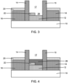
FIGS. 1-6 are cross-sectional views of a structure at successive fabrication stages of a processing method in accordance with embodiments of the invention. -
FIG. 7 is a perspective view of a structure in accordance with alternative embodiments of the invention. - With reference to
FIG. 1 and in accordance with embodiments of the invention, asemiconductor substrate 10 is comprised of a semiconductor material, such as single-crystal silicon. Asemiconductor layer 12 may be formed by patterning thesemiconductor substrate 10 with lithography and etching processes, or by patterning an epitaxially-grown layer. In an embodiment, thesemiconductor layer 12 may be comprised of single-crystal silicon and lack germanium. In an embodiment, thesemiconductor layer 12 may be comprised of single-crystal silicon-germanium that has a uniform germanium concentration. In an embodiment, thesemiconductor layer 12 may be doped (e.g., lightly doped) with a concentration of a p-type dopant (e.g., boron) to provide p-type conductivity. Thesemiconductor layer 12 may provide a portion of an intrinsic base of the bipolar junction transistor. -
Dielectric spacers semiconductor layer 12 by anisotropically etching a deposited conformal dielectric layer. Thedielectric spacers dielectric spacers semiconductor layer 12 as an artifact of the process used to form thesemiconductor layer 12, and acavity 17 exists abovesemiconductor layer 12 and laterally between thedielectric spacer 14 and thedielectric spacer 15. -
Semiconductor layers semiconductor substrate 10 adjacent to the opposite sides of thesemiconductor layer 12. Thesemiconductor layers semiconductor layer 16 may provide an emitter, and thesemiconductor layer 18 may provide a collector. In an alternative embodiment, thesemiconductor layer 16 may provide a collector, and thesemiconductor layer 18 may provide an emitter. - The
semiconductor layers semiconductor layers semiconductor layers - The
dielectric spacer 14 is positioned in a lateral direction between thesemiconductor layer 12 and thesemiconductor layer 16. Thedielectric spacer 15 is positioned in a lateral direction between thesemiconductor layer 12 and thesemiconductor layer 18. Adielectric layer 20 comprised of, for example, silicon nitride may be applied that coats thesemiconductor layers - With reference to
FIG. 2 in which like reference numerals refer to like features inFIG. 1 and at a subsequent fabrication stage, a tilted ion implantation is performed to implant ions, as diagrammatically shown by a single-headed arrow 21, into asection 22 of thesemiconductor layer 12. Thedielectric spacer 15 blocks the implantation of theions 21 into another section of the semiconductor layer 12 (i.e., a non-implanted section that is adjacent to thesection 22 and that is laterally between thesection 22 and the dielectric spacer 15) due to shadowing of the surface area caused by the off-normal incidence of theions 21 during ion implantation. The tilt angle relative to the surface normal is chosen to define the extent of the shadowing by thedielectric spacer 15 and the selectively-implanted volume forming thesection 22. In an embodiment, the tilted ion implantation is performed with thesemiconductor substrate 10 fixed in position. - An unimplanted section of the
semiconductor layer 12 exists following the formation of the implantedsection 22. In an embodiment, the implantedsection 22 may extend from the top surface of thesemiconductor layer 12 partially through thesemiconductor layer 12. In an alternative embodiment, the implantedsection 22 may extend from the top surface of thesemiconductor layer 12 fully through thesemiconductor layer 12. In an embodiment, the implantedsection 22 may include a single atomic layer positioned proximate to the top surface of thesemiconductor layer 12. In an embodiment, the implantedsection 22 may be larger than the unimplanted section of thesemiconductor layer 12. In an embodiment, the implantedsection 22 may be smaller than the unimplanted section of thesemiconductor layer 12. In an embodiment, the implantedsection 22 and the unimplanted section of thesemiconductor layer 12 may have equal sizes. - The implanted
section 22 of thesemiconductor layer 12 is altered to facilitate a subsequent selective etching process in which the implantedsection 22 of thesemiconductor layer 12 has a significantly lower etch rate (i.e., a poisoned surface area). The implantation may change the crystalline structure of the implantedsection 22 of the semiconductor layer 12 (e.g., amorphization) and/or change the material properties of the implantedsection 22 of thesemiconductor layer 12 from those of a semiconductor material to those of, or substantially similar to, a dielectric material. In the latter regard, theions 21 implanted to form the implantedsection 22 may be, or include, gallium, boron, or both elements, and may be performed using a single implantation or multiple implantations. In an embodiment, the concentration of implanted atoms in the implantedsection 22 may be greater than or equal to 1×1019 cm-3. - With reference to
FIG. 3 in which like reference numerals refer to like features inFIG. 2 and at a subsequent fabrication stage, acavity 26 may be formed in thesemiconductor layer 12 by a selective etching process that removes the semiconductor material of the unimplanted section of thesemiconductor layer 12 selective to semiconductor material of the implantedsection 22 of thesemiconductor layer 12. As used herein, the terms "selective" and "selectivity" in reference to a material removal process (e.g., etching) denote that the material removal rate (i.e., etch rate) for the targeted material is higher than the material removal rate (i.e., etch rate) for at least another material exposed to the material removal process. In an embodiment, thecavity 26 may be formed using a wet chemical etching process that employs an etchant solution containing potassium hydroxide. - The etching process is controlled such that the
cavity 26 only penetrates partially through the unimplanted section of thesemiconductor layer 12 in a vertical direction. Thecavity 26 is laterally offset from a vertical centerline of thesemiconductor layer 12 and defines an open space in conjunction with thecavity 17. The implantedsection 22 of thesemiconductor layer 12, which is modified by the implantedions 21, functions as an etch stop such that thecavity 26 is positioned in a lateral direction between the implantedsection 22 and thedielectric spacer 15. - With reference to
FIG. 4 in which like reference numerals refer to like features inFIG. 3 and at a subsequent fabrication stage, asemiconductor layer 28 is formed within thecavity 26 adjacent to the implantedsection 22 of thesemiconductor layer 12, as well within thecavity 17 over thesemiconductor layer 12. Thesemiconductor layer 28 may be comprised of a single-crystal semiconductor material that is epitaxially grown from the exposed surfaces of thesemiconductor layer 12. Thesemiconductor layer 28 includes a portion inside thecavity 17 and a portion inside thecavity 26. In an embodiment, thesemiconductor layer 28 may be comprised of silicon-germanium including silicon and germanium with the silicon content ranging from 95 atomic percent to 50 atomic percent and the germanium content ranging from 5 atomic percent to 50 atomic percent. In an embodiment, the germanium content of thesemiconductor layer 28 may be uniform or substantially uniform over its volume. Thesemiconductor layer 28 may be in situ doped during epitaxial growth with a concentration of a dopant, such as a p-type dopant (e.g., boron) that provides p-type conductivity. In an embodiment, thesemiconductor layer 28 may be uniformly doped during epitaxial growth. Thesemiconductor layer 28, which provides a contribution to the intrinsic base of the bipolar junction transistor, directly contacts the adjacent sections (including the implanted section 22) of thesemiconductor layer 12. - With reference to
FIG. 5 in which like reference numerals refer to like features inFIG. 4 and at a subsequent fabrication stage, a thermal process, such as a rapid thermal anneal, is used to cause germanium to diffuse outwardly from thesemiconductor layer 28 into aportion 30 of thesemiconductor layer 12. Theportion 30 may include all or part of the implantedsection 22. The diffusion of germanium into theportion 30 of thesemiconductor layer 12 may occur in a lateral direction and in a vertical direction. The offset positioning of the portion of thesemiconductor layer 28 inside thecavity 26 adjacent to thesemiconductor layer 18 results in an asymmetrical profile for the germanium that is laterally and vertically diffused into theportion 30 of thesemiconductor layer 12. The thermal process may be controlled such that germanium does not diffuse into a portion of thesemiconductor layer 12 that is positioned between theportion 30 and thesemiconductor substrate 10. The portion of thesemiconductor layer 12 that lacks diffused germanium is positioned adjacent to thesemiconductor substrate 10. - An
interface 31 is defined between theportion 30 of thesemiconductor layer 12 that includes diffused germanium and the portion of thesemiconductor layer 12 that lacks diffused germanium. Although theinterface 31 is diagrammatically shown as inclined inFIG. 5 , theinterface 31 may have a different shape, such as a shape with a degree of curvature or an irregular shape. At and along theinterface 31, the germanium concentration in theportion 30 of thesemiconductor layer 12 has a minimum value and transitions from the germanium concentration in theportion 30 to the germanium concentration, if any, in the portion of thesemiconductor layer 12 that lacks diffused germanium. Theportion 30 of thesemiconductor layer 12 with the multi-directional germanium gradient may extend in a lateral direction from thedielectric spacer 14 to thedielectric spacer 15. - The germanium concentration in the
portion 30 of thesemiconductor layer 12 is graded in a lateral direction and is also graded in a vertical direction. In that regard, the germanium concentration in theportion 30 may decrease with increasing distance from thesemiconductor layer 28 in a lateral direction, and the germanium concentration in theportion 30 may decrease with increasing distance from thesemiconductor layer 28 in a vertical direction. In an embodiment, the germanium concentration in theportion 30 may exhibit a 50 percent decrease per 10 nanometers of distance in a direction from thesemiconductor layer 28 toward theinterface 31. In an embodiment in which thesemiconductor layer 12 is initially comprised of silicon and lacks germanium, the graded germanium profile in theportion 30 of thesemiconductor layer 12 may exhibit a maximum concentration adjacent to the semiconductor layer 18 (e.g., the collector) and a minimum concentration (e.g., 0 atomic percent) at theinterface 31, which is adjacent to the semiconductor layer 16 (e.g., the emitter). In an embodiment in which thesemiconductor layer 12 is initially comprised of silicon-germanium with a uniform or substantially uniform germanium concentration, the minimum germanium concentration at theinterface 31 may be equal to the germanium concentration in the portion ofsemiconductor layer 12 that lacks diffused germanium. The germanium concentration in thesemiconductor layer 28, following the thermal process, may be uniform or substantially uniform and greater than or equal to the maximum germanium concentration in theportion 30 of thesemiconductor layer 12. - With reference to
FIG. 6 in which like reference numerals refer to like features inFIG. 5 and at a subsequent fabrication stage, asemiconductor layer 32 is formed over thesemiconductor layer 28. In an embodiment, thesemiconductor layer 32 may be positioned fully above thesemiconductor layer 28 of the intrinsic base such that the intrinsic base is positioned in a vertical direction between thesemiconductor layer 32 and thesemiconductor substrate 10. Thesemiconductor layer 32 may be comprised of a heavily-doped semiconductor material, such as polysilicon that is heavily doped with a concentration of a p-type dopant (e.g., boron) to provide p-type conductivity. Thesemiconductor layer 32 may provide an extrinsic base of the bipolar junction transistor. - The resultant structure is a lateral bipolar junction transistor that includes a laterallyarranged emitter, base, and collector. The semiconductor layers 16, 18 constitute the emitter and collector of the lateral bipolar junction transistor. The
portion 30 of thesemiconductor layer 12, the portion of thesemiconductor layer 12 that lacks diffused germanium, and thesemiconductor layer 28 may provide different portions of an intrinsic base of the lateral bipolar junction transistor. The germanium concentration in theportion 30 of thesemiconductor layer 12 is graded in a lateral direction between thesemiconductor layer 28 and theinterface 31, and is also graded in a vertical direction between thesemiconductor layer 28 and theinterface 31. In the representative embodiment, the semiconductor layers 16, 18 may contain an n-type dopant, and the semiconductor layers 12, 28, 32 may contain a p-type dopant. In an alternative embodiment, the semiconductor layers 16, 18 may contain a p-type dopant, and the semiconductor layers 12, 28, 32 may contain an n-type dopant. - With reference to
FIG. 7 in which like reference numerals refer to like features inFIG. 6 and in accordance with alternative embodiments, thesemiconductor layer 12 and thesemiconductor layer 28 may constitute afin structure 34 projecting in a vertical direction from thesemiconductor substrate 10. Thefin structure 34 has a width W and a length L that is greater than the width. The lateral grading of the germanium concentration inportion 30 of thesemiconductor layer 12 may extend in a direction along the length of thefin structure 34. In an embodiment, the semiconductor layers 16, 18 may have a faceted shape. - The methods as described above are used in the fabrication of integrated circuit chips. The resulting integrated circuit chips can be distributed by the fabricator in raw wafer form (e.g., as a single wafer that has multiple unpackaged chips), as a bare die, or in a packaged form. The chip may be integrated with other chips, discrete circuit elements, and/or other signal processing devices as part of either an intermediate product or an end product. The end product can be any product that includes integrated circuit chips, such as computer products having a central processor or smartphones.
- References herein to terms modified by language of approximation, such as "about", "approximately", and "substantially", are not to be limited to the precise value specified. The language of approximation may correspond to the precision of an instrument used to measure the value and, unless otherwise dependent on the precision of the instrument, may indicate a range of +/- 10% of the stated value(s).
- References herein to terms such as "vertical", "horizontal", etc. are made by way of example, and not by way of limitation, to establish a frame of reference. The term "horizontal" as used herein is defined as a plane parallel to a conventional plane of a semiconductor substrate, regardless of its actual three-dimensional spatial orientation. The terms "vertical" and "normal" refer to a direction perpendicular to the horizontal, as just defined. The term "lateral" refers to a direction within the horizontal plane.
- A feature "connected" or "coupled" to or with another feature may be directly connected or coupled to or with the other feature or, instead, one or more intervening features may be present. A feature may be "directly connected" or "directly coupled" to or with another feature if intervening features are absent. A feature may be "indirectly connected" or "indirectly coupled" to or with another feature if at least one intervening feature is present. A feature "on" or "contacting" another feature may be directly on or in direct contact with the other feature or, instead, one or more intervening features may be present. A feature may be "directly on" or in "direct contact" with another feature if intervening features are absent. A feature may be "indirectly on" or in "indirect contact" with another feature if at least one intervening feature is present. Different features may "overlap" if a feature extends over, and covers a part of, another feature with either direct contact or indirect contact.
- The descriptions of the various embodiments of the present invention have been presented for purposes of illustration but are not intended to be exhaustive or limited to the embodiments disclosed. Many modifications and variations will be apparent to those of ordinary skill in the art without departing from the scope and spirit of the described embodiments. The terminology used herein was chosen to best explain the principles of the embodiments, the practical application or technical improvement over technologies found in the marketplace, or to enable others of ordinary skill in the art to understand the embodiments disclosed herein.
- The following embodiments are explicitly disclosed:
- A structure for a lateral bipolar junction transistor, the structure comprising:
- a semiconductor substrate;
- a first terminal including a first raised semiconductor layer on the semiconductor substrate;
- a second terminal including a second raised semiconductor layer on the semiconductor substrate; and
- an intrinsic base on the semiconductor substrate, the intrinsic base positioned in a lateral direction between the first raised semiconductor layer of the first terminal and the second raised semiconductor layer of the second terminal, and the intrinsic base including a first portion comprising silicon-germanium with a first germanium concentration that is graded in the lateral direction.
- The structure of embodiment 1 wherein the first germanium concentration in the first portion of the intrinsic base is graded in a vertical direction relative to the semiconductor substrate.
- The structure of embodiment 1 or 2 wherein the intrinsic base is a fin structure projecting in a vertical direction from the semiconductor substrate.
- The structure of embodiment 3 wherein the fin structure has a length and a width, and the grading of the first germanium concentration in the first portion of the intrinsic base extends along the length of the fin structure.
- The structure of one of embodiments 1 to 4 further comprising:
- a first dielectric spacer positioned in the lateral direction between the first raised semiconductor layer and the intrinsic base: and
- a second dielectric spacer positioned in the lateral direction between the second raised semiconductor layer and the intrinsic base,
- wherein the first portion of the intrinsic base extends from the first dielectric spacer to the second dielectric spacer.
- The structure of one of embodiments 1 to 5 wherein the first germanium concentration in the first portion of the intrinsic base decreases in a direction from the first raised semiconductor layer to the second raised semiconductor layer.
- The structure of embodiment 6 wherein the first terminal is an emitter of the lateral bipolar junction transistor, and the second terminal is a collector of the lateral bipolar junction transistor.
- The structure of one of embodiments 1 to 7 wherein the intrinsic base includes a second portion positioned in a vertical direction adjacent to the semiconductor substrate.
- The structure of embodiment 8 wherein the intrinsic base includes a third portion comprising silicon-germanium with a second germanium concentration that is greater than a maximum value of the first germanium concentration, and the first portion of the intrinsic base is positioned in the vertical direction between the third portion of the intrinsic base and the second portion of the intrinsic base.
- The structure of embodiment 9 further comprising:
an extrinsic base on the third portion of the intrinsic base, the extrinsic base comprising a heavily-doped semiconductor material. - The structure of embodiment 8 or 9 wherein the second portion of the intrinsic base comprises silicon-germanium with a second germanium concentration that is substantially uniform and that is less than a minimum value of the first germanium concentration.
- The structure of one of embodiments 8 to 11 to wherein the second portion of the intrinsic base comprises silicon and lacks a germanium concentration.
- The structure of one of embodiments 8 to 13 wherein the first portion of the intrinsic base and the second portion of the intrinsic base adjoin along an interface, and the first germanium concentration has a minimum value at the interface.
- A method of forming a structure for a lateral bipolar junction transistor, the method comprising: forming a first terminal including a first raised semiconductor layer on a semiconductor substrate;
- forming a second terminal including a second raised semiconductor layer on the semiconductor substrate; and
- forming an intrinsic base on the semiconductor substrate that is positioned in a lateral direction between the first raised semiconductor layer of the first terminal and the second raised semiconductor layer of the second terminal,
- wherein the intrinsic base includes a first portion comprising silicon-germanium with a first germanium concentration that is graded in the lateral direction.
- The method of
embodiment 14 wherein the first germanium concentration in the first portion of the intrinsic base is graded in a vertical direction relative to the semiconductor substrate. - The method of
embodiment - depositing a first layer comprised of a first semiconductor material;
- implanting a first section of the first layer; and
- removing a second section of the first layer that is adjacent to the first section to define a cavity.
- The method of
embodiment 16 wherein implanting the first section of the first layer comprises:
performing a tilted implantation of boron or gallium into the first section of the first layer. - The method of
embodiment 17 wherein removing the second section of the first layer that is adjacent to the first section to define the cavity comprises:
performing a wet chemical etching process using an etchant comprising potassium hydroxide. - The method of one of
embodiments 16 to 18 further comprising: - depositing a second layer comprised of a second semiconductor material containing a concentration of germanium, wherein the second layer includes a portion inside the cavity; and
- performing a thermal process to cause the germanium to diffuse in the lateral direction from the second layer into the first layer.
- The method of embodiment 19 wherein the thermal process causes the germanium to diffuse in a vertical direction from the second layer into the first layer.
Claims (15)
- A structure for a lateral bipolar junction transistor, the structure comprising:a semiconductor substrate;a first terminal including a first raised semiconductor layer on the semiconductor substrate;a second terminal including a second raised semiconductor layer on the semiconductor substrate; andan intrinsic base on the semiconductor substrate, the intrinsic base positioned in a lateral direction between the first raised semiconductor layer of the first terminal and the second raised semiconductor layer of the second terminal, and the intrinsic base including a first portion comprising silicon-germanium with a first germanium concentration that is graded in the lateral direction.
- The structure of claim 1, wherein the first germanium concentration in the first portion of the intrinsic base is graded in a vertical direction relative to the semiconductor substrate.
- The structure of claim 1 or 2, wherein the intrinsic base is a fin structure projecting in a vertical direction from the semiconductor substrate, wherein the fin structure preferably has a length and a width, and wherein the grading of the first germanium concentration in the first portion of the intrinsic base preferably extends along the length of the fin structure.
- The structure of one of claims 1 to 3, further comprising:a first dielectric spacer positioned in the lateral direction between the first raised semiconductor layer and the intrinsic base: anda second dielectric spacer positioned in the lateral direction between the second raised semiconductor layer and the intrinsic base,wherein the first portion of the intrinsic base extends from the first dielectric spacer to the second dielectric spacer.
- The structure of one of claims 1 to 4, wherein the first germanium concentration in the first portion of the intrinsic base decreases in a direction from the first raised semiconductor layer to the second raised semiconductor layer.
- The structure of one of claims 1 to 5, wherein the first terminal is an emitter of the lateral bipolar junction transistor, and the second terminal is a collector of the lateral bipolar junction transistor.
- The structure of one of claims 1 to 6, wherein the intrinsic base includes a second portion positioned in a vertical direction adjacent to the semiconductor substrate.
- The structure of claim 7, wherein the intrinsic base includes a third portion comprising silicon-germanium with a second germanium concentration that is greater than a maximum value of the first germanium concentration, and the first portion of the intrinsic base is positioned in the vertical direction between the third portion of the intrinsic base and the second portion of the intrinsic base.
- The structure of claim 8 further comprising:
an extrinsic base on the third portion of the intrinsic base, the extrinsic base comprising a heavily-doped semiconductor material. - The structure of one of claims 7 to 9, wherein the second portion of the intrinsic base comprises silicon-germanium with a second germanium concentration that is substantially uniform and that is less than a minimum value of the first germanium concentration, and/or wherein the second portion of the intrinsic base comprises silicon and lacks a germanium concentration, and/or wherein the first portion of the intrinsic base and the second portion of the intrinsic base adjoin along an interface, and the first germanium concentration has a minimum value at the interface.
- A method of forming a structure for a lateral bipolar junction transistor, the method comprising:forming a first terminal including a first raised semiconductor layer on a semiconductor substrate;forming a second terminal including a second raised semiconductor layer on the semiconductor substrate; andforming an intrinsic base on the semiconductor substrate that is positioned in a lateral direction between the first raised semiconductor layer of the first terminal and the second raised semiconductor layer of the second terminal,wherein the intrinsic base includes a first portion comprising silicon-germanium with a first germanium concentration that is graded in the lateral direction.
- The method of claim 11, wherein the first germanium concentration in the first portion of the intrinsic base is graded in a vertical direction relative to the semiconductor substrate.
- The method of claim 11 or 12, wherein forming the intrinsic base on the semiconductor substrate that is positioned in the lateral direction between the first raised semiconductor layer of the first terminal and the second raised semiconductor layer of the second terminal comprises:depositing a first layer comprised of a first semiconductor material;implanting a first section of the first layer; andremoving a second section of the first layer that is adjacent to the first section to define a cavity.
- The method of claim 13, wherein implanting the first section of the first layer comprises:
performing a tilted implantation of boron or gallium into the first section of the first layer, wherein removing the second section of the first layer that is adjacent to the first section to define the cavity preferably comprises performing a wet chemical etching process using an etchant comprising potassium hydroxide. - The method of claim 13 or 14, further comprising:depositing a second layer comprised of a second semiconductor material containing a concentration of germanium, wherein the second layer includes a portion inside the cavity; andperforming a thermal process to cause the germanium to diffuse in the lateral direction from the second layer into the first layer,wherein the thermal process preferably causes the germanium to diffuse in a vertical direction from the second layer into the first layer.
Applications Claiming Priority (2)
| Application Number | Priority Date | Filing Date | Title |
|---|---|---|---|
| US202263313993P | 2022-02-25 | 2022-02-25 | |
| US17/739,092 US11916136B2 (en) | 2022-02-25 | 2022-05-07 | Lateral bipolar junction transistors including a graded silicon-germanium intrinsic base |
Publications (1)
| Publication Number | Publication Date |
|---|---|
| EP4235795A1 true EP4235795A1 (en) | 2023-08-30 |
Family
ID=83689941
Family Applications (1)
| Application Number | Title | Priority Date | Filing Date |
|---|---|---|---|
| EP22199708.3A Pending EP4235795A1 (en) | 2022-02-25 | 2022-10-05 | Lateral bipolar junction transistors including a graded silicon-germanium intrinsic base |
Country Status (2)
| Country | Link |
|---|---|
| US (1) | US11916136B2 (en) |
| EP (1) | EP4235795A1 (en) |
Cited By (1)
| Publication number | Priority date | Publication date | Assignee | Title |
|---|---|---|---|---|
| EP4586324A1 (en) * | 2024-01-10 | 2025-07-16 | GlobalFoundries U.S. Inc. | Heterojunction bipolar transistors including an intrinsic base with an asymmetrical dopant depth profile |
Citations (6)
| Publication number | Priority date | Publication date | Assignee | Title |
|---|---|---|---|---|
| EP1094523A2 (en) * | 1999-10-21 | 2001-04-25 | Matsushita Electric Industrial Co., Ltd. | Lateral heterojunction bipolar transistor and method of fabricating the same |
| US8288758B2 (en) * | 2010-12-02 | 2012-10-16 | International Business Machines Corporation | SOI SiGe-base lateral bipolar junction transistor |
| US20150263091A1 (en) * | 2014-03-13 | 2015-09-17 | International Business Machines Corporation | LATERAL BIPOLAR JUNCTION TRANSISTOR HAVING GRADED SiGe BASE |
| US9647099B2 (en) * | 2015-04-13 | 2017-05-09 | International Business Machines Corporation | Semiconductor-on-insulator (SOI) lateral heterojunction bipolar transistor having an epitaxially grown base |
| US20180277666A1 (en) * | 2017-03-22 | 2018-09-27 | Taiwan Semiconductor Manufacturing Co., Ltd. | Bipolar junction transistor and integrated circuit device |
| US20210091212A1 (en) * | 2019-09-23 | 2021-03-25 | Globalfoundries U.S. Inc. | Asymmetrical lateral heterojunction bipolar transistors |
Family Cites Families (4)
| Publication number | Priority date | Publication date | Assignee | Title |
|---|---|---|---|---|
| FR2858877B1 (en) | 2003-08-11 | 2005-10-21 | St Microelectronics Sa | BIPOLAR TRANSISTOR WITH HETEROJUNCTION |
| US8227319B2 (en) | 2004-03-10 | 2012-07-24 | Agere Systems Inc. | Bipolar junction transistor having a high germanium concentration in a silicon-germanium layer and a method for forming the bipolar junction transistor |
| US9209095B2 (en) | 2014-04-04 | 2015-12-08 | International Business Machines Corporation | III-V, Ge, or SiGe fin base lateral bipolar transistor structure and method |
| US20190097022A1 (en) | 2017-09-28 | 2019-03-28 | International Business Machine Corporation | Method and structure to form vertical fin bjt with graded sige base doping |
-
2022
- 2022-05-07 US US17/739,092 patent/US11916136B2/en active Active
- 2022-10-05 EP EP22199708.3A patent/EP4235795A1/en active Pending
Patent Citations (6)
| Publication number | Priority date | Publication date | Assignee | Title |
|---|---|---|---|---|
| EP1094523A2 (en) * | 1999-10-21 | 2001-04-25 | Matsushita Electric Industrial Co., Ltd. | Lateral heterojunction bipolar transistor and method of fabricating the same |
| US8288758B2 (en) * | 2010-12-02 | 2012-10-16 | International Business Machines Corporation | SOI SiGe-base lateral bipolar junction transistor |
| US20150263091A1 (en) * | 2014-03-13 | 2015-09-17 | International Business Machines Corporation | LATERAL BIPOLAR JUNCTION TRANSISTOR HAVING GRADED SiGe BASE |
| US9647099B2 (en) * | 2015-04-13 | 2017-05-09 | International Business Machines Corporation | Semiconductor-on-insulator (SOI) lateral heterojunction bipolar transistor having an epitaxially grown base |
| US20180277666A1 (en) * | 2017-03-22 | 2018-09-27 | Taiwan Semiconductor Manufacturing Co., Ltd. | Bipolar junction transistor and integrated circuit device |
| US20210091212A1 (en) * | 2019-09-23 | 2021-03-25 | Globalfoundries U.S. Inc. | Asymmetrical lateral heterojunction bipolar transistors |
Cited By (2)
| Publication number | Priority date | Publication date | Assignee | Title |
|---|---|---|---|---|
| EP4586324A1 (en) * | 2024-01-10 | 2025-07-16 | GlobalFoundries U.S. Inc. | Heterojunction bipolar transistors including an intrinsic base with an asymmetrical dopant depth profile |
| US12690206B2 (en) | 2024-01-10 | 2026-07-21 | Globalfoundries U.S. Inc. | Heterojunction bipolar transistors including an intrinsic base with an asymmetrical dopant depth profile |
Also Published As
| Publication number | Publication date |
|---|---|
| US20230275145A1 (en) | 2023-08-31 |
| US11916136B2 (en) | 2024-02-27 |
Similar Documents
| Publication | Publication Date | Title |
|---|---|---|
| US7750371B2 (en) | Silicon germanium heterojunction bipolar transistor structure and method | |
| US8420493B2 (en) | SOI SiGe-base lateral bipolar junction transistor | |
| US10777668B2 (en) | Bipolar junction transistors with a self-aligned emitter and base | |
| US10115810B2 (en) | Heterojunction bipolar transistor with a thickened extrinsic base | |
| US11063139B2 (en) | Heterojunction bipolar transistors with airgap isolation | |
| US7566921B2 (en) | Silicon germanium emitter | |
| US12501634B2 (en) | Method for forming a transistor with a conductivity doped base structure | |
| US6861324B2 (en) | Method of forming a super self-aligned hetero-junction bipolar transistor | |
| US9053939B2 (en) | Heterojunction bipolar transistor with epitaxial emitter stack to improve vertical scaling | |
| US11916136B2 (en) | Lateral bipolar junction transistors including a graded silicon-germanium intrinsic base | |
| US11888031B2 (en) | Fin-based lateral bipolar junction transistor and method | |
| US8816401B2 (en) | Heterojunction bipolar transistor | |
| US11094805B2 (en) | Lateral heterojunction bipolar transistors with asymmetric junctions | |
| US6531720B2 (en) | Dual sidewall spacer for a self-aligned extrinsic base in SiGe heterojunction bipolar transistors | |
| US10217852B1 (en) | Heterojunction bipolar transistors with a controlled undercut formed beneath the extrinsic base | |
| US10818772B2 (en) | Heterojunction bipolar transistors with an inverted crystalline boundary in the base layer | |
| US10971597B2 (en) | Self-aligned base and emitter for a bipolar junction transistor | |
| US11127843B2 (en) | Asymmetrical lateral heterojunction bipolar transistors | |
| EP4586324A1 (en) | Heterojunction bipolar transistors including an intrinsic base with an asymmetrical dopant depth profile | |
| US12211929B1 (en) | Heterojunction bipolar transistors with terminals having a non-planar arrangement | |
| US11777019B2 (en) | Lateral heterojunction bipolar transistor with improved breakdown voltage and method | |
| KR970004430B1 (en) | Fabrication method of hbt | |
| Narozny et al. | Self aligned Si/SiGe heterojunction bipolar transistors grown by molecular beam epitaxy on diffused n+-buried layer structures |
Legal Events
| Date | Code | Title | Description |
|---|---|---|---|
| PUAI | Public reference made under article 153(3) epc to a published international application that has entered the european phase |
Free format text: ORIGINAL CODE: 0009012 |
|
| STAA | Information on the status of an ep patent application or granted ep patent |
Free format text: STATUS: REQUEST FOR EXAMINATION WAS MADE |
|
| 17P | Request for examination filed |
Effective date: 20221005 |
|
| AK | Designated contracting states |
Kind code of ref document: A1 Designated state(s): AL AT BE BG CH CY CZ DE DK EE ES FI FR GB GR HR HU IE IS IT LI LT LU LV MC ME MK MT NL NO PL PT RO RS SE SI SK SM TR |