EP4235243A1 - Optical components with enhanced heat dissipation - Google Patents
Optical components with enhanced heat dissipation Download PDFInfo
- Publication number
- EP4235243A1 EP4235243A1 EP22200133.1A EP22200133A EP4235243A1 EP 4235243 A1 EP4235243 A1 EP 4235243A1 EP 22200133 A EP22200133 A EP 22200133A EP 4235243 A1 EP4235243 A1 EP 4235243A1
- Authority
- EP
- European Patent Office
- Prior art keywords
- metal feature
- waveguide core
- metallization level
- section
- heat sink
- Prior art date
- Legal status (The legal status is an assumption and is not a legal conclusion. Google has not performed a legal analysis and makes no representation as to the accuracy of the status listed.)
- Granted
Links
Images



Classifications
-
- G—PHYSICS
- G02—OPTICS
- G02B—OPTICAL ELEMENTS, SYSTEMS OR APPARATUS
- G02B6/00—Light guides; Structural details of arrangements comprising light guides and other optical elements, e.g. couplings
- G02B6/10—Light guides; Structural details of arrangements comprising light guides and other optical elements, e.g. couplings of the optical waveguide type
- G02B6/12—Light guides; Structural details of arrangements comprising light guides and other optical elements, e.g. couplings of the optical waveguide type of the integrated circuit kind
- G02B6/122—Basic optical elements, e.g. light-guiding paths
-
- G—PHYSICS
- G02—OPTICS
- G02B—OPTICAL ELEMENTS, SYSTEMS OR APPARATUS
- G02B6/00—Light guides; Structural details of arrangements comprising light guides and other optical elements, e.g. couplings
- G02B6/10—Light guides; Structural details of arrangements comprising light guides and other optical elements, e.g. couplings of the optical waveguide type
- G02B6/12—Light guides; Structural details of arrangements comprising light guides and other optical elements, e.g. couplings of the optical waveguide type of the integrated circuit kind
- G02B6/12002—Three-dimensional structures
-
- G—PHYSICS
- G02—OPTICS
- G02B—OPTICAL ELEMENTS, SYSTEMS OR APPARATUS
- G02B6/00—Light guides; Structural details of arrangements comprising light guides and other optical elements, e.g. couplings
- G02B6/0001—Light guides; Structural details of arrangements comprising light guides and other optical elements, e.g. couplings specially adapted for lighting devices or systems
- G02B6/0011—Light guides; Structural details of arrangements comprising light guides and other optical elements, e.g. couplings specially adapted for lighting devices or systems the light guides being planar or of plate-like form
- G02B6/0013—Means for improving the coupling-in of light from the light source into the light guide
- G02B6/0023—Means for improving the coupling-in of light from the light source into the light guide provided by one optical element, or plurality thereof, placed between the light guide and the light source, or around the light source
- G02B6/0026—Wavelength selective element, sheet or layer, e.g. filter or grating
-
- G—PHYSICS
- G02—OPTICS
- G02B—OPTICAL ELEMENTS, SYSTEMS OR APPARATUS
- G02B6/00—Light guides; Structural details of arrangements comprising light guides and other optical elements, e.g. couplings
- G02B6/24—Coupling light guides
- G02B6/42—Coupling light guides with opto-electronic elements
- G02B6/4201—Packages, e.g. shape, construction, internal or external details
- G02B6/4266—Thermal aspects, temperature control or temperature monitoring
- G02B6/4268—Cooling
- G02B6/4269—Cooling with heat sinks or radiation fins
-
- G—PHYSICS
- G02—OPTICS
- G02B—OPTICAL ELEMENTS, SYSTEMS OR APPARATUS
- G02B6/00—Light guides; Structural details of arrangements comprising light guides and other optical elements, e.g. couplings
- G02B6/24—Coupling light guides
- G02B6/42—Coupling light guides with opto-electronic elements
- G02B6/43—Arrangements comprising a plurality of opto-electronic elements and associated optical interconnections
-
- G—PHYSICS
- G02—OPTICS
- G02B—OPTICAL ELEMENTS, SYSTEMS OR APPARATUS
- G02B6/00—Light guides; Structural details of arrangements comprising light guides and other optical elements, e.g. couplings
- G02B6/10—Light guides; Structural details of arrangements comprising light guides and other optical elements, e.g. couplings of the optical waveguide type
- G02B6/12—Light guides; Structural details of arrangements comprising light guides and other optical elements, e.g. couplings of the optical waveguide type of the integrated circuit kind
- G02B2006/12035—Materials
- G02B2006/12061—Silicon
-
- G—PHYSICS
- G02—OPTICS
- G02B—OPTICAL ELEMENTS, SYSTEMS OR APPARATUS
- G02B6/00—Light guides; Structural details of arrangements comprising light guides and other optical elements, e.g. couplings
- G02B6/10—Light guides; Structural details of arrangements comprising light guides and other optical elements, e.g. couplings of the optical waveguide type
- G02B6/12—Light guides; Structural details of arrangements comprising light guides and other optical elements, e.g. couplings of the optical waveguide type of the integrated circuit kind
- G02B2006/12133—Functions
- G02B2006/12135—Temperature control
-
- G—PHYSICS
- G02—OPTICS
- G02B—OPTICAL ELEMENTS, SYSTEMS OR APPARATUS
- G02B6/00—Light guides; Structural details of arrangements comprising light guides and other optical elements, e.g. couplings
- G02B6/10—Light guides; Structural details of arrangements comprising light guides and other optical elements, e.g. couplings of the optical waveguide type
- G02B6/12—Light guides; Structural details of arrangements comprising light guides and other optical elements, e.g. couplings of the optical waveguide type of the integrated circuit kind
- G02B2006/12133—Functions
- G02B2006/12147—Coupler
-
- G—PHYSICS
- G02—OPTICS
- G02B—OPTICAL ELEMENTS, SYSTEMS OR APPARATUS
- G02B6/00—Light guides; Structural details of arrangements comprising light guides and other optical elements, e.g. couplings
- G02B6/24—Coupling light guides
- G02B6/26—Optical coupling means
- G02B6/30—Optical coupling means for use between fibre and thin-film device
- G02B6/305—Optical coupling means for use between fibre and thin-film device and having an integrated mode-size expanding section, e.g. tapered waveguide
-
- G—PHYSICS
- G02—OPTICS
- G02B—OPTICAL ELEMENTS, SYSTEMS OR APPARATUS
- G02B6/00—Light guides; Structural details of arrangements comprising light guides and other optical elements, e.g. couplings
- G02B6/24—Coupling light guides
- G02B6/42—Coupling light guides with opto-electronic elements
- G02B6/4296—Coupling light guides with opto-electronic elements coupling with sources of high radiant energy, e.g. high power lasers, high temperature light sources
Definitions
- the disclosure relates to photonics chips and, more specifically, to structures including an optical component and methods of fabricating a structure including an optical component.
- Photonics chips are used in many applications and systems including, but not limited to, data communication systems and data computation systems.
- a photonics chip integrates optical components, such as waveguides, photodetectors, modulators, and optical power splitters, and electronic components, such as field-effect transistors, into a unified platform.
- layout area, cost, and operational overhead may be reduced by the integration of both types of components on the same chip.
- An edge coupler also known as a spot-size converter, is commonly used for coupling light of a given mode from a light source, such as a laser or an optical fiber, to optical components on the photonics chip.
- the edge coupler may include a section of a waveguide core that defines an inverse taper having a tip.
- the narrow end of the inverse taper provides a facet at the tip that is positioned adjacent to the light source, and the wide end of the inverse taper is connected with another section of the waveguide core that routes the light to the optical components of the photonics chip.
- the gradually-varying cross-sectional area of the inverse taper supports mode transformation and mode size variation associated with mode conversion when light is transferred from the light source to the edge coupler.
- the tip of the inverse taper is unable to fully confine the incident mode received from the light source because the cross-sectional area of the tip is considerably smaller than the mode size. Consequently, a significant percentage of the electromagnetic field of the incident mode is distributed about the tip of the inverse taper. As its width increases, the inverse taper can support the entire incident mode and confine the electromagnetic field.
- edge couplers may be susceptible to power-related damage because of poor power handling capability, which adversely impacts reliability.
- Particularly susceptive to power-related damage are silicon waveguide cores that are surrounded by low-index cladding containing dielectric materials characterized by poor thermal conductivity.
- non-linear absorption effects in silicon waveguide cores may result in severe thermal heating, and even physical melting, because of an inability to adequately dissipate the generated heat.
- a structure in an embodiment of the invention, includes an optical component, such as a waveguide core or a laser, and a back-end-of-line stack including a first metallization level, a second metallization level, and a heat sink having a metal feature extending through the back-end-of-line stack, for example the first metal feature being in the second metallization level.
- the heat sink is positioned adjacent to the optical component.
- the first metallization level includes a dielectric layer positioned between the metal feature and the section of the waveguide core.
- a structure in an embodiment of the invention, includes a substrate, an optical component, a dielectric layer positioned in a vertical direction between the optical component and the substrate, a back-end-of-line stack on the dielectric layer, and a heat sink including a metal feature extending through the back-end-of-line stack and the dielectric layer to the substrate.
- the metal feature is laterally positioned adjacent to the optical component.
- a method forming a waveguide core, and forming a back-end-of-line stack including a first metallization level, a second metallization level, and a heat sink having a metal feature in the second metallization level.
- the heat sink is positioned adjacent to a section of the waveguide core, and the first metallization level includes a dielectric layer positioned between the metal feature and the section of the waveguide core.
- a structure 10 includes a waveguide core 12 as an optical component.
- the waveguide core 12 may be an edge coupler in which the waveguide core 12 includes an inverse taper 14 and has an end surface defining a facet 16.
- the inverse taper 14 increases in width W1 with increasing distance from the facet 16.
- An inverse taper refers to a tapered section of a waveguide core characterized by a gradual increase in width along a mode propagation direction.
- the waveguide core 12 may be aligned along a longitudinal axis 15, and the waveguide core 12 may have opposite sidewalls 11, 13 that converge at the facet 16.
- the waveguide core 12 may be positioned over a dielectric layer 18 and a substrate 20.
- the dielectric layer 18 may be comprised of a dielectric material, such as silicon dioxide, and the substrate 20 may be comprised of a semiconductor material, such as single-crystal silicon.
- the dielectric layer 18 may be a buried oxide layer of a silicon-on-insulator substrate, and the dielectric layer 18 may separate the waveguide core 12 from the substrate 20.
- the waveguide core 12 may be comprised of a semiconductor material, such as single-crystal silicon.
- the waveguide core 12 may be formed by patterning a single-crystal silicon device layer of a silicon-on-insulator substrate with lithography and etching processes, and the dielectric layer 18 may operate as an etch stop when patterning the waveguide core 12.
- the waveguide core 12 is embodied in a ridge waveguide core. In an alternative embodiment, the waveguide core 12 may be embodied in a rib waveguide core. In an alternative embodiment, the waveguide core 12 may be embodied in a slot waveguide core. In the representative embodiment, the waveguide core 12 is linear or straight. In an alternative embodiment, the waveguide core 12 may be curved. In an alternative embodiment, the waveguide core 12 may be non-tapered. In embodiments, the waveguide core 12 may be part of another optical component such as a polarization mode converter, an optical coupler, a multi-mode interference region, etc.
- a dielectric layer 22 is formed over the waveguide core 12 and dielectric layer 18.
- the dielectric layer 22 may be comprised of a dielectric material, such as silicon dioxide.
- the waveguide core 12 is embedded in the dielectric layer 22.
- a back-end-of-line stack 24 is formed over the dielectric layer 22.
- the back-end-of-line stack 24 may include a metallization level 26, a metallization level 28, and a metallization level 30.
- the metallization level 26 is arranged in a vertical direction between the waveguide core 12 and the metallization level 28.
- the metallization level 28 is arranged in a vertical direction between the metallization level 26 and the metallization level 30.
- the metallization level 26 may include an interlayer dielectric layer 27, the metallization level 28 may include an interlayer dielectric layer 29, and the metallization level 30 may include an interlayer dielectric layer 31.
- the interlayer dielectric layers 27, 29, 31 may be comprised of silicon dioxide.
- a metal feature 32 may be formed in the interlayer dielectric layer 29 of the metallization level 28, a metal feature 34 may be formed in the interlayer dielectric layer 31 of the metallization level 30, and a metal feature 36 may be formed that connects the metal feature 32 to the metal feature 34.
- the metal features 32, 34, 36 which are arranged in a stack, may be positioned to overlap with a section 38 of the waveguide core 12. The overlap is characterized by a portion of each of the metal features 32, 34, 36 being laterally positioned between the sidewalls 11, 13 of the waveguide core 12.
- the section 38 of the waveguide core 12 may be fully overlapped by the metal features 32, 34, 36.
- the section 38 of the waveguide core 12 may have a length in a range of 20 microns to 30 microns.
- the interlayer dielectric layer 27 of the metallization level 26 may be locally free of metal features between the section 38 of the waveguide core 12 and the metal features 32, 34, 36.
- the metallization level 26 may be the closest metallization level of the back-end-of-line stack 24 to the waveguide core 12, and the metallization level 28 may be separated from the waveguide core 12 by only the metallization level 26.
- the metallization level 26 may be the closest metallization level of the back-end-of-line stack 24 to the waveguide core 12, and the dielectric layers of additional metallization levels each locally free of metal features may be positioned between the metallization level 28 and the metallization level 26.
- the metal features 32, 34, 36 are not connected to the waveguide core 12 or the substrate 20, and the metal features 32, 34, 36 are not connected to other metal features in overlying metallization levels (not shown) of the back-end-of-line stack 24.
- the metal features 32, 34, 36 may define a heat sink 40 that is positioned adjacent to the section 38 of the waveguide core 12.
- the metal features 32, 34, 36 may be formed by patterning, deposition, and polishing techniques characteristic of a damascene process. Specifically, the interlayer dielectric layers 27, 29 may be deposited and patterned using lithography and etching processes to define trenches that are filled by a planarized metal (e.g., copper) to define the metal features 32, 34 and to define a via opening that is filled by the metal to define the metal feature 36.
- the metal features 32, 34, 36 may be spaced in a vertical direction from the section 38 of the waveguide core 12 by a spacing S, which may range from about 500 nanometers to about 1 micron.
- the metal feature 32 and the metal feature 36 may have a width W2 that is greater than the width W1 of the section 38 of the waveguide core 12. For example, the width W2 may be equal to 1.5 microns.
- the metal features 32, 34, 36 are linear or straight. In an alternative embodiment, the metal features 32, 34, 36 may be curved. In an alternative embodiment, the waveguide core 12 and the metal features 32, 34, 36 may be curved.
- Light e.g., laser light
- the light may have a given wavelength, intensity, mode shape, and mode size, and the edge coupler providing the representative optical component may provide spot size conversion for the light.
- the light source 60 may be a semiconductor laser, and the semiconductor laser may be positioned inside a cavity formed in the substrate 20 and attached to the substrate 20.
- the structure 10, in any of its embodiments described herein, may be integrated into a photonics chip that includes electronic components and additional optical components.
- the electronic components may include field-effect transistors that are fabricated by CMOS processing.
- the structure 10 provides one or more pathways for heat transfer to cool the waveguide core 12 and thereby reduce the susceptibility of the waveguide core 12 to possible optical power-related damage from, for example, high-power laser light.
- the heat sink 40 efficiently absorbs heat energy generated by light propagating in the waveguide core 12 and conducted as a heat flux through the intervening dielectric material to the metal features 32, 34, 36.
- the heat sink 40 may prevent power-related damage to the section 38 of the waveguide core 12 in the representative embodiment of an edge coupler receiving high-power laser light from the light source 60.
- additional metal features 42, 44, 46 similar to the metal features 32, 34, 36 may be formed in the metallization levels 28, 30 in order to expand the extent of the heat sink 40.
- the set of metal features 32, 34, 36 and the set of metal features 42, 44, 46 may be laterally offset in opposite directions relative to the respective sidewalls 11, 13 of the waveguide core 12.
- the offset 01 of the set of metal features 32, 34, 36 and the offset O2 of the set of metal features 42, 44, 46 may be equal such that the waveguide core 12 is symmetrically positioned between the set of metal features 32, 34, 36 and the set of metal features 42, 44, 46.
- the set of metal features 32, 34, 36 may be offset to have a non-overlapping arrangement with the waveguide core 12, and the set of metal features 42, 44, 46 may also be offset to have a non-overlapping arrangement with the waveguide core 12.
- the offsets 01, O2 may each be less than the width W2 of the metal features 32, 36 and the metal features 42, 46.
- the metal features 32, 34, 36 may be disconnected from the metal features 42, 44, 46.
- the metal features 32, 34, 36 and the metal features 42, 44, 46 are linear or straight. In an alternative embodiment, the metal features 32, 34, 36 and the metal features 42, 44, 46 may be curved. In an alternative embodiment, the waveguide core 12, the metal features 32, 34, 36, and the metal features 42, 44, 46 may be curved.
- the metal features 32, 34, 36 may be connected to metal features in a portion 25a of the back-end-of-line stack 24 that is laterally offset from the waveguide core 12 by a distance greater than the offset 01, and the metal features 42, 44, 46 may be connected to metal features in a portion 25b of the back-end-of-line stack 24 that is laterally offset from the waveguide core 12 by a distance greater than the offset O2.
- the metal feature 36 may be physically connected by a bridging metal feature to a metal feature in the portion 25a of the back-end-of-line stack 24, and the metal feature 46 may be physically connected by a bridging metal feature to a metal feature in the portion 25b of the back-end-of-line stack 24.
- the metal features in the portions 25a, 25b of the back-end-of-line stack 24 may increase the ability of the heat sink 40 to reduce the operating temperature of the section 38 of the waveguide core 12 during use.
- a heat sink 48 may include metal features 50, 52 that are laterally positioned adjacent to the section 38 of the waveguide core 12.
- the metal features 50, 52 are offset in a lateral direction relative to opposite sides of the section 38 of the waveguide core 12.
- the metal features 50, 52 extend in a vertical direction to penetrate through the back-end-of-line stack 24 and the dielectric layer 18 to the substrate 20.
- the metal features 50, 52 may be formed by patterning openings extending through the back-end-of-line stack 24 and the dielectric layer 18 and then filling the openings with a metal (e.g., copper or tungsten).
- the connections of the metal features 50, 52 to the substrate 20 may provide conduction paths that enhance heat transfer away from the section 38 of the waveguide core 12 and thereby improve cooling during operation.
- the optical component represented by the waveguide core 12 may be replaced by a different type of optical component, such as a laser 54, that is located adjacent to the metal features 50, 52.
- the laser 54 may be laterally positioned between the metal feature 50 and the metal feature 52.
- the laser 54 may be disposed inside a cavity that is patterned in the substrate 20.
- the heat sink 48 may receive heat generated by the laser 54 during operation and thereby reduce the operating temperature of the laser 54.
- the methods as described above are used in the fabrication of integrated circuit chips.
- the resulting integrated circuit chips can be distributed by the fabricator in raw wafer form (e.g., as a single wafer that has multiple unpackaged chips), as a bare die, or in a packaged form.
- the chip may be integrated with other chips, discrete circuit elements, and/or other signal processing devices as part of either an intermediate product or an end product.
- the end product can be any product that includes integrated circuit chips, such as computer products having a central processor or smartphones.
- references herein to terms modified by language of approximation, such as “about”, “approximately”, and “substantially”, are not to be limited to the precise value specified.
- the language of approximation may correspond to the precision of an instrument used to measure the value and, unless otherwise dependent on the precision of the instrument, may indicate a range of +/- 10% of the stated value(s).
- references herein to terms such as “vertical”, “horizontal”, etc. are made by way of example, and not by way of limitation, to establish a frame of reference.
- the term “horizontal” as used herein is defined as a plane parallel to a conventional plane of a semiconductor substrate, regardless of its actual three-dimensional spatial orientation.
- the terms “vertical” and “normal” refer to a direction perpendicular to the horizontal, as just defined.
- the term “lateral” refers to a direction within the horizontal plane.
- a feature "connected” or “coupled” to or with another feature may be directly connected or coupled to or with the other feature or, instead, one or more intervening features may be present.
- a feature may be “directly connected” or “directly coupled” to or with another feature if intervening features are absent.
- a feature may be “indirectly connected” or “indirectly coupled” to or with another feature if at least one intervening feature is present.
- a feature “on” or “contacting” another feature may be directly on or in direct contact with the other feature or, instead, one or more intervening features may be present.
- a feature may be “directly on” or in “direct contact” with another feature if intervening features are absent.
- a feature may be “indirectly on” or in “indirect contact” with another feature if at least one intervening feature is present.
- Different features may overlap if a feature extends over, and covers a part of, another feature with either direct contact or indirect contact.
- a structure comprising:
- the section of the waveguide core has a first side surface and a second side surface opposite to the first side surface, the first metal feature is positioned adjacent to the first side surface at a first offset distance, and the second metal feature is positioned adjacent to the second side surface at a second offset distance.
- a structure comprising:
- thermoelectric layer a second metal feature extending through the back-end-of-line stack and the dielectric layer to the substrate, and the second metal feature is laterally positioned adjacent to the optical component.
- a method comprising:
Landscapes
- Physics & Mathematics (AREA)
- General Physics & Mathematics (AREA)
- Optics & Photonics (AREA)
- Engineering & Computer Science (AREA)
- Microelectronics & Electronic Packaging (AREA)
- Optical Integrated Circuits (AREA)
Abstract
Description
- The disclosure relates to photonics chips and, more specifically, to structures including an optical component and methods of fabricating a structure including an optical component.
- Photonics chips are used in many applications and systems including, but not limited to, data communication systems and data computation systems. A photonics chip integrates optical components, such as waveguides, photodetectors, modulators, and optical power splitters, and electronic components, such as field-effect transistors, into a unified platform. Among other factors, layout area, cost, and operational overhead may be reduced by the integration of both types of components on the same chip.
- An edge coupler, also known as a spot-size converter, is commonly used for coupling light of a given mode from a light source, such as a laser or an optical fiber, to optical components on the photonics chip. The edge coupler may include a section of a waveguide core that defines an inverse taper having a tip. In the edge coupler construction, the narrow end of the inverse taper provides a facet at the tip that is positioned adjacent to the light source, and the wide end of the inverse taper is connected with another section of the waveguide core that routes the light to the optical components of the photonics chip.
- The gradually-varying cross-sectional area of the inverse taper supports mode transformation and mode size variation associated with mode conversion when light is transferred from the light source to the edge coupler. The tip of the inverse taper is unable to fully confine the incident mode received from the light source because the cross-sectional area of the tip is considerably smaller than the mode size. Consequently, a significant percentage of the electromagnetic field of the incident mode is distributed about the tip of the inverse taper. As its width increases, the inverse taper can support the entire incident mode and confine the electromagnetic field.
- Conventional edge couplers may be susceptible to power-related damage because of poor power handling capability, which adversely impacts reliability. Particularly susceptive to power-related damage are silicon waveguide cores that are surrounded by low-index cladding containing dielectric materials characterized by poor thermal conductivity. At high optical input powers, non-linear absorption effects in silicon waveguide cores may result in severe thermal heating, and even physical melting, because of an inability to adequately dissipate the generated heat.
- Improved structures including an optical component and methods of fabricating a structure including an optical component are needed.
- In an embodiment of the invention, a structure includes an optical component, such as a waveguide core or a laser, and a back-end-of-line stack including a first metallization level, a second metallization level, and a heat sink having a metal feature extending through the back-end-of-line stack, for example the first metal feature being in the second metallization level. The heat sink is positioned adjacent to the optical component. The first metallization level includes a dielectric layer positioned between the metal feature and the section of the waveguide core.
- In an embodiment of the invention, a structure includes a substrate, an optical component, a dielectric layer positioned in a vertical direction between the optical component and the substrate, a back-end-of-line stack on the dielectric layer, and a heat sink including a metal feature extending through the back-end-of-line stack and the dielectric layer to the substrate. The metal feature is laterally positioned adjacent to the optical component.
- In an embodiment of the invention, a method forming a waveguide core, and forming a back-end-of-line stack including a first metallization level, a second metallization level, and a heat sink having a metal feature in the second metallization level. The heat sink is positioned adjacent to a section of the waveguide core, and the first metallization level includes a dielectric layer positioned between the metal feature and the section of the waveguide core.
- The accompanying drawings, which are incorporated in and constitute a part of this specification, illustrate various embodiments of the invention and, together with a general description of the invention given above and the detailed description of the embodiments given below, serve to explain the embodiments of the invention. In the drawings, like reference numerals refer to like features in the various views.
-
FIG. 1 is a top view of a structure at an initial fabrication stage of a processing method in accordance with embodiments of the invention. -
FIG. 2 is a cross-sectional view of the structure taken generally along line 2-2 inFIG. 1 . -
FIG. 3 is a top view of the structure at a fabrication stage of the processing method subsequent toFIG. 1 . -
FIG. 4 is a cross-sectional view of the structure taken generally along line 4-4 inFIG. 3 . -
FIG. 5 is a top view of a structure in accordance with alternative embodiments of the invention. -
FIG. 6 is a cross-sectional view of the structure taken generally along line 6-6 inFIG. 5 . -
FIG. 7 is a top view of a structure in accordance with alternative embodiments of the invention. -
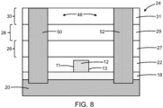
FIG. 8 is a cross-sectional view of a structure in accordance with alternative embodiments of the invention. -
FIG. 9 is a cross-sectional view of a structure in accordance with alternative embodiments of the invention. - With reference to
FIGS. 1, 2 and in accordance with embodiments of the invention, astructure 10 includes awaveguide core 12 as an optical component. In a representative embodiment, thewaveguide core 12 may be an edge coupler in which thewaveguide core 12 includes aninverse taper 14 and has an end surface defining afacet 16. Theinverse taper 14 increases in width W1 with increasing distance from thefacet 16. An inverse taper refers to a tapered section of a waveguide core characterized by a gradual increase in width along a mode propagation direction. Thewaveguide core 12 may be aligned along alongitudinal axis 15, and thewaveguide core 12 may haveopposite sidewalls facet 16. - The
waveguide core 12 may be positioned over adielectric layer 18 and asubstrate 20. In an embodiment, thedielectric layer 18 may be comprised of a dielectric material, such as silicon dioxide, and thesubstrate 20 may be comprised of a semiconductor material, such as single-crystal silicon. In an embodiment, thedielectric layer 18 may be a buried oxide layer of a silicon-on-insulator substrate, and thedielectric layer 18 may separate thewaveguide core 12 from thesubstrate 20. Thewaveguide core 12 may be comprised of a semiconductor material, such as single-crystal silicon. In an embodiment, thewaveguide core 12 may be formed by patterning a single-crystal silicon device layer of a silicon-on-insulator substrate with lithography and etching processes, and thedielectric layer 18 may operate as an etch stop when patterning thewaveguide core 12. - In the representative embodiment, the
waveguide core 12 is embodied in a ridge waveguide core. In an alternative embodiment, thewaveguide core 12 may be embodied in a rib waveguide core. In an alternative embodiment, thewaveguide core 12 may be embodied in a slot waveguide core. In the representative embodiment, thewaveguide core 12 is linear or straight. In an alternative embodiment, thewaveguide core 12 may be curved. In an alternative embodiment, thewaveguide core 12 may be non-tapered. In embodiments, thewaveguide core 12 may be part of another optical component such as a polarization mode converter, an optical coupler, a multi-mode interference region, etc. - With reference to
FIGS. 3 ,4 in which like reference numerals refer to like features inFIGS. 1, 2 and at a subsequent fabrication stage, adielectric layer 22 is formed over thewaveguide core 12 anddielectric layer 18. Thedielectric layer 22 may be comprised of a dielectric material, such as silicon dioxide. Thewaveguide core 12 is embedded in thedielectric layer 22. - A back-end-of-
line stack 24 is formed over thedielectric layer 22. The back-end-of-line stack 24 may include ametallization level 26, ametallization level 28, and ametallization level 30. Themetallization level 26 is arranged in a vertical direction between thewaveguide core 12 and themetallization level 28. Themetallization level 28 is arranged in a vertical direction between themetallization level 26 and themetallization level 30. Themetallization level 26 may include an interlayerdielectric layer 27, themetallization level 28 may include an interlayerdielectric layer 29, and themetallization level 30 may include an interlayerdielectric layer 31. In an embodiment, the interlayerdielectric layers - A
metal feature 32 may be formed in the interlayerdielectric layer 29 of themetallization level 28, ametal feature 34 may be formed in the interlayerdielectric layer 31 of themetallization level 30, and ametal feature 36 may be formed that connects themetal feature 32 to themetal feature 34. The metal features 32, 34, 36, which are arranged in a stack, may be positioned to overlap with asection 38 of thewaveguide core 12. The overlap is characterized by a portion of each of the metal features 32, 34, 36 being laterally positioned between the sidewalls 11, 13 of thewaveguide core 12. In an embodiment, thesection 38 of thewaveguide core 12 may be fully overlapped by the metal features 32, 34, 36. In an embodiment, thesection 38 of thewaveguide core 12 may have a length in a range of 20 microns to 30 microns. - The
interlayer dielectric layer 27 of themetallization level 26 may be locally free of metal features between thesection 38 of thewaveguide core 12 and the metal features 32, 34, 36. In an embodiment, themetallization level 26 may be the closest metallization level of the back-end-of-line stack 24 to thewaveguide core 12, and themetallization level 28 may be separated from thewaveguide core 12 by only themetallization level 26. In an alternative embodiment, themetallization level 26 may be the closest metallization level of the back-end-of-line stack 24 to thewaveguide core 12, and the dielectric layers of additional metallization levels each locally free of metal features may be positioned between themetallization level 28 and themetallization level 26. In an embodiment, the metal features 32, 34, 36 are not connected to thewaveguide core 12 or thesubstrate 20, and the metal features 32, 34, 36 are not connected to other metal features in overlying metallization levels (not shown) of the back-end-of-line stack 24. - The metal features 32, 34, 36 may define a
heat sink 40 that is positioned adjacent to thesection 38 of thewaveguide core 12. The metal features 32, 34, 36 may be formed by patterning, deposition, and polishing techniques characteristic of a damascene process. Specifically, the interlayer dielectric layers 27, 29 may be deposited and patterned using lithography and etching processes to define trenches that are filled by a planarized metal (e.g., copper) to define the metal features 32, 34 and to define a via opening that is filled by the metal to define themetal feature 36. In an embodiment, the metal features 32, 34, 36 may be spaced in a vertical direction from thesection 38 of thewaveguide core 12 by a spacing S, which may range from about 500 nanometers to about 1 micron. In an embodiment, themetal feature 32 and themetal feature 36 may have a width W2 that is greater than the width W1 of thesection 38 of thewaveguide core 12. For example, the width W2 may be equal to 1.5 microns. - In the representative embodiment, the metal features 32, 34, 36 are linear or straight. In an alternative embodiment, the metal features 32, 34, 36 may be curved. In an alternative embodiment, the
waveguide core 12 and the metal features 32, 34, 36 may be curved. - Light (e.g., laser light) may be directed from a
light source 60 toward thefacet 16 of thewaveguide core 12. The light may have a given wavelength, intensity, mode shape, and mode size, and the edge coupler providing the representative optical component may provide spot size conversion for the light. In an embodiment, thelight source 60 may be a semiconductor laser, and the semiconductor laser may be positioned inside a cavity formed in thesubstrate 20 and attached to thesubstrate 20. - The
structure 10, in any of its embodiments described herein, may be integrated into a photonics chip that includes electronic components and additional optical components. For example, the electronic components may include field-effect transistors that are fabricated by CMOS processing. - The
structure 10 provides one or more pathways for heat transfer to cool thewaveguide core 12 and thereby reduce the susceptibility of thewaveguide core 12 to possible optical power-related damage from, for example, high-power laser light. In particular, theheat sink 40 efficiently absorbs heat energy generated by light propagating in thewaveguide core 12 and conducted as a heat flux through the intervening dielectric material to the metal features 32, 34, 36. For example, theheat sink 40 may prevent power-related damage to thesection 38 of thewaveguide core 12 in the representative embodiment of an edge coupler receiving high-power laser light from thelight source 60. - With reference to
FIGS. 5 ,6 and in accordance with alternative embodiments of the invention, additional metal features 42, 44, 46 similar to the metal features 32, 34, 36 may be formed in themetallization levels heat sink 40. In an embodiment, the set of metal features 32, 34, 36 and the set of metal features 42, 44, 46 may be laterally offset in opposite directions relative to therespective sidewalls waveguide core 12. In an embodiment, the offset 01 of the set of metal features 32, 34, 36 and the offset O2 of the set of metal features 42, 44, 46 may be equal such that thewaveguide core 12 is symmetrically positioned between the set of metal features 32, 34, 36 and the set of metal features 42, 44, 46. In an embodiment, the set of metal features 32, 34, 36 may be offset to have a non-overlapping arrangement with thewaveguide core 12, and the set of metal features 42, 44, 46 may also be offset to have a non-overlapping arrangement with thewaveguide core 12. In an embodiment, theoffsets 01, O2 may each be less than the width W2 of the metal features 32, 36 and the metal features 42, 46. In an embodiment, the metal features 32, 34, 36 may be disconnected from the metal features 42, 44, 46. - In the representative embodiment, the metal features 32, 34, 36 and the metal features 42, 44, 46 are linear or straight. In an alternative embodiment, the metal features 32, 34, 36 and the metal features 42, 44, 46 may be curved. In an alternative embodiment, the
waveguide core 12, the metal features 32, 34, 36, and the metal features 42, 44, 46 may be curved. - With reference to
FIG. 7 and in accordance with alternative embodiments of the invention, the metal features 32, 34, 36 may be connected to metal features in aportion 25a of the back-end-of-line stack 24 that is laterally offset from thewaveguide core 12 by a distance greater than the offset 01, and the metal features 42, 44, 46 may be connected to metal features in aportion 25b of the back-end-of-line stack 24 that is laterally offset from thewaveguide core 12 by a distance greater than the offset O2. For example, themetal feature 36 may be physically connected by a bridging metal feature to a metal feature in theportion 25a of the back-end-of-line stack 24, and themetal feature 46 may be physically connected by a bridging metal feature to a metal feature in theportion 25b of the back-end-of-line stack 24. The metal features in theportions line stack 24 may increase the ability of theheat sink 40 to reduce the operating temperature of thesection 38 of thewaveguide core 12 during use. - With reference to
FIG. 8 and in accordance with alternative embodiments of the invention, aheat sink 48 may include metal features 50, 52 that are laterally positioned adjacent to thesection 38 of thewaveguide core 12. The metal features 50, 52 are offset in a lateral direction relative to opposite sides of thesection 38 of thewaveguide core 12. The metal features 50, 52 extend in a vertical direction to penetrate through the back-end-of-line stack 24 and thedielectric layer 18 to thesubstrate 20. The metal features 50, 52 may be formed by patterning openings extending through the back-end-of-line stack 24 and thedielectric layer 18 and then filling the openings with a metal (e.g., copper or tungsten). The connections of the metal features 50, 52 to thesubstrate 20 may provide conduction paths that enhance heat transfer away from thesection 38 of thewaveguide core 12 and thereby improve cooling during operation. - With reference to
FIG. 9 and in accordance with alternative embodiments of the invention, the optical component represented by thewaveguide core 12 may be replaced by a different type of optical component, such as alaser 54, that is located adjacent to the metal features 50, 52. In an embodiment, thelaser 54 may be laterally positioned between themetal feature 50 and themetal feature 52. Thelaser 54 may be disposed inside a cavity that is patterned in thesubstrate 20. Theheat sink 48 may receive heat generated by thelaser 54 during operation and thereby reduce the operating temperature of thelaser 54. - The methods as described above are used in the fabrication of integrated circuit chips. The resulting integrated circuit chips can be distributed by the fabricator in raw wafer form (e.g., as a single wafer that has multiple unpackaged chips), as a bare die, or in a packaged form. The chip may be integrated with other chips, discrete circuit elements, and/or other signal processing devices as part of either an intermediate product or an end product. The end product can be any product that includes integrated circuit chips, such as computer products having a central processor or smartphones.
- References herein to terms modified by language of approximation, such as "about", "approximately", and "substantially", are not to be limited to the precise value specified. The language of approximation may correspond to the precision of an instrument used to measure the value and, unless otherwise dependent on the precision of the instrument, may indicate a range of +/- 10% of the stated value(s).
- References herein to terms such as "vertical", "horizontal", etc. are made by way of example, and not by way of limitation, to establish a frame of reference. The term "horizontal" as used herein is defined as a plane parallel to a conventional plane of a semiconductor substrate, regardless of its actual three-dimensional spatial orientation. The terms "vertical" and "normal" refer to a direction perpendicular to the horizontal, as just defined. The term "lateral" refers to a direction within the horizontal plane.
- A feature "connected" or "coupled" to or with another feature may be directly connected or coupled to or with the other feature or, instead, one or more intervening features may be present. A feature may be "directly connected" or "directly coupled" to or with another feature if intervening features are absent. A feature may be "indirectly connected" or "indirectly coupled" to or with another feature if at least one intervening feature is present. A feature "on" or "contacting" another feature may be directly on or in direct contact with the other feature or, instead, one or more intervening features may be present. A feature may be "directly on" or in "direct contact" with another feature if intervening features are absent. A feature may be "indirectly on" or in "indirect contact" with another feature if at least one intervening feature is present. Different features may overlap if a feature extends over, and covers a part of, another feature with either direct contact or indirect contact.
- The descriptions of the various embodiments of the present invention have been presented for purposes of illustration but are not intended to be exhaustive or limited to the embodiments disclosed. Many modifications and variations will be apparent to those of ordinary skill in the art without departing from the scope and spirit of the described embodiments. The terminology used herein was chosen to best explain the principles of the embodiments, the practical application or technical improvement over technologies found in the marketplace, or to enable others of ordinary skill in the art to understand the embodiments disclosed herein.
- The following embodiments are explicitly disclosred:
- A structure comprising:
- a waveguide core including a section; and
- a back-end-of-line stack including a first metallization level, a second metallization level, and a heat sink having a first metal feature in the second metallization level, the heat sink positioned adjacent to the section of the waveguide core, and the first metallization level including a dielectric layer positioned between the first metal feature and the section of the waveguide core.
- The structure of embodiment 1, wherein the waveguide core comprises an edge coupler having a facet, and the heat sink is positioned adjacent to the facet.
- The structure of
embodiment 1 or 2, wherein the back-end-of-line stack includes a third metallization level, the second metallization level is positioned between the third metallization level and the first metallization level, and the heat sink includes a second metal feature in the third metallization level. - The structure of embodiment 3, wherein the heat sink includes a third metal feature that connects the first metal feature to the second metal feature.
- The structure of one of embodiments 1 to 4, wherein the first metal feature is positioned to overlap with the section of the waveguide core.
- The structure of one of embodiments 1 to 5, wherein the first metal feature is laterally offset relative to the section of the waveguide core such that the first metal feature has a non-overlapping relationship with the section of the waveguide core.
- The structure of one of embodiments 1 to 6, wherein the heat sink including a second metal feature in the second metallization level, and the first metal feature and the second metal feature of the heat sink are laterally offset relative to the section of the waveguide core such that the first metal feature and the second metal feature have respective non-overlapping relationships with the section of the waveguide core.
- The structure of embodiment 7, wherein the section of the waveguide core has a first side surface and a second side surface opposite to the first side surface, the first metal feature is positioned adjacent to the first side surface at a first offset distance, and the second metal feature is positioned adjacent to the second side surface at a second offset distance.
- The structure of embodiment 8, wherein the first offset distance is equal to the second offset distance.
- The structure of one of embodiments 7 to 9, wherein the first metal feature is not connected to the second metal feature.
- The structure of one of embodiments 1 to 10, wherein the waveguide core comprises silicon.
- A structure comprising:
- a substrate;
- an optical component;
- a dielectric layer positioned in a vertical direction between the optical component and the substrate;
- a back-end-of-line stack on the dielectric layer; and
- a heat sink including a first metal feature extending through the back-end-of-line stack and the dielectric layer to the substrate, the first metal feature laterally positioned adjacent to the optical component.
- The structure of
embodiment 12, wherein the optical component is a laser. - The structure of
embodiment - The structure of one of
embodiments 12 to 14, wherein the heat sink includes a second metal feature extending through the back-end-of-line stack and the dielectric layer to the substrate, and the second metal feature is laterally positioned adjacent to the optical component. - The structure of
embodiment 15, wherein the optical component is laterally positioned between the first metal feature and the second metal feature. - A method comprising:
- forming a waveguide core; and
- forming a back-end-of-line stack including a first metallization level, a second metallization level, and a heat sink having a first metal feature in the second metallization level,
- wherein the heat sink is positioned adjacent to a section of the waveguide core, and the first metallization level includes a dielectric layer positioned between the first metal feature and the section of the waveguide core.
- The method of embodiment 17, wherein the back-end-of-line stack includes a third metallization level, the second metallization level is positioned between the third metallization level and the first metallization level, and the heat sink includes a second metal feature formed in the third metallization level.
- The method of
embodiment 17 or 18, wherein the first metal feature is positioned to overlap with the section of the waveguide core. - The method of one of embodiments 17 to 19, wherein the first metal feature is laterally offset relative to the section of the waveguide core such that the first metal feature has a non-overlapping relationship with the section of the waveguide core.
Claims (14)
- A structure comprising:an optical component; anda back-end-of-line stack including a first metallization level, a second metallization level, and a heat sink having a first metal feature extending through the back-end-of-line stack, preferably the first metal feature being in the second metallization level, the heat sink positioned adjacent to the optical component, preferably adjacent to the section of the waveguide core, and the first metallization level including a dielectric layer positioned between the first metal feature and the section of the waveguide core.
- The structure of claim 1, wherein the optical component is one of a waveguide core including a section, wherein the waveguide core preferably comprises silicon, and a laser.
- The structure of claim 1 or 2, wherein the optical component comprises an edge coupler having a facet, and the heat sink is positioned adjacent to the facet.
- The structure of one of claims 1 to 3, wherein the back-end-of-line stack includes a third metallization level, the second metallization level is positioned between the third metallization level and the first metallization level, and the heat sink includes a second metal feature in the third metallization level, the heat sink preferably including a third metal feature that connects the first metal feature to the second metal feature.
- The structure of one of claims 1 to 4, wherein the optical component is a waveguide core including a section and the first metal feature is positioned to overlap with the section of the waveguide core, and/or wherein the first metal feature is laterally offset relative to the section of the waveguide core such that the first metal feature has a non-overlapping relationship with the section of the waveguide core.
- The structure of one of claims 1 to 5, wherein the optical component is a waveguide core including a section, and wherein the heat sink including a second metal feature in the second metallization level, and the first metal feature and the second metal feature of the heat sink are laterally offset relative to the section of the waveguide core such that the first metal feature and the second metal feature have respective non-overlapping relationships with the section of the waveguide core.
- The structure of claim 6, wherein the section of the waveguide core has a first side surface and a second side surface opposite to the first side surface, the first metal feature is positioned adjacent to the first side surface at a first offset distance, and the second metal feature is positioned adjacent to the second side surface at a second offset distance, the first offset distance preferably being equal to the second offset distance, and/or wherein the first metal feature is not connected to the second metal feature.
- The structure of one of claims 1 to 7, further comprising a substrate, the dielectric layer being positioned in a vertical direction between the optical component and the substrate, and the heat sink including the first metal feature extending through the back-end-of-line stack and the dielectric layer to the substrate, the first metal feature laterally positioned adjacent to the optical component.
- The structure of claim 8, wherein the heat sink includes a second metal feature extending through the back-end-of-line stack and the dielectric layer to the substrate, and the second metal feature is laterally positioned adjacent to the optical component.
- The structure of claim 8 or 9, wherein the optical component is laterally positioned between the first metal feature and the second metal feature.
- A method comprising:forming a waveguide core; andforming a back-end-of-line stack including a first metallization level, a second metallization level, and a heat sink having a first metal feature in the second metallization level,wherein the heat sink is positioned adjacent to a section of the waveguide core, and the first metallization level includes a dielectric layer positioned between the first metal feature and the section of the waveguide core.
- The method of claim 11, wherein the back-end-of-line stack includes a third metallization level, the second metallization level is positioned between the third metallization level and the first metallization level, and the heat sink includes a second metal feature formed in the third metallization level.
- The method of claim 11 or 12, wherein the first metal feature is positioned to overlap with the section of the waveguide core.
- The method of one of claims 11 to 13, wherein the first metal feature is laterally offset relative to the section of the waveguide core such that the first metal feature has a non-overlapping relationship with the section of the waveguide core.
Applications Claiming Priority (1)
| Application Number | Priority Date | Filing Date | Title |
|---|---|---|---|
| US17/679,405 US11822120B2 (en) | 2022-02-24 | 2022-02-24 | Optical components with enhanced heat dissipation |
Publications (3)
| Publication Number | Publication Date |
|---|---|
| EP4235243A1 true EP4235243A1 (en) | 2023-08-30 |
| EP4235243B1 EP4235243B1 (en) | 2025-09-03 |
| EP4235243C0 EP4235243C0 (en) | 2025-09-03 |
Family
ID=83688907
Family Applications (1)
| Application Number | Title | Priority Date | Filing Date |
|---|---|---|---|
| EP22200133.1A Active EP4235243B1 (en) | 2022-02-24 | 2022-10-06 | Optical components with enhanced heat dissipation |
Country Status (2)
| Country | Link |
|---|---|
| US (1) | US11822120B2 (en) |
| EP (1) | EP4235243B1 (en) |
Families Citing this family (4)
| Publication number | Priority date | Publication date | Assignee | Title |
|---|---|---|---|---|
| US11846804B2 (en) | 2022-02-24 | 2023-12-19 | Globalfoundries U.S. Inc. | Thermally-conductive features positioned adjacent to an optical component |
| US20230019747A1 (en) * | 2022-09-23 | 2023-01-19 | Richard Jones | Hybrid laser architecture with asymmetric metal shunt |
| US20260003120A1 (en) * | 2024-07-01 | 2026-01-01 | Globalfoundries U.S. Inc. | Optical signal blockers for a photonic chip |
| EP4726463A1 (en) * | 2024-10-08 | 2026-04-15 | Université Grenoble Alpes | Reconfigurable photonic device |
Citations (2)
| Publication number | Priority date | Publication date | Assignee | Title |
|---|---|---|---|---|
| US20160363728A1 (en) * | 2015-06-12 | 2016-12-15 | Pacific Biosciences Of California, Inc. | Integrated target waveguide devices and systems for optical coupling |
| US20170371099A1 (en) * | 2013-06-24 | 2017-12-28 | Stmicroelectronics Sa | Methods of Fabricating Integrated Circuit Devices With Components on Both Sides of a Semiconductor Layer and the Devices Formed Thereby |
Family Cites Families (6)
| Publication number | Priority date | Publication date | Assignee | Title |
|---|---|---|---|---|
| US6847748B2 (en) | 2002-10-15 | 2005-01-25 | Xponent Photonics Inc | Heat sink for a planar waveguide substrate |
| JP4634897B2 (en) | 2005-09-12 | 2011-02-16 | 日本電信電話株式会社 | Multi-channel waveguide-type thermo-optic variable attenuator and manufacturing method thereof |
| US9064080B2 (en) * | 2011-01-20 | 2015-06-23 | International Business Machines Corporation | Transferring heat through an optical layer of integrated circuitry |
| WO2014042637A1 (en) * | 2012-09-13 | 2014-03-20 | Hewlett-Packard Development Company, L.P. | Controlling temperatures in optical circuits |
| JP6636903B2 (en) | 2016-12-05 | 2020-01-29 | 日本電信電話株式会社 | Optical components |
| US10283931B2 (en) * | 2017-05-05 | 2019-05-07 | International Business Machines Corporation | Electro-optical device with III-V gain materials and integrated heat sink |
-
2022
- 2022-02-24 US US17/679,405 patent/US11822120B2/en active Active
- 2022-10-06 EP EP22200133.1A patent/EP4235243B1/en active Active
Patent Citations (2)
| Publication number | Priority date | Publication date | Assignee | Title |
|---|---|---|---|---|
| US20170371099A1 (en) * | 2013-06-24 | 2017-12-28 | Stmicroelectronics Sa | Methods of Fabricating Integrated Circuit Devices With Components on Both Sides of a Semiconductor Layer and the Devices Formed Thereby |
| US20160363728A1 (en) * | 2015-06-12 | 2016-12-15 | Pacific Biosciences Of California, Inc. | Integrated target waveguide devices and systems for optical coupling |
Also Published As
| Publication number | Publication date |
|---|---|
| US20230266529A1 (en) | 2023-08-24 |
| EP4235243B1 (en) | 2025-09-03 |
| EP4235243C0 (en) | 2025-09-03 |
| US11822120B2 (en) | 2023-11-21 |
Similar Documents
| Publication | Publication Date | Title |
|---|---|---|
| US11822120B2 (en) | Optical components with enhanced heat dissipation | |
| US11531164B2 (en) | Hybrid edge couplers with layers in multiple levels | |
| US11366269B2 (en) | Edge couplers with a partially-etched inverse taper | |
| US7113676B2 (en) | Planar waveguide optical isolator in thin silicon-on-isolator (SOI) structure | |
| US12174420B2 (en) | Thermally-conductive features positioned adjacent to an optical component | |
| US9093428B2 (en) | Thermal shunt | |
| CN104395797B (en) | The method and apparatus of PHOTONIC DEVICE being thermally isolated is provided | |
| US11536903B1 (en) | Hybrid edge couplers with stacked inverse tapers | |
| US20150318665A1 (en) | Thermal Shunt | |
| US12444906B2 (en) | Heterogeneously integrated photonic platform with improved thermal performance | |
| US11137543B2 (en) | Polarizers with an absorber | |
| CN115113326B (en) | Optical coupler for ridge-to-rib waveguide core transition | |
| CN114488393A (en) | Optical power splitter with multi-level arrangement | |
| US12117648B2 (en) | Hybrid integration method | |
| CN116643336B (en) | Thermal management of optical components for temperature control | |
| EP4398010A1 (en) | Edge couplers with a fine-alignment mechanism | |
| EP4235242B1 (en) | Spot-size converters with angled facets | |
| US12050348B2 (en) | Fiber to chip coupler and method of making the same | |
| US12541059B2 (en) | Managing back-side processing of photonic integrated circuits |
Legal Events
| Date | Code | Title | Description |
|---|---|---|---|
| PUAI | Public reference made under article 153(3) epc to a published international application that has entered the european phase |
Free format text: ORIGINAL CODE: 0009012 |
|
| STAA | Information on the status of an ep patent application or granted ep patent |
Free format text: STATUS: REQUEST FOR EXAMINATION WAS MADE |
|
| 17P | Request for examination filed |
Effective date: 20221006 |
|
| AK | Designated contracting states |
Kind code of ref document: A1 Designated state(s): AL AT BE BG CH CY CZ DE DK EE ES FI FR GB GR HR HU IE IS IT LI LT LU LV MC ME MK MT NL NO PL PT RO RS SE SI SK SM TR |
|
| GRAP | Despatch of communication of intention to grant a patent |
Free format text: ORIGINAL CODE: EPIDOSNIGR1 |
|
| STAA | Information on the status of an ep patent application or granted ep patent |
Free format text: STATUS: GRANT OF PATENT IS INTENDED |
|
| RIC1 | Information provided on ipc code assigned before grant |
Ipc: G02B 6/30 20060101ALN20250521BHEP Ipc: H01L 23/367 20060101ALI20250521BHEP Ipc: G02B 6/12 20060101ALI20250521BHEP Ipc: G02B 6/42 20060101AFI20250521BHEP |
|
| INTG | Intention to grant announced |
Effective date: 20250604 |
|
| GRAS | Grant fee paid |
Free format text: ORIGINAL CODE: EPIDOSNIGR3 |
|
| GRAA | (expected) grant |
Free format text: ORIGINAL CODE: 0009210 |
|
| STAA | Information on the status of an ep patent application or granted ep patent |
Free format text: STATUS: THE PATENT HAS BEEN GRANTED |
|
| AK | Designated contracting states |
Kind code of ref document: B1 Designated state(s): AL AT BE BG CH CY CZ DE DK EE ES FI FR GB GR HR HU IE IS IT LI LT LU LV MC ME MK MT NL NO PL PT RO RS SE SI SK SM TR |
|
| REG | Reference to a national code |
Ref country code: CH Ref legal event code: EP |
|
| REG | Reference to a national code |
Ref country code: DE Ref legal event code: R096 Ref document number: 602022020640 Country of ref document: DE |
|
| REG | Reference to a national code |
Ref country code: IE Ref legal event code: FG4D |
|
| U01 | Request for unitary effect filed |
Effective date: 20250926 |
|
| U07 | Unitary effect registered |
Designated state(s): AT BE BG DE DK EE FI FR IT LT LU LV MT NL PT RO SE SI Effective date: 20251007 |
|
| U20 | Renewal fee for the european patent with unitary effect paid |
Year of fee payment: 4 Effective date: 20251118 |
|
| PG25 | Lapsed in a contracting state [announced via postgrant information from national office to epo] |
Ref country code: NO Free format text: LAPSE BECAUSE OF FAILURE TO SUBMIT A TRANSLATION OF THE DESCRIPTION OR TO PAY THE FEE WITHIN THE PRESCRIBED TIME-LIMIT Effective date: 20251203 |
|
| PG25 | Lapsed in a contracting state [announced via postgrant information from national office to epo] |
Ref country code: HR Free format text: LAPSE BECAUSE OF FAILURE TO SUBMIT A TRANSLATION OF THE DESCRIPTION OR TO PAY THE FEE WITHIN THE PRESCRIBED TIME-LIMIT Effective date: 20250903 |
|
| PG25 | Lapsed in a contracting state [announced via postgrant information from national office to epo] |
Ref country code: GR Free format text: LAPSE BECAUSE OF FAILURE TO SUBMIT A TRANSLATION OF THE DESCRIPTION OR TO PAY THE FEE WITHIN THE PRESCRIBED TIME-LIMIT Effective date: 20251204 |
|
| PG25 | Lapsed in a contracting state [announced via postgrant information from national office to epo] |
Ref country code: PL Free format text: LAPSE BECAUSE OF FAILURE TO SUBMIT A TRANSLATION OF THE DESCRIPTION OR TO PAY THE FEE WITHIN THE PRESCRIBED TIME-LIMIT Effective date: 20250903 |
|
| PG25 | Lapsed in a contracting state [announced via postgrant information from national office to epo] |
Ref country code: RS Free format text: LAPSE BECAUSE OF FAILURE TO SUBMIT A TRANSLATION OF THE DESCRIPTION OR TO PAY THE FEE WITHIN THE PRESCRIBED TIME-LIMIT Effective date: 20251203 |
|
| PG25 | Lapsed in a contracting state [announced via postgrant information from national office to epo] |
Ref country code: ES Free format text: LAPSE BECAUSE OF FAILURE TO SUBMIT A TRANSLATION OF THE DESCRIPTION OR TO PAY THE FEE WITHIN THE PRESCRIBED TIME-LIMIT Effective date: 20250903 |
|
| PG25 | Lapsed in a contracting state [announced via postgrant information from national office to epo] |
Ref country code: SM Free format text: LAPSE BECAUSE OF FAILURE TO SUBMIT A TRANSLATION OF THE DESCRIPTION OR TO PAY THE FEE WITHIN THE PRESCRIBED TIME-LIMIT Effective date: 20250903 |
|
| PG25 | Lapsed in a contracting state [announced via postgrant information from national office to epo] |
Ref country code: IS Free format text: LAPSE BECAUSE OF FAILURE TO SUBMIT A TRANSLATION OF THE DESCRIPTION OR TO PAY THE FEE WITHIN THE PRESCRIBED TIME-LIMIT Effective date: 20260103 |
|
| PG25 | Lapsed in a contracting state [announced via postgrant information from national office to epo] |
Ref country code: CZ Free format text: LAPSE BECAUSE OF FAILURE TO SUBMIT A TRANSLATION OF THE DESCRIPTION OR TO PAY THE FEE WITHIN THE PRESCRIBED TIME-LIMIT Effective date: 20250903 |
|
| PG25 | Lapsed in a contracting state [announced via postgrant information from national office to epo] |
Ref country code: SK Free format text: LAPSE BECAUSE OF FAILURE TO SUBMIT A TRANSLATION OF THE DESCRIPTION OR TO PAY THE FEE WITHIN THE PRESCRIBED TIME-LIMIT Effective date: 20250903 |
|
| REG | Reference to a national code |
Ref country code: CH Ref legal event code: H13 Free format text: ST27 STATUS EVENT CODE: U-0-0-H10-H13 (AS PROVIDED BY THE NATIONAL OFFICE) Effective date: 20260527 |
|
| PG25 | Lapsed in a contracting state [announced via postgrant information from national office to epo] |
Ref country code: MC Free format text: LAPSE BECAUSE OF FAILURE TO SUBMIT A TRANSLATION OF THE DESCRIPTION OR TO PAY THE FEE WITHIN THE PRESCRIBED TIME-LIMIT Effective date: 20250903 |
|
| PLBE | No opposition filed within time limit |
Free format text: ORIGINAL CODE: 0009261 |
|
| STAA | Information on the status of an ep patent application or granted ep patent |
Free format text: STATUS: NO OPPOSITION FILED WITHIN TIME LIMIT |
|
| REG | Reference to a national code |
Ref country code: CH Ref legal event code: L10 Free format text: ST27 STATUS EVENT CODE: U-0-0-L10-L00 (AS PROVIDED BY THE NATIONAL OFFICE) Effective date: 20260715 |
|
| PG25 | Lapsed in a contracting state [announced via postgrant information from national office to epo] |
Ref country code: CH Free format text: LAPSE BECAUSE OF NON-PAYMENT OF DUE FEES Effective date: 20251031 |
|
| 26N | No opposition filed |
Effective date: 20260604 |