EP4235191A1 - Contact probe - Google Patents
Contact probe Download PDFInfo
- Publication number
- EP4235191A1 EP4235191A1 EP21882624.6A EP21882624A EP4235191A1 EP 4235191 A1 EP4235191 A1 EP 4235191A1 EP 21882624 A EP21882624 A EP 21882624A EP 4235191 A1 EP4235191 A1 EP 4235191A1
- Authority
- EP
- European Patent Office
- Prior art keywords
- plunger
- tip portion
- contact probe
- contact
- projection
- Prior art date
- Legal status (The legal status is an assumption and is not a legal conclusion. Google has not performed a legal analysis and makes no representation as to the accuracy of the status listed.)
- Withdrawn
Links
- 239000000523 sample Substances 0.000 title claims abstract description 37
- 239000007769 metal material Substances 0.000 claims abstract description 22
- 238000007689 inspection Methods 0.000 claims description 28
- 239000000463 material Substances 0.000 claims description 28
- 229910001252 Pd alloy Inorganic materials 0.000 claims description 26
- 239000010931 gold Substances 0.000 claims description 26
- PCHJSUWPFVWCPO-UHFFFAOYSA-N gold Chemical compound [Au] PCHJSUWPFVWCPO-UHFFFAOYSA-N 0.000 claims description 25
- 229910052737 gold Inorganic materials 0.000 claims description 25
- 239000000758 substrate Substances 0.000 claims description 8
- 239000004065 semiconductor Substances 0.000 description 31
- 239000002344 surface layer Substances 0.000 description 25
- 239000010410 layer Substances 0.000 description 16
- 238000012986 modification Methods 0.000 description 11
- 230000004048 modification Effects 0.000 description 11
- 238000010586 diagram Methods 0.000 description 5
- 239000004020 conductor Substances 0.000 description 4
- 238000000034 method Methods 0.000 description 4
- 229910000679 solder Inorganic materials 0.000 description 4
- KDLHZDBZIXYQEI-UHFFFAOYSA-N Palladium Chemical compound [Pd] KDLHZDBZIXYQEI-UHFFFAOYSA-N 0.000 description 3
- ATJFFYVFTNAWJD-UHFFFAOYSA-N Tin Chemical compound [Sn] ATJFFYVFTNAWJD-UHFFFAOYSA-N 0.000 description 3
- 239000011247 coating layer Substances 0.000 description 3
- 238000009713 electroplating Methods 0.000 description 3
- 239000012811 non-conductive material Substances 0.000 description 3
- 238000007747 plating Methods 0.000 description 3
- 238000004381 surface treatment Methods 0.000 description 3
- RYGMFSIKBFXOCR-UHFFFAOYSA-N Copper Chemical compound [Cu] RYGMFSIKBFXOCR-UHFFFAOYSA-N 0.000 description 2
- DMFGNRRURHSENX-UHFFFAOYSA-N beryllium copper Chemical compound [Be].[Cu] DMFGNRRURHSENX-UHFFFAOYSA-N 0.000 description 2
- 229910052802 copper Inorganic materials 0.000 description 2
- 239000010949 copper Substances 0.000 description 2
- 238000004519 manufacturing process Methods 0.000 description 2
- 239000010948 rhodium Substances 0.000 description 2
- 229910000881 Cu alloy Inorganic materials 0.000 description 1
- BQCADISMDOOEFD-UHFFFAOYSA-N Silver Chemical compound [Ag] BQCADISMDOOEFD-UHFFFAOYSA-N 0.000 description 1
- 239000011248 coating agent Substances 0.000 description 1
- 238000000576 coating method Methods 0.000 description 1
- 238000005530 etching Methods 0.000 description 1
- 229910052763 palladium Inorganic materials 0.000 description 1
- 239000011347 resin Substances 0.000 description 1
- 229920005989 resin Polymers 0.000 description 1
- 229910052703 rhodium Inorganic materials 0.000 description 1
- MHOVAHRLVXNVSD-UHFFFAOYSA-N rhodium atom Chemical compound [Rh] MHOVAHRLVXNVSD-UHFFFAOYSA-N 0.000 description 1
- 229910052709 silver Inorganic materials 0.000 description 1
- 239000004332 silver Substances 0.000 description 1
- 229910001220 stainless steel Inorganic materials 0.000 description 1
Images

Classifications
-
- G—PHYSICS
- G01—MEASURING; TESTING
- G01R—MEASURING ELECTRIC VARIABLES; MEASURING MAGNETIC VARIABLES
- G01R1/00—Details of instruments or arrangements of the types included in groups G01R5/00 - G01R13/00 and G01R31/00
- G01R1/02—General constructional details
- G01R1/06—Measuring leads; Measuring probes
- G01R1/067—Measuring probes
- G01R1/06711—Probe needles; Cantilever beams; "Bump" contacts; Replaceable probe pins
- G01R1/06716—Elastic
- G01R1/06722—Spring-loaded
-
- G—PHYSICS
- G01—MEASURING; TESTING
- G01R—MEASURING ELECTRIC VARIABLES; MEASURING MAGNETIC VARIABLES
- G01R1/00—Details of instruments or arrangements of the types included in groups G01R5/00 - G01R13/00 and G01R31/00
- G01R1/02—General constructional details
- G01R1/06—Measuring leads; Measuring probes
- G01R1/067—Measuring probes
- G01R1/06711—Probe needles; Cantilever beams; "Bump" contacts; Replaceable probe pins
- G01R1/06755—Material aspects
-
- G—PHYSICS
- G01—MEASURING; TESTING
- G01R—MEASURING ELECTRIC VARIABLES; MEASURING MAGNETIC VARIABLES
- G01R1/00—Details of instruments or arrangements of the types included in groups G01R5/00 - G01R13/00 and G01R31/00
- G01R1/02—General constructional details
- G01R1/06—Measuring leads; Measuring probes
- G01R1/067—Measuring probes
- G01R1/06711—Probe needles; Cantilever beams; "Bump" contacts; Replaceable probe pins
- G01R1/06755—Material aspects
- G01R1/06761—Material aspects related to layers
Definitions
- the present invention relates to a contact probe.
- a contact probe In inspection of electrical characteristics of an electronic component (a semiconductor device) such as an integrated circuit or a large-scale integrated circuit using semiconductor elements, a contact probe is used to electrically connect the semiconductor device as the inspection object to an inspection substrate.
- the contact probe includes a plunger for connection to the semiconductor device, and performs an energization test by bringing a tip portion of the plunger into elastic contact with an electrode of the semiconductor device.
- a plunger for example, there has been a structure in which a plunger is slidable in a cylindrical barrel (for example, see Patent Literature 1).
- Patent Literature 1 JP2019-082378A
- the metal material forming the plunger is selected according to the semiconductor device as the inspection object.
- a palladium alloy is generally used to ensure the contact performance with respect to tin (Sn).
- tin tin
- the contact resistance between the plunger and the barrel is high due to the contact resistance properties of the palladium alloy. Therefore, the conductivity between the plunger and the barrel may be unstable.
- An example of an object of the present invention is to improve the conductivity inside a contact probe while ensuring the conductivity between a semiconductor device as the inspection object and the contact probe.
- Other objects of the present invention will become apparent according to the present description.
- An aspect of the present invention is a contact probe including: a first plunger including a tip portion and a base end portion; and a spring configured to bias the first plunger.
- a surface of the tip portion and a surface of the base end portion are formed of different metal materials from each other.
- a contact probe 1 of the present embodiment is used such that a semiconductor device as the inspection object is a BGA package and the first plunger 30 comes into contact with a solder ball of the BGA package.
- the solder ball has tin (Sn).
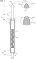
- Fig. 1 is a diagram illustrating a configuration example of the contact probe 1 according to the present embodiment, in which a barrel 10 is illustrated in a longitudinal cross section.
- the contact probe 1 includes the barrel 10, a first plunger 30, a second plunger 50, and a spring 70.
- the first plunger 30 projects from one end of the barrel 10 and the second plunger 50 projects from the other end of the barrel 10.
- the barrel 10 is a cylindrical body opened at both ends, and is made of a conductive material such as copper or a copper alloy. Alternatively, the barrel 10 may be obtained by covering, with a conductive material, surfaces (the inner side surface and the outer side surface) of a cylindrical body formed of a nonconductive material.
- the barrel 10 holds the first plunger 30 at the one end side of the barrel 10 as the upper side in Fig. 1 in a manner slidable in the axial direction, and holds the second plunger 50 at the other end side of the barrel 10 as lower end side in Fig. 1 in a manner slidable in the axial direction. Opening ends at both ends are bent inward to form locking portions 11 and 13, respectively, thereby preventing the first plunger 30 and the second plunger 50 from coming off the barrel 10.
- the first plunger 30 includes a projection 31 and a base end portion 33 having a larger diameter than that of the projection 31.
- a tip portion 311, which is the tip of the projection 31, is a contact portion that comes into contact with the semiconductor device as the inspection object.
- a shape of the tip portion 311 is illustrated as a conical shape.
- the first plunger 30 is configured to prevent the first plunger 30 from coming off from the barrel 10 to the upper side in Fig. 1 when a tapered stepped portion 35 between the projection 31 and the base end portion 33 comes into contact with the locking portion 11 of the barrel 10.
- the base end portion 33 of the first plunger 30 is arranged in the barrel 10 and slides on the inner circumferential surface of the barrel 10.
- the projection limit length which is the length by which the tip portion 311 can project most with respect to the barrel 10, can be defined by the length of the projection 31.
- the length of the projection 31 is designed in accordance with the projection limit length corresponding to the required specification.
- the first plunger 30 is made of a conductive material. Specifically, the first plunger 30 is configured such that the surface of the base end portion 33 is formed of gold (Au) and the surface of the tip portion 311 is formed of a metal material other than gold. A longitudinal cross-sectional view of the first plunger 30 in the vicinity of the stepped portion 35 is illustrated as a partially enlarged view surrounded by a one-dot chain line in Fig. 1 .
- the first plunger 30 has a layered configuration in which a surface layer 303 formed of gold is formed as an outermost layer outside a plunger base material 301 as a base material.
- a longitudinal cross-sectional view of the first plunger 30 in the vicinity of the tip portion 311 is illustrated as a partially enlarged view surrounded by a two-dot chain line in Fig. 1 .
- the surface layer 303 formed of gold is removed from the tip portion 311, and the plunger base material 301 is exposed at the tip portion 311.
- the first plunger 30 is configured such that the plunger base material 301 is exposed only at the tip portion 311, and the portions other than the tip portion 311 are covered with the surface layer 303 formed of gold.
- the plunger base material 301 is manufactured.
- an alloy of palladium, silver, copper (palladium alloy), or the like is used.
- a metal material such as beryllium copper can be used.
- a metal material corresponding to the semiconductor device as the inspection object can be selected.
- the surface layer 303 formed of gold is formed on the entire outer side of the plunger base material 301.
- the surface layer 303 can be formed by surface treatment such as electroplating or hot-dip plating.
- the surface layer 303 is removed from the tip portion of the projection 31 to expose the plunger base material 301 on the inner side (that is, the palladium alloy), thereby forming the tip portion 311 whose surface is formed of the palladium alloy.
- the removal of the surface layer 303 can be realized by processing such as removal by laser or etching, or cutting. More specifically, the portion in contact with the semiconductor device as the inspection object is a portion having a length L1 of 0.1 mm or less from the projection end of the projection 31.
- a portion within 0.1 mm from projection end of the projection 31 is set as the tip portion 311, and the surface layer 303 of the portion within 0.1 mm is removed, whereby a length of the tip portion 311 is set to a length within 0.1 mm from the projection end of the projection 31.
- the range in which the palladium alloy of the plunger base material 301 is exposed is not limited to the tip portion 311 within 0.1 mm from the projection end.
- the range may be within 0.5 mm or within 1 mm from the projection end of the projection 31.
- the surface layer 303 formed of gold is only required to be formed at least on the surface of the base end portion 33 that slides on the inner circumferential surface of the barrel 10. Therefore, the surface layer 303 may be removed over the entire region of the projection 31 to expose the palladium alloy.
- a coating layer formed of palladium alloy is formed on the portion within 0.1 mm from the projection end of the projection 31 to become the tip portion 311.
- the surface of the tip portion 311 is formed of the palladium alloy, and the surface of the other portions including the base end portion 33 is formed of gold.
- the coating layer formed of palladium alloy can be formed by surface treatment such as electroplating or hot-dip plating.
- the plunger base material 301 in this case is not limited to a configuration formed of a metal material such as a palladium alloy, and may be formed of a nonconductive material.
- the first plunger 30 can be manufactured without being limited to the method of forming the surface layer 303 formed of gold on the entire outside of the plunger base material 301 and then removing a part thereof, but also by forming the surface layer 303 formed of gold in a partial region on the outer side of the plunger base material 301.
- the surface of the base end portion 33 may be formed of gold.
- the forming method may be, for example, a method of forming the surface layer 303 formed of gold on the surface of a large-diameter portion to become the base end portion 33 in the plunger base material 301 by surface treatment such as electroplating or hot-dip plating.
- the second plunger 50 includes a projection 51 and a base end portion 53 having a larger diameter than that of the projection 51.
- the tip of the projection 51 is in contact with the inspection substrate.
- the second plunger 50 is configured to prevent the second plunger 50 from coming off from the barrel 10 to the lower side in Fig. 1 when a tapered stepped portion 55 between the projection 51 and the base end portion 53 comes into contact with the locking portion 13 of the barrel 10.
- the base end portion 53 of the second plunger 50 is arranged in the barrel 10 and slides on the inner circumferential surface of the barrel 10.
- the projection limit length which is the length by which the tip end of the projection 51 can project most with respect to the barrel 10, can be defined by the length of the projection 51. Accordingly, the length of the projection 51 is designed in accordance with the projection limit length corresponding to the required specification.
- the second plunger 50 is made of a conductive material.
- the second plunger 50 has the same layered configuration made of the same metal material as that of the first plunger 30.
- the second plunger 50 may be made of a metal material different from that of the first plunger 30, or may have a layered configuration different from that of the first plunger 30.
- the spring 70 is a coil spring made from a piano wire or a stainless steel wire.
- the spring 70 is arranged in the barrel 10 and biases the first plunger 30 and the second plunger 50 in directions away from each other along the axial direction of the barrel 10. Accordingly, a contact force for the first plunger 30 to come into contact with the semiconductor device as the inspection object and a contact force for the second plunger 50 to come into contact with the inspection substrate can be applied by a single spring 70.
- the contact probe 1 configured as described above is used, for example, by being attached to a socket made of resin.
- the socket has a plurality of through holes, and each through hole is inserted with the contact probe 1. Between both surfaces of the socket, the tip end side of the first plunger 30 of each contact probe 1 projects from one surface, and the tip end side of the second plunger 50 of each contact probe 1 projects from the other surface.
- the socket is positioned and placed on the inspection substrate such that the tip of the second plunger 50 (the tip of the projection 51) of each contact probe 1 is in contact with an electrode of the inspection substrate.
- the semiconductor device as the inspection object is moved toward the socket so that the electrode of the semiconductor device comes into contact with the tip of the first plunger 30 of each contact probe 1 (the tip portion 311 of the projection 31).
- the semiconductor device as the inspection object is a BGA package
- the BGA package is moved such that the tip portion 311 of the first plunger 30 comes into contact with the solder ball surface of the BGA package.
- the semiconductor device as the inspection object and the inspection substrate are electrically connected to each other via the first plunger 30, the barrel 10, the spring 70, and the second plunger 50 of the contact probe 1. Thereafter, electrical inspection is performed on the semiconductor device.
- the surface of the tip portion 311 of the movable first plunger 30 in contact with the semiconductor device can be formed of a metal material other than gold, and the surface of the base end portion 33 in contact with the barrel can be formed of gold.
- the surface of the tip portion 311 can be formed of a metal material corresponding to the semiconductor device.
- the metal material of the surface of the tip portion 311 may be a palladium alloy which has a high contact property with tin (Sn) had in the solder ball.
- the contact reliability between the tip portion 311 and the semiconductor device can be increased, and the low contact resistance between the base end portion 33 and the barrel 10 can be ensured.
- the surface of the tip portion 311 and the surface of the base end portion 33 are formed of the same metal material, it is possible to improve the conductivity inside the contact probe 1 while securing the conductivity between the semiconductor device as the inspection object and the contact probe 1.
- Embodiments to which the present invention can be applied are not limited to the above-described embodiments, and components may be appropriately added, omitted, or changed.
- the first plunger may have an inner layer formed of a palladium alloy or the like as the base of a surface layer formed of gold.
- Fig. 2 is a longitudinal cross-sectional view of the vicinity of a tip portion 311a of a first plunger 30a in the present modification.
- the first plunger 30a illustrated in Fig. 2 is configured such that the outer side of the plunger base material 301a is formed with an intermediate layer 302a formed of, for example, a palladium alloy as an intermediate layer, and the outer side of the intermediate layer 302a is formed with a surface layer 303a formed of gold as an outermost layer.
- the surface layer 303a is removed, and the palladium alloy of the intermediate layer 302a is exposed.
- the plunger base material 301a is made of, for example, a palladium alloy, beryllium copper, or the like as in the above-described embodiment.
- the intermediate layer 302a may be formed as a plated coating film mainly having palladium (Pd) and/or rhodium (Rh).
- the plunger base material 301a may be formed of a nonconductive material.
- any layered configuration may be adopted as long as the outer side of the plunger base material 301a is provided with the intermediate layer 302a formed of palladium alloy and the outer side of the intermediate layer 302a is formed with the surface layer 303a formed of gold as the outermost layer, as in the configuration illustrated in Fig. 2 .
- the shape of the tip portion 311 of the first plunger 30 is exemplified as a conical shape, but the shape of the tip portion is not particularly limited.
- other shapes such as a pyramid shape, a spherical shape, a flat shape, and a crown shape can be appropriately selected depending on the semiconductor device as the inspection object.
- Fig. 3 is a perspective view illustrating the vicinity of a tip portion 311b of a first plunger 30b whose tip has a crown shape.
- the manufacture can be performed by the same procedure as in the above-described embodiments. Specifically, the surface layer 303 formed of gold is formed on the entire outer side of the plunger base material 301b whose tip portion has the corresponding tip shape (crown shape in the example of Fig. 3 ), and then the plunger base material 301b is exposed by removing the surface layer 303b of the tip portion.
- the crown-shaped tip portion 311b has a length L11 from the projection end of about 0.05 mm to 0.1 mm.
- the surface layer 303b of the tip portion is removed, whereby the tip portion 311b is set to a length of 0.1 mm or less.
- the first plunger may have an integrated structure in which the portion in contact with the barrel (base end portion) is formed of gold and the tip portion in contact with the semiconductor device is formed of a metal material different from gold.
- the tip portion may be an embedded member that is embedded in the plunger base material.
- Fig. 4 is a perspective view illustrating a tip portion of a first plunger 30c in the present modification.
- the first plunger 30c of the present modification includes a plunger body 37c and an embedded member 39c that forms a tip portion, and has a structure in which the embedded member 39c is embedded in the tip of the plunger body 37c.
- the embedded member 39c is made of a metal material corresponding to the semiconductor device as the inspection object, such as a palladium alloy.
- the plunger body 37c may have a layered configuration in which a surface layer of gold is formed on the entire outer side of the plunger base material.
- the plunger body 37c may have a layered configuration in which the inner layer (coating layer) exemplified in the first modification is formed between the plunger base material and the surface layer.
- the length by which the embedded member 39c projects and is exposed from the tip end of the plunger body 37c can be, for example, a length of 0.1 mm or less as in the above-described embodiments.
- An aspect of the present disclosure is a contact probe including: a first plunger including a tip portion and a base end portion; and a spring configured to bias the first plunger.
- a surface of the tip portion and a surface of the base end portion are formed of different metal materials from each other.
- the surface of the tip portion for coming into contact with the semiconductor device can be formed of a metal material different from the surface of the base end portion.
- the surface of the tip portion can be formed of a metal material corresponding to the semiconductor device as the inspection object. Therefore, as compared with the case where the surface of the tip portion and the surface of the base end portion are formed of the same metal material, it is possible to improve the conductivity inside the contact probe while securing the conductivity between the semiconductor device and the contact probe.
- the tip portion may have a length within 0.1 mm from a projection end.
- the surface can be formed of a metal material different from that of the base end portion while being limited in a range of 0.1 mm from the projection end.
- a portion in contact with the semiconductor device as the inspection object is the portion within 0.1 mm from the projection end. Therefore, without forming the surface of the tip portion with a metal material different from that of the surface of the base end portion in an unnecessarily wide range, the cost of forming the surface of the tip portion can be reduced.
- the first plunger may have a base material or an inner layer formed of a palladium alloy.
- the base portion may have an outermost layer formed of gold.
- the palladium alloy of the base material or the inner layer may be exposed in the tip portion.
- the surface of the tip portion of the first plunger can be formed of a palladium alloy and the surface of the base end portion can be formed of gold, it is possible to improve the conductivity inside the contact probe while securing the conductivity between the semiconductor device and the contact probe.
- the contact probe may further include a second plunger configured to come into contact with an inspection substrate.
- the spring may bias the first plunger and the second plunger in directions away from each other.
Landscapes
- Physics & Mathematics (AREA)
- General Physics & Mathematics (AREA)
- Measuring Leads Or Probes (AREA)
Abstract
Description
- The present invention relates to a contact probe.
- In inspection of electrical characteristics of an electronic component (a semiconductor device) such as an integrated circuit or a large-scale integrated circuit using semiconductor elements, a contact probe is used to electrically connect the semiconductor device as the inspection object to an inspection substrate. The contact probe includes a plunger for connection to the semiconductor device, and performs an energization test by bringing a tip portion of the plunger into elastic contact with an electrode of the semiconductor device. As the structure of the contact probe, for example, there has been a structure in which a plunger is slidable in a cylindrical barrel (for example, see Patent Literature 1).
- Patent Literature 1:
JP2019-082378A - The metal material forming the plunger is selected according to the semiconductor device as the inspection object. For example, in the case of a BGA (ball grid array) package, a palladium alloy is generally used to ensure the contact performance with respect to tin (Sn).
However, when a palladium alloy is used for the plunger and the barrel, the contact resistance between the plunger and the barrel is high due to the contact resistance properties of the palladium alloy. Therefore, the conductivity between the plunger and the barrel may be unstable. - An example of an object of the present invention is to improve the conductivity inside a contact probe while ensuring the conductivity between a semiconductor device as the inspection object and the contact probe. Other objects of the present invention will become apparent according to the present description.
- An aspect of the present invention is a contact probe including: a first plunger including a tip portion and a base end portion; and a spring configured to bias the first plunger. A surface of the tip portion and a surface of the base end portion are formed of different metal materials from each other.
- According to the above-described aspect of the present invention, it is possible to improve the conductivity inside a contact probe while ensuring the conductivity between a semiconductor device as the inspection object and the contact probe.
-
-
Fig. 1 is a diagram illustrating a configuration example of a contact probe: -
Fig. 2 is a diagram illustrating a configuration example of a first plunger in a first modification; -
Fig. 3 is a diagram illustrating a configuration example of a first plunger in a second modification; and -
Fig. 4 is a diagram illustrating a configuration example of a first plunger in a third modification. - Hereinafter, preferred embodiments of the present invention will be described with reference to the drawings. The present invention is not limited to the following embodiments, and forms to which the present invention can be applied are not limited to the following embodiments. In the drawings, the same components are denoted by the same reference signs. As an example, a contact probe 1 of the present embodiment is used such that a semiconductor device as the inspection object is a BGA package and the
first plunger 30 comes into contact with a solder ball of the BGA package. The solder ball has tin (Sn). -
Fig. 1 is a diagram illustrating a configuration example of the contact probe 1 according to the present embodiment, in which abarrel 10 is illustrated in a longitudinal cross section. The contact probe 1 includes thebarrel 10, afirst plunger 30, asecond plunger 50, and aspring 70. In the contact probe 1, due to thespring 70 provided in thebarrel 10 and biasing thefirst plunger 30 andsecond plunger 50, the first plunger 30 projects from one end of thebarrel 10 and the second plunger 50 projects from the other end of thebarrel 10. - The
barrel 10 is a cylindrical body opened at both ends, and is made of a conductive material such as copper or a copper alloy. Alternatively, thebarrel 10 may be obtained by covering, with a conductive material, surfaces (the inner side surface and the outer side surface) of a cylindrical body formed of a nonconductive material. Thebarrel 10 holds thefirst plunger 30 at the one end side of thebarrel 10 as the upper side inFig. 1 in a manner slidable in the axial direction, and holds thesecond plunger 50 at the other end side of thebarrel 10 as lower end side inFig. 1 in a manner slidable in the axial direction. Opening ends at both ends are bent inward to form lockingportions first plunger 30 and thesecond plunger 50 from coming off thebarrel 10. - The
first plunger 30 includes aprojection 31 and abase end portion 33 having a larger diameter than that of theprojection 31. Atip portion 311, which is the tip of theprojection 31, is a contact portion that comes into contact with the semiconductor device as the inspection object. InFig. 1 , a shape of thetip portion 311 is illustrated as a conical shape. Thefirst plunger 30 is configured to prevent thefirst plunger 30 from coming off from thebarrel 10 to the upper side inFig. 1 when a tapered steppedportion 35 between theprojection 31 and thebase end portion 33 comes into contact with thelocking portion 11 of thebarrel 10. As a result, thebase end portion 33 of thefirst plunger 30 is arranged in thebarrel 10 and slides on the inner circumferential surface of thebarrel 10. The projection limit length, which is the length by which thetip portion 311 can project most with respect to thebarrel 10, can be defined by the length of theprojection 31. The length of theprojection 31 is designed in accordance with the projection limit length corresponding to the required specification. - The
first plunger 30 is made of a conductive material. Specifically, thefirst plunger 30 is configured such that the surface of thebase end portion 33 is formed of gold (Au) and the surface of thetip portion 311 is formed of a metal material other than gold. A longitudinal cross-sectional view of thefirst plunger 30 in the vicinity of thestepped portion 35 is illustrated as a partially enlarged view surrounded by a one-dot chain line inFig. 1 . Thefirst plunger 30 has a layered configuration in which asurface layer 303 formed of gold is formed as an outermost layer outside aplunger base material 301 as a base material. A longitudinal cross-sectional view of thefirst plunger 30 in the vicinity of thetip portion 311 is illustrated as a partially enlarged view surrounded by a two-dot chain line inFig. 1 . In thefirst plunger 30, thesurface layer 303 formed of gold is removed from thetip portion 311, and theplunger base material 301 is exposed at thetip portion 311. In this way, thefirst plunger 30 is configured such that theplunger base material 301 is exposed only at thetip portion 311, and the portions other than thetip portion 311 are covered with thesurface layer 303 formed of gold. - In the manufacturing procedure of the
first plunger 30, first, theplunger base material 301 is manufactured. In the present embodiment, an alloy of palladium, silver, copper (palladium alloy), or the like is used. Alternatively, for example, a metal material such as beryllium copper can be used. A metal material corresponding to the semiconductor device as the inspection object can be selected. - Next, the
surface layer 303 formed of gold is formed on the entire outer side of theplunger base material 301. Thesurface layer 303 can be formed by surface treatment such as electroplating or hot-dip plating. - Then, the
surface layer 303 is removed from the tip portion of theprojection 31 to expose theplunger base material 301 on the inner side (that is, the palladium alloy), thereby forming thetip portion 311 whose surface is formed of the palladium alloy. The removal of thesurface layer 303 can be realized by processing such as removal by laser or etching, or cutting. More specifically, the portion in contact with the semiconductor device as the inspection object is a portion having a length L1 of 0.1 mm or less from the projection end of theprojection 31. For this purpose, for example, a portion within 0.1 mm from projection end of theprojection 31 is set as thetip portion 311, and thesurface layer 303 of the portion within 0.1 mm is removed, whereby a length of thetip portion 311 is set to a length within 0.1 mm from the projection end of theprojection 31. According to this, without exposing the plunger base material 301 (palladium alloy) in an unnecessarily wide range, the cost of removing thesurface layer 303 can be reduced. - The range in which the palladium alloy of the
plunger base material 301 is exposed is not limited to thetip portion 311 within 0.1 mm from the projection end. For example, the range may be within 0.5 mm or within 1 mm from the projection end of theprojection 31. Thesurface layer 303 formed of gold is only required to be formed at least on the surface of thebase end portion 33 that slides on the inner circumferential surface of thebarrel 10. Therefore, thesurface layer 303 may be removed over the entire region of theprojection 31 to expose the palladium alloy. - Alternatively, after the
surface layer 303 formed of gold is formed on the entire outer side of theplunger base material 301, a coating layer formed of palladium alloy is formed on the portion within 0.1 mm from the projection end of theprojection 31 to become thetip portion 311. In this way, in thefirst plunger 30, the surface of thetip portion 311 is formed of the palladium alloy, and the surface of the other portions including thebase end portion 33 is formed of gold. This configuration may be adopted as well. The coating layer formed of palladium alloy can be formed by surface treatment such as electroplating or hot-dip plating. Theplunger base material 301 in this case is not limited to a configuration formed of a metal material such as a palladium alloy, and may be formed of a nonconductive material. - The
first plunger 30 can be manufactured without being limited to the method of forming thesurface layer 303 formed of gold on the entire outside of theplunger base material 301 and then removing a part thereof, but also by forming thesurface layer 303 formed of gold in a partial region on the outer side of theplunger base material 301. For example, the surface of thebase end portion 33 may be formed of gold. The forming method may be, for example, a method of forming thesurface layer 303 formed of gold on the surface of a large-diameter portion to become thebase end portion 33 in theplunger base material 301 by surface treatment such as electroplating or hot-dip plating. - Similarly to the
first plunger 30, thesecond plunger 50 includes aprojection 51 and abase end portion 53 having a larger diameter than that of theprojection 51. The tip of theprojection 51 is in contact with the inspection substrate. Thesecond plunger 50 is configured to prevent thesecond plunger 50 from coming off from thebarrel 10 to the lower side inFig. 1 when a tapered steppedportion 55 between theprojection 51 and thebase end portion 53 comes into contact with the lockingportion 13 of thebarrel 10. As a result, thebase end portion 53 of thesecond plunger 50 is arranged in thebarrel 10 and slides on the inner circumferential surface of thebarrel 10. The projection limit length, which is the length by which the tip end of theprojection 51 can project most with respect to thebarrel 10, can be defined by the length of theprojection 51. Accordingly, the length of theprojection 51 is designed in accordance with the projection limit length corresponding to the required specification. - The
second plunger 50 is made of a conductive material. For example, thesecond plunger 50 has the same layered configuration made of the same metal material as that of thefirst plunger 30. Alternatively, thesecond plunger 50 may be made of a metal material different from that of thefirst plunger 30, or may have a layered configuration different from that of thefirst plunger 30. - The
spring 70 is a coil spring made from a piano wire or a stainless steel wire. Thespring 70 is arranged in thebarrel 10 and biases thefirst plunger 30 and thesecond plunger 50 in directions away from each other along the axial direction of thebarrel 10. Accordingly, a contact force for thefirst plunger 30 to come into contact with the semiconductor device as the inspection object and a contact force for thesecond plunger 50 to come into contact with the inspection substrate can be applied by asingle spring 70. - The contact probe 1 configured as described above is used, for example, by being attached to a socket made of resin. The socket has a plurality of through holes, and each through hole is inserted with the contact probe 1. Between both surfaces of the socket, the tip end side of the
first plunger 30 of each contact probe 1 projects from one surface, and the tip end side of thesecond plunger 50 of each contact probe 1 projects from the other surface. The socket is positioned and placed on the inspection substrate such that the tip of the second plunger 50 (the tip of the projection 51) of each contact probe 1 is in contact with an electrode of the inspection substrate. Then, the semiconductor device as the inspection object is moved toward the socket so that the electrode of the semiconductor device comes into contact with the tip of thefirst plunger 30 of each contact probe 1 (thetip portion 311 of the projection 31). If the semiconductor device as the inspection object is a BGA package, the BGA package is moved such that thetip portion 311 of thefirst plunger 30 comes into contact with the solder ball surface of the BGA package. Thus, the semiconductor device as the inspection object and the inspection substrate are electrically connected to each other via thefirst plunger 30, thebarrel 10, thespring 70, and thesecond plunger 50 of the contact probe 1. Thereafter, electrical inspection is performed on the semiconductor device. - According to the present embodiment, in the contact probe 1 having the structure in which the
first plunger 30 on the side in contact with the semiconductor device is movable, the surface of thetip portion 311 of the movablefirst plunger 30 in contact with the semiconductor device can be formed of a metal material other than gold, and the surface of thebase end portion 33 in contact with the barrel can be formed of gold. Specifically, the surface of thetip portion 311 can be formed of a metal material corresponding to the semiconductor device. For example, when the inspection object is a BGA package, the metal material of the surface of thetip portion 311 may be a palladium alloy which has a high contact property with tin (Sn) had in the solder ball. According to this, the contact reliability between thetip portion 311 and the semiconductor device can be increased, and the low contact resistance between thebase end portion 33 and thebarrel 10 can be ensured. Thus, as compared with the case where the surface of thetip portion 311 and the surface of thebase end portion 33 are formed of the same metal material, it is possible to improve the conductivity inside the contact probe 1 while securing the conductivity between the semiconductor device as the inspection object and the contact probe 1. - Embodiments to which the present invention can be applied are not limited to the above-described embodiments, and components may be appropriately added, omitted, or changed.
- For example, the first plunger may have an inner layer formed of a palladium alloy or the like as the base of a surface layer formed of gold.
Fig. 2 is a longitudinal cross-sectional view of the vicinity of atip portion 311a of a first plunger 30a in the present modification. The first plunger 30a illustrated inFig. 2 is configured such that the outer side of theplunger base material 301a is formed with anintermediate layer 302a formed of, for example, a palladium alloy as an intermediate layer, and the outer side of theintermediate layer 302a is formed with asurface layer 303a formed of gold as an outermost layer. In thetip portion 311a, thesurface layer 303a is removed, and the palladium alloy of theintermediate layer 302a is exposed. Theplunger base material 301a is made of, for example, a palladium alloy, beryllium copper, or the like as in the above-described embodiment. Theintermediate layer 302a may be formed as a plated coating film mainly having palladium (Pd) and/or rhodium (Rh). - Alternatively, the
plunger base material 301a may be formed of a nonconductive material. In this case as well, any layered configuration may be adopted as long as the outer side of theplunger base material 301a is provided with theintermediate layer 302a formed of palladium alloy and the outer side of theintermediate layer 302a is formed with thesurface layer 303a formed of gold as the outermost layer, as in the configuration illustrated inFig. 2 . - In the above-described embodiment, the shape of the
tip portion 311 of thefirst plunger 30 is exemplified as a conical shape, but the shape of the tip portion is not particularly limited. For example, other shapes such as a pyramid shape, a spherical shape, a flat shape, and a crown shape can be appropriately selected depending on the semiconductor device as the inspection object. -
Fig. 3 is a perspective view illustrating the vicinity of atip portion 311b of afirst plunger 30b whose tip has a crown shape. When the tip shape is different, the manufacture can be performed by the same procedure as in the above-described embodiments. Specifically, thesurface layer 303 formed of gold is formed on the entire outer side of theplunger base material 301b whose tip portion has the corresponding tip shape (crown shape in the example ofFig. 3 ), and then theplunger base material 301b is exposed by removing thesurface layer 303b of the tip portion. The crown-shapedtip portion 311b has a length L11 from the projection end of about 0.05 mm to 0.1 mm. Therefore, for example, similarly to the above-described embodiment, with a portion having a length of 0.1 mm or less from the projection end being the tip portion, thesurface layer 303b of the tip portion is removed, whereby thetip portion 311b is set to a length of 0.1 mm or less. - The first plunger may have an integrated structure in which the portion in contact with the barrel (base end portion) is formed of gold and the tip portion in contact with the semiconductor device is formed of a metal material different from gold. For example, the tip portion may be an embedded member that is embedded in the plunger base material.
-
Fig. 4 is a perspective view illustrating a tip portion of afirst plunger 30c in the present modification. As illustrated inFig. 4 , thefirst plunger 30c of the present modification includes aplunger body 37c and an embeddedmember 39c that forms a tip portion, and has a structure in which the embeddedmember 39c is embedded in the tip of theplunger body 37c. The embeddedmember 39c is made of a metal material corresponding to the semiconductor device as the inspection object, such as a palladium alloy. On the other hand, theplunger body 37c may have a layered configuration in which a surface layer of gold is formed on the entire outer side of the plunger base material. Alternatively, theplunger body 37c may have a layered configuration in which the inner layer (coating layer) exemplified in the first modification is formed between the plunger base material and the surface layer. The length by which the embeddedmember 39c projects and is exposed from the tip end of theplunger body 37c can be, for example, a length of 0.1 mm or less as in the above-described embodiments. - Some embodiments and modifications thereof have been described. This disclosure can be summarized as follows.
- An aspect of the present disclosure is a contact probe including: a first plunger including a tip portion and a base end portion; and a spring configured to bias the first plunger. A surface of the tip portion and a surface of the base end portion are formed of different metal materials from each other.
- According to the aspect of the present disclosure, in the first plunger, the surface of the tip portion for coming into contact with the semiconductor device can be formed of a metal material different from the surface of the base end portion. For example, the surface of the tip portion can be formed of a metal material corresponding to the semiconductor device as the inspection object. Therefore, as compared with the case where the surface of the tip portion and the surface of the base end portion are formed of the same metal material, it is possible to improve the conductivity inside the contact probe while securing the conductivity between the semiconductor device and the contact probe.
- The tip portion may have a length within 0.1 mm from a projection end.
- Accordingly, the surface can be formed of a metal material different from that of the base end portion while being limited in a range of 0.1 mm from the projection end. At the tip portion, a portion in contact with the semiconductor device as the inspection object is the portion within 0.1 mm from the projection end. Therefore, without forming the surface of the tip portion with a metal material different from that of the surface of the base end portion in an unnecessarily wide range, the cost of forming the surface of the tip portion can be reduced.
- The first plunger may have a base material or an inner layer formed of a palladium alloy. The base portion may have an outermost layer formed of gold. The palladium alloy of the base material or the inner layer may be exposed in the tip portion.
- Since the surface of the tip portion of the first plunger can be formed of a palladium alloy and the surface of the base end portion can be formed of gold, it is possible to improve the conductivity inside the contact probe while securing the conductivity between the semiconductor device and the contact probe.
- The contact probe may further include a second plunger configured to come into contact with an inspection substrate. The spring may bias the first plunger and the second plunger in directions away from each other.
-
- 1: contact probe
- 10: barrel
- 30, 30a, 30b, 30c: first plunger
- 301, 301a, 301b : plunger base material
- 302a: intermediate layer
- 303, 303a, 303b : surface layer
- 311, 311a, 311b : tip portion
- 37c : plunger body
- 39c: embedded member
- 33: base portion
- 50: second plunger
- 70: spring
Claims (4)
- A contact probe comprising:a first plunger including a tip portion and a base end portion; anda spring configured to bias the first plunger, whereina surface of the tip portion and a surface of the base end portion are formed of different metal materials from each other.
- The contact probe according to claim 1, wherein
the tip portion has a length within 0.1 mm from a projection end. - The contact probe according to claim 1 or 2, whereinthe first plunger has a base material or an inner layer formed of a palladium alloy,the base end portion has an outermost layer formed of gold, andthe palladium alloy of the base material or the inner layer is exposed in the tip portion.
- The contact probe according to any one of claims 1 to 3, further comprising:a second plunger configured to come into contact with an inspection substrate, whereinthe spring biases the first plunger and the second plunger in directions away from each other.
Applications Claiming Priority (2)
| Application Number | Priority Date | Filing Date | Title |
|---|---|---|---|
| JP2020177213 | 2020-10-22 | ||
| PCT/JP2021/037288 WO2022085483A1 (en) | 2020-10-22 | 2021-10-08 | Contact probe |
Publications (1)
| Publication Number | Publication Date |
|---|---|
| EP4235191A1 true EP4235191A1 (en) | 2023-08-30 |
Family
ID=81290394
Family Applications (1)
| Application Number | Title | Priority Date | Filing Date |
|---|---|---|---|
| EP21882624.6A Withdrawn EP4235191A1 (en) | 2020-10-22 | 2021-10-08 | Contact probe |
Country Status (6)
| Country | Link |
|---|---|
| US (1) | US20230393171A1 (en) |
| EP (1) | EP4235191A1 (en) |
| JP (1) | JPWO2022085483A1 (en) |
| CN (1) | CN116324427A (en) |
| TW (1) | TW202225697A (en) |
| WO (1) | WO2022085483A1 (en) |
Families Citing this family (3)
| Publication number | Priority date | Publication date | Assignee | Title |
|---|---|---|---|---|
| TWI835228B (en) * | 2022-07-29 | 2024-03-11 | 晝思有限公司 | Probe heads and probe components |
| JP2024162092A (en) * | 2023-05-09 | 2024-11-21 | 株式会社日本マイクロニクス | Probes and Electrical Connection Devices |
| JP2025018225A (en) * | 2023-07-26 | 2025-02-06 | 株式会社日本マイクロニクス | probe |
Family Cites Families (21)
| Publication number | Priority date | Publication date | Assignee | Title |
|---|---|---|---|---|
| JP4889183B2 (en) * | 2000-06-16 | 2012-03-07 | 日本発條株式会社 | Micro contactor probe and electrical probe unit |
| US6603323B1 (en) * | 2000-07-10 | 2003-08-05 | Formfactor, Inc. | Closed-grid bus architecture for wafer interconnect structure |
| JP2007232704A (en) * | 2006-03-02 | 2007-09-13 | Jinko Nishio | Contact probe |
| WO2009102030A1 (en) * | 2008-02-14 | 2009-08-20 | Nhk Spring Co., Ltd. | Probe unit |
| US8154316B2 (en) * | 2008-12-11 | 2012-04-10 | Fluke Corporation | Method and apparatus for indexing an adjustable test probe tip |
| DE102009016181A1 (en) * | 2009-04-03 | 2010-10-14 | Atg Luther & Maelzer Gmbh | Contacting unit for a test device for testing printed circuit boards |
| JP2011180034A (en) * | 2010-03-02 | 2011-09-15 | Citizen Tohoku Kk | Plunger for contact probe |
| JP2011226786A (en) * | 2010-04-15 | 2011-11-10 | Tokyo Electron Ltd | Contact structure and method of manufacturing the same |
| JP2012122905A (en) * | 2010-12-09 | 2012-06-28 | Rika Denshi Co Ltd | Contact probe |
| JPWO2013018809A1 (en) * | 2011-08-02 | 2015-03-05 | 日本発條株式会社 | Probe unit |
| WO2013051674A1 (en) * | 2011-10-07 | 2013-04-11 | 日本発條株式会社 | Probe unit |
| JP2013088389A (en) * | 2011-10-21 | 2013-05-13 | Tokyo Electron Ltd | Contact terminal for probe card and the probe card |
| US8860446B2 (en) * | 2012-05-24 | 2014-10-14 | Texas Instruments Incorporated | Multiple contact test probe |
| SG11201500755SA (en) * | 2012-08-03 | 2015-05-28 | Yamamoto Precious Metal Co Ltd | Alloy material, contact probe, and connection terminal |
| US10132833B2 (en) * | 2013-07-09 | 2018-11-20 | Formfactor, Inc. | Multipath electrical probe and probe assemblies with signal paths through secondary paths between electrically conductive guide plates |
| US20160025776A1 (en) * | 2014-07-24 | 2016-01-28 | Qualcomm Incorporated | Probes and probe assemblies for wafer probing |
| US10168357B2 (en) * | 2015-12-21 | 2019-01-01 | Intel Corporation | Coated probe tips for plunger pins of an integrated circuit package test system |
| JP6837283B2 (en) * | 2016-02-29 | 2021-03-03 | 株式会社ヨコオ | socket |
| JP6832661B2 (en) * | 2016-09-28 | 2021-02-24 | 株式会社日本マイクロニクス | Probe card and contact inspection device |
| JP6837665B2 (en) | 2017-10-30 | 2021-03-03 | 株式会社サンケイエンジニアリング | Contact probe |
| WO2020158575A1 (en) * | 2019-01-29 | 2020-08-06 | 株式会社ヨコオ | Plunger and contact probe |
-
2021
- 2021-10-08 JP JP2022556901A patent/JPWO2022085483A1/ja active Pending
- 2021-10-08 WO PCT/JP2021/037288 patent/WO2022085483A1/en not_active Ceased
- 2021-10-08 CN CN202180070948.2A patent/CN116324427A/en active Pending
- 2021-10-08 EP EP21882624.6A patent/EP4235191A1/en not_active Withdrawn
- 2021-10-08 US US18/033,084 patent/US20230393171A1/en not_active Abandoned
- 2021-10-22 TW TW110139311A patent/TW202225697A/en unknown
Also Published As
| Publication number | Publication date |
|---|---|
| WO2022085483A1 (en) | 2022-04-28 |
| TW202225697A (en) | 2022-07-01 |
| CN116324427A (en) | 2023-06-23 |
| US20230393171A1 (en) | 2023-12-07 |
| JPWO2022085483A1 (en) | 2022-04-28 |
Similar Documents
| Publication | Publication Date | Title |
|---|---|---|
| US6072324A (en) | Method for testing semiconductor packages using oxide penetrating test contacts | |
| US20230393171A1 (en) | Contact probe | |
| JP4060919B2 (en) | Electrical connection device, contact manufacturing method, and semiconductor test method | |
| US6781390B2 (en) | Conductive coil contact member | |
| US20090212807A1 (en) | Probe of cantilever probe card | |
| JP2014025737A (en) | Inspecting tool and contact | |
| US11360118B2 (en) | Contact probe and inspecting socket including the same | |
| KR20190001939A (en) | Contact probe and inspection jig | |
| JP3342789B2 (en) | Conductive contact | |
| KR20080027182A (en) | Connection | |
| US9642255B2 (en) | Membrane sheet with bumps for probe card, probe card and method for manufacturing membrane sheet with bumps for probe card | |
| JP2011180034A (en) | Plunger for contact probe | |
| JP2010139344A (en) | Contact pin and contact probe | |
| JP2021043100A (en) | Contact probe and inspection socket equipped with it | |
| CN114088997A (en) | Electrical contact structure of electrical contact and electrical connection device | |
| JPH0666834A (en) | Probe device | |
| KR100811740B1 (en) | Probe Needle Tube and Manufacturing Method Thereof | |
| US11977100B2 (en) | Inspection jig | |
| KR101416477B1 (en) | Probe card | |
| CN120112798A (en) | Spring needle probe and spring needle provided with same | |
| US20230349946A1 (en) | Tubular body, contact terminal, inspection jig, and inspection apparatus | |
| KR200328984Y1 (en) | Test socket for high frequency | |
| KR102763456B1 (en) | Method of manufacturing probe tip and probe tip manufactured by the same | |
| US20220178987A1 (en) | Inspection jig, and inspection device | |
| US20190334271A1 (en) | Contact and substrate |
Legal Events
| Date | Code | Title | Description |
|---|---|---|---|
| STAA | Information on the status of an ep patent application or granted ep patent |
Free format text: STATUS: THE INTERNATIONAL PUBLICATION HAS BEEN MADE |
|
| PUAI | Public reference made under article 153(3) epc to a published international application that has entered the european phase |
Free format text: ORIGINAL CODE: 0009012 |
|
| STAA | Information on the status of an ep patent application or granted ep patent |
Free format text: STATUS: REQUEST FOR EXAMINATION WAS MADE |
|
| 17P | Request for examination filed |
Effective date: 20230328 |
|
| AK | Designated contracting states |
Kind code of ref document: A1 Designated state(s): AL AT BE BG CH CY CZ DE DK EE ES FI FR GB GR HR HU IE IS IT LI LT LU LV MC MK MT NL NO PL PT RO RS SE SI SK SM TR |
|
| DAV | Request for validation of the european patent (deleted) | ||
| DAX | Request for extension of the european patent (deleted) | ||
| STAA | Information on the status of an ep patent application or granted ep patent |
Free format text: STATUS: THE APPLICATION HAS BEEN WITHDRAWN |
|
| 18W | Application withdrawn |
Effective date: 20240516 |