EP4234518A1 - Joined body, ceramic-copper circuit board, and semiconductor device - Google Patents
Joined body, ceramic-copper circuit board, and semiconductor device Download PDFInfo
- Publication number
- EP4234518A1 EP4234518A1 EP21882852.3A EP21882852A EP4234518A1 EP 4234518 A1 EP4234518 A1 EP 4234518A1 EP 21882852 A EP21882852 A EP 21882852A EP 4234518 A1 EP4234518 A1 EP 4234518A1
- Authority
- EP
- European Patent Office
- Prior art keywords
- region
- copper plate
- concentration
- copper
- less
- Prior art date
- Legal status (The legal status is an assumption and is not a legal conclusion. Google has not performed a legal analysis and makes no representation as to the accuracy of the status listed.)
- Pending
Links
Images

Classifications
-
- H—ELECTRICITY
- H10—SEMICONDUCTOR DEVICES; ELECTRIC SOLID-STATE DEVICES NOT OTHERWISE PROVIDED FOR
- H10W—GENERIC PACKAGES, INTERCONNECTIONS, CONNECTORS OR OTHER CONSTRUCTIONAL DETAILS OF DEVICES COVERED BY CLASS H10
- H10W40/00—Arrangements for thermal protection or thermal control
- H10W40/20—Arrangements for cooling
- H10W40/25—Arrangements for cooling characterised by their materials
- H10W40/255—Arrangements for cooling characterised by their materials having a laminate or multilayered structure, e.g. direct bond copper [DBC] ceramic substrates
-
- C—CHEMISTRY; METALLURGY
- C04—CEMENTS; CONCRETE; ARTIFICIAL STONE; CERAMICS; REFRACTORIES
- C04B—LIME, MAGNESIA; SLAG; CEMENTS; COMPOSITIONS THEREOF, e.g. MORTARS, CONCRETE OR LIKE BUILDING MATERIALS; ARTIFICIAL STONE; CERAMICS; REFRACTORIES; TREATMENT OF NATURAL STONE
- C04B37/00—Joining burned ceramic articles with other burned ceramic articles or other articles by heating
- C04B37/02—Joining burned ceramic articles with other burned ceramic articles or other articles by heating with metallic articles
-
- C—CHEMISTRY; METALLURGY
- C04—CEMENTS; CONCRETE; ARTIFICIAL STONE; CERAMICS; REFRACTORIES
- C04B—LIME, MAGNESIA; SLAG; CEMENTS; COMPOSITIONS THEREOF, e.g. MORTARS, CONCRETE OR LIKE BUILDING MATERIALS; ARTIFICIAL STONE; CERAMICS; REFRACTORIES; TREATMENT OF NATURAL STONE
- C04B37/00—Joining burned ceramic articles with other burned ceramic articles or other articles by heating
- C04B37/02—Joining burned ceramic articles with other burned ceramic articles or other articles by heating with metallic articles
- C04B37/023—Joining burned ceramic articles with other burned ceramic articles or other articles by heating with metallic articles characterised by the interlayer used
- C04B37/026—Joining burned ceramic articles with other burned ceramic articles or other articles by heating with metallic articles characterised by the interlayer used consisting of metals or metal salts
-
- H—ELECTRICITY
- H05—ELECTRIC TECHNIQUES NOT OTHERWISE PROVIDED FOR
- H05K—PRINTED CIRCUITS; CASINGS OR CONSTRUCTIONAL DETAILS OF ELECTRIC APPARATUS; MANUFACTURE OF ASSEMBLAGES OF ELECTRICAL COMPONENTS
- H05K1/00—Printed circuits
- H05K1/02—Details
- H05K1/09—Use of materials for the conductive, e.g. metallic pattern
-
- H—ELECTRICITY
- H10—SEMICONDUCTOR DEVICES; ELECTRIC SOLID-STATE DEVICES NOT OTHERWISE PROVIDED FOR
- H10W—GENERIC PACKAGES, INTERCONNECTIONS, CONNECTORS OR OTHER CONSTRUCTIONAL DETAILS OF DEVICES COVERED BY CLASS H10
- H10W70/00—Package substrates; Interposers; Redistribution layers [RDL]
- H10W70/60—Insulating or insulated package substrates; Interposers; Redistribution layers
- H10W70/67—Insulating or insulated package substrates; Interposers; Redistribution layers characterised by their insulating layers or insulating parts
- H10W70/69—Insulating materials thereof
- H10W70/692—Ceramics or glasses
-
- C—CHEMISTRY; METALLURGY
- C04—CEMENTS; CONCRETE; ARTIFICIAL STONE; CERAMICS; REFRACTORIES
- C04B—LIME, MAGNESIA; SLAG; CEMENTS; COMPOSITIONS THEREOF, e.g. MORTARS, CONCRETE OR LIKE BUILDING MATERIALS; ARTIFICIAL STONE; CERAMICS; REFRACTORIES; TREATMENT OF NATURAL STONE
- C04B2235/00—Aspects relating to ceramic starting mixtures or sintered ceramic products
- C04B2235/02—Composition of constituents of the starting material or of secondary phases of the final product
- C04B2235/50—Constituents or additives of the starting mixture chosen for their shape or used because of their shape or their physical appearance
- C04B2235/54—Particle size related information
- C04B2235/5418—Particle size related information expressed by the size of the particles or aggregates thereof
- C04B2235/5436—Particle size related information expressed by the size of the particles or aggregates thereof micrometer sized, i.e. from 1 to 100 micron
-
- C—CHEMISTRY; METALLURGY
- C04—CEMENTS; CONCRETE; ARTIFICIAL STONE; CERAMICS; REFRACTORIES
- C04B—LIME, MAGNESIA; SLAG; CEMENTS; COMPOSITIONS THEREOF, e.g. MORTARS, CONCRETE OR LIKE BUILDING MATERIALS; ARTIFICIAL STONE; CERAMICS; REFRACTORIES; TREATMENT OF NATURAL STONE
- C04B2235/00—Aspects relating to ceramic starting mixtures or sintered ceramic products
- C04B2235/65—Aspects relating to heat treatments of ceramic bodies such as green ceramics or pre-sintered ceramics, e.g. burning, sintering or melting processes
- C04B2235/656—Aspects relating to heat treatments of ceramic bodies such as green ceramics or pre-sintered ceramics, e.g. burning, sintering or melting processes characterised by specific heating conditions during heat treatment
- C04B2235/6565—Cooling rate
-
- C—CHEMISTRY; METALLURGY
- C04—CEMENTS; CONCRETE; ARTIFICIAL STONE; CERAMICS; REFRACTORIES
- C04B—LIME, MAGNESIA; SLAG; CEMENTS; COMPOSITIONS THEREOF, e.g. MORTARS, CONCRETE OR LIKE BUILDING MATERIALS; ARTIFICIAL STONE; CERAMICS; REFRACTORIES; TREATMENT OF NATURAL STONE
- C04B2235/00—Aspects relating to ceramic starting mixtures or sintered ceramic products
- C04B2235/65—Aspects relating to heat treatments of ceramic bodies such as green ceramics or pre-sintered ceramics, e.g. burning, sintering or melting processes
- C04B2235/658—Atmosphere during thermal treatment
- C04B2235/6581—Total pressure below 1 atmosphere, e.g. vacuum
-
- C—CHEMISTRY; METALLURGY
- C04—CEMENTS; CONCRETE; ARTIFICIAL STONE; CERAMICS; REFRACTORIES
- C04B—LIME, MAGNESIA; SLAG; CEMENTS; COMPOSITIONS THEREOF, e.g. MORTARS, CONCRETE OR LIKE BUILDING MATERIALS; ARTIFICIAL STONE; CERAMICS; REFRACTORIES; TREATMENT OF NATURAL STONE
- C04B2235/00—Aspects relating to ceramic starting mixtures or sintered ceramic products
- C04B2235/70—Aspects relating to sintered or melt-casted ceramic products
- C04B2235/74—Physical characteristics
- C04B2235/75—Products with a concentration gradient
-
- C—CHEMISTRY; METALLURGY
- C04—CEMENTS; CONCRETE; ARTIFICIAL STONE; CERAMICS; REFRACTORIES
- C04B—LIME, MAGNESIA; SLAG; CEMENTS; COMPOSITIONS THEREOF, e.g. MORTARS, CONCRETE OR LIKE BUILDING MATERIALS; ARTIFICIAL STONE; CERAMICS; REFRACTORIES; TREATMENT OF NATURAL STONE
- C04B2235/00—Aspects relating to ceramic starting mixtures or sintered ceramic products
- C04B2235/70—Aspects relating to sintered or melt-casted ceramic products
- C04B2235/74—Physical characteristics
- C04B2235/78—Grain sizes and shapes, product microstructures, e.g. acicular grains, equiaxed grains, platelet-structures
- C04B2235/786—Micrometer sized grains, i.e. from 1 to 100 micron
-
- C—CHEMISTRY; METALLURGY
- C04—CEMENTS; CONCRETE; ARTIFICIAL STONE; CERAMICS; REFRACTORIES
- C04B—LIME, MAGNESIA; SLAG; CEMENTS; COMPOSITIONS THEREOF, e.g. MORTARS, CONCRETE OR LIKE BUILDING MATERIALS; ARTIFICIAL STONE; CERAMICS; REFRACTORIES; TREATMENT OF NATURAL STONE
- C04B2235/00—Aspects relating to ceramic starting mixtures or sintered ceramic products
- C04B2235/70—Aspects relating to sintered or melt-casted ceramic products
- C04B2235/96—Properties of ceramic products, e.g. mechanical properties such as strength, toughness, wear resistance
-
- C—CHEMISTRY; METALLURGY
- C04—CEMENTS; CONCRETE; ARTIFICIAL STONE; CERAMICS; REFRACTORIES
- C04B—LIME, MAGNESIA; SLAG; CEMENTS; COMPOSITIONS THEREOF, e.g. MORTARS, CONCRETE OR LIKE BUILDING MATERIALS; ARTIFICIAL STONE; CERAMICS; REFRACTORIES; TREATMENT OF NATURAL STONE
- C04B2237/00—Aspects relating to ceramic laminates or to joining of ceramic articles with other articles by heating
- C04B2237/02—Aspects relating to interlayers, e.g. used to join ceramic articles with other articles by heating
- C04B2237/12—Metallic interlayers
- C04B2237/125—Metallic interlayers based on noble metals, e.g. silver
-
- C—CHEMISTRY; METALLURGY
- C04—CEMENTS; CONCRETE; ARTIFICIAL STONE; CERAMICS; REFRACTORIES
- C04B—LIME, MAGNESIA; SLAG; CEMENTS; COMPOSITIONS THEREOF, e.g. MORTARS, CONCRETE OR LIKE BUILDING MATERIALS; ARTIFICIAL STONE; CERAMICS; REFRACTORIES; TREATMENT OF NATURAL STONE
- C04B2237/00—Aspects relating to ceramic laminates or to joining of ceramic articles with other articles by heating
- C04B2237/02—Aspects relating to interlayers, e.g. used to join ceramic articles with other articles by heating
- C04B2237/12—Metallic interlayers
- C04B2237/126—Metallic interlayers wherein the active component for bonding is not the largest fraction of the interlayer
- C04B2237/127—The active component for bonding being a refractory metal
-
- C—CHEMISTRY; METALLURGY
- C04—CEMENTS; CONCRETE; ARTIFICIAL STONE; CERAMICS; REFRACTORIES
- C04B—LIME, MAGNESIA; SLAG; CEMENTS; COMPOSITIONS THEREOF, e.g. MORTARS, CONCRETE OR LIKE BUILDING MATERIALS; ARTIFICIAL STONE; CERAMICS; REFRACTORIES; TREATMENT OF NATURAL STONE
- C04B2237/00—Aspects relating to ceramic laminates or to joining of ceramic articles with other articles by heating
- C04B2237/30—Composition of layers of ceramic laminates or of ceramic or metallic articles to be joined by heating, e.g. Si substrates
- C04B2237/32—Ceramic
- C04B2237/34—Oxidic
- C04B2237/343—Alumina or aluminates
-
- C—CHEMISTRY; METALLURGY
- C04—CEMENTS; CONCRETE; ARTIFICIAL STONE; CERAMICS; REFRACTORIES
- C04B—LIME, MAGNESIA; SLAG; CEMENTS; COMPOSITIONS THEREOF, e.g. MORTARS, CONCRETE OR LIKE BUILDING MATERIALS; ARTIFICIAL STONE; CERAMICS; REFRACTORIES; TREATMENT OF NATURAL STONE
- C04B2237/00—Aspects relating to ceramic laminates or to joining of ceramic articles with other articles by heating
- C04B2237/30—Composition of layers of ceramic laminates or of ceramic or metallic articles to be joined by heating, e.g. Si substrates
- C04B2237/32—Ceramic
- C04B2237/34—Oxidic
- C04B2237/345—Refractory metal oxides
- C04B2237/348—Zirconia, hafnia, zirconates or hafnates
-
- C—CHEMISTRY; METALLURGY
- C04—CEMENTS; CONCRETE; ARTIFICIAL STONE; CERAMICS; REFRACTORIES
- C04B—LIME, MAGNESIA; SLAG; CEMENTS; COMPOSITIONS THEREOF, e.g. MORTARS, CONCRETE OR LIKE BUILDING MATERIALS; ARTIFICIAL STONE; CERAMICS; REFRACTORIES; TREATMENT OF NATURAL STONE
- C04B2237/00—Aspects relating to ceramic laminates or to joining of ceramic articles with other articles by heating
- C04B2237/30—Composition of layers of ceramic laminates or of ceramic or metallic articles to be joined by heating, e.g. Si substrates
- C04B2237/32—Ceramic
- C04B2237/36—Non-oxidic
- C04B2237/366—Aluminium nitride
-
- C—CHEMISTRY; METALLURGY
- C04—CEMENTS; CONCRETE; ARTIFICIAL STONE; CERAMICS; REFRACTORIES
- C04B—LIME, MAGNESIA; SLAG; CEMENTS; COMPOSITIONS THEREOF, e.g. MORTARS, CONCRETE OR LIKE BUILDING MATERIALS; ARTIFICIAL STONE; CERAMICS; REFRACTORIES; TREATMENT OF NATURAL STONE
- C04B2237/00—Aspects relating to ceramic laminates or to joining of ceramic articles with other articles by heating
- C04B2237/30—Composition of layers of ceramic laminates or of ceramic or metallic articles to be joined by heating, e.g. Si substrates
- C04B2237/32—Ceramic
- C04B2237/36—Non-oxidic
- C04B2237/368—Silicon nitride
-
- C—CHEMISTRY; METALLURGY
- C04—CEMENTS; CONCRETE; ARTIFICIAL STONE; CERAMICS; REFRACTORIES
- C04B—LIME, MAGNESIA; SLAG; CEMENTS; COMPOSITIONS THEREOF, e.g. MORTARS, CONCRETE OR LIKE BUILDING MATERIALS; ARTIFICIAL STONE; CERAMICS; REFRACTORIES; TREATMENT OF NATURAL STONE
- C04B2237/00—Aspects relating to ceramic laminates or to joining of ceramic articles with other articles by heating
- C04B2237/30—Composition of layers of ceramic laminates or of ceramic or metallic articles to be joined by heating, e.g. Si substrates
- C04B2237/40—Metallic
- C04B2237/407—Copper
-
- C—CHEMISTRY; METALLURGY
- C04—CEMENTS; CONCRETE; ARTIFICIAL STONE; CERAMICS; REFRACTORIES
- C04B—LIME, MAGNESIA; SLAG; CEMENTS; COMPOSITIONS THEREOF, e.g. MORTARS, CONCRETE OR LIKE BUILDING MATERIALS; ARTIFICIAL STONE; CERAMICS; REFRACTORIES; TREATMENT OF NATURAL STONE
- C04B2237/00—Aspects relating to ceramic laminates or to joining of ceramic articles with other articles by heating
- C04B2237/50—Processing aspects relating to ceramic laminates or to the joining of ceramic articles with other articles by heating
- C04B2237/58—Forming a gradient in composition or in properties across the laminate or the joined articles
-
- C—CHEMISTRY; METALLURGY
- C04—CEMENTS; CONCRETE; ARTIFICIAL STONE; CERAMICS; REFRACTORIES
- C04B—LIME, MAGNESIA; SLAG; CEMENTS; COMPOSITIONS THEREOF, e.g. MORTARS, CONCRETE OR LIKE BUILDING MATERIALS; ARTIFICIAL STONE; CERAMICS; REFRACTORIES; TREATMENT OF NATURAL STONE
- C04B2237/00—Aspects relating to ceramic laminates or to joining of ceramic articles with other articles by heating
- C04B2237/50—Processing aspects relating to ceramic laminates or to the joining of ceramic articles with other articles by heating
- C04B2237/70—Forming laminates or joined articles comprising layers of a specific, unusual thickness
- C04B2237/706—Forming laminates or joined articles comprising layers of a specific, unusual thickness of one or more of the metallic layers or articles
-
- C—CHEMISTRY; METALLURGY
- C04—CEMENTS; CONCRETE; ARTIFICIAL STONE; CERAMICS; REFRACTORIES
- C04B—LIME, MAGNESIA; SLAG; CEMENTS; COMPOSITIONS THEREOF, e.g. MORTARS, CONCRETE OR LIKE BUILDING MATERIALS; ARTIFICIAL STONE; CERAMICS; REFRACTORIES; TREATMENT OF NATURAL STONE
- C04B2237/00—Aspects relating to ceramic laminates or to joining of ceramic articles with other articles by heating
- C04B2237/50—Processing aspects relating to ceramic laminates or to the joining of ceramic articles with other articles by heating
- C04B2237/70—Forming laminates or joined articles comprising layers of a specific, unusual thickness
- C04B2237/708—Forming laminates or joined articles comprising layers of a specific, unusual thickness of one or more of the interlayers
-
- H—ELECTRICITY
- H05—ELECTRIC TECHNIQUES NOT OTHERWISE PROVIDED FOR
- H05K—PRINTED CIRCUITS; CASINGS OR CONSTRUCTIONAL DETAILS OF ELECTRIC APPARATUS; MANUFACTURE OF ASSEMBLAGES OF ELECTRICAL COMPONENTS
- H05K1/00—Printed circuits
- H05K1/02—Details
- H05K1/03—Use of materials for the substrate
- H05K1/0306—Inorganic insulating substrates, e.g. ceramic, glass
-
- H—ELECTRICITY
- H05—ELECTRIC TECHNIQUES NOT OTHERWISE PROVIDED FOR
- H05K—PRINTED CIRCUITS; CASINGS OR CONSTRUCTIONAL DETAILS OF ELECTRIC APPARATUS; MANUFACTURE OF ASSEMBLAGES OF ELECTRICAL COMPONENTS
- H05K3/00—Apparatus or processes for manufacturing printed circuits
- H05K3/38—Improvement of the adhesion between the insulating substrate and the metal
- H05K3/388—Improvement of the adhesion between the insulating substrate and the metal by the use of a metallic or inorganic thin film adhesion layer
Definitions
- Embodiments described below relate generally to a bonded body, a ceramic-copper circuit board, and a semiconductor device.
- Patent Document 1 discusses a ceramic-copper circuit board in which a ceramic substrate and a copper plate are bonded.
- the crystal grain size of the copper plate and the diffusion amount of Ag inside the copper plate are controlled.
- TCT temperature cycle test
- Patent Document 1 WO 2018/180965
- the diffusion amount of Ag into the copper plate is a cause.
- the diffusion amount of Ag is controlled by uniformly trisecting the copper plate in the thickness direction. The Ag diffusion amount is reduced from the vicinity of the bonding layer toward the copper plate front surface. The Ag inside the copper plate diffuses from the bonding layer. Therefore, the Ag amount was high at locations proximate to the bonding layer; and the Ag amount decreased toward the copper plate front surface. A thermal expansion difference occurs between high and low diffusion amounts of Ag in the copper plate. It was found that this partial difference of the diffusion amount of Ag is the cause of the inhibition of the improvement of the TCT characteristics.
- An object of the invention is to address such problems and to provide a bonded body in which the Ag concentration in the copper plate is controlled.
- a bonded body includes a ceramic substrate, a copper plate, and a bonding layer.
- the bonding layer is located on at least one surface of the ceramic substrate and bonds the ceramic substrate and the copper plate.
- the bonding layer includes Ag and Ti.
- the copper plate includes a first region, a second region, and a third region. The first region is separated from the bonding layer in a thickness direction.
- the second region is located between the bonding layer and the first region and has a higher Ag concentration than the first region.
- the third region is located between the bonding layer and the second region and has a lower Ag concentration than the second region.
- a bonded body includes a ceramic substrate, a copper plate, and a bonding layer.
- the bonding layer is located on at least one surface of the ceramic substrate and bonds the ceramic substrate and the copper plate.
- the bonding layer includes Ag and Ti.
- the copper plate includes a first region, a second region, and a third region. The first region is separated from the bonding layer in a thickness direction.
- the second region is located between the bonding layer and the first region and has a higher Ag concentration than the first region.
- the third region is located between the bonding layer and the second region and has a lower Ag concentration than the second region.
- FIG. 1 is a schematic view showing an example of a bonded body according to an embodiment.
- 1 is a bonded body
- 2 is a ceramic substrate
- 3 is a copper plate
- 4 is a bonding layer.
- FIG. 1 shows the bonded body 1 in which the copper plate 3 is located at each of two surfaces of the ceramic substrate 2 with the bonding layers 4 interposed.
- the longitudinal and lateral sizes of the ceramic substrate 2 are equal to the longitudinal and lateral sizes of the copper plate 3.
- the bonded body according to the embodiment is not limited to such a configuration.
- the bonded body 1 may have a structure in which the copper plate is located at only one surface of the bonded body 1.
- the longitudinal and lateral sizes of the ceramic substrate 2 may be different from the longitudinal and lateral sizes of the copper plate 3.
- FIG. 2 is a schematic view showing an example of a measurement region measuring the Ag concentration in a copper plate.
- 3 is a copper plate
- 4 is a bonding layer
- 5 is a measurement region
- T is the thickness of the copper plate
- P is the spacing (pitch) between the measurement regions.
- 5-1 is a first measurement region
- 5-2 is a second measurement region
- 5-3 is a third measurement region
- 5-4 is a fourth measurement region
- 5-5 is a fifth measurement region
- 5-6 is a sixth measurement region
- 5-7 is a seventh measurement region
- 5-n is an nth measurement region
- n examples of the measurement region are shown in FIG. 2 .
- any cross section of the bonded body 1 is set as the location to be measured.
- the cross section is a surface perpendicular to the direction connecting the ceramic substrate 2 and the copper plate 3. That is, the cross section is a surface perpendicular to the bonding surface of the ceramic substrate 2 and the copper plate 3.
- the pitch P of the multiple measurement regions is determined.
- the multiple measurement regions are arranged at uniform spacing at a pitch of not less than 30 ⁇ m and not more than 100 ⁇ m in the thickness direction of the copper plate 3.
- the pitch is the spacing P between the centers of the measurement regions arranged vertically.
- the spacing P between the centers of the measurement regions also is called the pitch P.
- the pitch P is a constant spacing within the range of 30 to 100 ⁇ m. For example, when the pitch P is set to be 50 ⁇ m, the pitch P is always 50 ⁇ m. Also, when the pitch P is set to be 100 ⁇ m, the pitch P is always 100 ⁇ m.
- the length in the width direction of one measurement region 5 is within the range of not less than 100 ⁇ m and not more than 200 ⁇ m.
- the length in the thickness direction of one measurement region 5 is within the range of not less than 10 ⁇ m and not more than 100 ⁇ m.
- the measurement region 5 is a quadrilateral defined by the width directionxthickness direction.
- the width direction is a direction parallel to the ceramic substrate 2 surface. That is, the width direction is a direction parallel to the copper plate 3 surface.
- the thickness direction is a direction perpendicular to the ceramic substrate 2 surface, and is the thickness direction of the copper plate 3.
- the measurement regions 5 are arranged in the thickness direction of the copper plate 3.
- One size is selected as the size of each measurement region 5 from the range of not less than 100 ⁇ m and not more than 200 ⁇ m in the width directionxnot less than 10 ⁇ m and not more than 100 ⁇ m in the thickness direction.
- the sizes of all of the measurement regions 5 are 150 ⁇ m in the width directionx50 ⁇ m in the thickness direction.
- the measurement regions are designated to match the pitch P described above.
- the pitch P is counted from the bonding surface of the copper plate 3. Positioning is performed to be alternately pitch P -> measurement region 5 -> pitch P -> measurement region 5.
- the measurement region that is most proximate to the bonding layer 4 is set as the first measurement region 5-1.
- the measurement region that is most distant to the bonding layer 4 is set as the nth measurement region 5-n.
- the Ag concentrations of the measurement regions 5 are measured using energy dispersive X-ray spectroscopy (EDX). EDX also is called EDS.
- EDS energy dispersive X-ray spectroscopy
- the Ag concentration is measured for each measurement region. Therefore, the Ag concentrations of the n measurement regions including the first to nth measurement regions 5-1 to 5-n are measured.
- a Scanning Electron Microscope (SEM)-EDX is used to measure the Ag concentrations.
- JED-2300 made by JEOL Ltd. or a device having equivalent performance is used as the SEM-EDX.
- the Ag concentration is measured as atomic% to two decimal places. Also, the time for the peaks to stabilize in the EDX measurement is recorded.
- Field Emission (FE)-SEM may be used as SEM.
- the copper plate 3 is characterized in that the copper plate 3 includes a portion in which a region having a relatively low Ag concentration, a region having a relatively high Ag concentration, and a region having a relatively low Ag concentration are arranged in this order from the ceramic substrate 2 side toward the side opposite to the ceramic substrate 2 side.
- the direction from the ceramic substrate 2 side toward the side opposite to the ceramic substrate 2 side is the so-called thickness direction of the copper plate 3. That is, this direction is a direction from the bonding layer 4 toward the copper plate 3 surface.
- the copper plate 3 includes the first region, the second region, and the third region.
- the first region is separated from the bonding layer 4 in the thickness direction.
- the second region is positioned between the bonding layer and the first region and has a higher Ag concentration than the first region.
- the third region is positioned between the bonding layer and the second region and has a lower Ag concentration than the second region.
- the first region is positioned at the front side of the copper plate 3 when viewed from the second and third regions.
- the first to third regions are a portion of the multiple measurement regions and are next to each other in the thickness direction. Therefore, the first to third regions are arranged at a pitch of not less than 30 ⁇ m and not more than 100 ⁇ m in the thickness direction.
- the sizes of the first to third regions each are not less than 100 ⁇ m and not more than 200 ⁇ m in the width directionxnot less than 10 ⁇ m and not more than 100 ⁇ m in the thickness direction.
- a region having a relatively low Ag concentration, a region having a relatively high Ag concentration, and a region having a relatively low Ag concentration are arranged in this order in a portion of the copper plate 3. This means that when the Ag concentrations of the measurement regions are compared in order from the bonding layer 4 toward the copper plate 3 surface, there exists a location made of a region having a relatively low Ag concentration, a region having a relatively high Ag concentration, and a region having a relatively low Ag concentration.
- multiple measurement regions 5 that include the first to nth measurement regions 5-1 to 5-n are set.
- the region having the relatively high Ag concentration (the second region) also is called the "high-concentration region”.
- the region having the relatively low Ag concentration (the first region and the third region) also is called the "low-concentration region”.
- the diffusion amount of Ag into the copper plate decreases from the bonding layer toward the copper plate front surface. Therefore, when comparing the Ag concentrations of the measurement regions arranged in order, the Ag concentration is arranged in the order of high -> low -> lower. Conversely, at a portion of the copper plate 3 in the bonded body 1 according to the embodiment, the region having the relatively low Ag concentration -> region having the relatively high Ag concentration -> region having the relatively low Ag concentration are arranged in this order. It is sufficient for at least one area including such a Ag concentration undulation made of the three regions to exist. Two or more areas having Ag concentration undulations may be included in the copper plate 3. Favorably, only one such area is included in the copper plate 3.
- n measurement regions including the first to nth measurement regions 5-1 to 5-n are set, for example, an area that includes the first measurement region 5-1, the second measurement region 5-2, and the third measurement region 5-3 includes a Ag concentration undulation.
- the third measurement region 5-3 corresponds to the above-mentioned first region.
- the second measurement region 5-2 corresponds to the above-mentioned second region.
- the first measurement region 5-1 corresponds to the above-mentioned third region.
- one of an area including the second measurement region 5-2, the third measurement region 5-3, and the fourth measurement region 5-4, an area including the third measurement region 5-3, the fourth measurement region 5-4, and the fifth measurement region 5-5, an area including the fourth measurement region 5-4, the fifth measurement region 5-5, and the sixth measurement region 5-6, or an area including the fifth measurement region 5-5, the sixth measurement region 5-6, and the seventh measurement region 5-7 may include a Ag concentration undulation. Two or more of these areas may include Ag concentration undulations.
- the copper plate front surface is not included in a measurement region. Therefore, a location that is separated not less than 30 ⁇ m from the copper plate front surface is used as the nth measurement region.
- the separation of not less than 30 ⁇ m is because the pitch P is not less than 30 ⁇ m and not more than 100 ⁇ m. Ag may be detected or may not be detected at the copper plate front surface.
- an area including a Ag concentration undulation it is important for an area including a Ag concentration undulation to exist, and for the copper plate 3 to have a Ag concentration distribution.
- the TCT characteristics of the bonded body and the ceramic-copper circuit board can be improved.
- the existence of an area that includes a Ag concentration undulation means that a high-concentration region exists inside the copper plate when the copper plate is viewed in the thickness direction.
- Ag mainly exists at the grain boundaries of the copper crystals of the copper plate.
- the thermal expansion of the copper plate can be suppressed by a pinning effect. Therefore, the TCT characteristics can be improved.
- the thermal expansion can be suppressed while leveraging the thermal conductivity and electrical conductivity of the copper plate.
- the warp amount of the bonded body can be not more than 0.2 mm even when the bonded body size becomes large, i.e., not less than 200 mm long or wide.
- Whether or not Ag exists at the grain boundaries of the copper plate can be known by combining a SEM photograph with component analysis by SEM-EDX. First, the location of a grain boundary of the copper plate is designated using a SEM photograph. Whether or not Ag exists at the grain boundary of the copper plate can be confirmed by analyzing the location identified by the SEM photograph with EDX.
- the high-concentration region (the second region) it is favorable for the high-concentration region (the second region) to exist within the range of not less than 0.1 mm and not more than 0.5 mm.
- the range of not less than 0.1 mm and not more than 0.5 mm is the distance referenced to the boundary between the bonding layer and the copper plate.
- "0.1 mm” is a position more proximate to the bonding layer 4.
- "0.5 mm” is near the thickness-direction center of the copper plate 3.
- the thermal expansion of the copper plate can be suppressed by forming the high-concentration region between the bonding layer 4 and the central portion of the copper plate 3.
- it is favorable for the high-concentration region to exist in the range of 0.3 T to 0.5 T with respect to the thickness T of the copper plate.
- the boundary of the copper plate 3 and the bonding layer 4 is defined using a location at which the Ag amount is 5 atomic% as a reference.
- the Ag inside the bonding layer diffuses into the copper plate.
- the Ag amount decreases from the bonding layer toward the copper plate.
- the location from the bonding layer toward the copper plate at which the Ag amount becomes 5 atomic% is defined as the boundary of the copper plate 3 and the bonding layer 4.
- the Ag concentration of the high-concentration region is not less than 0.1 atomic% when the total concentration of Ag and Cu is taken to be 100 atomic%. In other words, it is favorable for 0.1 ⁇ / C Ag ( C Ag + C Cu ) , where C Ag is the actual Ag concentration (atomic%) in the high-concentration region, and C Cu is the actual Cu concentration (atomic%) in the high-concentration region. Also, it is favorable for the Ag concentration of the high-concentration region to be not more than 0.4 atomic% when the total concentration of Ag and Cu is taken to be 100 atomic%. There is a possibility that the goodness of the copper plate (the thermal conductivity and the electrical conductivity) may not be leveraged if the Ag concentration in the copper plate becomes too high.
- the difference between the Ag concentration of the low-concentration region and the Ag concentration of the high-concentration region is favorable for the difference between the Ag concentration of the low-concentration region and the Ag concentration of the high-concentration region to be not less than 0.05 atomic% when the total concentration of Ag and Cu is taken to be 100 atomic%.
- the effects can be improved by setting the Ag concentration difference to be not less than 0.05 atomic%.
- the thickness T of the copper plate 3 is not less than 0.8 mm.
- the deformation amount due to thermal expansion increases when the copper plate 3 is thick.
- the thermal expansion can be suppressed by controlling the Ag concentration.
- a pure copper plate or a copper alloy plate can be used as the copper plate 3. It is favorable for the copper plate to be oxygen-free copper.
- Oxygen-free copper is one type of pure copper.
- Oxygen-free copper is copper having a copper purity of not less than 99.96 mass% as indicated in JIS-H-3100 (ISO 1337, etc.).
- a silicon nitride substrate, an aluminum nitride substrate, an aluminum oxide substrate, an Alusil substrate, etc., are examples of the ceramic substrate 2.
- An Alusil substrate is a substrate formed by mixing aluminum oxide and zirconium oxide.
- the thickness of the ceramic substrate 2 is not less than 0.1 mm and not more than 1 mm. There is a possibility that the strength may degrade when the substrate thickness is less than 0.1 mm. When the thickness is greater than 1 mm, there is a possibility that the ceramic substrate may become a thermal resistor, and the heat dissipation of the bonded body may degrade.
- the three-point bending strength of the silicon nitride substrate is favorable for the three-point bending strength of the silicon nitride substrate to be not less than 600 MPa. It is favorable for the thermal conductivity to be not less than 80 W/m ⁇ K.
- the substrate thickness can be thinned by increasing the strength of the silicon nitride substrate. It is therefore favorable for the three-point bending strength of the silicon nitride substrate to be not less than 600 MPa, or even not less than 700 MPa.
- the substrate thickness of the silicon nitride substrate can be thin, i.e., not more than 0.40 mm, or even not more than 0.30 mm.
- the three-point bending strength of an aluminum nitride substrate is about 300 to 450 MPa.
- the thermal conductivity of an aluminum nitride substrate is not less than 160 W/m ⁇ K. Because the strength of the aluminum nitride substrate is low, it is favorable for the substrate thickness to be not less than 0.60 mm.
- the three-point bending strength of an aluminum oxide substrate is about 300 to 450 MPa, an aluminum oxide substrate is inexpensive. Although the three-point bending strength of an Alusil substrate is high, i.e., about 550 MPa, the thermal conductivity of an Alusil substrate is about 30 to 50 W/m ⁇ K.
- a silicon nitride substrate is favorable as the ceramic substrate 2.
- the substrate thickness can be thin because the strength of the silicon nitride substrate is high.
- the thermal resistance of the ceramic substrate can be reduced thereby.
- the bonding layer 4 includes Ag and Ti.
- Ti titanium
- a bonding method of the ceramic substrate and the copper plate that uses an active metal is called active metal bonding.
- the bonding layer that includes Ag and Ti is formed using a brazing material including Ag and Ti.
- a brazing material that includes Ti is called an active metal brazing material.
- the active metal brazing material also is called simply the brazing material.
- the Ag can diffuse into the copper plate 3.
- the Ag concentration in the copper plate 3 can be controlled by utilizing the diffusion of Ag.
- it also may be considered to use a copper plate that already includes Ag in such a case, the Ag concentration easily becomes uniform, and it is difficult to control the distribution of the Ag concentration.
- the bonding layer 4 In addition to Ag and Ti, it is favorable for the bonding layer 4 to include one, two, or more selected from Cu, Sn, In, and C.
- the active metal brazing material prefferably includes not less than 20 mass% and not more than 60 mass% of Ag (silver), not less than 25 mass% and not more than 70 mass% of Cu (copper), and not less than 1 mass% and not more than 15 mass% of Ti (titanium) or TiH 2 (titanium hydride). Also, when both Ti and TiH 2 are used, the total of the two is set within the range of 1 to 15 mass%.
- the brazing material may include not less than 1 mass% and not more than 50 mass% of one or two of Sn (tin) or In (indium) as necessary. It is favorable for the content of Ti or TiH 2 to be 1 to 15 mass%.
- the brazing material may include not less than 0.1 mass% and not more than 2 mass% of C (carbon) as necessary.
- Ag or Cu is a component used as the base material of the brazing material.
- Sn or In has the effect of lowering the melting point of the brazing material.
- C (carbon) has the effect of controlling the fluidity of the brazing material and controlling the composition of the bonding layer by reacting with other components. Therefore, Ag-Cu-Ti, Ag-Cu-Sn-Ti, Ag-Cu-Ti-C, Ag-Cu-Sn-Ti-C, Ag-Ti, Ag-Sn-Ti, Ag-Ti-C, and Ag-Sn-Ti-C are examples of the components of the brazing material.
- In may be used instead of Sn.
- both Sn and In may be used.
- low melting-point metals such as Bi (bismuth), Sb (antimony), Ga (gallium), etc., may be used instead of Sn and In.
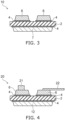
- FIG. 3 is a schematic view showing an example of a ceramic-copper circuit board according to an embodiment.
- 6 is a circuit part
- 7 is a heat dissipation plate
- 10 is a ceramic-copper circuit board.
- the circuit part 6 is made by providing a circuit structure in the copper plate 3 at the front side.
- the heat dissipation plate 7 is made by patterning the copper plate 3 at the backside.
- the structure of FIG. 3 includes two circuit parts 6, the structure is not limited to such a structure. Any number or shape of the circuit parts 6 can be provided.
- the copper plates 3 of two surfaces may be used as the circuit parts 6.
- the side surfaces of the circuit part 6 and/or the heat dissipation plate 7 may have inclined structures.
- a bonding layer jutting portion in which the bonding layer 4 juts from the end portions of the circuit part 6 and/or the heat dissipation plate 7 may be provided.
- FIG. 4 is a schematic view showing an example of a semiconductor device according to an embodiment.
- 20 is a semiconductor device
- 21 is a semiconductor element
- 22 is a leadframe.
- the semiconductor element 21 is mounted to one of the two circuit parts 6.
- the leadframe 22 is connected to the other of the two circuit parts 6.
- the semiconductor device 20 according to the embodiment is not limited to such a structure. As necessary, the number and sizes of the circuit parts 6, the number and sizes of the semiconductor elements 21, etc., are modifiable as appropriate.
- a method for manufacturing the bonded body according to the embodiment will now be described.
- the manufacturing method is not limited as long as the bonded body according to the embodiment has the configuration described above.
- a method for obtaining the bonded body according to the embodiment with a high yield will now be described.
- the ceramic substrate 2 is prepared.
- a silicon nitride substrate, an aluminum nitride substrate, an aluminum oxide substrate, an Alusil substrate, etc., are examples of the ceramic substrate 2.
- a copper plate or a copper alloy plate can be used as the copper plate 3. It is favorable for the copper plate to be an oxygen-free copper plate. Oxygen-free copper is copper that has a copper purity of not less than 99.96 mass% as indicated in JIS-H-3100. Also, it is favorable for the average crystal grain size of the copper crystal of the copper plate before bonding to be in the range of not less than 5 ⁇ m and not more than 100 ⁇ m. The average crystal grain size of the copper crystal is calculated using the line intercept method. The copper crystals are counted along a 10-mm straight line at any location of the copper plate front surface; and the average crystal grain size of the crystals is calculated. The grain boundaries of the copper crystals are the main route along which Ag diffuses.
- the Ag diffusion amount increases too much when the average crystal grain size of the copper plate is less than 5 ⁇ m. Also, the Ag diffusion amount decreases when the average crystal grain size of the copper plate is large and is greater than 100 ⁇ m. It is therefore favorable for the average crystal grain size of the copper plate before bonding to be not less than 5 ⁇ m and not more than 100 ⁇ m, and more favorably not less than 10 ⁇ m and not more than 50 ⁇ m.
- an active metal brazing material paste that includes Ag and Ti is prepared. It is favorable for one, two, or more selected from Cu, Sn, In, and C to be added to the active metal brazing material including Ag and Ti. Ti may be added as a compound of TiH 2 , etc.
- the composition ratios of the components (mass%) are as described above.
- the average particle size D 50 of the Ag powder used as the raw material of the brazing material is not more than 3.0 ⁇ m, and more favorably not more than 2.0 ⁇ m. It is favorable for the average particle size D 50 of the Cu powder to be not more than 6.0 ⁇ m, and more favorably not more than 4.0 ⁇ m. It is favorable for the average particle size D 50 of the Ti powder or the TiH 2 powder to be not more than 6.0 ⁇ m, and more favorably not more than 4.0 ⁇ m. It is favorable for the average particle size D 50 of the Sn powder or the In powder to be not more than 6.0 ⁇ m, and more favorably not more than 4.0 ⁇ m. It is favorable for the average particle size D 50 of the C powder to be not more than 6.0 ⁇ m, and more favorably not more than 4.0 ⁇ m.
- the average particle size D 50 of the Ag powder is favorable for the average particle size D 50 of the Ag powder to be less than the average particle size D 50 of the Cu powder. It is favorable for the average particle size D 50 of the Ag powder to be less than the average particle size D 50 of the Sn powder or the In powder. It is favorable for the average particle size D 50 of the Cu powder to be less than the average particle size D 50 of the Sn powder or the In powder. By reducing the particle size of the Ag powder, the Ag easily diffuses into the copper plate.
- a mixed powder is prepared by mixing and uniformly dispersing the constituent component powders of the active metal brazing material. It is favorable for the mixing time to be not less than 10 hours.
- an active metal brazing material paste is prepared by mixing the mixed powder with a binder and a solvent.
- the active metal brazing material paste is coated onto at least one of the ceramic substrate or the copper plate. It is favorable for the thickness of the active metal brazing material paste layer to be not less than 5 ⁇ m and not more than 60 ⁇ m.
- the thickness of the active metal brazing material paste layer is the thickness after drying the coated paste. There is a possibility that the bonding strength may decrease when the thickness of the active metal brazing material paste layer is less than 5 ⁇ m.
- the thickness of the active metal brazing material paste layer is not less than 5 ⁇ m and not more than 60 ⁇ m, and more favorably not less than 10 ⁇ m and not more than 50 ⁇ m.
- the active metal brazing material paste After the active metal brazing material paste is coated, a process of placing the component on which the paste is not coated is performed. For example, when the active metal brazing material paste is coated onto the ceramic substrate, a process of placing the copper plate on the ceramic substrate is performed.
- the active metal brazing material paste may be coated onto two surfaces of the ceramic substrate; and the copper plates may be disposed respectively on the two surfaces.
- An active metal brazing material paste may be coated onto the copper plate; and a ceramic substrate may be disposed on the copper plate.
- the bonding temperature is the maximum attained temperature maintained for a certain amount of time.
- the bonding temperature is high, the grain growth of the copper crystal grains included in the copper plate is promoted.
- the diffusion amount of Ag decreases when the grain growth of the copper plate is fast.
- the bonding temperature is not more than 900 °C, and more favorably not more than 860 °C. Although not particularly limited, it is favorable for the lower limit of the bonding temperature to be not less than 500 °C. When the bonding temperature is low, there is a possibility that the reliability of the bond may degrade. It is therefore favorable for the bonding temperature to be not less than 500 °C and not more than 900 °C, and more favorably not less than 550 °C and not more than 860 °C. It is favorable for the holding time of the bonding temperature to be not more than 100 minutes, and more favorably not more than 30 minutes.
- the atmosphere in the bonding process is a vacuum or a nitrogen atmosphere.
- the pressure of the vacuum is not more than 10 -3 Pa.
- the Ti inside the brazing material can be prevented from nitriding before reacting with the ceramic substrate.
- a nitrogen atmosphere is an atmosphere that includes not less than 90 vol% of nitrogen. It is considered that Ti becomes TiN (titanium nitride) before reacting with the ceramic substrate when nitrogen is present in the atmosphere in the bonding process. When the Ti content inside the brazing material is not less than 6 mass%, the Ti and the ceramic substrate can sufficiently react even in a nitrogen atmosphere.
- the bonding process may be performed using either a batch or continuous technique.
- a batch technique the ceramic substrate and the copper plate are placed in a storage container, and heat treatment is performed.
- a continuous technique the ceramic substrate and the copper plate are placed on a belt conveyor, and heat treatment is performed while moving.
- the batch technique is suited to the bonding process in a vacuum.
- the continuous technique is suited to the bonding process in a nitrogen atmosphere.
- the cooling rate from the bonding temperature is not more than 50 °C/minute.
- the Ag diffusion into the copper plate is promoted by the heat in the bonding process.
- the diffusion rate of Ag can be reduced by holding at the bonding temperature and then cooling at a slow rate of not more than 50 °C/minute. Thereby, a region that has a high Ag concentration can be formed inside the copper plate.
- the Ag concentration in the copper plate can be controlled by controlling the grain size of the copper crystal of the copper plate before bonding, the Ag grain size inside the brazing material, the cooling rate after bonding, etc.
- a bonded body in which the Ag concentration in the copper plate is controlled has excellent TCT characteristics.
- the warp amount of the bonded body can be not more than 0.1 mm even when the size of the bonded body is large, i.e., not less than 200 mm long or wide.
- Multi-part manufacturing is a method of obtaining small bonded bodies by subdividing a large bonded body. Laser scribing or the like may be performed to make the subdividing easy. According to the embodiment, a bonded body that is suited to multi-part manufacturing can be provided because the bonded body can be enlarged.
- the ceramic-copper circuit board 10 can be manufactured by providing the structures of the circuit part 6 and the heat dissipation plate 7 in the copper plate 3 of the obtained bonded body 1.
- An etching process is effective for providing the circuit part 6 or the heat dissipation plate 7 with a structure.
- the side surface of the circuit part 6 or the heat dissipation plate 7 may be provided with an inclined shape.
- the bonding layer 4 may be provided with a jutting portion jutting from the end portion of the circuit part 6 or the heat dissipation plate 7.
- the silicon nitride substrates shown in Table 1 were prepared as ceramic substrates.
- the active metal brazing material pastes were prepared, and bonded bodies were made.
- the silicon nitride substrates, active metal brazing materials, copper plates, and bonding processes were as shown in Table 4. The bonding was performed in a vacuum of not more than 10 -3 Pa.
- the Ag concentration in the copper plate was checked for the obtained bonded bodies.
- the analysis of the Ag concentration was performed by measuring the copper plate in an arbitrary cross section of the bonded body with EDX.
- JED-2300 made by JEOL Ltd. was used as the SEM-EDX.
- the EDX measurement regions were unified to 200 ⁇ m in the width directionx50 ⁇ m in the thickness direction.
- the spacing P between the measurement regions was unified to 50 ⁇ m.
- Eight locations of measurement regions were set for bonded bodies having the copper plate thicknesses of 0.8 mm.
- Ten locations of measurement regions were set for bonded bodies having copper plate thicknesses of 1.0 mm. Based on the EDX measurement results, it was checked whether or not a Ag concentration distribution existed inside the copper plate 3 in which a region having a relatively low Ag concentration, a region having a relatively high Ag concentration, and a region having a relatively low Ag concentration were arranged in this order.
- the high-concentration region existed in the Ag concentration distribution within a range of not less than 0.1 mm and not more than 0.5 mm from the boundary between the bonding layer and the copper plate. Also, the Ag concentration (atomic%) of the high-concentration region was determined.
- the warp amounts of the bonded bodies were measured.
- the warp amount of the long side was measured as the warp amount of the bonded body.
- Bonded bodies of which the warp amount was not more than 0.2 mm were displayed as good (circle); and bonded bodies of which the warp amount was greater than 0.2 mm were displayed as no-good (cross).
- a Ag concentration distribution exists in a portion of the copper plate for the bonded bodies according to the examples.
- the high-concentration region inside the Ag concentration distribution was within the range of not less than 0.1 mm and not more than 0.5 mm from the boundary between the bonding layer and the copper plate.
- the Ag concentration of the high-concentration region was within the range of 0.1 to 0.4 atomic%.
- the Ag concentration difference between the high-concentration region and the low-concentration region was not less than 0.05 atomic%.
- the warp amount of the bonded body was a small value of not more than 0.2 mm.
- the bonded bodies according to the comparative examples a portion does not exist inside the copper plate in which a region having a relatively low Ag concentration, a region having a relatively high Ag concentration, and a region having a relatively low Ag concentration were arranged in this order.
- the Ag concentration gradually decreased from the bonding layer side toward the copper plate front surface.
- the warp amounts of the bonded bodies were greater than 0.2 mm.
- the grain size of the copper crystal of the copper plate, the Ag grain size of the brazing material, the cooling rate of the bonding process, etc. are effective to control the Ag concentration. Also, according to the embodiment, it was found that the warp amount can be reduced even when the long side of the bonded body is enlarged to be not less than 200 mm.
- the bonded body was patterned by etching to provide the copper plate of the front side with a circuit part structure, and to provide the copper plate of the backside with a heat dissipation plate structure.
- Multi-part manufacturing was used to make four ceramic-copper circuit boards by scribing the bonded body.
- the TCT test was performed by using -40 °C ⁇ 30 minutes - > room temperaturex10 minutes -> 170 °C ⁇ 30 minutes -> room temperaturex10 minutes as 1 cycle, and by performing tests of 1500 cycles and 2500 cycles.
- the cases where no discrepancies occurred for any of the four were set to best (double circle), the cases where a discrepancy occurred in one were set to good (circle), and the cases where discrepancies occurred in two or more were set to no-good (cross).
- the TCT characteristics were good for the ceramic-copper circuit boards according to the examples. It was found that the TCT characteristics can be improved by controlling the Ag concentration in the copper plate.
- the Ag concentration difference between the high-concentration region and the low-concentration region was within the range of not less than 0.05 atomic% and not more than 0.4 atomic%.
- the Ag concentration difference between the high-concentration region and the low-concentration region was 0.02 atomic%. It was found that the TCT characteristics slightly degraded when the Ag concentration difference was small.
Landscapes
- Chemical & Material Sciences (AREA)
- Engineering & Computer Science (AREA)
- Ceramic Engineering (AREA)
- Microelectronics & Electronic Packaging (AREA)
- Materials Engineering (AREA)
- Structural Engineering (AREA)
- Organic Chemistry (AREA)
- Inorganic Chemistry (AREA)
- Ceramic Products (AREA)
Abstract
Description
- Embodiments described below relate generally to a bonded body, a ceramic-copper circuit board, and a semiconductor device.
- A bonded body of a ceramic substrate and a copper plate is used as a circuit board for mounting a semiconductor element or the like.
WO 2018/180965 (Patent Document 1) discusses a ceramic-copper circuit board in which a ceramic substrate and a copper plate are bonded. InPatent Document 1, the crystal grain size of the copper plate and the diffusion amount of Ag inside the copper plate are controlled. By performing such a control inPatent Document 1, the temperature cycle test (TCT) characteristics of the ceramic-copper circuit board are improved. - On the other hand, as ceramic-copper circuit board sizes increase, there are ceramic-copper circuit boards in which the TCT characteristics are not improved.
- Patent Document 1:
WO 2018/180965 - By investigating the cause, it was found that the diffusion amount of Ag into the copper plate is a cause. In
Patent Document 1, the diffusion amount of Ag is controlled by uniformly trisecting the copper plate in the thickness direction. The Ag diffusion amount is reduced from the vicinity of the bonding layer toward the copper plate front surface. The Ag inside the copper plate diffuses from the bonding layer. Therefore, the Ag amount was high at locations proximate to the bonding layer; and the Ag amount decreased toward the copper plate front surface. A thermal expansion difference occurs between high and low diffusion amounts of Ag in the copper plate. It was found that this partial difference of the diffusion amount of Ag is the cause of the inhibition of the improvement of the TCT characteristics. - An object of the invention is to address such problems and to provide a bonded body in which the Ag concentration in the copper plate is controlled.
- A bonded body according to an embodiment includes a ceramic substrate, a copper plate, and a bonding layer. The bonding layer is located on at least one surface of the ceramic substrate and bonds the ceramic substrate and the copper plate. The bonding layer includes Ag and Ti. The copper plate includes a first region, a second region, and a third region. The first region is separated from the bonding layer in a thickness direction. The second region is located between the bonding layer and the first region and has a higher Ag concentration than the first region. The third region is located between the bonding layer and the second region and has a lower Ag concentration than the second region.
-
- [
FIG. 1 ]
FIG. 1 is a schematic view showing an example of a bonded body according to an embodiment. - [
FIG. 2 ]
FIG. 2 is a schematic view showing an example of a measurement region measuring the Ag concentration in a copper plate. - [
FIG. 3 ]
FIG. 3 is a schematic view showing an example of a ceramic-copper circuit board according to an embodiment. - [
FIG. 4 ]
FIG. 4 is a schematic view showing an example of a semiconductor device according to an embodiment. - A bonded body according to an embodiment includes a ceramic substrate, a copper plate, and a bonding layer. The bonding layer is located on at least one surface of the ceramic substrate and bonds the ceramic substrate and the copper plate. The bonding layer includes Ag and Ti. The copper plate includes a first region, a second region, and a third region. The first region is separated from the bonding layer in a thickness direction. The second region is located between the bonding layer and the first region and has a higher Ag concentration than the first region. The third region is located between the bonding layer and the second region and has a lower Ag concentration than the second region.
-
FIG. 1 is a schematic view showing an example of a bonded body according to an embodiment. InFIG. 1, 1 is a bonded body, 2 is a ceramic substrate, 3 is a copper plate, and 4 is a bonding layer. -
FIG. 1 shows thebonded body 1 in which thecopper plate 3 is located at each of two surfaces of theceramic substrate 2 with thebonding layers 4 interposed. In the example shown inFIG. 1 , the longitudinal and lateral sizes of theceramic substrate 2 are equal to the longitudinal and lateral sizes of thecopper plate 3. The bonded body according to the embodiment is not limited to such a configuration. Thebonded body 1 may have a structure in which the copper plate is located at only one surface of thebonded body 1. The longitudinal and lateral sizes of theceramic substrate 2 may be different from the longitudinal and lateral sizes of thecopper plate 3. -
FIG. 2 is a schematic view showing an example of a measurement region measuring the Ag concentration in a copper plate. InFIG. 2 ,3 is a copper plate, 4 is a bonding layer, 5 is a measurement region, T is the thickness of the copper plate, and P is the spacing (pitch) between the measurement regions. 5-1 is a first measurement region, 5-2 is a second measurement region, 5-3 is a third measurement region, 5-4 is a fourth measurement region, 5-5 is a fifth measurement region, 5-6 is a sixth measurement region, 5-7 is a seventh measurement region, and 5-n is an nth measurement region, n examples of the measurement region are shown inFIG. 2 . - First, any cross section of the
bonded body 1 is set as the location to be measured. The cross section is a surface perpendicular to the direction connecting theceramic substrate 2 and thecopper plate 3. That is, the cross section is a surface perpendicular to the bonding surface of theceramic substrate 2 and thecopper plate 3. - Then, the pitch P of the multiple measurement regions is determined. The multiple measurement regions are arranged at uniform spacing at a pitch of not less than 30 µm and not more than 100 µm in the thickness direction of the
copper plate 3. The pitch is the spacing P between the centers of the measurement regions arranged vertically. The spacing P between the centers of the measurement regions also is called the pitch P. The pitch P is a constant spacing within the range of 30 to 100 µm. For example, when the pitch P is set to be 50 µm, the pitch P is always 50 µm. Also, when the pitch P is set to be 100 µm, the pitch P is always 100 µm. - The length in the width direction of one
measurement region 5 is within the range of not less than 100 µm and not more than 200 µm. The length in the thickness direction of onemeasurement region 5 is within the range of not less than 10 µm and not more than 100 µm. Themeasurement region 5 is a quadrilateral defined by the width directionxthickness direction. The width direction is a direction parallel to theceramic substrate 2 surface. That is, the width direction is a direction parallel to thecopper plate 3 surface. The thickness direction is a direction perpendicular to theceramic substrate 2 surface, and is the thickness direction of thecopper plate 3. Themeasurement regions 5 are arranged in the thickness direction of thecopper plate 3. - One size is selected as the size of each
measurement region 5 from the range of not less than 100 µm and not more than 200 µm in the width directionxnot less than 10 µm and not more than 100 µm in the thickness direction. For example, when the size of themeasurement region 5 is set to be 150 µm in the width directionx50 µm in the thickness direction, the sizes of all of themeasurement regions 5 are 150 µm in the width directionx50 µm in the thickness direction. - When the size of the
measurement region 5 has been determined, the measurement regions are designated to match the pitch P described above. The pitch P is counted from the bonding surface of thecopper plate 3. Positioning is performed to be alternately pitch P -> measurement region 5 -> pitch P ->measurement region 5. InFIG. 2 , the measurement region that is most proximate to thebonding layer 4 is set as the first measurement region 5-1. The measurement region that is most distant to thebonding layer 4 is set as the nth measurement region 5-n. - When the
measurement regions 5 have been set, the Ag concentrations of themeasurement regions 5 are measured using energy dispersive X-ray spectroscopy (EDX). EDX also is called EDS. The Ag concentration is measured for each measurement region. Therefore, the Ag concentrations of the n measurement regions including the first to nth measurement regions 5-1 to 5-n are measured. - A Scanning Electron Microscope (SEM)-EDX is used to measure the Ag concentrations. JED-2300 made by JEOL Ltd. or a device having equivalent performance is used as the SEM-EDX. The Ag concentration is measured as atomic% to two decimal places. Also, the time for the peaks to stabilize in the EDX measurement is recorded. Field Emission (FE)-SEM may be used as SEM.
- The
copper plate 3 is characterized in that thecopper plate 3 includes a portion in which a region having a relatively low Ag concentration, a region having a relatively high Ag concentration, and a region having a relatively low Ag concentration are arranged in this order from theceramic substrate 2 side toward the side opposite to theceramic substrate 2 side. The direction from theceramic substrate 2 side toward the side opposite to theceramic substrate 2 side is the so-called thickness direction of thecopper plate 3. That is, this direction is a direction from thebonding layer 4 toward thecopper plate 3 surface. - For example, the
copper plate 3 includes the first region, the second region, and the third region. The first region is separated from thebonding layer 4 in the thickness direction. The second region is positioned between the bonding layer and the first region and has a higher Ag concentration than the first region. The third region is positioned between the bonding layer and the second region and has a lower Ag concentration than the second region. The first region is positioned at the front side of thecopper plate 3 when viewed from the second and third regions. - The first to third regions are a portion of the multiple measurement regions and are next to each other in the thickness direction. Therefore, the first to third regions are arranged at a pitch of not less than 30 µm and not more than 100 µm in the thickness direction. The sizes of the first to third regions each are not less than 100 µm and not more than 200 µm in the width directionxnot less than 10 µm and not more than 100 µm in the thickness direction.
- As described above, a region having a relatively low Ag concentration, a region having a relatively high Ag concentration, and a region having a relatively low Ag concentration are arranged in this order in a portion of the
copper plate 3. This means that when the Ag concentrations of the measurement regions are compared in order from thebonding layer 4 toward thecopper plate 3 surface, there exists a location made of a region having a relatively low Ag concentration, a region having a relatively high Ag concentration, and a region having a relatively low Ag concentration. Suppose, for example, thatmultiple measurement regions 5 that include the first to nth measurement regions 5-1 to 5-n are set. Among the first to nth measurement regions 5-1 to 5-n, there exists three measurement regions arranged in the order of a region having a relatively low Ag concentration -> a region having a relatively high Ag concentration -> a region having a relatively low Ag concentration in the direction from thebonding layer 4 toward thecopper plate 3 surface. Hereinafter, the region having the relatively high Ag concentration (the second region) also is called the "high-concentration region". The region having the relatively low Ag concentration (the first region and the third region) also is called the "low-concentration region". - Conventionally, the diffusion amount of Ag into the copper plate decreases from the bonding layer toward the copper plate front surface. Therefore, when comparing the Ag concentrations of the measurement regions arranged in order, the Ag concentration is arranged in the order of high -> low -> lower. Conversely, at a portion of the
copper plate 3 in the bondedbody 1 according to the embodiment, the region having the relatively low Ag concentration -> region having the relatively high Ag concentration -> region having the relatively low Ag concentration are arranged in this order. It is sufficient for at least one area including such a Ag concentration undulation made of the three regions to exist. Two or more areas having Ag concentration undulations may be included in thecopper plate 3. Favorably, only one such area is included in thecopper plate 3. - When n measurement regions including the first to nth measurement regions 5-1 to 5-n are set, for example, an area that includes the first measurement region 5-1, the second measurement region 5-2, and the third measurement region 5-3 includes a Ag concentration undulation. The third measurement region 5-3 corresponds to the above-mentioned first region. The second measurement region 5-2 corresponds to the above-mentioned second region. The first measurement region 5-1 corresponds to the above-mentioned third region. Or, one of an area including the second measurement region 5-2, the third measurement region 5-3, and the fourth measurement region 5-4, an area including the third measurement region 5-3, the fourth measurement region 5-4, and the fifth measurement region 5-5, an area including the fourth measurement region 5-4, the fifth measurement region 5-5, and the sixth measurement region 5-6, or an area including the fifth measurement region 5-5, the sixth measurement region 5-6, and the seventh measurement region 5-7 may include a Ag concentration undulation. Two or more of these areas may include Ag concentration undulations.
- Also, the copper plate front surface is not included in a measurement region. Therefore, a location that is separated not less than 30 µm from the copper plate front surface is used as the nth measurement region. The separation of not less than 30 µm is because the pitch P is not less than 30 µm and not more than 100 µm. Ag may be detected or may not be detected at the copper plate front surface.
- Thus, it is important for an area including a Ag concentration undulation to exist, and for the
copper plate 3 to have a Ag concentration distribution. By thecopper plate 3 having a Ag concentration distribution, the TCT characteristics of the bonded body and the ceramic-copper circuit board can be improved. The existence of an area that includes a Ag concentration undulation means that a high-concentration region exists inside the copper plate when the copper plate is viewed in the thickness direction. Ag mainly exists at the grain boundaries of the copper crystals of the copper plate. By Ag existing at the grain boundaries of the copper crystals, the thermal expansion of the copper plate can be suppressed by a pinning effect. Therefore, the TCT characteristics can be improved. Also, by forming a low-concentration region between the bonding layer and the high-concentration region, the thermal expansion can be suppressed while leveraging the thermal conductivity and electrical conductivity of the copper plate. For example, the warp amount of the bonded body can be not more than 0.2 mm even when the bonded body size becomes large, i.e., not less than 200 mm long or wide. Whether or not Ag exists at the grain boundaries of the copper plate can be known by combining a SEM photograph with component analysis by SEM-EDX. First, the location of a grain boundary of the copper plate is designated using a SEM photograph. Whether or not Ag exists at the grain boundary of the copper plate can be confirmed by analyzing the location identified by the SEM photograph with EDX. - It is favorable for the high-concentration region (the second region) to exist within the range of not less than 0.1 mm and not more than 0.5 mm. The range of not less than 0.1 mm and not more than 0.5 mm is the distance referenced to the boundary between the bonding layer and the copper plate. "0.1 mm" is a position more proximate to the
bonding layer 4. "0.5 mm" is near the thickness-direction center of thecopper plate 3. The thermal expansion of the copper plate can be suppressed by forming the high-concentration region between thebonding layer 4 and the central portion of thecopper plate 3. Also, it is favorable for the high-concentration region to exist in the range of 0.3T to 0.5T with respect to the thickness T of the copper plate. The boundary of thecopper plate 3 and thebonding layer 4 is defined using a location at which the Ag amount is 5 atomic% as a reference. The Ag inside the bonding layer diffuses into the copper plate. The Ag amount decreases from the bonding layer toward the copper plate. The location from the bonding layer toward the copper plate at which the Ag amount becomes 5 atomic% is defined as the boundary of thecopper plate 3 and thebonding layer 4. - It is favorable for the Ag concentration of the high-concentration region to be not less than 0.1 atomic% when the total concentration of Ag and Cu is taken to be 100 atomic%. In other words, it is favorable for 0.1 ≥ /CAg (CAg + CCu ), where CAg is the actual Ag concentration (atomic%) in the high-concentration region, and CCu is the actual Cu concentration (atomic%) in the high-concentration region. Also, it is favorable for the Ag concentration of the high-concentration region to be not more than 0.4 atomic% when the total concentration of Ag and Cu is taken to be 100 atomic%. There is a possibility that the goodness of the copper plate (the thermal conductivity and the electrical conductivity) may not be leveraged if the Ag concentration in the copper plate becomes too high.
- It is favorable for the difference between the Ag concentration of the low-concentration region and the Ag concentration of the high-concentration region to be not less than 0.05 atomic% when the total concentration of Ag and Cu is taken to be 100 atomic%. The effects can be improved by setting the Ag concentration difference to be not less than 0.05 atomic%.
- It is favorable for the thickness T of the
copper plate 3 to be not less than 0.8 mm. The deformation amount due to thermal expansion increases when thecopper plate 3 is thick. However, the thermal expansion can be suppressed by controlling the Ag concentration. - A pure copper plate or a copper alloy plate can be used as the
copper plate 3. It is favorable for the copper plate to be oxygen-free copper. Oxygen-free copper is one type of pure copper. Oxygen-free copper is copper having a copper purity of not less than 99.96 mass% as indicated in JIS-H-3100 (ISO 1337, etc.). - A silicon nitride substrate, an aluminum nitride substrate, an aluminum oxide substrate, an Alusil substrate, etc., are examples of the
ceramic substrate 2. An Alusil substrate is a substrate formed by mixing aluminum oxide and zirconium oxide. - It is favorable for the thickness of the
ceramic substrate 2 to be not less than 0.1 mm and not more than 1 mm. There is a possibility that the strength may degrade when the substrate thickness is less than 0.1 mm. When the thickness is greater than 1 mm, there is a possibility that the ceramic substrate may become a thermal resistor, and the heat dissipation of the bonded body may degrade. - It is favorable for the three-point bending strength of the silicon nitride substrate to be not less than 600 MPa. It is favorable for the thermal conductivity to be not less than 80 W/m·K. The substrate thickness can be thinned by increasing the strength of the silicon nitride substrate. It is therefore favorable for the three-point bending strength of the silicon nitride substrate to be not less than 600 MPa, or even not less than 700 MPa. The substrate thickness of the silicon nitride substrate can be thin, i.e., not more than 0.40 mm, or even not more than 0.30 mm.
- The three-point bending strength of an aluminum nitride substrate is about 300 to 450 MPa. On the other hand, the thermal conductivity of an aluminum nitride substrate is not less than 160 W/m·K. Because the strength of the aluminum nitride substrate is low, it is favorable for the substrate thickness to be not less than 0.60 mm.
- Although the three-point bending strength of an aluminum oxide substrate is about 300 to 450 MPa, an aluminum oxide substrate is inexpensive. Although the three-point bending strength of an Alusil substrate is high, i.e., about 550 MPa, the thermal conductivity of an Alusil substrate is about 30 to 50 W/m·K.
- A silicon nitride substrate is favorable as the
ceramic substrate 2. As described above, the substrate thickness can be thin because the strength of the silicon nitride substrate is high. The thermal resistance of the ceramic substrate can be reduced thereby. - The
bonding layer 4 includes Ag and Ti. Ti (titanium) is an element that is called an active metal. A bonding method of the ceramic substrate and the copper plate that uses an active metal is called active metal bonding. The bonding layer that includes Ag and Ti is formed using a brazing material including Ag and Ti. A brazing material that includes Ti is called an active metal brazing material. The active metal brazing material also is called simply the brazing material. - By the
bonding layer 4 including Ag (silver), the Ag can diffuse into thecopper plate 3. The Ag concentration in thecopper plate 3 can be controlled by utilizing the diffusion of Ag. Although it also may be considered to use a copper plate that already includes Ag, in such a case, the Ag concentration easily becomes uniform, and it is difficult to control the distribution of the Ag concentration. - In addition to Ag and Ti, it is favorable for the
bonding layer 4 to include one, two, or more selected from Cu, Sn, In, and C. - It is favorable for the active metal brazing material to include not less than 20 mass% and not more than 60 mass% of Ag (silver), not less than 25 mass% and not more than 70 mass% of Cu (copper), and not less than 1 mass% and not more than 15 mass% of Ti (titanium) or TiH2 (titanium hydride). Also, when both Ti and TiH2 are used, the total of the two is set within the range of 1 to 15 mass%.
- The brazing material may include not less than 1 mass% and not more than 50 mass% of one or two of Sn (tin) or In (indium) as necessary. It is favorable for the content of Ti or TiH2 to be 1 to 15 mass%. The brazing material may include not less than 0.1 mass% and not more than 2 mass% of C (carbon) as necessary.
- The ratio of the active metal brazing material composition is calculated using the total of the mixed raw materials as 100 mass%. For example, when the three of Ag, Cu, and Ti are used in the brazing material, Ag + Cu + Ti = 100 mass%. When the four of Ag, Cu, TiH2, and In are used in the brazing material, Ag + Cu + TiH2 + In = 100 mass%. When the five of Ag, Cu, Ti, Sn, and C are included in the
bonding layer 4, Ag + Cu + Ti + Sn + C = 100 mass%. - Ag or Cu is a component used as the base material of the brazing material. Sn or In has the effect of lowering the melting point of the brazing material. C (carbon) has the effect of controlling the fluidity of the brazing material and controlling the composition of the bonding layer by reacting with other components. Therefore, Ag-Cu-Ti, Ag-Cu-Sn-Ti, Ag-Cu-Ti-C, Ag-Cu-Sn-Ti-C, Ag-Ti, Ag-Sn-Ti, Ag-Ti-C, and Ag-Sn-Ti-C are examples of the components of the brazing material. Also, In may be used instead of Sn. Also, both Sn and In may be used. Also, low melting-point metals such as Bi (bismuth), Sb (antimony), Ga (gallium), etc., may be used instead of Sn and In.
- The bonded body described above is favorable for a ceramic-copper circuit board.
FIG. 3 is a schematic view showing an example of a ceramic-copper circuit board according to an embodiment. InFIG. 3 , 6 is a circuit part, 7 is a heat dissipation plate, and 10 is a ceramic-copper circuit board. - The
circuit part 6 is made by providing a circuit structure in thecopper plate 3 at the front side. Also, theheat dissipation plate 7 is made by patterning thecopper plate 3 at the backside. Although the structure ofFIG. 3 includes twocircuit parts 6, the structure is not limited to such a structure. Any number or shape of thecircuit parts 6 can be provided. Also, thecopper plates 3 of two surfaces may be used as thecircuit parts 6. Also, the side surfaces of thecircuit part 6 and/or theheat dissipation plate 7 may have inclined structures. Also, a bonding layer jutting portion in which thebonding layer 4 juts from the end portions of thecircuit part 6 and/or theheat dissipation plate 7 may be provided. - The ceramic-copper circuit board according to the embodiment is favorable for a semiconductor device.
FIG. 4 is a schematic view showing an example of a semiconductor device according to an embodiment. InFIG. 4 , 20 is a semiconductor device, 21 is a semiconductor element, and 22 is a leadframe. In thesemiconductor device 20 shown in FIG. 5, thesemiconductor element 21 is mounted to one of the twocircuit parts 6. Theleadframe 22 is connected to the other of the twocircuit parts 6. Thesemiconductor device 20 according to the embodiment is not limited to such a structure. As necessary, the number and sizes of thecircuit parts 6, the number and sizes of thesemiconductor elements 21, etc., are modifiable as appropriate. - A method for manufacturing the bonded body according to the embodiment will now be described. The manufacturing method is not limited as long as the bonded body according to the embodiment has the configuration described above. A method for obtaining the bonded body according to the embodiment with a high yield will now be described.
- First, the
ceramic substrate 2 is prepared. A silicon nitride substrate, an aluminum nitride substrate, an aluminum oxide substrate, an Alusil substrate, etc., are examples of theceramic substrate 2. - A copper plate or a copper alloy plate can be used as the
copper plate 3. It is favorable for the copper plate to be an oxygen-free copper plate. Oxygen-free copper is copper that has a copper purity of not less than 99.96 mass% as indicated in JIS-H-3100. Also, it is favorable for the average crystal grain size of the copper crystal of the copper plate before bonding to be in the range of not less than 5 µm and not more than 100 µm. The average crystal grain size of the copper crystal is calculated using the line intercept method. The copper crystals are counted along a 10-mm straight line at any location of the copper plate front surface; and the average crystal grain size of the crystals is calculated. The grain boundaries of the copper crystals are the main route along which Ag diffuses. The Ag diffusion amount increases too much when the average crystal grain size of the copper plate is less than 5 µm. Also, the Ag diffusion amount decreases when the average crystal grain size of the copper plate is large and is greater than 100 µm. It is therefore favorable for the average crystal grain size of the copper plate before bonding to be not less than 5 µm and not more than 100 µm, and more favorably not less than 10 µm and not more than 50 µm. - Then, an active metal brazing material paste that includes Ag and Ti is prepared. It is favorable for one, two, or more selected from Cu, Sn, In, and C to be added to the active metal brazing material including Ag and Ti. Ti may be added as a compound of TiH2, etc. The composition ratios of the components (mass%) are as described above.
- It is favorable for the average particle size D50 of the Ag powder used as the raw material of the brazing material to be not more than 3.0 µm, and more favorably not more than 2.0 µm. It is favorable for the average particle size D50 of the Cu powder to be not more than 6.0 µm, and more favorably not more than 4.0 µm. It is favorable for the average particle size D50 of the Ti powder or the TiH2 powder to be not more than 6.0 µm, and more favorably not more than 4.0 µm. It is favorable for the average particle size D50 of the Sn powder or the In powder to be not more than 6.0 µm, and more favorably not more than 4.0 µm. It is favorable for the average particle size D50 of the C powder to be not more than 6.0 µm, and more favorably not more than 4.0 µm.
- It is favorable for the average particle size D50 of the Ag powder to be less than the average particle size D50 of the Cu powder. It is favorable for the average particle size D50 of the Ag powder to be less than the average particle size D50 of the Sn powder or the In powder. It is favorable for the average particle size D50 of the Cu powder to be less than the average particle size D50 of the Sn powder or the In powder. By reducing the particle size of the Ag powder, the Ag easily diffuses into the copper plate.
- A mixed powder is prepared by mixing and uniformly dispersing the constituent component powders of the active metal brazing material. It is favorable for the mixing time to be not less than 10 hours. Then, an active metal brazing material paste is prepared by mixing the mixed powder with a binder and a solvent. The active metal brazing material paste is coated onto at least one of the ceramic substrate or the copper plate. It is favorable for the thickness of the active metal brazing material paste layer to be not less than 5 µm and not more than 60 µm. The thickness of the active metal brazing material paste layer is the thickness after drying the coated paste. There is a possibility that the bonding strength may decrease when the thickness of the active metal brazing material paste layer is less than 5 µm. When the active metal brazing material paste layer is thick, i.e., greater than 60 µm, there is a possibility that the thermal stress in the bonding process may become large, and the warp of the bonded body may become large. It is therefore favorable for the thickness of the active metal brazing material paste layer to be not less than 5 µm and not more than 60 µm, and more favorably not less than 10 µm and not more than 50 µm.
- After the active metal brazing material paste is coated, a process of placing the component on which the paste is not coated is performed. For example, when the active metal brazing material paste is coated onto the ceramic substrate, a process of placing the copper plate on the ceramic substrate is performed. The active metal brazing material paste may be coated onto two surfaces of the ceramic substrate; and the copper plates may be disposed respectively on the two surfaces. An active metal brazing material paste may be coated onto the copper plate; and a ceramic substrate may be disposed on the copper plate.
- Then, a bonding process in which the bonding temperature is not more than 900 °C is performed. The bonding temperature is the maximum attained temperature maintained for a certain amount of time. When the bonding temperature is high, the grain growth of the copper crystal grains included in the copper plate is promoted. The diffusion amount of Ag decreases when the grain growth of the copper plate is fast.
- It is favorable for the bonding temperature to be not more than 900 °C, and more favorably not more than 860 °C. Although not particularly limited, it is favorable for the lower limit of the bonding temperature to be not less than 500 °C. When the bonding temperature is low, there is a possibility that the reliability of the bond may degrade. It is therefore favorable for the bonding temperature to be not less than 500 °C and not more than 900 °C, and more favorably not less than 550 °C and not more than 860 °C. It is favorable for the holding time of the bonding temperature to be not more than 100 minutes, and more favorably not more than 30 minutes.
- It is favorable for the atmosphere in the bonding process to be a vacuum or a nitrogen atmosphere.
- It is favorable for the pressure of the vacuum to be not more than 10-3 Pa. When performed in a vacuum, the Ti inside the brazing material can be prevented from nitriding before reacting with the ceramic substrate.
- A nitrogen atmosphere is an atmosphere that includes not less than 90 vol% of nitrogen. It is considered that Ti becomes TiN (titanium nitride) before reacting with the ceramic substrate when nitrogen is present in the atmosphere in the bonding process. When the Ti content inside the brazing material is not less than 6 mass%, the Ti and the ceramic substrate can sufficiently react even in a nitrogen atmosphere.
- The bonding process may be performed using either a batch or continuous technique. In a batch technique, the ceramic substrate and the copper plate are placed in a storage container, and heat treatment is performed. In a continuous technique, the ceramic substrate and the copper plate are placed on a belt conveyor, and heat treatment is performed while moving. The batch technique is suited to the bonding process in a vacuum. The continuous technique is suited to the bonding process in a nitrogen atmosphere. When the bonding process is performed using a batch technique, the holding time of the bonding temperature can be reduced. When the bonding process is performed using a continuous technique, the holding time of the bonding temperature is increased, but the suitability for mass production is improved because heat treatment can be continuous.
- It is favorable for the cooling rate from the bonding temperature to be not more than 50 °C/minute. The Ag diffusion into the copper plate is promoted by the heat in the bonding process. The diffusion rate of Ag can be reduced by holding at the bonding temperature and then cooling at a slow rate of not more than 50 °C/minute. Thereby, a region that has a high Ag concentration can be formed inside the copper plate.
- As described above, the Ag concentration in the copper plate can be controlled by controlling the grain size of the copper crystal of the copper plate before bonding, the Ag grain size inside the brazing material, the cooling rate after bonding, etc. A bonded body in which the Ag concentration in the copper plate is controlled has excellent TCT characteristics. Also, the warp amount of the bonded body can be not more than 0.1 mm even when the size of the bonded body is large, i.e., not less than 200 mm long or wide.
- As necessary, multi-part manufacturing of the bonded body to be manufactured may be performed. Multi-part manufacturing is a method of obtaining small bonded bodies by subdividing a large bonded body. Laser scribing or the like may be performed to make the subdividing easy. According to the embodiment, a bonded body that is suited to multi-part manufacturing can be provided because the bonded body can be enlarged.
- The ceramic-
copper circuit board 10 can be manufactured by providing the structures of thecircuit part 6 and theheat dissipation plate 7 in thecopper plate 3 of the obtained bondedbody 1. An etching process is effective for providing thecircuit part 6 or theheat dissipation plate 7 with a structure. The side surface of thecircuit part 6 or theheat dissipation plate 7 may be provided with an inclined shape. Thebonding layer 4 may be provided with a jutting portion jutting from the end portion of thecircuit part 6 or theheat dissipation plate 7. - The silicon nitride substrates shown in Table 1 were prepared as ceramic substrates.
[Table 1] Silicon nitride substrate Thermal conductivity (W/m-K) Three-point bending strength (MPa) Size (Length mm× Width mmx Thickness mm) SiN1 90 700 240×200×0.32 SiN2 85 650 200×200×0.25 - Then, the copper plates shown in Table 2 were prepared as copper plates. The copper plates each were oxygen-free copper.
[Table 2] Copper plate Plate thickness (mm) Average crystal grain size (µm) Copper plate 10.8 18 Copper plate 21.0 37 Copper plate 30.8 126 - Then, active metal brazing materials were prepared. The mass% and average particle size D50 of the constituent components were as shown in Table 3.
[Table 3] Ag Cu TiH2 Sn C Mass % D50 (µm) Mass % D50 (µm) Mass % D50 (µm) Mass % D50 (µm) Mass % D50 (µm) Brazing material 147 1.5 33 3.5 2 2.2 18 3.0 0 - Brazing material 243 2.0 27.7 3.4 9 2.2 20 2.7 0.3 1.2 Brazing material 350 2.8 27 3.2 5 2.2 18 3.0 0 - - Then, the active metal brazing material pastes were prepared, and bonded bodies were made. The silicon nitride substrates, active metal brazing materials, copper plates, and bonding processes were as shown in Table 4. The bonding was performed in a vacuum of not more than 10-3 Pa.
[Table 4] Silicon nitride substrate Active metal brazing material layer Copper plate Bonding process Brazing material Thickness (µm) Front side Back side Holding temperature (°C) Holding time (min) Cooling rate (°C/min) Example 1 SiN1 Brazing material 1 20 Copper plate 1Copper plate 1830 10 50 Example 2 SiN1 Brazing material 1 30 Copper plate 2Copper plate 2810 20 30 Example 3 SiN1 Brazing material 2 40 Copper plate 2Copper plate 2780 30 10 Example 4 SiN2 Brazing material 2 50 Copper plate 2Copper plate 2750 15 5 Example 5 SiN2 Brazing material 1 25 Copper plate 1Copper plate 1770 20 5 Example 6 SiN2 Brazing material 1 35 Copper plate 2Copper plate 1750 25 10 Example 7 SiN1 Brazing material 2 30 Copper plate 1Copper plate 2820 15 20 Example 8 SiN2 Brazing material 2 30 Copper plate 1Copper plate 2830 15 20 Example 9 SiN2 Brazing material 1 50 Copper plate 1Copper plate 1880 10 50 Comparative example 1 SiN1 Brazing material 3 30 Copper plate 1Copper plate 1850 20 100 Comparative example 2 SiN2 Brazing material 3 30 Copper plate 3Copper plate 3850 20 50 - The Ag concentration in the copper plate was checked for the obtained bonded bodies. The analysis of the Ag concentration was performed by measuring the copper plate in an arbitrary cross section of the bonded body with EDX. For the measurement, JED-2300 made by JEOL Ltd. was used as the SEM-EDX.
- The EDX measurement regions were unified to 200 µm in the width directionx50 µm in the thickness direction. The spacing P between the measurement regions was unified to 50 µm. Eight locations of measurement regions were set for bonded bodies having the copper plate thicknesses of 0.8 mm. Ten locations of measurement regions were set for bonded bodies having copper plate thicknesses of 1.0 mm. Based on the EDX measurement results, it was checked whether or not a Ag concentration distribution existed inside the
copper plate 3 in which a region having a relatively low Ag concentration, a region having a relatively high Ag concentration, and a region having a relatively low Ag concentration were arranged in this order. It was checked whether or not the high-concentration region existed in the Ag concentration distribution within a range of not less than 0.1 mm and not more than 0.5 mm from the boundary between the bonding layer and the copper plate. Also, the Ag concentration (atomic%) of the high-concentration region was determined. - Furthermore, the warp amounts of the bonded bodies were measured. The warp amount of the long side was measured as the warp amount of the bonded body. Bonded bodies of which the warp amount was not more than 0.2 mm were displayed as good (circle); and bonded bodies of which the warp amount was greater than 0.2 mm were displayed as no-good (cross).
- The results are shown in Table 5.
[Table 5] Ag concentration in copper plate Bonded body warp amount Existence or absence of Ag concentration distribution Existence of high-concentration region within range of not less than 0.1 mm and not more than 0.5 mm Ag concentration of high-concentration region Example 1 Yes Yes 0.10 ○ Example 2 Yes Yes 0.16 ○ Example 3 Yes Yes 0.18 ○ Example 4 Yes Yes 0.32 ○ Example 5 Yes Yes 0.33 ○ Example 6 Yes Yes 0.22 ○ Example 7 Yes Yes 0.26 ○ Example 8 Yes Yes 0.27 ○ Example 9 Yes Yes 0.39 ○ Comparative example 1 No No - × Comparative example 2 No No - × - It can be seen from Table 5 that a Ag concentration distribution exists in a portion of the copper plate for the bonded bodies according to the examples. The high-concentration region inside the Ag concentration distribution was within the range of not less than 0.1 mm and not more than 0.5 mm from the boundary between the bonding layer and the copper plate. The Ag concentration of the high-concentration region was within the range of 0.1 to 0.4 atomic%. Also, inside the Ag concentration distribution, the Ag concentration difference between the high-concentration region and the low-concentration region was not less than 0.05 atomic%. The warp amount of the bonded body was a small value of not more than 0.2 mm.
- In contrast, in the bonded bodies according to the comparative examples, a portion does not exist inside the copper plate in which a region having a relatively low Ag concentration, a region having a relatively high Ag concentration, and a region having a relatively low Ag concentration were arranged in this order. In the comparative examples, the Ag concentration gradually decreased from the bonding layer side toward the copper plate front surface. Also, the warp amounts of the bonded bodies were greater than 0.2 mm.
- It can be seen that the grain size of the copper crystal of the copper plate, the Ag grain size of the brazing material, the cooling rate of the bonding process, etc., are effective to control the Ag concentration. Also, according to the embodiment, it was found that the warp amount can be reduced even when the long side of the bonded body is enlarged to be not less than 200 mm.
- Then, the bonded body was patterned by etching to provide the copper plate of the front side with a circuit part structure, and to provide the copper plate of the backside with a heat dissipation plate structure. Multi-part manufacturing was used to make four ceramic-copper circuit boards by scribing the bonded body.
- The TCT characteristics of the ceramic-copper circuit boards were checked.
- The TCT test was performed by using -40 °C×30 minutes - > room temperaturex10 minutes -> 170 °C×30 minutes -> room temperaturex10 minutes as 1 cycle, and by performing tests of 1500 cycles and 2500 cycles. The cases where no discrepancies occurred for any of the four were set to best (double circle), the cases where a discrepancy occurred in one were set to good (circle), and the cases where discrepancies occurred in two or more were set to no-good (cross).
- The results are shown in Table 6.
[Table 6] TCT test 1500 cycles 2500 cycles Example 1 ⊚ ⊚ Example 2 ⊚ ⊚ Example 3 ⊚ ⊚ Example 4 ⊚ ⊚ Example 5 ⊚ ⊚ Example 6 ⊚ ⊚ Example 7 ⊚ ⊚ Example 8 ⊚ ⊚ Example 9 ⊚ ○ Comparative example 1 ⊚ × Comparative example 2 ⊚ × - It can be seen from Table 6 that the TCT characteristics were good for the ceramic-copper circuit boards according to the examples. It was found that the TCT characteristics can be improved by controlling the Ag concentration in the copper plate. For the examples 1 to 8, the Ag concentration difference between the high-concentration region and the low-concentration region was within the range of not less than 0.05 atomic% and not more than 0.4 atomic%. For the example 9, the Ag concentration difference between the high-concentration region and the low-concentration region was 0.02 atomic%. It was found that the TCT characteristics slightly degraded when the Ag concentration difference was small.
- For the comparative examples, discrepancies did not occur while the number of cycles was low. However, in the comparative examples, the ceramic-copper circuit boards in which discrepancies occurred increased as the number of cycles increased. It is considered that this is affected by the Ag concentration in the copper plate.
- While certain embodiments have been described, these embodiments have been presented by way of example only, and are not intended to limit the scope of the inventions. Indeed, the novel embodiments described herein may be embodied in a variety of other forms; furthermore, various omissions, substitutions, and changes in the form of the embodiments herein may be made without departing from the spirit of the inventions. These embodiments and their modifications are within the scope and spirit of the inventions and are within the scope of the inventions described in the claims and their equivalents. Also, the embodiments described above can be implemented in combination with each other.
-
- 1 bonded body
- 2 ceramic substrate
- 3 copper plate
- 4 bonding layer
- 5 measurement region
- 6 circuit part
- 7 heat dissipation plate
- 10 ceramic-copper circuit board
- T copper plate thickness
- P pitch between measurement regions
Claims (10)
- A bonded body, comprising:a ceramic substrate;a copper plate; anda bonding layer located on at least one surface of the ceramic substrate,the bonding layer bonding the ceramic substrate and the copper plate,the bonding layer including Ag and Ti,the copper plate includinga first region separated from the bonding layer in a thickness direction,a second region located between the bonding layer and the first region, the second region having a higher Ag concentration than the first region, anda third region located between the bonding layer and the second region, the third region having a lower Ag concentration than the second region.
- The bonded body according to claim 1, whereinthe first region, the second region, and the third region are arranged at a pitch of not less than 30 µm and not more than 100 µm in the thickness direction,the first region, the second region, and the third region each are regions that are not less than 100 µm and not more than 200 µm in a width directionxnot less than 10 µm and not more than 100 µm in the thickness direction, andthe Ag concentrations of the first, second, and third regions are analyzed by EDX.
- The bonded body according to either claim 1 or 2, wherein
the second region is positioned within a range of not less than 0.1 mm and not more than 0.5 mm in the thickness direction from a boundary between the bonding layer and the copper plate. - The bonded body according to any one of claims 1 to 3, wherein
a thickness of the copper plate is not less than 0.8 mm. - The bonded body according to any one of claims 1 to 4, wherein
the ceramic substrate is a silicon nitride substrate. - The bonded body according to any one of claims 1 to 5, wherein
other than Ag and Ti, the bonding layer includes one, two, or more selected from Cu, Sn, In, and C. - The bonded body according to any one of claims 1 to 6, whereina difference between the Ag concentration of the first region and the Ag concentration of the second region is not less than 0.05 atomic%, anda difference between the Ag concentration of the second region and the Ag concentration of the third region is not less than 0.05 atomic%.
- The bonded body according to any one of claims 1 to 7, wherein
the Ag concentration of the second region is not less than 0.1 atomic% and not more than 0.4 atomic%. - A ceramic-copper circuit board, comprising:
the bonded body according to any one of claims 1 to 8. - A semiconductor device, comprising:the ceramic-copper circuit board according to claim 9; anda semiconductor element mounted to the ceramic-copper circuit board.
Applications Claiming Priority (2)
| Application Number | Priority Date | Filing Date | Title |
|---|---|---|---|
| JP2020177286 | 2020-10-22 | ||
| PCT/JP2021/038712 WO2022085711A1 (en) | 2020-10-22 | 2021-10-20 | Joined body, ceramic-copper circuit board, and semiconductor device |
Publications (2)
| Publication Number | Publication Date |
|---|---|
| EP4234518A1 true EP4234518A1 (en) | 2023-08-30 |
| EP4234518A4 EP4234518A4 (en) | 2024-10-09 |
Family
ID=81290598
Family Applications (1)
| Application Number | Title | Priority Date | Filing Date |
|---|---|---|---|
| EP21882852.3A Pending EP4234518A4 (en) | 2020-10-22 | 2021-10-20 | ASSEMBLED BODY, COPPER-CERAMIC PRINTED CIRCUIT BOARD AND SEMICONDUCTOR DEVICE |
Country Status (5)
| Country | Link |
|---|---|
| US (1) | US20230260868A1 (en) |
| EP (1) | EP4234518A4 (en) |
| JP (1) | JP7524340B2 (en) |
| CN (1) | CN116457321B (en) |
| WO (1) | WO2022085711A1 (en) |
Family Cites Families (12)
| Publication number | Priority date | Publication date | Assignee | Title |
|---|---|---|---|---|
| EP0480038B1 (en) * | 1990-04-16 | 1997-07-09 | Denki Kagaku Kogyo Kabushiki Kaisha | Ceramic circuit board |
| JPH0923060A (en) * | 1995-07-07 | 1997-01-21 | Asahi Chem Ind Co Ltd | New metallized board |
| JP3714557B2 (en) * | 2003-04-21 | 2005-11-09 | 日立金属株式会社 | Brazing material for ceramic substrate, ceramic circuit board using the same, and power semiconductor module |
| CN102655126B (en) * | 2011-03-01 | 2016-08-03 | 三菱综合材料株式会社 | Power module substrate and preparation method, this substrate carrying radiator and power model |
| CN105189109B (en) * | 2013-03-14 | 2017-04-05 | 三菱综合材料株式会社 | Junction body, substrate for power module, and substrate for power module with heat sink |
| JP6430382B2 (en) * | 2013-08-08 | 2018-11-28 | 株式会社東芝 | Circuit board and semiconductor device |
| EP3053899B1 (en) * | 2013-09-30 | 2019-11-06 | Mitsubishi Materials Corporation | Cu/ceramic bonded body, method for manufacturing cu/ceramic bonded body, and power module substrate |
| JP6742073B2 (en) * | 2015-03-11 | 2020-08-19 | デンカ株式会社 | Ceramics circuit board |
| EP3398205B1 (en) * | 2015-12-28 | 2019-10-30 | NGK Insulators, Ltd. | Bonded substrate and method for manufacturing bonded substrate |
| KR102129339B1 (en) * | 2016-06-10 | 2020-07-03 | 다나카 기킨조쿠 고교 가부시키가이샤 | Ceramic circuit board, and manufacturing method of ceramic circuit board |
| JP6642865B2 (en) * | 2016-06-16 | 2020-02-12 | 富士電機株式会社 | Solder joint |
| JP6970738B2 (en) * | 2017-03-30 | 2021-11-24 | 株式会社東芝 | Ceramic copper circuit board and semiconductor devices using it |
-
2021
- 2021-10-20 EP EP21882852.3A patent/EP4234518A4/en active Pending
- 2021-10-20 CN CN202180072058.5A patent/CN116457321B/en active Active
- 2021-10-20 JP JP2022557575A patent/JP7524340B2/en active Active
- 2021-10-20 WO PCT/JP2021/038712 patent/WO2022085711A1/en not_active Ceased
-
2023
- 2023-03-28 US US18/191,318 patent/US20230260868A1/en active Pending
Also Published As
| Publication number | Publication date |
|---|---|
| CN116457321B (en) | 2024-08-06 |
| CN116457321A (en) | 2023-07-18 |
| JP7524340B2 (en) | 2024-07-29 |
| WO2022085711A1 (en) | 2022-04-28 |
| EP4234518A4 (en) | 2024-10-09 |
| JPWO2022085711A1 (en) | 2022-04-28 |
| US20230260868A1 (en) | 2023-08-17 |
Similar Documents
| Publication | Publication Date | Title |
|---|---|---|
| EP4155281A1 (en) | Joined body, ceramic copper circuit substrate, and semiconductor device | |
| US20130216848A1 (en) | Starting material and process for producing a sintered join | |
| EP4227284A1 (en) | Bonded body, ceramic circuit substrate, and semiconductor device | |
| EP4191661A1 (en) | Joined body, circuit board, semiconductor device, and method for manufacturing joined body | |
| EP4026819A1 (en) | Joined body, circuit board, and semiconductor device | |
| EP4190764A1 (en) | Joining body, circuit substrate, semiconductor device, and method for manufacturing joining body | |
| EP4234517B1 (en) | Bonded body, ceramic circuit board using same, and semiconductor device | |
| US20250087576A1 (en) | Bonded body, ceramic circuit board, semiconductor device, and method for manufacturing bonded body | |
| EP4234518A1 (en) | Joined body, ceramic-copper circuit board, and semiconductor device | |
| US20250048563A1 (en) | Bonded body, ceramic copper circuit board, method for manufacturing bonded body, and method for manufacturing ceramic copper circuit board | |
| EP4108377A1 (en) | Brazing filler material, bonded body, ceramic circuit board, and method for producing bonded body | |
| EP4667443A1 (en) | Bonded body and ceramic circuit board using same | |
| EP4426075A1 (en) | Ceramic copper circuit board and semiconductor device using same | |
| EP3961694B1 (en) | Electronic component module and silicon nitride circuit substrate | |
| EP4550401A1 (en) | Ceramic copper circuit board and semiconductor device using same | |
| EP4495087A1 (en) | Copper/ceramic bonded substrate and production method therefor | |
| EP4495280A1 (en) | Copper/ceramic bonded substrate and production method therefor | |
| EP4138099A1 (en) | Thermistor | |
| EP4654258A1 (en) | Silicon nitride substrate and silicon nitride circuit board using same |
Legal Events
| Date | Code | Title | Description |
|---|---|---|---|
| STAA | Information on the status of an ep patent application or granted ep patent |
Free format text: STATUS: THE INTERNATIONAL PUBLICATION HAS BEEN MADE |
|
| PUAI | Public reference made under article 153(3) epc to a published international application that has entered the european phase |
Free format text: ORIGINAL CODE: 0009012 |
|
| STAA | Information on the status of an ep patent application or granted ep patent |
Free format text: STATUS: REQUEST FOR EXAMINATION WAS MADE |
|
| 17P | Request for examination filed |
Effective date: 20230417 |
|
| AK | Designated contracting states |
Kind code of ref document: A1 Designated state(s): AL AT BE BG CH CY CZ DE DK EE ES FI FR GB GR HR HU IE IS IT LI LT LU LV MC MK MT NL NO PL PT RO RS SE SI SK SM TR |
|
| DAV | Request for validation of the european patent (deleted) | ||
| DAX | Request for extension of the european patent (deleted) | ||
| A4 | Supplementary search report drawn up and despatched |
Effective date: 20240909 |
|
| RIC1 | Information provided on ipc code assigned before grant |
Ipc: H01L 23/373 20060101ALI20240903BHEP Ipc: H05K 3/38 20060101ALI20240903BHEP Ipc: H05K 1/09 20060101ALI20240903BHEP Ipc: H05K 1/03 20060101ALI20240903BHEP Ipc: C04B 37/02 20060101AFI20240903BHEP |
|
| RAP1 | Party data changed (applicant data changed or rights of an application transferred) |
Owner name: NITERRA MATERIALS CO., LTD. |