EP4231803A1 - Perovskite solar cell and preparation method therefor and electric device - Google Patents
Perovskite solar cell and preparation method therefor and electric device Download PDFInfo
- Publication number
- EP4231803A1 EP4231803A1 EP21960111.9A EP21960111A EP4231803A1 EP 4231803 A1 EP4231803 A1 EP 4231803A1 EP 21960111 A EP21960111 A EP 21960111A EP 4231803 A1 EP4231803 A1 EP 4231803A1
- Authority
- EP
- European Patent Office
- Prior art keywords
- perovskite
- electron
- solar cell
- layer
- perovskite solar
- Prior art date
- Legal status (The legal status is an assumption and is not a legal conclusion. Google has not performed a legal analysis and makes no representation as to the accuracy of the status listed.)
- Pending
Links
Images


Classifications
-
- H—ELECTRICITY
- H10—SEMICONDUCTOR DEVICES; ELECTRIC SOLID-STATE DEVICES NOT OTHERWISE PROVIDED FOR
- H10K—ORGANIC ELECTRIC SOLID-STATE DEVICES
- H10K30/00—Organic devices sensitive to infrared radiation, light, electromagnetic radiation of shorter wavelength or corpuscular radiation
- H10K30/40—Organic devices sensitive to infrared radiation, light, electromagnetic radiation of shorter wavelength or corpuscular radiation comprising a p-i-n structure, e.g. having a perovskite absorber between p-type and n-type charge transport layers
-
- H—ELECTRICITY
- H10—SEMICONDUCTOR DEVICES; ELECTRIC SOLID-STATE DEVICES NOT OTHERWISE PROVIDED FOR
- H10K—ORGANIC ELECTRIC SOLID-STATE DEVICES
- H10K30/00—Organic devices sensitive to infrared radiation, light, electromagnetic radiation of shorter wavelength or corpuscular radiation
- H10K30/20—Organic devices sensitive to infrared radiation, light, electromagnetic radiation of shorter wavelength or corpuscular radiation comprising organic-organic junctions, e.g. donor-acceptor junctions
-
- H—ELECTRICITY
- H10—SEMICONDUCTOR DEVICES; ELECTRIC SOLID-STATE DEVICES NOT OTHERWISE PROVIDED FOR
- H10K—ORGANIC ELECTRIC SOLID-STATE DEVICES
- H10K30/00—Organic devices sensitive to infrared radiation, light, electromagnetic radiation of shorter wavelength or corpuscular radiation
- H10K30/80—Constructional details
- H10K30/81—Electrodes
- H10K30/82—Transparent electrodes, e.g. indium tin oxide [ITO] electrodes
-
- H—ELECTRICITY
- H10—SEMICONDUCTOR DEVICES; ELECTRIC SOLID-STATE DEVICES NOT OTHERWISE PROVIDED FOR
- H10K—ORGANIC ELECTRIC SOLID-STATE DEVICES
- H10K30/00—Organic devices sensitive to infrared radiation, light, electromagnetic radiation of shorter wavelength or corpuscular radiation
- H10K30/80—Constructional details
- H10K30/84—Layers having high charge carrier mobility
- H10K30/85—Layers having high electron mobility, e.g. electron-transporting layers or hole-blocking layers
-
- H—ELECTRICITY
- H10—SEMICONDUCTOR DEVICES; ELECTRIC SOLID-STATE DEVICES NOT OTHERWISE PROVIDED FOR
- H10K—ORGANIC ELECTRIC SOLID-STATE DEVICES
- H10K30/00—Organic devices sensitive to infrared radiation, light, electromagnetic radiation of shorter wavelength or corpuscular radiation
- H10K30/80—Constructional details
- H10K30/88—Passivation; Containers; Encapsulations
-
- H—ELECTRICITY
- H10—SEMICONDUCTOR DEVICES; ELECTRIC SOLID-STATE DEVICES NOT OTHERWISE PROVIDED FOR
- H10K—ORGANIC ELECTRIC SOLID-STATE DEVICES
- H10K71/00—Manufacture or treatment specially adapted for the organic devices covered by this subclass
- H10K71/40—Thermal treatment, e.g. annealing in the presence of a solvent vapour
-
- H—ELECTRICITY
- H10—SEMICONDUCTOR DEVICES; ELECTRIC SOLID-STATE DEVICES NOT OTHERWISE PROVIDED FOR
- H10K—ORGANIC ELECTRIC SOLID-STATE DEVICES
- H10K85/00—Organic materials used in the body or electrodes of devices covered by this subclass
- H10K85/10—Organic polymers or oligomers
- H10K85/111—Organic polymers or oligomers comprising aromatic, heteroaromatic, or aryl chains, e.g. polyaniline, polyphenylene or polyphenylene vinylene
-
- H—ELECTRICITY
- H10—SEMICONDUCTOR DEVICES; ELECTRIC SOLID-STATE DEVICES NOT OTHERWISE PROVIDED FOR
- H10K—ORGANIC ELECTRIC SOLID-STATE DEVICES
- H10K85/00—Organic materials used in the body or electrodes of devices covered by this subclass
- H10K85/50—Organic perovskites; Hybrid organic-inorganic perovskites [HOIP], e.g. CH3NH3PbI3
-
- H—ELECTRICITY
- H10—SEMICONDUCTOR DEVICES; ELECTRIC SOLID-STATE DEVICES NOT OTHERWISE PROVIDED FOR
- H10K—ORGANIC ELECTRIC SOLID-STATE DEVICES
- H10K2101/00—Properties of the organic materials covered by group H10K85/00
- H10K2101/30—Highest occupied molecular orbital [HOMO], lowest unoccupied molecular orbital [LUMO] or Fermi energy values
-
- H—ELECTRICITY
- H10—SEMICONDUCTOR DEVICES; ELECTRIC SOLID-STATE DEVICES NOT OTHERWISE PROVIDED FOR
- H10K—ORGANIC ELECTRIC SOLID-STATE DEVICES
- H10K2101/00—Properties of the organic materials covered by group H10K85/00
- H10K2101/40—Interrelation of parameters between multiple constituent active layers or sublayers, e.g. HOMO values in adjacent layers
-
- H—ELECTRICITY
- H10—SEMICONDUCTOR DEVICES; ELECTRIC SOLID-STATE DEVICES NOT OTHERWISE PROVIDED FOR
- H10K—ORGANIC ELECTRIC SOLID-STATE DEVICES
- H10K2102/00—Constructional details relating to the organic devices covered by this subclass
- H10K2102/10—Transparent electrodes, e.g. using graphene
- H10K2102/101—Transparent electrodes, e.g. using graphene comprising transparent conductive oxides [TCO]
- H10K2102/102—Transparent electrodes, e.g. using graphene comprising transparent conductive oxides [TCO] comprising tin oxides, e.g. fluorine-doped SnO2
-
- H—ELECTRICITY
- H10—SEMICONDUCTOR DEVICES; ELECTRIC SOLID-STATE DEVICES NOT OTHERWISE PROVIDED FOR
- H10K—ORGANIC ELECTRIC SOLID-STATE DEVICES
- H10K71/00—Manufacture or treatment specially adapted for the organic devices covered by this subclass
- H10K71/10—Deposition of organic active material
- H10K71/12—Deposition of organic active material using liquid deposition, e.g. spin coating
-
- H—ELECTRICITY
- H10—SEMICONDUCTOR DEVICES; ELECTRIC SOLID-STATE DEVICES NOT OTHERWISE PROVIDED FOR
- H10K—ORGANIC ELECTRIC SOLID-STATE DEVICES
- H10K71/00—Manufacture or treatment specially adapted for the organic devices covered by this subclass
- H10K71/10—Deposition of organic active material
- H10K71/12—Deposition of organic active material using liquid deposition, e.g. spin coating
- H10K71/15—Deposition of organic active material using liquid deposition, e.g. spin coating characterised by the solvent used
-
- Y—GENERAL TAGGING OF NEW TECHNOLOGICAL DEVELOPMENTS; GENERAL TAGGING OF CROSS-SECTIONAL TECHNOLOGIES SPANNING OVER SEVERAL SECTIONS OF THE IPC; TECHNICAL SUBJECTS COVERED BY FORMER USPC CROSS-REFERENCE ART COLLECTIONS [XRACs] AND DIGESTS
- Y02—TECHNOLOGIES OR APPLICATIONS FOR MITIGATION OR ADAPTATION AGAINST CLIMATE CHANGE
- Y02E—REDUCTION OF GREENHOUSE GAS [GHG] EMISSIONS, RELATED TO ENERGY GENERATION, TRANSMISSION OR DISTRIBUTION
- Y02E10/00—Energy generation through renewable energy sources
- Y02E10/50—Photovoltaic [PV] energy
- Y02E10/549—Organic PV cells
Definitions
- the present application relates to the field of cells, in particular to a perovskite solar cell, a preparation method therefor and a power consuming device.
- passivation materials such as thiophene compounds, pyridine compounds, cyclic ether compounds and fullerene are used to passivate perovskite surface, so as to improve the photoelectric conversion efficiency of perovskite solar cells.
- the passivation materials with monocyclic organic small molecular structures such as thiophene compounds, pyridine compounds and cyclic ether compounds can only simply achieve an interface passivation effect and cannot solve the problem of deep and shallow energy level defects existing during the preparation of perovskite solar cells and the operation of devices, and these defects may seriously affect the efficiency and long-term stability of the cells.
- organic amine salts of biphenyl compounds and acene compounds can not only improve passivate defects on the surface of perovskite, but can also realize energy level adjustment, and therefore, the efficiency and stability of a perovskite solar cell can be greatly improved.
- the present application is made in view of the above-mentioned technical problems, and an object thereof is to provide a perovskite solar cell, a preparation method therefor, and a power consuming device, such that the cell performance and long-term stability of the perovskite solar cell can be significantly improved.
- a first aspect of the present application is to provide a perovskite solar cell, wherein the perovskite solar cell has, in order, a back electrode, a hole transport layer, an interface passivation layer, a perovskite layer, an interface passivation layer, an electron transport layer, and conductive glass, wherein the HOMO energy level of an interface between the perovskite layer and the interface passivation layer is 0.01-0.4 eV, and the energy band gap between the HOMO energy level and the LUMO energy level is 0.01-0.4 eV; and the interface passivation layer contains: an organic amine salt of a biphenyl compound and/or an organic amine salt of an acene compound.
- the HOMO energy level can be improved, while the LUMO energy level changes little.
- the organic amine salt of the biphenyl compound has one or more selected from biphenyl, o-terphenyl, m-terphenyl and p-terphenyl, as a parent nucleus.
- the expanded ⁇ conjugated system increases the number of coupled molecular orbitals and enhances the degree of ⁇ delocalization, so the HOMO energy level increases, while the LUMO energy level changes little.
- the organic amine salt of the acene compound has one or more selected from naphthalene, anthracene, phenanthrene, tetracene and pentacene, as a parent nucleus.
- the expanded ⁇ conjugated system increases the number of coupled molecular orbitals and enhances the degree of ⁇ delocalization, so the HOMO energy level increases, while the LUMO energy level changes little.
- the organic amine salt of the biphenyl compound and/or the organic amine salt of the acene compound further has an electron-donating group, an electron-withdrawing group and an alkylamine.
- the electron-donating group is one or more selected from a superstrong electron-donating group, a strong electron-donating group, a medium electron-donating group and a weak electron-donating group, wherein
- the electron-donating group can improve the HOMO energy level thereof, while the electron-withdrawing group can reduce the LUMO energy level thereof.
- the energy level position and band gap thereof can be adjusted.
- the electronic structure of the perovskite surface can be adjusted, and the energy level of perovskite is thus adjusted to make it more match with the energy level of the hole transport layer.
- the organic amine salt of the biphenyl compound and/or the organic amine salt of the acene compound further has one or more selected from sulfonate ion, nitrate ion, acetate ion, phosphate ion, fluoride ion, iodide ion, bromide ion and chloride ion, as an anion.
- the anion can improve the electrostatic interaction with the cation; on the other hand, it can improve the bonding ability with the A and B positions in the perovskite layer so as to stabilize the structure of the perovskite layer.
- a second aspect of the present application is to provide a method for preparing a perovskite solar cell, wherein the method for preparing a perovskite solar cell comprises, in order, (I) a process of preparing an electron transport layer, (II) a process of preparing a perovskite layer and a passivation layer, (III) a process of preparing a hole transport layer, and (IV) a process of preparing a back electrode, such that the perovskite solar cell of the first aspect is prepared, wherein the (II) process of preparing the perovskite layer and the passivation layer comprises
- the perovskite precursor in process (1), is dissolved in a solvent to obtain a perovskite precursor solution, wherein the perovskite precursor comprises: one or more selected from CsBr, FABr, MABr, CsI, FAI, MAI, CsCl, FACl, and MACl; and one or more selected from PbBr 2 , SnBr 2 , PbI 2 , SnI 2 , PbCl 2 and SnCl 2 , wherein the solvent is one or more selected from DMF, DMSO, NMP and GBL.
- solvents can effectively dissolve the perovskite precursor to obtain a perovskite precursor solution.
- the interface passivation material is dissolved in an anti-solvent to obtain an anti-solvent solution of the interface passivation material, wherein the anti-solvent is one selected from toluene, chlorobenzene, dichlorobenzene, ethyl acetate and diethyl ether.
- the anti-solvent solution of the interface passivation material formed by adding the interface passivation material to the anti-solvent can reduce the tedious process of preparing the interface passivation layer and avoid the influence of multiple annealing on each layer.
- the interface passivation material can better bond with the perovskite layer at the interface to stabilize the perovskite layer, can passivate the grain boundary and surface of the perovskite layer at the same time, and can prevent carriers from recombination at the grain boundary and interface.
- one or more selected from benzene, anhydrous ethanol, isopropanol, butanol, chloroform, methyl butyrate, anisole, xylene and trimethylbenzene is further added as an additional solvent.
- the concentration of the interface passivation material is 0.1-40 mmol/L. If the concentration of the interface passivation material exceeds 40 mmol/L, since the passivation material is an organic small molecule, the band gap is relatively wide, and if it is relatively thick, it is difficult for carriers to pass through, resulting in a reduced current; and if the concentration is lower than 0.1 mmol/L, when there are too many defects on the surface of perovskite, it is difficult for the low concentration passivation material to completely passivate the defects thereof. Therefore, by keeping the concentration of the interface passivation material in the range of 0.1-40 mmol/L, not only can the defects thereof be completely passivated, but also difficult tunneling by carriers due to the excessively thick passivation material can be avoided.
- the spin coating period for the perovskite precursor solution is 10-120 seconds. If the spin coating period for the perovskite precursor solution exceeds 120 seconds, the perovskite layer is too thin to sufficiently absorb sunlight, resulting in an excessively low current; and if the spin coating period is less than 10 seconds, the thickness of a wet film is too high, which makes it difficult for perovskite to achieve relatively good crystallization.
- the perovskite can fall into a suitable thickness range, and a perovskite thin film with better crystal quality can be obtained, which is neither too thin to absorb sunlight nor too thick to cause much poor perovskite crystal.
- process (2) during the process of spin coating with the perovskite precursor solution, the anti-solvent solution of the interface passivation material is dripped.
- pre-annealing is optionally performed, wherein the pre-annealing temperature is 60-150°C, and the pre-annealing time is 30 min or less. If the pre-annealing temperature exceeds 150°C, the perovskite and the passivation material decompose due to high temperature intolerance; and if the pre-annealing temperature is lower than 60°C, difficult solvent volatilization occurs, which makes it difficult to spread the next layer. Therefore, by keeping the pre-annealing temperature in the range of 60-150°C, the solvent can be completely volatilized, and the passivation material can be well spread on the perovskite surface without affecting the perovskite phase. Furthermore, if the pre-annealing time exceeds 30 min, the perovskite will begin to decompose, so it will be 30 min or less.
- the annealing temperature is 100-200°C, and the annealing time is 10-120 min. If the annealing temperature exceeds 200°C, the perovskite phase do not decompose due to high temperature intolerance; and if the annealing temperature is lower than 100°C, it will be difficult to form a perovskite phase that can realize photoelectric conversion. Therefore, by keeping the annealing temperature in the range of 100-200°C, high-quality crystal perovskite can be obtained.
- the annealing time exceeds 120 min, the perovskite will begin to decompose; and if the annealing time is less than 10 min, the solvent is difficult to volatilize completely, and the perovskite phase with photoelectric conversion is difficult to form. Therefore, by keeping the annealing time in the range of 10-120 min, a high-quality perovskite layer can be obtained.
- the electron transport layer material solution is spun-coated on the surface of conductive glass and then annealed to obtain the electron transport layer.
- the hole transport layer material solution is spun-coated on the surface of the perovskite layer and the passivation layer to obtain the hole transport layer.
- an electrode position is scraped and evaporated with silver to obtain the back electrode.
- a third aspect of the present application is to provide a power consuming device.
- the power consuming device has the perovskite solar cell according to the first aspect of the present application as a power source or energy storage unit of the power consuming device.
- the perovskite solar cell according to the present application can not only well passivate defects on the surface of perovskite, but can also realize energy level adjustment, and therefore, the efficiency and stability of the perovskite solar cell can be greatly improved.
- Ranges disclosed in the present application are defined in the form of lower and upper limits, and a given range is defined by selection of a lower limit and an upper limit, the selected lower and upper limits defining the boundaries of the particular range. Ranges defined in this manner may be inclusive or exclusive, and may be arbitrarily combined, that is, any lower limit may be combined with any upper limit to form a range. For example, if the ranges of 60 to 120 and 80 to 110 are listed for a particular parameter, it should be understood that the ranges of 60 to 110 and 80 to 120 are also contemplated.
- the numerical range "a-b" represents an abbreviated representation of any combination of real numbers between a and b, wherein a and b are both real numbers.
- the numerical range "0-5" means that all real numbers between "0-5" have been listed herein, and "0-5" is just an abbreviated representation of combinations of these numerical values.
- a parameter is expressed as an integer of ⁇ 2, it is equivalent to disclosing that the parameter is, for example, an integer of 2, 3, 4, 5, 6, 7, 8, 9, 10, 11, 12, etc.
- the term "or” is inclusive unless otherwise specified.
- the phrase “A or B” means “A, B, or both A and B”.
- the condition “A or B” is satisfied by any one of the following: A is true (or present) and B is false (or not present); A is false (or not present) and B is true (or present); or both A and B are true (or present).
- the perovskite solar cell of the present application can be made up of, in order from top to bottom, a (metal) back electrode, an electron/hole transport layer, a passivation layer, a perovskite layer, a passivation layer, a hole/electron transport layer, and conductive glass.
- the surface of the perovskite layer is passivated by an interface passivation material to form an interface passivation layer, wherein the HOMO energy level of an interface between the perovskite layer and the interface passivation layer is 0.01-0.4 eV, and the energy band gap between the HOMO energy level and the LUMO energy level is 0.01-0.4 eV; and the interface passivation material contains: an organic amine salt of a biphenyl compound and/or an organic amine salt of an acene compound.
- the VBMs of the two are respectively -5.5 and -5.2, and a larger energy level difference leads to a decrease in open circuit voltage.
- the use of the organic amine salts of biphenyl compounds and/or organic amine salts of acene compounds increase the VBM of the perovskite layer, which is beneficial for the extraction of holes and improve the transport efficiency of carriers.
- the biphenyl compounds include biphenyl, o-terphenyl, m-terphenyl and p-terphenyl, and the structural formulas thereof are as follows: in order from left to right,
- the acene compounds include naphthalene, anthracene, phenanthrene, tetracene and pentacene, and the structural formulas thereof are as follows: in order from left to right,
- the biphenyl compounds and acene compounds are both compounds with multi-benzene rings.
- the valence band energy level position of the surface of organic hybrid perovskite can be improved, providing more excellent energy level matching with the hole transport layer, which is conducive to carrier transport and improves the cell efficiency.
- the expanded ⁇ conjugated system increases the number of coupled molecular orbitals and enhances the degree of ⁇ delocalization, so the HOMO energy level increases, while the LUMO energy level changes little.
- the energy level detection method involves using ultraviolet photoelectron spectroscopy (UPS). After characterization by a device, the energy level position thereof is calculated by the Fermi edge and cut-off edge thereof. In addition, a UV-Vis spectrophotometer is used to measure the spectral absorption thereof, and the band gap thereof is measured according to formula transformation.
- UPS ultraviolet photoelectron spectroscopy
- the introduction of the multi-benzene rings into the biphenyl compounds and acene compounds as electron-donating functional groups can not only improve the bonding energy of the interface passivation material at defect sites, but can also enhance the proton bonding capacity of the interface passivation material itself, thus enhancing the inherent stability thereof.
- the multi-benzene rings cover the surface of the perovskite layer to form a dense hydrophobic layer, which can improve the water stability of the perovskite layer.
- the passivation layer covering the surface of the perovskite layer is a dense hydrophobic layer, thereby improving the water stability of the perovskite layer.
- the passivation layer included in the perovskite solar cell of the present application is dense, such that the water stability of the perovskite layer can be improved.
- the surface of the perovskite layer is passivated by using an interface passivation material containing an organic amine salt of a biphenyl compound and/or an organic amine salt of an acene compound to form an interface passivation layer;
- the HOMO energy level of the interface between the perovskite layer and the interface passivation layer is 0.01-0.4 eV
- the energy band gap between the HOMO energy level and the LUMO energy level is 0.01-0.4 eV, that is, after energy level matching, the open circuit voltage of the device increases, and after defect passivation, the carrier recombination decreases, and the current increases;
- defect passivation and the anchoring of functional groups to perovskite increase the phase stability of perovskite and make it difficult to decompose, and the multi-benzene structure increases the water stability of the perovskite solar cell and obviously improves the long-term stability thereof.
- the introduction of different electron-donating groups and electron-withdrawing groups to the organic amine salt of biphenyl compound and/or the organic amine salt of acene compound contained in the interface passivation material can regulate the energy level, wherein: the electron-donating group is one or more selected from a superstrong electron-donating group, a strong electron-donating group, a medium electron-donating group and a weak electron-donating group:
- the electron-withdrawing group is one or more selected from a strong electron-withdrawing group, a medium electron-withdrawing group and a weak electron-withdrawing group:
- the position of energy level can be adjusted by adding electron-donating and electron-withdrawing groups to the benzene ring.
- the electron-donating group can improve the HOMO energy level thereof, while the electron-withdrawing group can reduce the LUMO energy level thereof.
- the energy level position and band gap thereof can be adjusted.
- the organic amine salts of biphenyl compounds and/or the organic amine salts of acene compounds further have one or more selected from sulfonate ion ( - SO 3 H), nitrate ion (NO 3 - ), acetate ion (CH 3 COO - ), phosphate ion (PO 4 3- ), fluoride ion (F - ), iodide ion (I - ), bromide ion (Br - ) and chloride ion (Cl - ), as an anion.
- the organic amine compounds of biphenyl compounds and acene compounds are prepared into salts, wherein the biphenyl and acene are used as cations; and the anionic moiety is an alkyl acid containing O, S, P, N, F, I, Br or Cl, such as oleic acid or alkyl sulfonic acid, preferably an acid radical ion containing O, S, P, N, Cl, Br or I.
- the acid radical ion containing O, S, P, N, Cl, Br or I can form hydrogen bond with the A position in perovskite to stabilize the organic cation; on the other hand, some acid radical ions containing O and S can anchor Pb. The interaction can well stabilize the perovskite phase and has a better effect on the long-term stability of the solar cell. More preferably, the acid radical ions are Cl, Br, and I, and organic acid salts with alkyl chains are particularly preferred as anions.
- the anionic moiety is certain for energy level adjustment and interface passivation. If a halogen ion is selected as the anion, the halogen vacancies on the surface of the perovskite layer can be compensated. If an organic acid salt with an alkyl chain is used as the anion, the alkyl chain has the ability to donate electrons, which increases the electronegativity of the anion. On the one hand, the anion can improve the electrostatic interaction with the cation; on the other hand, it can improve the ability to bond with the A and B positions in perovskite so as to stabilize the structure of the perovskite.
- the anion affects the passivation effect to a certain extent, and the halogen anion can make up for the defects in the X position, wherein F ion can form a hydrogen bond with the cation in the A position to stabilize the cation in the A position.
- oxygen-containing acid radicals such as acetate ions and phosphate ions
- Pb ion can better chelate Pb ion, and can resist oxidation compared with iodide ion, thus avoiding the formation of elementary iodine, a harmful substance.
- a method for preparing the perovskite solar cell of the present application comprises, in order, (I) a process of preparing an electron transport layer, (II) a process of preparing a perovskite layer and a passivation layer, (III) a process of preparing a hole transport layer, and (IV) a process of preparing a back electrode, such that the perovskite solar cell of the present application is manufactured, wherein the (II) process of preparing the perovskite layer and the passivation layer comprises
- the perovskite precursor is dissolved in a solvent to obtain a perovskite precursor solution, wherein the perovskite precursor comprises: one or more selected from CsBr, FABr, MABr, CsI, FAI, MAI, CsCl, FACl, and MACl; and one or more selected from PbBr 2 , SnBr 2 , PbI 2 , SnI 2 , PbCl 2 and SnCl 2 , wherein the solvent is one or more selected from DMF, DMSO, NMP and GBL.
- the perovskite precursor comprises: a combination of PbI 2 and FAI, a combination of PbI 2 , FAI and MACl, a combination of MAI and PbI 2 , and a combination of CsI and PbI 2 ; and from the point of view of controlling crystallization, it is preferable that the solvent is two or more selected from DMF, DMSO, NMP and GBL, for example: a combination of DMF and DMSO, and a combination of DMF and NMP.
- the interface passivation material is dissolved in an anti-solvent to obtain an anti-solvent solution of the interface passivation material, wherein from the point of view of interface passivation, the interface passivation material is preferably one or more selected from p-fluorophenylethylamine, naphthyl ethyl amine, anthrylethylamine, 2-methoxynaphthalene ethylamine hydroiodide, and 2-methoxynaphthalene ethylamine acetate, and more preferably one or more selected from naphthylethylamine, anthrylethylamine, and 2-methoxynaphthalene ethylamine hydroiodide.
- the anti-solvent is one selected from toluene, chlorobenzene, dichlorobenzene, ethyl acetate and diethyl ether.
- the process of preparing the perovskite layer involves dripping a perovskite precursor solution to the electron transport layer, initially performing spin coating, then dripping an anti-solvent solution dissolved with an interface passivation material during spin coating, and performing spin coating in a synchronous manner.
- the anti-solvent can extract the solvent from the perovskite precursor solution, such that the solute crystal precipitates out, which is namely the perovskite layer.
- the process of preparing the perovskite layer and interface passivation layer involves initially dripping a perovskite precursor solution for spin coating, and after spin coating for a period of time, dripping an anti-solvent solution dissolved with an interface passivation material for spin coating in a synchronous manner, so as to form perovskite and an interface passivation layer at the same time during spin coating.
- the interface passivation layer is formed by spin-coating a layer of interface passivation material on the perovskite layer and performing annealing, and it has both the passivation and interface control functions, thus achieving a higher photoelectric conversion efficiency and stability.
- the solvent of the perovskite precursor solution can be well extracted, and the perovskite can be well crystallized.
- the concentration of the interface passivation material is 0.1-40 mmol/L, and from the point of view of the passivation of the perovskite layer interface, it is preferably 0.5-2 mmol/L, more preferably 0.5-1 mmol/L.
- the spin coating period for the perovskite precursor solution is 10-120 seconds. From the point of view of obtaining an excellent perovskite layer, the spin coating period is preferably 10-40 seconds, more preferably 15-30 seconds.
- the anti-solvent solution of the interface passivation material is dripped.
- the spin coating period for the perovskite precursor solution is 45 seconds
- the perovskite precursor solution is dripped in one step at the 0th second of the whole period, only the perovskite precursor solution is then initially spun-coated at the 0-25th seconds
- the anti-solvent solution of the interface passivation material is dripped at the 25th second
- the perovskite precursor solution and the anti-solvent solution of the interface passivation material are simultaneously spun-coated at the 25-45th second.
- the passivation material is added to an anti-solvent.
- the thickness of the passivation layer formed on the perovskite surface can be controlled by the concentration and the spin coating period, which can reduce the tedious process of preparing the passivation layer and avoid the influence of multiple annealing on the thin film. Therefore, passivation can be realized during perovskite crystallization.
- the passivation material can better bond with perovskite at the grain boundary and interface to stabilize the perovskite phase, the grain boundary and surface can be passivated at the same time, and the carriers can be prevented from recombination at the grain boundary and interface.
- the grain boundary is relatively small, it will be difficult for conventional interface passivation materials to penetrate deep into the grain boundary, and the passivation effect is not good, so it is difficult to completely passivate the defects.
- it is added when the perovskite phase is unstable, which makes it easier to make up for the defects in various positions.
- the annealing temperature is 100-200°C, and the annealing time is 10-120 min.
- pre-annealing is optionally performed, wherein the pre-annealing temperature is 60-150°C, and the pre-annealing time is 30 min or less.
- annealing can be performed only once, or alternatively, pre-annealing is performed once before annealing, which avoids multiple annealing of perovskite in the prior art, saves time and cost, and improves the cell manufacturing efficiency.
- the electron transport layer material solution is spun-coated on the surface of the conductive glass and then annealed to obtain the electron transport layer; in the (III) process of preparing the hole transport layer, the hole transport layer material solution is spun-coated on the surface of the perovskite layer and the passivation layer to obtain the hole transport layer; and in the (IV) process of preparing the back electrode, an electrode position is scraped and evaporated with silver to obtain the back electrode.
- the present application further provides a power consuming device, comprising the perovskite solar cell provided by the present application.
- the perovskite solar cell can be used as a power supply for the power consuming device, or can also be used as an energy storage unit for the power consuming device.
- the power consuming device can include (1) user solar power supplies: small-sized power supplies ranging from 10 to 100 W used in remote areas without electricity, such as plateaus, islands, search areas, and border guard posts, for military and civilian living electricity, e.g.
- the method for preparing a perovskite solar cell according to Example 1 involved initially treating conductive glass according to a conventional method, and then performing, in order, (I) the preparation of an electron transport layer, (II) the preparation of a perovskite layer and a passivation layer, (III) the preparation of a hole transport layer, and (IV) the preparation of a back electrode, such that the perovskite solar cell according to Example 1 was manufactured.
- a perovskite solar cell according to Example 1 involved initially treating conductive glass according to a conventional method, and then performing, in order, (I) the preparation of an electron transport layer, (II) the preparation of a perovskite layer and a passivation layer, (III) the preparation of a hole transport layer, and (IV) the preparation of a back electrode, such that the perovskite solar cell according to Example 1 was manufactured.
- the etched FTO conductive glass was ultrasonically cleaned several times with water, acetone and isopropanol in order.
- the FTO conductive glass was blown with a nitrogen gun to dry off the solvent and put into an ultraviolet ozone machine for further cleaning.
- a 30% tin oxide colloid was mixed with deionized water at a ratio of 1 : 3 to form a 10 mg/mL tin oxide colloid aqueous solution, the aqueous solution was stirred at room temperature for 1 h, and 70 ⁇ L was taken as an electron transport layer solution, spun-coated on the surface of the FTO conductive glass treated with ultraviolet and ozone at a speed of 4000 rpm/s, heated at 150°C for 15 min, and annealed on a stage at 150°C for 15 min to obtain an electron transport layer.
- a perovskite precursor solution was prepared, magnetically stirred at room temperature for 1 h, and filtered for later use.
- the interface passivation material was dissolved in an anti-solvent to obtain an anti-solvent solution of the interface passivation material, whereby a perovskite precursor solution and an anti-solvent solution of the interface passivation material were respectively prepared.
- the above-mentioned FTO conductive glass spun-coated with the electron transport layer was irradiated with UV for 15 min, 60 ⁇ L of the perovskite precursor solution was initially dripped on the FTO conductive glass for spin coating; and as shown in Table 1, after spin coating for a period of time, 600 ⁇ L of the anti-solvent solution of the interface passivation material was dripped for spin coating in a synchronous manner, followed by annealing at 150°C for 1 h.
- pre-annealing could be performed prior to annealing.
- Li-TFSI, tBP and FK209 were added to spiro, stirred for 1 h, filtered and used as a hole transport layer material solution for later use, 60 ⁇ L of spiro was dripped on the above-mentioned conductive glass spun-coated with the perovskite layer and the passivation layer, and the hole transport layer material solution was spun-coated to obtain a hole transport layer.
- perovskite solar cells were prepared by the same method as in Example 1, except that as shown in Table 1, the following were changed: the perovskite precursor material, the solvent for dissolving the perovskite precursor, the spin coating period for the perovskite precursor solution, the interface passivation material, the anti-solvent, the concentration of the interface passivation material in the anti-solvent, the dripping timing for the anti-solvent solution of the interface passivation material, the optional pre-annealing temperature and time, and the annealing temperature and time.
- a perovskite solar cell was prepared by the same method as in Example 1, except that no interface passivation material was added to the anti-solvent.
- a perovskite solar cell was prepared by the same method as in Example 5, except that the interface passivation material was butylamine iodide.
- the solar cell was connected to positive and negative electrodes of a digital source meter, respectively, and the photoelectric conversion efficiency thereof was measured.
- Table 1 Experiment item Perovskite layer Passivation layer Pre-annealing Annealing Cell efficiency Perovskite precursor Solvent Spin coating period Interface passivation material Anti-solvent Concentration (mmol/L) Dripping timing Temperature Time Temperature Time Example 1 Combinatio n of FAI and PbI2 Combination of DMF and NMP 45 seconds (wherein only the perovskite precursor solution was spun-coated at the 0-25th second) p-Fluorophenethyl amine Chloroben zene 0.5 At the 25th second during the spin-coating of the perovskite precursor solution, the anti-solvent solution of the interface passivation material was dripped, and they were then spun-coated in a synchronous manner from the 25th to 45th seconds in the whole spin-coating period.
- Example 4 Combinatio n of FAI and PbI2 Combination of DMF and NMP 45 seconds (wherein only the perovskite precursor solution was spun-coated at the 0-25th second) p-Fluorophenethyl amine Chloroben zene 2 At the 25th second during the spin-coating of the perovskite precursor solution, the anti-solvent solution of the interface passivation material was dripped, and they were then spun-coated in a synchronous manner from the 25th to 45th seconds in the whole spin-coating period.
- Example 5 Combinatio n of FAI, PbI2 and MAC1 Combination of DMF and DMSO 120 seconds (wherein only the perovskite precursor solution was spun-coated at the 0-70th second) Naphthylethyla mine Chloroben zene 0.5 At the 70th second during the spin-coating of the perovskite precursor solution, the anti-solvent solution of the interface passivation material was dripped, and they were then spun-coated in a synchronous manner from the 70th to 120th seconds in the whole spin-coating period.
- Example 8 Combinatio n of FAI, PbI2 and MAC1 Combination of DMF and DMSO 120 seconds (wherein only the perovskite precursor solution was spun-coated at the 0-70th second) Naphthylethyla mine Chloroben zene 2 At the 70th second during the spin-coating of the perovskite precursor solution, the anti-solvent solution of the interface passivation material was dripped, and they were then spun-coated in a synchronous manner from the 70th to 120th seconds in the whole spin-coating period.
- Example 17 Combinatio n of CsI, SnBr2 and SnI2 GBL 10 seconds (wherein only the perovskite precursor solution was spun-coated at the 0-5th second) 2-Methoxynaphth alene ethylamine acetate Chloroben zene 1 At the 5th second during the spin-coating of the perovskite precursor solution, the anti-solvent solution of the interface passivation material was dripped, and they were then spun-coated in a synchronous manner from the 5th to 10th seconds in the whole spin-coating period.
- the perovskite precursor solution was initially dripped; and after spin coating for a period of time, the anti-solvent solution dissolved with the interface passivation material was then dripped, and after annealing, the perovskite layer and the passivation layer were obtained. The two layers were obtained at one time, which avoided secondary annealing.
- the cell efficiency could be greatly improved by using the specific perovskite precursor material, the specific solvent, the specific interface passivation material, the specific anti-solvent, the control of the concentration of the interface passivation material in the anti-solvent, the specific spin-coating period for the perovskite precursor solution, the specific dripping timing for the anti-solvent solution of the interface passivation material, the optional pre-annealing temperature and time, and the annealing temperature and time all within the specific ranges.
- the perovskite precursor solution was initially dripped; and after spin coating for a period of time, the anti-solvent was dripped, which was pure chlorobenzene free of interface passivation material, and after annealing, the perovskite layer was obtained while no passivation layer was formed.
Landscapes
- Physics & Mathematics (AREA)
- Electromagnetism (AREA)
- Engineering & Computer Science (AREA)
- Chemical & Material Sciences (AREA)
- Materials Engineering (AREA)
- Manufacturing & Machinery (AREA)
- Photovoltaic Devices (AREA)
Abstract
Description
- The present application relates to the field of cells, in particular to a perovskite solar cell, a preparation method therefor and a power consuming device.
- In existing perovskite solar cells, passivation materials such as thiophene compounds, pyridine compounds, cyclic ether compounds and fullerene are used to passivate perovskite surface, so as to improve the photoelectric conversion efficiency of perovskite solar cells.
- However, the passivation materials with monocyclic organic small molecular structures such as thiophene compounds, pyridine compounds and cyclic ether compounds can only simply achieve an interface passivation effect and cannot solve the problem of deep and shallow energy level defects existing during the preparation of perovskite solar cells and the operation of devices, and these defects may seriously affect the efficiency and long-term stability of the cells.
- Moreover, when materials such as fullerene are used, the structures thereof have relatively large steric hindrance, which leads to recombination of carriers and seriously affects the performance of devices.
- The applicant has found that organic amine salts of biphenyl compounds and acene compounds can not only improve passivate defects on the surface of perovskite, but can also realize energy level adjustment, and therefore, the efficiency and stability of a perovskite solar cell can be greatly improved.
- Therefore, the present application is made in view of the above-mentioned technical problems, and an object thereof is to provide a perovskite solar cell, a preparation method therefor, and a power consuming device, such that the cell performance and long-term stability of the perovskite solar cell can be significantly improved.
- In order to achieve the above object, a first aspect of the present application is to provide a perovskite solar cell, wherein the perovskite solar cell has, in order, a back electrode, a hole transport layer, an interface passivation layer, a perovskite layer, an interface passivation layer, an electron transport layer, and conductive glass, wherein the HOMO energy level of an interface between the perovskite layer and the interface passivation layer is 0.01-0.4 eV, and the energy band gap between the HOMO energy level and the LUMO energy level is 0.01-0.4 eV; and the interface passivation layer contains: an organic amine salt of a biphenyl compound and/or an organic amine salt of an acene compound.
- By adjusting the energy level of perovskite with a multi-benzene structure, the HOMO energy level can be improved, while the LUMO energy level changes little.
- In some embodiments, the organic amine salt of the biphenyl compound has one or more selected from biphenyl, o-terphenyl, m-terphenyl and p-terphenyl, as a parent nucleus. When using a multi-benzene structure to adjust the energy level of perovskite, with the increase of the number of benzene rings, the expanded π conjugated system (or π range) increases the number of coupled molecular orbitals and enhances the degree of π delocalization, so the HOMO energy level increases, while the LUMO energy level changes little.
- In some embodiments, the organic amine salt of the acene compound has one or more selected from naphthalene, anthracene, phenanthrene, tetracene and pentacene, as a parent nucleus. When using a multi-benzene structure to adjust the energy level of perovskite, with the increase of the number of benzene rings, the expanded π conjugated system (or π range) increases the number of coupled molecular orbitals and enhances the degree of π delocalization, so the HOMO energy level increases, while the LUMO energy level changes little.
- In some embodiments, the organic amine salt of the biphenyl compound and/or the organic amine salt of the acene compound further has an electron-donating group, an electron-withdrawing group and an alkylamine. By introducing different electron-withdrawing and electron-donating functional groups into the parent nucleus, the energy level can be adjusted.
- The electron-donating group is one or more selected from a superstrong electron-donating group, a strong electron-donating group, a medium electron-donating group and a weak electron-donating group, wherein
- the superstrong electron-donating group is oxo,
- the strong electron-donating group is dialkylamino, alkylamino, amino, hydroxyl or alkoxy, wherein the alkyl has a carbon atom number of 1-10,
- the medium electron-donating group is an amide group or acyloxy, and
- the weak electron-donating group is alkyl, carboxymethyl, or phenyl; and
- the electron-withdrawing group is one or more selected from a strong electron-withdrawing group, a medium electron-withdrawing group and a weak electron-withdrawing group, wherein
- the strong electron-withdrawing group is tertiary amino, nitro or trihalomethyl,
- the medium electron-withdrawing group is cyano or a sulfonic acid group, and
- the weak electron-withdrawing group is acyl or carboxyl.
- The electron-donating group can improve the HOMO energy level thereof, while the electron-withdrawing group can reduce the LUMO energy level thereof. By means of cooperation with different groups, the energy level position and band gap thereof can be adjusted. By adjusting the energy level of this molecule, the electronic structure of the perovskite surface can be adjusted, and the energy level of perovskite is thus adjusted to make it more match with the energy level of the hole transport layer.
- In some embodiments, the organic amine salt of the biphenyl compound and/or the organic amine salt of the acene compound further has one or more selected from sulfonate ion, nitrate ion, acetate ion, phosphate ion, fluoride ion, iodide ion, bromide ion and chloride ion, as an anion. On the one hand, the anion can improve the electrostatic interaction with the cation; on the other hand, it can improve the bonding ability with the A and B positions in the perovskite layer so as to stabilize the structure of the perovskite layer.
- A second aspect of the present application is to provide a method for preparing a perovskite solar cell, wherein the method for preparing a perovskite solar cell comprises, in order, (I) a process of preparing an electron transport layer, (II) a process of preparing a perovskite layer and a passivation layer, (III) a process of preparing a hole transport layer, and (IV) a process of preparing a back electrode, such that the perovskite solar cell of the first aspect is prepared,
wherein the (II) process of preparing the perovskite layer and the passivation layer comprises - (1) respectively preparing a perovskite precursor solution and an anti-solvent solution of an interface passivation material;
- (2) on conductive glass spun-coated with the electron transport layer, initially dripping the perovskite precursor solution for spin coating, and then dripping the anti-solvent solution of the interface passivation material for spin coating in a synchronous manner; and
- (3) performing annealing to form the perovskite layer and the passivation layer.
- In some embodiments, in process (1), the perovskite precursor is dissolved in a solvent to obtain a perovskite precursor solution, wherein the perovskite precursor comprises: one or more selected from CsBr, FABr, MABr, CsI, FAI, MAI, CsCl, FACl, and MACl; and one or more selected from PbBr2, SnBr2, PbI2, SnI2, PbCl2 and SnCl2, wherein the solvent is one or more selected from DMF, DMSO, NMP and GBL. These solvents can effectively dissolve the perovskite precursor to obtain a perovskite precursor solution.
- In some embodiments, in process (1), the interface passivation material is dissolved in an anti-solvent to obtain an anti-solvent solution of the interface passivation material, wherein the anti-solvent is one selected from toluene, chlorobenzene, dichlorobenzene, ethyl acetate and diethyl ether.
- The anti-solvent solution of the interface passivation material formed by adding the interface passivation material to the anti-solvent can reduce the tedious process of preparing the interface passivation layer and avoid the influence of multiple annealing on each layer. In addition, the interface passivation material can better bond with the perovskite layer at the interface to stabilize the perovskite layer, can passivate the grain boundary and surface of the perovskite layer at the same time, and can prevent carriers from recombination at the grain boundary and interface.
- In some embodiments, in the anti-solvent solution of the interface passivation material, one or more selected from benzene, anhydrous ethanol, isopropanol, butanol, chloroform, methyl butyrate, anisole, xylene and trimethylbenzene is further added as an additional solvent.
- In some embodiments, in the anti-solvent solution of the interface passivation material, the concentration of the interface passivation material is 0.1-40 mmol/L. If the concentration of the interface passivation material exceeds 40 mmol/L, since the passivation material is an organic small molecule, the band gap is relatively wide, and if it is relatively thick, it is difficult for carriers to pass through, resulting in a reduced current; and if the concentration is lower than 0.1 mmol/L, when there are too many defects on the surface of perovskite, it is difficult for the low concentration passivation material to completely passivate the defects thereof. Therefore, by keeping the concentration of the interface passivation material in the range of 0.1-40 mmol/L, not only can the defects thereof be completely passivated, but also difficult tunneling by carriers due to the excessively thick passivation material can be avoided.
- In some embodiments, in process (2), the spin coating period for the perovskite precursor solution is 10-120 seconds. If the spin coating period for the perovskite precursor solution exceeds 120 seconds, the perovskite layer is too thin to sufficiently absorb sunlight, resulting in an excessively low current; and if the spin coating period is less than 10 seconds, the thickness of a wet film is too high, which makes it difficult for perovskite to achieve relatively good crystallization. Therefore, by keeping the spin coating period for the perovskite precursor solution in the range of 10-120 seconds, the perovskite can fall into a suitable thickness range, and a perovskite thin film with better crystal quality can be obtained, which is neither too thin to absorb sunlight nor too thick to cause much poor perovskite crystal.
- In some embodiments, in process (2), during the process of spin coating with the perovskite precursor solution, the anti-solvent solution of the interface passivation material is dripped.
- In some embodiments, before the annealing in process (3), pre-annealing is optionally performed, wherein the pre-annealing temperature is 60-150°C, and the pre-annealing time is 30 min or less. If the pre-annealing temperature exceeds 150°C, the perovskite and the passivation material decompose due to high temperature intolerance; and if the pre-annealing temperature is lower than 60°C, difficult solvent volatilization occurs, which makes it difficult to spread the next layer. Therefore, by keeping the pre-annealing temperature in the range of 60-150°C, the solvent can be completely volatilized, and the passivation material can be well spread on the perovskite surface without affecting the perovskite phase. Furthermore, if the pre-annealing time exceeds 30 min, the perovskite will begin to decompose, so it will be 30 min or less.
- In some embodiments, in process (3), the annealing temperature is 100-200°C, and the annealing time is 10-120 min. If the annealing temperature exceeds 200°C, the perovskite phase do not decompose due to high temperature intolerance; and if the annealing temperature is lower than 100°C, it will be difficult to form a perovskite phase that can realize photoelectric conversion. Therefore, by keeping the annealing temperature in the range of 100-200°C, high-quality crystal perovskite can be obtained. Moreover, if the annealing time exceeds 120 min, the perovskite will begin to decompose; and if the annealing time is less than 10 min, the solvent is difficult to volatilize completely, and the perovskite phase with photoelectric conversion is difficult to form. Therefore, by keeping the annealing time in the range of 10-120 min, a high-quality perovskite layer can be obtained.
- In some embodiments, in the (I) process of preparing the electron transport layer, the electron transport layer material solution is spun-coated on the surface of conductive glass and then annealed to obtain the electron transport layer.
- In some embodiments, in the (III) process of preparing the hole transport layer, the hole transport layer material solution is spun-coated on the surface of the perovskite layer and the passivation layer to obtain the hole transport layer.
- In some embodiments, in the (IV) process of preparing the back electrode, an electrode position is scraped and evaporated with silver to obtain the back electrode.
- A third aspect of the present application is to provide a power consuming device. The power consuming device has the perovskite solar cell according to the first aspect of the present application as a power source or energy storage unit of the power consuming device.
- The perovskite solar cell according to the present application can not only well passivate defects on the surface of perovskite, but can also realize energy level adjustment, and therefore, the efficiency and stability of the perovskite solar cell can be greatly improved.
-
-
Fig. 1 is a structural schematic diagram of a perovskite solar cell according to one embodiment of the present application. -
Fig. 2 is an energy level diagram of a perovskite solar cell according to another embodiment of the present application. -
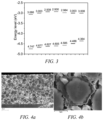
Fig. 3 is an energy level diagram of an interface passivation material according to yet another embodiment of the present application. -
Fig. 4a is an SEM image of a passivation layer according to another embodiment of the present application, andFig. 4b is a partial enlarged view ofFig. 4a . -
Fig. 5 is a plan view of the perovskite solar cell shown inFig. 1 . -
Fig. 6 is a cross-sectional view of the perovskite solar cell shown inFig. 1 . -
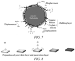
Fig. 7 is a diagram of the passivation principle of a perovskite solar cell according to one embodiment of the present application. -
Fig. 8 is a schematic diagram of the process of the preparation of the perovskite layer and the interface passivation layer in a perovskite solar cell of one embodiment of the present application. - Hereinafter, embodiments of the perovskite solar cell, preparation method therefor, battery module, battery pack and electrical device of the present application are disclosed in detail appropriately with reference to the detailed description of the drawings. However, unnecessary detailed illustrations may be omitted in some instances. For example, there are situations where detailed description of well known items and repeated description of actually identical structures are omitted. This is to prevent the following description from being unnecessarily verbose, and facilitates understanding by those skilled in the art. Moreover, the accompanying drawings and the descriptions below are provided for enabling those skilled in the art to fully understand the present application, rather than limiting the subject matter disclosed in claims.
- "Ranges" disclosed in the present application are defined in the form of lower and upper limits, and a given range is defined by selection of a lower limit and an upper limit, the selected lower and upper limits defining the boundaries of the particular range. Ranges defined in this manner may be inclusive or exclusive, and may be arbitrarily combined, that is, any lower limit may be combined with any upper limit to form a range. For example, if the ranges of 60 to 120 and 80 to 110 are listed for a particular parameter, it should be understood that the ranges of 60 to 110 and 80 to 120 are also contemplated. Additionally, if the minimum range values 1 and 2 are listed, and the maximum range values 3, 4, and 5 are listed, the following ranges are all contemplated: 1-3, 1-4, 1-5, 2-3, 2-4 and 2-5. In the present application, unless otherwise stated, the numerical range "a-b" represents an abbreviated representation of any combination of real numbers between a and b, wherein a and b are both real numbers. For example, the numerical range "0-5" means that all real numbers between "0-5" have been listed herein, and "0-5" is just an abbreviated representation of combinations of these numerical values. In addition, when a parameter is expressed as an integer of ≥ 2, it is equivalent to disclosing that the parameter is, for example, an integer of 2, 3, 4, 5, 6, 7, 8, 9, 10, 11, 12, etc.
- All the embodiments and optional embodiments of the present application can be combined with one another to form new technical solutions, unless otherwise stated.
- All the technical features and optional technical features of the present application can be combined with one another to form a new technical solution, unless otherwise stated.
- The terms "comprise" and "include" mentioned in the present application are open-ended or closed-ended, unless otherwise stated. For example, the terms "include" and "comprise" may mean that other components not listed may also be included or comprised, or only the listed components may be included or comprised.
- In the present application, the term "or" is inclusive unless otherwise specified. For example, the phrase "A or B" means "A, B, or both A and B". In more particular, the condition "A or B" is satisfied by any one of the following: A is true (or present) and B is false (or not present); A is false (or not present) and B is true (or present); or both A and B are true (or present).
- Referring to
Fig. 1 , the perovskite solar cell of the present application can be made up of, in order from top to bottom, a (metal) back electrode, an electron/hole transport layer, a passivation layer, a perovskite layer, a passivation layer, a hole/electron transport layer, and conductive glass. - In the perovskite solar cell of the present application, the surface of the perovskite layer is passivated by an interface passivation material to form an interface passivation layer, wherein the HOMO energy level of an interface between the perovskite layer and the interface passivation layer is 0.01-0.4 eV, and the energy band gap between the HOMO energy level and the LUMO energy level is 0.01-0.4 eV; and the interface passivation material contains: an organic amine salt of a biphenyl compound and/or an organic amine salt of an acene compound.
- Referring to
Fig. 2 , taking FAPbI3 (perovskite layer) and Spiro (hole transport layer) for example, the VBMs of the two are respectively -5.5 and -5.2, and a larger energy level difference leads to a decrease in open circuit voltage. However, the use of the organic amine salts of biphenyl compounds and/or organic amine salts of acene compounds increase the VBM of the perovskite layer, which is beneficial for the extraction of holes and improve the transport efficiency of carriers. - In the present application, the biphenyl compounds include biphenyl, o-terphenyl, m-terphenyl and p-terphenyl, and the structural formulas thereof are as follows: in order from left to right,
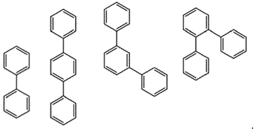
- In the present application, the acene compounds include naphthalene, anthracene, phenanthrene, tetracene and pentacene, and the structural formulas thereof are as follows: in order from left to right,

- Existing interface passivation materials are effective in improving the efficiency and stability of cells to a certain extent. By contrast, it has been found that organic ammonium salts composed of biphenyl compounds and acene compounds more significantly improve the performance and long-term stability of cells.
- In particular, the biphenyl compounds and acene compounds are both compounds with multi-benzene rings. By using multi-benzene rings, the valence band energy level position of the surface of organic hybrid perovskite can be improved, providing more excellent energy level matching with the hole transport layer, which is conducive to carrier transport and improves the cell efficiency. Referring to
Fig. 3 , by using an interface passivation material with a multi-benzene structure to adjust the energy level of perovskite, with the increase of the number of benzene rings, the expanded π conjugated system (or π range) increases the number of coupled molecular orbitals and enhances the degree of π delocalization, so the HOMO energy level increases, while the LUMO energy level changes little. - The energy level detection method involves using ultraviolet photoelectron spectroscopy (UPS). After characterization by a device, the energy level position thereof is calculated by the Fermi edge and cut-off edge thereof. In addition, a UV-Vis spectrophotometer is used to measure the spectral absorption thereof, and the band gap thereof is measured according to formula transformation.
- Furthermore, the introduction of the multi-benzene rings into the biphenyl compounds and acene compounds as electron-donating functional groups can not only improve the bonding energy of the interface passivation material at defect sites, but can also enhance the proton bonding capacity of the interface passivation material itself, thus enhancing the inherent stability thereof.
- In addition, as hydrophobic functional groups, the multi-benzene rings cover the surface of the perovskite layer to form a dense hydrophobic layer, which can improve the water stability of the perovskite layer. Referring to
Figs. 4a and 4b , the passivation layer covering the surface of the perovskite layer is a dense hydrophobic layer, thereby improving the water stability of the perovskite layer. After energy level matching, the extraction of holes is facilitated, and the capacity of the hole transport layer to extract perovskite holes increases. - Referring to
Figs. 5 and 6 , it can also be seen that the passivation layer included in the perovskite solar cell of the present application is dense, such that the water stability of the perovskite layer can be improved. - In summary, in the perovskite solar cell of the present application, the surface of the perovskite layer is passivated by using an interface passivation material containing an organic amine salt of a biphenyl compound and/or an organic amine salt of an acene compound to form an interface passivation layer; in addition, the HOMO energy level of the interface between the perovskite layer and the interface passivation layer is 0.01-0.4 eV, and the energy band gap between the HOMO energy level and the LUMO energy level is 0.01-0.4 eV, that is, after energy level matching, the open circuit voltage of the device increases, and after defect passivation, the carrier recombination decreases, and the current increases; in addition, defect passivation and the anchoring of functional groups to perovskite increase the phase stability of perovskite and make it difficult to decompose, and the multi-benzene structure increases the water stability of the perovskite solar cell and obviously improves the long-term stability thereof.
- In the perovskite solar cell of the present application, the introduction of different electron-donating groups and electron-withdrawing groups to the organic amine salt of biphenyl compound and/or the organic amine salt of acene compound contained in the interface passivation material can regulate the energy level, wherein:
the electron-donating group is one or more selected from a superstrong electron-donating group, a strong electron-donating group, a medium electron-donating group and a weak electron-donating group: - superstrong electron-donating group: oxygen anion (-O-);
- strong electron-donating group: dialkylamino (-NR2), alkylamino (-NHR), amino (-NH2), hydroxyl (-OH), and alkoxy (-OR);
- medium electron-donating group: amide group (-NHCOR) and acyloxy (-OCOR); and
- weak electron-donating group: alkyl (-R), carboxymethyl (-CH2COOH), and phenyl (-Ph),
- wherein the above-mentioned alkyl has a carbon atom number of 1-10.
- In addition, the electron-withdrawing group is one or more selected from a strong electron-withdrawing group, a medium electron-withdrawing group and a weak electron-withdrawing group:
- strong electron-withdrawing group: tertiary amine cation (-N+R3), nitro (-NO2), and trihalomethyl (-CX3), with X = F or Cl;
- medium electron-withdrawing group: cyano (-CN) and sulfonic acid group (-SO3H); and
- weak electron-withdrawing group: formyl (-CHO), acyl (-COR), and carboxyl (-COOH).
- With the increase of the number of benzene rings in the organic amine salts of biphenyl compounds and/or the organic amine salts of acene compounds, the difficulty of synthesis becomes higher and higher, and the larger structure may lead to increased steric hindrance. In this regard, the position of energy level can be adjusted by adding electron-donating and electron-withdrawing groups to the benzene ring. In summary, the electron-donating group can improve the HOMO energy level thereof, while the electron-withdrawing group can reduce the LUMO energy level thereof. By means of cooperation with different groups, the energy level position and band gap thereof can be adjusted. By adjusting the energy level of this molecule, the electronic structure of the perovskite layer surface can be adjusted, and the energy level of the perovskite layer is thus adjusted to make it more match with the energy level of the hole transport layer.
- Furthermore, in the perovskite solar cell of the present application, the organic amine salts of biphenyl compounds and/or the organic amine salts of acene compounds further have one or more selected from sulfonate ion (-SO3H), nitrate ion (NO3 -), acetate ion (CH3COO-), phosphate ion (PO4 3-), fluoride ion (F-), iodide ion (I-), bromide ion (Br-) and chloride ion (Cl-), as an anion.
- The organic amine compounds of biphenyl compounds and acene compounds are prepared into salts, wherein the biphenyl and acene are used as cations; and the anionic moiety is an alkyl acid containing O, S, P, N, F, I, Br or Cl, such as oleic acid or alkyl sulfonic acid, preferably an acid radical ion containing O, S, P, N, Cl, Br or I. On the one hand, the acid radical ion containing O, S, P, N, Cl, Br or I can form hydrogen bond with the A position in perovskite to stabilize the organic cation; on the other hand, some acid radical ions containing O and S can anchor Pb. The interaction can well stabilize the perovskite phase and has a better effect on the long-term stability of the solar cell. More preferably, the acid radical ions are Cl, Br, and I, and organic acid salts with alkyl chains are particularly preferred as anions.
- The anionic moiety is certain for energy level adjustment and interface passivation. If a halogen ion is selected as the anion, the halogen vacancies on the surface of the perovskite layer can be compensated. If an organic acid salt with an alkyl chain is used as the anion, the alkyl chain has the ability to donate electrons, which increases the electronegativity of the anion. On the one hand, the anion can improve the electrostatic interaction with the cation; on the other hand, it can improve the ability to bond with the A and B positions in perovskite so as to stabilize the structure of the perovskite.
- In addition, taking
Fig. 7 for example, the anion affects the passivation effect to a certain extent, and the halogen anion can make up for the defects in the X position, wherein F ion can form a hydrogen bond with the cation in the A position to stabilize the cation in the A position. In addition, oxygen-containing acid radicals (such as acetate ions and phosphate ions) can better chelate Pb ion, and can resist oxidation compared with iodide ion, thus avoiding the formation of elementary iodine, a harmful substance. - A method for preparing the perovskite solar cell of the present application is provided, which comprises, in order, (I) a process of preparing an electron transport layer, (II) a process of preparing a perovskite layer and a passivation layer, (III) a process of preparing a hole transport layer, and (IV) a process of preparing a back electrode, such that the perovskite solar cell of the present application is manufactured, wherein the (II) process of preparing the perovskite layer and the passivation layer comprises
- (1) respectively preparing a perovskite precursor solution and an anti-solvent solution of an interface passivation material;
- (2) on conductive glass spun-coated with the electron transport layer, initially dripping the perovskite precursor solution for spin coating, and then dripping the anti-solvent solution of the interface passivation material for spin coating in a synchronous manner; and
- (3) performing annealing to form the perovskite layer and the passivation layer.
- In process (1), the perovskite precursor is dissolved in a solvent to obtain a perovskite precursor solution, wherein the perovskite precursor comprises: one or more selected from CsBr, FABr, MABr, CsI, FAI, MAI, CsCl, FACl, and MACl; and one or more selected from PbBr2, SnBr2, PbI2, SnI2, PbCl2 and SnCl2, wherein the solvent is one or more selected from DMF, DMSO, NMP and GBL. From the point of view of controlling crystallization, it is preferable that the perovskite precursor comprises: a combination of PbI2 and FAI, a combination of PbI2, FAI and MACl, a combination of MAI and PbI2, and a combination of CsI and PbI2; and from the point of view of controlling crystallization, it is preferable that the solvent is two or more selected from DMF, DMSO, NMP and GBL, for example: a combination of DMF and DMSO, and a combination of DMF and NMP.
- In process (1), the interface passivation material is dissolved in an anti-solvent to obtain an anti-solvent solution of the interface passivation material, wherein from the point of view of interface passivation, the interface passivation material is preferably one or more selected from p-fluorophenylethylamine, naphthyl ethyl amine, anthrylethylamine, 2-methoxynaphthalene ethylamine hydroiodide, and 2-methoxynaphthalene ethylamine acetate, and more preferably one or more selected from naphthylethylamine, anthrylethylamine, and 2-methoxynaphthalene ethylamine hydroiodide. Furthermore, from the point of view of the degree of difficulty in the dissolution of the solvent from the perovskite precursor solution and the solubility of the interface passivation material, it is preferable that the anti-solvent is one selected from toluene, chlorobenzene, dichlorobenzene, ethyl acetate and diethyl ether.
- The process of preparing the perovskite layer involves dripping a perovskite precursor solution to the electron transport layer, initially performing spin coating, then dripping an anti-solvent solution dissolved with an interface passivation material during spin coating, and performing spin coating in a synchronous manner. The anti-solvent can extract the solvent from the perovskite precursor solution, such that the solute crystal precipitates out, which is namely the perovskite layer. Further taking
Fig. 8 for example, the process of preparing the perovskite layer and interface passivation layer involves initially dripping a perovskite precursor solution for spin coating, and after spin coating for a period of time, dripping an anti-solvent solution dissolved with an interface passivation material for spin coating in a synchronous manner, so as to form perovskite and an interface passivation layer at the same time during spin coating. - The interface passivation layer is formed by spin-coating a layer of interface passivation material on the perovskite layer and performing annealing, and it has both the passivation and interface control functions, thus achieving a higher photoelectric conversion efficiency and stability.
- From the point of view of the solubility, the dissolution of perovskite, and the difficulty for the solvent, in the anti-solvent solution of the interface passivation material, one or more selected from benzene, anhydrous ethanol, isopropanol, butanol, chloroform, methyl butyrate, anisole, xylene and trimethylbenzene is further added as an additional solvent. Therefore, on the premise of not affecting the perovskite layer, the solvent of the perovskite precursor solution can be well extracted, and the perovskite can be well crystallized.
- In addition, in the anti-solvent solution of the interface passivation material, the concentration of the interface passivation material is 0.1-40 mmol/L, and from the point of view of the passivation of the perovskite layer interface, it is preferably 0.5-2 mmol/L, more preferably 0.5-1 mmol/L.
- In addition, in process (2), the spin coating period for the perovskite precursor solution is 10-120 seconds. From the point of view of obtaining an excellent perovskite layer, the spin coating period is preferably 10-40 seconds, more preferably 15-30 seconds.
- In addition, in process (2), during the process of spin coating with the perovskite precursor solution, the anti-solvent solution of the interface passivation material is dripped. For example, if the spin coating period for the perovskite precursor solution is 45 seconds, then the perovskite precursor solution is dripped in one step at the 0th second of the whole period, only the perovskite precursor solution is then initially spun-coated at the 0-25th seconds, the anti-solvent solution of the interface passivation material is dripped at the 25th second, and the perovskite precursor solution and the anti-solvent solution of the interface passivation material are simultaneously spun-coated at the 25-45th second.
- The passivation material is added to an anti-solvent. The thickness of the passivation layer formed on the perovskite surface can be controlled by the concentration and the spin coating period, which can reduce the tedious process of preparing the passivation layer and avoid the influence of multiple annealing on the thin film. Therefore, passivation can be realized during perovskite crystallization. In this regard, the passivation material can better bond with perovskite at the grain boundary and interface to stabilize the perovskite phase, the grain boundary and surface can be passivated at the same time, and the carriers can be prevented from recombination at the grain boundary and interface. If the grain boundary is relatively small, it will be difficult for conventional interface passivation materials to penetrate deep into the grain boundary, and the passivation effect is not good, so it is difficult to completely passivate the defects. In the present application, it is added when the perovskite phase is unstable, which makes it easier to make up for the defects in various positions.
- In process (3), the annealing temperature is 100-200°C, and the annealing time is 10-120 min. In addition, before the annealing in process (3), pre-annealing is optionally performed, wherein the pre-annealing temperature is 60-150°C, and the pre-annealing time is 30 min or less. In the present application, annealing can be performed only once, or alternatively, pre-annealing is performed once before annealing, which avoids multiple annealing of perovskite in the prior art, saves time and cost, and improves the cell manufacturing efficiency.
- In addition, in the method for preparing the perovskite solar cell of the present application, in the (I) process of preparing the electron transport layer, the electron transport layer material solution is spun-coated on the surface of the conductive glass and then annealed to obtain the electron transport layer; in the (III) process of preparing the hole transport layer, the hole transport layer material solution is spun-coated on the surface of the perovskite layer and the passivation layer to obtain the hole transport layer; and in the (IV) process of preparing the back electrode, an electrode position is scraped and evaporated with silver to obtain the back electrode. By means of the above-mentioned processes (I) - (IV), the perovskite solar cell of the present application is obtained.
- In addition, the present application further provides a power consuming device, comprising the perovskite solar cell provided by the present application. The perovskite solar cell can be used as a power supply for the power consuming device, or can also be used as an energy storage unit for the power consuming device. The power consuming device can include (1) user solar power supplies: small-sized power supplies ranging from 10 to 100 W used in remote areas without electricity, such as plateaus, islands, pastoral areas, and border guard posts, for military and civilian living electricity, e.g. lighting, television, and radio-cassette recorder, 3-5 KW home roof grid-connected power generation systems, and photovoltaic water pumps that solve the problems of drinking and irrigation by deep wells in areas without electricity; (2) transportation field: for example, beacon lights, traffic/railway signal lights, traffic warning/sign lights, street lights, high-altitude obstacle lights, radio telephone booths on highways/railways, unattended road shift power supplies, etc.; (3) communication/correspondence field: unattended solar microwave relay stations, optical cable maintenance stations, broadcasting/communication/paging power systems; rural carrier telephone photovoltaic systems, small communication machines, GPS power supplies for soldiers, etc.; (4) petroleum, marine and meteorological fields: solar power supply systems for cathodic protection of petroleum oil pipelines and water reservoir gates, living and emergency power supplies for petroleum oil drilling platforms, marine detection equipment, meteorological/hydrological observation equipment, etc.; (5) power supplies for household lamps: yard lights, street lights, hand lamps, camping lights, mountaineering lights, fishing lights, black light lamps, rubber tapping lights, energy-saving lamps, etc.; (6) photovoltaic power stations: 10 KW-50 MW independent photovoltaic power stations, wind-solar (diesel) complementary power stations, charging stations for various large parking lots, etc.; and (7) solar buildings: those that combine solar power generations with building materials to make future large-scale buildings self-sufficient in electricity, without limitation thereto.
- Hereinafter, the examples of the present application will be explained. The examples described below are exemplary and are merely for explaining the present application, and should not be construed as limiting the present application. The examples in which no techniques or conditions are specified are based on the techniques or conditions described in documents in the art or according to product introductions. The reagents or instruments used therein for which no manufacturers are specified are all conventional products that are commercially available.
- The method for preparing a perovskite solar cell according to Example 1 involved initially treating conductive glass according to a conventional method, and then performing, in order, (I) the preparation of an electron transport layer, (II) the preparation of a perovskite layer and a passivation layer, (III) the preparation of a hole transport layer, and (IV) the preparation of a back electrode, such that the perovskite solar cell according to Example 1 was manufactured. In particular,
- 20 pieces of FTO conductive glass with a size of 2.0 * 2.0 cm were taken, and 0.35 cm FTO was removed at both ends by laser etching to expose a glass substrate.
- The etched FTO conductive glass was ultrasonically cleaned several times with water, acetone and isopropanol in order.
- The FTO conductive glass was blown with a nitrogen gun to dry off the solvent and put into an ultraviolet ozone machine for further cleaning.
- A 30% tin oxide colloid was mixed with deionized water at a ratio of 1 : 3 to form a 10 mg/mL tin oxide colloid aqueous solution, the aqueous solution was stirred at room temperature for 1 h, and 70 µL was taken as an electron transport layer solution, spun-coated on the surface of the FTO conductive glass treated with ultraviolet and ozone at a speed of 4000 rpm/s, heated at 150°C for 15 min, and annealed on a stage at 150°C for 15 min to obtain an electron transport layer.
- In addition, the compounding proportion of the tin oxide colloid aqueous solution could be adjusted within the range of 30% tin oxide colloid : water = 1 : 1-5.
- As shown in Table 1, a perovskite precursor solution was prepared, magnetically stirred at room temperature for 1 h, and filtered for later use. In addition, the interface passivation material was dissolved in an anti-solvent to obtain an anti-solvent solution of the interface passivation material, whereby a perovskite precursor solution and an anti-solvent solution of the interface passivation material were respectively prepared. The above-mentioned FTO conductive glass spun-coated with the electron transport layer was irradiated with UV for 15 min, 60 µL of the perovskite precursor solution was initially dripped on the FTO conductive glass for spin coating; and as shown in Table 1, after spin coating for a period of time, 600 µL of the anti-solvent solution of the interface passivation material was dripped for spin coating in a synchronous manner, followed by annealing at 150°C for 1 h.
- Alternatively, pre-annealing could be performed prior to annealing.
- Li-TFSI, tBP and FK209 were added to spiro, stirred for 1 h, filtered and used as a hole transport layer material solution for later use, 60 µL of spiro was dripped on the above-mentioned conductive glass spun-coated with the perovskite layer and the passivation layer, and the hole transport layer material solution was spun-coated to obtain a hole transport layer.
- An electrode position was scraped on the above-mentioned cell spun-coated with the hole transport layer, the residual functional layer was wiped off with a washing liquid, and the cell was placed in an evaporation Mask and evaporated with 80 nm silver in a vacuum evaporation device to obtain the perovskite solar cell of the present application.
- In Examples 2-20, perovskite solar cells were prepared by the same method as in Example 1, except that as shown in Table 1, the following were changed: the perovskite precursor material, the solvent for dissolving the perovskite precursor, the spin coating period for the perovskite precursor solution, the interface passivation material, the anti-solvent, the concentration of the interface passivation material in the anti-solvent, the dripping timing for the anti-solvent solution of the interface passivation material, the optional pre-annealing temperature and time, and the annealing temperature and time.
- In Comparative Example 1, a perovskite solar cell was prepared by the same method as in Example 1, except that no interface passivation material was added to the anti-solvent.
- In Comparative Example 2, a perovskite solar cell was prepared by the same method as in Example 5, except that the interface passivation material was butylamine iodide.
- The perovskite solar cells obtained in Examples 1-20 and Comparative Examples 1 and 2 were tested below for cell efficiency, and the results were altogether shown in Table 1.
- Spectrum: AM 1.5G spectrum; Light intensity: 1000 W/m2; Room temperature 25°C.
- The solar cell was connected to positive and negative electrodes of a digital source meter, respectively, and the photoelectric conversion efficiency thereof was measured.
Table 1 Experiment item Perovskite layer Passivation layer Pre-annealing Annealing Cell efficiency Perovskite precursor Solvent Spin coating period Interface passivation material Anti-solvent Concentration (mmol/L) Dripping timing Temperature Time Temperature Time Example 1 Combinatio n of FAI and PbI2 Combination of DMF and NMP 45 seconds (wherein only the perovskite precursor solution was spun-coated at the 0-25th second) p-Fluorophenethyl amine Chloroben zene 0.5 At the 25th second during the spin-coating of the perovskite precursor solution, the anti-solvent solution of the interface passivation material was dripped, and they were then spun-coated in a synchronous manner from the 25th to 45th seconds in the whole spin-coating period. - - 150°C 60 min 22.32 Example 2 Combinatio n of FAI and PbI2 Combination of DMF and NMP 45 seconds (wherein only the perovskite precursor solution was spun-coated at the 0-25th second) p-Fluorophenethyl amine Toluene 0.5 At the 25th second during the spin-coating of the perovskite precursor solution, the anti-solvent solution of the interface passivation material was dripped, and they were then spun-coated in a synchronous manner from the 25th to 45th seconds in the whole spin-coating period. - - 150°C 60 min 22.12 Example 3 Combinatio n of FAI and PbI2 Combination of DMF and NMP 45 seconds (wherein only the perovskite precursor p-Fluorophenethyl amine Chloroben zene 1 At the 25th second during the spin-coating of the perovskite precursor - - 150°C 60 min 22.82 solution was spun-coated at the 0-25th second) solution, the anti-solvent solution of the interface passivation material was dripped, and they were then spun-coated in a synchronous manner from the 25th to 45th seconds in the whole spin-coating period. Example 4 Combinatio n of FAI and PbI2 Combination of DMF and NMP 45 seconds (wherein only the perovskite precursor solution was spun-coated at the 0-25th second) p-Fluorophenethyl amine Chloroben zene 2 At the 25th second during the spin-coating of the perovskite precursor solution, the anti-solvent solution of the interface passivation material was dripped, and they were then spun-coated in a synchronous manner from the 25th to 45th seconds in the whole spin-coating period. - - 150°C 60 min 22.10 Example 5 Combinatio n of FAI, PbI2 and MAC1 Combination of DMF and DMSO 120 seconds (wherein only the perovskite precursor solution was spun-coated at the 0-70th second) Naphthylethyla mine Chloroben zene 0.5 At the 70th second during the spin-coating of the perovskite precursor solution, the anti-solvent solution of the interface passivation material was dripped, and they were then spun-coated in a synchronous manner from the 70th to 120th seconds in the whole spin-coating period. 100°C 30 min 200°C 120 min 23.88 Example 6 Combinatio n of FAI, PbI2 and MAC1 Combination of DMF and DMSO 120 seconds (wherein only the perovskite precursor solution was spun-coated at the 0-70th second) Naphthylethyla mine Ethyl acetate 0.5 At the 70th second during the spin-coating of the perovskite precursor solution, the anti-solvent solution of the interface passivation material was dripped, and they were then spun-coated in a synchronous manner from the 70th to 120th seconds in the whole spin-coating period. 100°C 30 min 200°C 120 min 23.65 Example 7 Combinatio n of FAI, PbI2 and MAC1 Combination of DMF and DMSO 120 seconds (wherein only the perovskite precursor solution was spun-coated at the 0-70th second) Naphthylethyla mine Chloroben zene 1 At the 70th second during the spin-coating of the perovskite precursor solution, the anti-solvent solution of the interface passivation material was dripped, and they were then spun-coated in a synchronous manner from the 70th to 120th seconds in the whole spin-coating period. 100°C 30 min 200°C 120 min 24.09 Example 8 Combinatio n of FAI, PbI2 and MAC1 Combination of DMF and DMSO 120 seconds (wherein only the perovskite precursor solution was spun-coated at the 0-70th second) Naphthylethyla mine Chloroben zene 2 At the 70th second during the spin-coating of the perovskite precursor solution, the anti-solvent solution of the interface passivation material was dripped, and they were then spun-coated in a synchronous manner from the 70th to 120th seconds in the whole spin-coating period. 100°C 30 min 200°C 120 min 23.53 Example 9 Combinatio n of FAI, PbI2 and MACl Combination of DMF and DMSO 120 seconds (wherein only the perovskite precursor solution was spun-coated at the 0-70th second) Anthrylethylami ne Chloroben zene 0.5 At the 70th second during the spin-coating of the perovskite precursor solution, the anti-solvent solution of the interface passivation material was dripped, and they were then spun-coated in a synchronous manner from the 70th to 120th seconds in the whole spin-coating period. 100°C 30 min 200°C 120 min 22.65 Example 10 Combinatio n of FAI, PbI2 and MACl Combination of DMF and DMSO 120 seconds (wherein only the perovskite precursor solution was spun-coated at the 0-70th second) Anthrylethylami ne Ethyl acetate 0.5 At the 70th second during the spin-coating of the perovskite precursor solution, the anti-solvent solution of the interface passivation material was dripped, and they were then spun-coated in a synchronous manner from the 70th to 120th seconds in the whole spin-coating period. 100°C 30 min 200°C 120 min 22.42 Example 11 Combinatio n of FAI, PbI2 and MAC1 Combination of DMF and DMSO 120 seconds (wherein only the perovskite precursor solution was spun-coated at the 0-70th second) Anthrylethylami ne Chloroben zene 1 At the 70th second during the spin-coating of the perovskite precursor solution, the anti-solvent solution of the interface passivation material was dripped, and they were then spun-coated in a synchronous manner from the 70th to 120th seconds in the whole spin-coating period. 100°C 30 min 200°C 120 min 23.62 Example 12 Combinatio n of FAI, PbI2 and MAC1 Combination of DMF and DMSO 120 seconds (wherein only the perovskite precursor solution was spun-coated at the 0-70th second) Anthrylethylami ne Chloroben zene 2 At the 70th second during the spin-coating of the perovskite precursor solution, the anti-solvent solution of the interface passivation material was dripped, and they were then spun-coated in a synchronous manner from the 70th to 120th seconds in the whole spin-coating period. 100°C 30 min 200°C 120 min 22.12 Example 13 Combinatio n of GBL and NMP Combination of GBL and NMP 90 seconds (wherein only the perovskite precursor solution was spun-coated at the 0-50th second) 2-Methoxynaphth alene ethylamine hydroiodide Chloroben zene 0.5 At the 50th second during the spin-coating of the perovskite precursor solution, the anti-solvent solution of the interface passivation material was dripped, and they were then spun-coated in a synchronous manner from the 50th to 90th seconds in the whole spin-coating period. 70° C 15 min 150°C 90 min 23.88 Example 14 Combinatio n of GBL and NMP Combination of GBL and NMP 90 seconds (wherein only the perovskite precursor solution was spun-coated at the 0-50th second) 2-Methoxynaphth alene ethylamine hydroiodide Diethyl ether 0.5 At the 50th second during the spin-coating of the perovskite precursor solution, the anti-solvent solution of the interface passivation material was dripped, and they were then spun-coated in a synchronous manner from the 50th to 90th seconds in the whole spin-coating period. 70° C 15 min 150°C 90 min 24.03 Example 15 Combinatio n of GBL and NMP Combination of GBL and NMP 90 seconds (wherein only the perovskite precursor solution was spun-coated at the 0-50th second) 2-Methoxynaphth alene ethylamine hydroiodide Chloroben zene 1 At the 50th second during the spin-coating of the perovskite precursor solution, the anti-solvent solution of the interface passivation material was dripped, and they were then spun-coated in a synchronous manner from the 50th to 90th seconds in the whole spin-coating period. 70° C 15 min 150°C 90 min 24.32 Example 16 Combinatio n of GBL and NMP Combination of GBL and NMP 90 seconds (wherein only the perovskite precursor solution was spun-coated at the 0-50th second) 2-Methoxynaphth alene ethylamine hydroiodide Chloroben zene 2 At the 50th second during the spin-coating of the perovskite precursor solution, the anti-solvent solution of the interface passivation material was dripped, and they were then spun-coated in a synchronous manner from the 50th to 90th seconds in the whole spin-coating period. 70° C 15 min 150°C 90 min 23.01 Example 17 Combinatio n of CsI, SnBr2 and SnI2 GBL 10 seconds (wherein only the perovskite precursor solution was spun-coated at the 0-5th second) 2-Methoxynaphth alene ethylamine acetate Chloroben zene 1 At the 5th second during the spin-coating of the perovskite precursor solution, the anti-solvent solution of the interface passivation material was dripped, and they were then spun-coated in a synchronous manner from the 5th to 10th seconds in the whole spin-coating period. 40°C 5 min 100° C 10 min 10.32 Example 18 Combinatio n of CsI and PbI2 DMF 45 seconds (wherein only the perovskite precursor solution was spun-coated at the 0-25th second) p-Fluorophenethyl amine Chloroben zene 0.1 At the 25th second during the spin-coating of the perovskite precursor solution, the anti-solvent solution of the interface passivation material was dripped, and they were then spun-coated in a synchronous manner from the 25th to 45th seconds in the whole spin-coating period. - - 150°C 60 min 20.63 Example 19 Combinatio n of CsI and PbI2 DMF 45 seconds (wherein only the perovskite precursor solution was spun-coated at the 0-25th second) p-Fluorophenethyl amine Chloroben zene 20 At the 25th second during the spin-coating of the perovskite precursor solution, the anti-solvent solution of the interface passivation material was dripped, and they were then spun-coated in a synchronous manner from the 25th to 45th seconds in the whole spin-coating period. - - 150°C 60 min 23.46 Example 20 Combinatio n of CsI and PbI2 DMF 45 seconds (wherein only the perovskite precursor solution was spun-coated at the 0-25th second) p-Fluorophenethyl amine Chloroben zene 40 At the 25th second during the spin-coating of the perovskite precursor solution, the anti-solvent solution of the interface passivation material was dripped, and they were then spun-coated in a synchronous manner from the 25th to 45th seconds in the whole spin-coating period. - - 150°C 60 min 22.02 Comparativ e Example 1 Combinatio n of FAI and PbI2 Combination of DMF and NMP 45 seconds (wherein only the perovskite precursor solution was spun-coated at the 0-25th second) Chloroben zene At the 25th second during the spin-coating of the perovskite precursor solution, the anti-solvent was dripped, and they were then spun-coated in a synchronous manner from the 25th to 45th seconds in the whole spin-coating period. - - 150°C 60 min 19.52 Comparativ e Example 2 Combinatio n of FAI, PbI2 and MAC1 Combination of DMF and DMSO 120 seconds (wherein only the perovskite precursor solution was spun-coated at the 0-70th second) Butylamine iodide Chloroben zene 0.5 At the 70th second during the spin-coating of the perovskite precursor solution, the anti-solvent solution of the interface passivation material was dripped, and they were then spun-coated in a synchronous manner from the 70th to 120th seconds in the whole spin-coating period. 100°C 30 min 200°C 120 min 20.03 - As could be seen from Table 1:
In Examples 1-20, in the preparation of the perovskite solar cells, as for the preparation process of the perovskite layer and passivation layer, the perovskite precursor solution was initially dripped; and after spin coating for a period of time, the anti-solvent solution dissolved with the interface passivation material was then dripped, and after annealing, the perovskite layer and the passivation layer were obtained. The two layers were obtained at one time, which avoided secondary annealing. - From Examples 1-20, it could be seen that in the perovskite solar cell of the present application, the cell efficiency could be greatly improved by using the specific perovskite precursor material, the specific solvent, the specific interface passivation material, the specific anti-solvent, the control of the concentration of the interface passivation material in the anti-solvent, the specific spin-coating period for the perovskite precursor solution, the specific dripping timing for the anti-solvent solution of the interface passivation material, the optional pre-annealing temperature and time, and the annealing temperature and time all within the specific ranges.
- In Comparative Example 1, during the preparation of the perovskite solar cell, the perovskite precursor solution was initially dripped; and after spin coating for a period of time, the anti-solvent was dripped, which was pure chlorobenzene free of interface passivation material, and after annealing, the perovskite layer was obtained while no passivation layer was formed. In Comparative Example 2, during the preparation of the perovskite solar cell, the perovskite precursor solution was initially dripped; and after spin coating for a period of time, the anti-solvent was dripped, and after annealing, the perovskite layer was obtained while the passivation layer was formed, wherein the anti-solvent was pure chlorobenzene, and the interface passivation material was butylamine iodide. Compared with Examples 1-20, the cell efficiency was low.
- It should be noted that the present application is not limited to the above embodiments. The above embodiments are exemplary only, and any embodiment that has substantially same constitutions as the technical ideas and has the same effects within the scope of the technical solution of the present application falls within the technical scope of the present application. In addition, without departing from the gist of the present application, various modifications that can be conceived by those skilled in the art to the embodiments, and other modes constructed by combining some of the constituent elements of the embodiments also fall within the scope of the present application.
Claims (11)
- A perovskite solar cell, whereinthe perovskite solar cell has, in order, a back electrode, a hole transport layer, an interface passivation layer, a perovskite layer, an interface passivation layer, an electron transport layer, and conductive glass,wherein the HOMO energy level of an interface between the perovskite layer and the interface passivation layer is 0.01-0.4 eV, and the energy band gap between the HOMO energy level and the LUMO energy level is 0.01-0.4 eV; andthe interface passivation layer contains: an organic amine salt of a biphenyl compound and/or an organic amine salt of an acene compound.
- The perovskite solar cell according to claim 1, wherein
the organic amine salt of the biphenyl compound has one or more selected from biphenyl, o-terphenyl, m-terphenyl and p-terphenyl, as a parent nucleus. - The perovskite solar cell according to claim 2, wherein
the organic amine salt of the acene compound has one or more selected from naphthalene, anthracene, phenanthrene, tetracene and pentacene, as a parent nucleus. - The perovskite solar cell according to any one of claims 1-3, whereinthe organic amine salt of the biphenyl compound and/or the organic amine salt of the acene compound further has an electron-donating group, an electron-withdrawing group and an alkylamine, whereinthe electron-donating group is one or more selected from a superstrong electron-donating group, a strong electron-donating group, a medium electron-donating group and a weak electron-donating group, whereinthe superstrong electron-donating group is oxo,the strong electron-donating group is dialkylamino, alkylamino, amino, hydroxyl or alkoxy, wherein the alkyl has a carbon atom number of 1-10,the medium electron-donating group is an amide group or acyloxy, andthe weak electron-donating group is alkyl, carboxymethyl, or phenyl; andthe electron-withdrawing group is one or more selected from a strong electron-withdrawing group, a medium electron-withdrawing group and a weak electron-withdrawing group, whereinthe strong electron-withdrawing group is tertiary amino, nitro or trihalomethyl,the medium electron-withdrawing group is cyano or a sulfonic acid group, andthe weak electron-withdrawing group is acyl or carboxyl.
- The perovskite solar cell according to any one of claims 1-3, wherein
the organic amine salt of the biphenyl compound and/or the organic amine salt of the acene compound further has one or more selected from sulfonate ion, nitrate ion, acetate ion, phosphate ion, fluoride ion, iodide ion, bromide ion and chloride ion, as an anion. - A method for preparing a perovskite solar cell, whereinthe method for preparing a perovskite solar cell comprises, in order, (I) a process of preparing an electron transport layer, (II) a process of preparing a perovskite layer and a passivation layer, (III) a process of preparing a hole transport layer, and (IV) a process of preparing a back electrode, such that the perovskite solar cell according to any one of claims 1-5 is prepared,wherein the (II) process of preparing the perovskite layer and the passivation layer comprises(1) respectively preparing a perovskite precursor solution and an anti-solvent solution of an interface passivation material;(2) on conductive glass spun-coated with the electron transport layer, initially dripping the perovskite precursor solution for spin coating, and then dripping the anti-solvent solution of the interface passivation material for spin coating in a synchronous manner; and(3) performing annealing to form the perovskite layer and the passivation layer.
- The method for preparing a perovskite solar cell according to claim 6, wherein
in the anti-solvent solution of the interface passivation material, the concentration of the interface passivation material is 0.1-40 mmol/L. - The method for preparing a perovskite solar cell according to claim 6, wherein
in process (2), the spin coating period for the perovskite precursor solution is 10-120 seconds. - The method for preparing a perovskite solar cell according to any one of claims 6-8, wherein
in process (3), the annealing temperature is 100-200°C, and the annealing time is 10-120 min. - The method for preparing a perovskite solar cell according to claim 9, wherein
before the annealing in process (3), pre-annealing is optionally performed, wherein the pre-annealing temperature is 60-150°C, and the pre-annealing time is 30 min or less. - A power consuming device, wherein
the power consuming device has the perovskite solar cell according to any one of claims 1-5, and the perovskite solar cell is used as a power source or energy storage unit of the power consuming device.
Applications Claiming Priority (1)
| Application Number | Priority Date | Filing Date | Title |
|---|---|---|---|
| PCT/CN2021/143771 WO2023123390A1 (en) | 2021-12-31 | 2021-12-31 | Perovskite solar cell and preparation method therefor and electric device |
Publications (2)
| Publication Number | Publication Date |
|---|---|
| EP4231803A1 true EP4231803A1 (en) | 2023-08-23 |
| EP4231803A4 EP4231803A4 (en) | 2023-12-27 |
Family
ID=86997247
Family Applications (1)
| Application Number | Title | Priority Date | Filing Date |
|---|---|---|---|
| EP21960111.9A Pending EP4231803A4 (en) | 2021-12-31 | 2021-12-31 | PEROWSKIT SOLAR CELL AND PRODUCTION METHOD THEREOF AND ELECTRICAL DEVICE |
Country Status (4)
| Country | Link |
|---|---|
| US (1) | US12402467B2 (en) |
| EP (1) | EP4231803A4 (en) |
| CN (1) | CN116918480A (en) |
| WO (1) | WO2023123390A1 (en) |
Cited By (1)
| Publication number | Priority date | Publication date | Assignee | Title |
|---|---|---|---|---|
| CN117153897A (en) * | 2023-08-31 | 2023-12-01 | 环晟光伏(江苏)有限公司 | A solar cell with a passivation layer at the cutting edge and a preparation method thereof |
Families Citing this family (11)
| Publication number | Priority date | Publication date | Assignee | Title |
|---|---|---|---|---|
| CN117202749B (en) * | 2023-09-08 | 2025-05-02 | 大连理工大学 | A type of ethylaminethiourea passivated perovskite film and preparation method thereof and perovskite solar cell |
| CN117580383A (en) * | 2023-12-28 | 2024-02-20 | 通威太阳能(成都)有限公司 | A perovskite solar cell and its preparation method |
| CN120614931A (en) * | 2024-03-08 | 2025-09-09 | 宁德时代新能源科技股份有限公司 | Perovskite solar cell, preparation method, photovoltaic system, power generation device and power consumption device |
| CN120730884A (en) * | 2024-03-27 | 2025-09-30 | 宁德时代未来能源(上海)研究院有限公司 | Solar cell and preparation method thereof, photovoltaic module, power generation device and power consumption device |
| CN118785732B (en) * | 2024-09-11 | 2024-12-20 | 正泰新能科技股份有限公司 | Perovskite solar cell and preparation method thereof |
| CN119300615B (en) * | 2024-10-11 | 2025-10-28 | 浙江大学宁波“五位一体”校区教育发展中心 | Perovskite solar cell and preparation method thereof |
| CN119384196B (en) * | 2024-10-21 | 2025-10-14 | 云南大学 | A method and application of using fluoroaniline/difluoroaniline molecules to improve the performance of perovskite solar cells |
| CN119300618B (en) * | 2024-10-21 | 2025-06-20 | 江苏盛开新能科技有限公司 | Perovskite solar cell, preparation method and prepared laminated perovskite solar cell |
| CN119677308B (en) * | 2024-12-05 | 2025-10-28 | 电子科技大学 | A flexible tin-lead perovskite solar cell and its preparation method |
| CN119816167B (en) * | 2025-01-07 | 2026-01-27 | 河南省科学院材料研究所 | Method for improving illumination stability of perovskite solar cell |
| CN121057413B (en) * | 2025-10-30 | 2026-02-06 | 广东工业大学 | A perovskite solar cell based on a cross-linked interface passivation layer |
Family Cites Families (9)
| Publication number | Priority date | Publication date | Assignee | Title |
|---|---|---|---|---|
| EP2846371A1 (en) * | 2013-09-10 | 2015-03-11 | Ecole Polytechnique Fédérale de Lausanne (EPFL) | Inverted solar cell and process for producing the same |
| PL3084854T3 (en) | 2013-12-17 | 2020-07-13 | Oxford University Innovation Limited | Photovoltaic device comprising a metal halide perovskite and a passivating agent |
| CN110635039B (en) | 2019-08-21 | 2021-01-26 | 厦门大学 | A method of passivating perovskite and perovskite solar cell |
| US20210159022A1 (en) * | 2019-11-26 | 2021-05-27 | Hunt Perovskite Technologies, L.L.C. | 2d perovskite tandem photovoltaic devices |
| CN112864325B (en) * | 2019-11-26 | 2024-03-29 | 中国石油大学(华东) | Method for passivating perovskite film on surface of multifunctional triphenylamine molecule |
| CN111540808B (en) * | 2020-04-03 | 2021-10-15 | 华南师范大学 | A method for preparing high-efficiency carbon electrode inorganic perovskite solar cells from tetrabromoaniline |
| CN115362563A (en) * | 2020-05-28 | 2022-11-18 | 国立研究开发法人科学技术振兴机构 | Film and method for manufacturing the same, circularly polarized light detecting element, circularly polarized light detecting device, and circularly polarized light detecting method |
| CN113809246B (en) * | 2020-06-15 | 2024-06-11 | Tcl科技集团股份有限公司 | Composite material and preparation method thereof and quantum dot light emitting diode |
| CN113363390A (en) * | 2021-06-25 | 2021-09-07 | 南开大学 | High-efficiency perovskite solar cell and preparation method |
-
2021
- 2021-12-31 EP EP21960111.9A patent/EP4231803A4/en active Pending
- 2021-12-31 WO PCT/CN2021/143771 patent/WO2023123390A1/en not_active Ceased
- 2021-12-31 CN CN202180094106.0A patent/CN116918480A/en active Pending
-
2023
- 2023-05-08 US US18/313,394 patent/US12402467B2/en active Active
Cited By (1)
| Publication number | Priority date | Publication date | Assignee | Title |
|---|---|---|---|---|
| CN117153897A (en) * | 2023-08-31 | 2023-12-01 | 环晟光伏(江苏)有限公司 | A solar cell with a passivation layer at the cutting edge and a preparation method thereof |
Also Published As
| Publication number | Publication date |
|---|---|
| WO2023123390A1 (en) | 2023-07-06 |
| US20230320109A1 (en) | 2023-10-05 |
| US12402467B2 (en) | 2025-08-26 |
| EP4231803A4 (en) | 2023-12-27 |
| CN116918480A (en) | 2023-10-20 |
Similar Documents
| Publication | Publication Date | Title |
|---|---|---|
| US12402467B2 (en) | Perovskite solar cell, preparation method therefor and power consuming device | |
| Li et al. | PbCl2-tuned inorganic cubic CsPbBr3 (Cl) perovskite solar cells with enhanced electron lifetime, diffusion length and photovoltaic performance | |
| Krüger et al. | High efficiency solid-state photovoltaic device due to inhibition of interface charge recombination | |
| Kim et al. | Beneficial Effects of PbI 2 Incorporated in Organo-Lead Halide Perovskite Solar Cells. | |
| Adhikari et al. | Crystallization of a perovskite film for higher performance solar cells by controlling water concentration in methyl ammonium iodide precursor solution | |
| Zhao et al. | CH3NH3Cl-assisted one-step solution growth of CH3NH3PbI3: structure, charge-carrier dynamics, and photovoltaic properties of perovskite solar cells | |
| US7943848B2 (en) | Photoelectric conversion element, method of manufacturing the same and solar cell | |
| CN108389967A (en) | The extinction layer material of solar cell, broad-band gap perovskite solar cell and preparation method thereof | |
| CN110483745A (en) | A kind of amphipathic conjugated polymer and its preparing the application in reversed perovskite solar battery | |
| Wang et al. | Full-scale chemical and field-effect passivation: 21.52% efficiency of stable MAPbI3 solar cells via benzenamine modification | |
| CN119300618B (en) | Perovskite solar cell, preparation method and prepared laminated perovskite solar cell | |
| Zhang et al. | Magnesium acetate additive enables efficient and stable carbon electrode based CsPbI2Br perovskite solar cells | |
| CN117999864A (en) | Perovskite solar cell and method of manufacture | |
| CN109585661A (en) | A kind of preparation method of the enhanced bloom in interface-thermostabilization perovskite thin film | |
| Jin et al. | Rhodamine B as an efficient multifunctional passivator for the improvement of perovskite solar cell performance | |
| Liu et al. | Simultaneous improvement in efficiency and photostability of organic solar cells by modifying the ZnO electron-transport layer with curcumin | |
| CN111261786B (en) | Efficient organic solar cell based on asymmetric end-capped electron acceptor | |
| Li et al. | In-situ polymerization of natural amino acids in SnO2 for environmentally friendly and high-efficiency perovskite solar cells | |
| EP4586792A1 (en) | Fullerene composite material and preparation method therefor, perovskite solar cell and preparation method therefor, and electric device | |
| CN113087636A (en) | Iodide and preparation method thereof, and all-inorganic perovskite solar cell based on iodide and preparation method thereof | |
| Ye et al. | Bipyridine type Co-complexes as hole-transporting material dopants in perovskite solar cells | |
| CN114284442B (en) | A high-efficiency perovskite solar cell and its preparation method | |
| CN109851571A (en) | Conjugated organic small molecule interface modification material, preparation method and organic solar cell composed thereof | |
| CN109786565B (en) | Inorganic perovskite solar cell without hole transport layer and preparation method thereof | |
| CN114853763B (en) | D-pi-A compound and application thereof in passivation of perovskite solar cell |
Legal Events
| Date | Code | Title | Description |
|---|---|---|---|
| STAA | Information on the status of an ep patent application or granted ep patent |
Free format text: STATUS: UNKNOWN |
|
| STAA | Information on the status of an ep patent application or granted ep patent |
Free format text: STATUS: THE INTERNATIONAL PUBLICATION HAS BEEN MADE |
|
| PUAI | Public reference made under article 153(3) epc to a published international application that has entered the european phase |
Free format text: ORIGINAL CODE: 0009012 |
|
| STAA | Information on the status of an ep patent application or granted ep patent |
Free format text: STATUS: REQUEST FOR EXAMINATION WAS MADE |
|
| 17P | Request for examination filed |
Effective date: 20230428 |
|
| AK | Designated contracting states |
Kind code of ref document: A1 Designated state(s): AL AT BE BG CH CY CZ DE DK EE ES FI FR GB GR HR HU IE IS IT LI LT LU LV MC MK MT NL NO PL PT RO RS SE SI SK SM TR |
|
| REG | Reference to a national code |
Ref country code: DE Ref legal event code: R079 Free format text: PREVIOUS MAIN CLASS: H10K0030000000 Ipc: H10K0030400000 |
|
| A4 | Supplementary search report drawn up and despatched |
Effective date: 20231124 |
|
| RIC1 | Information provided on ipc code assigned before grant |
Ipc: H10K 85/50 20230101ALI20231120BHEP Ipc: H10K 30/40 20230101AFI20231120BHEP |
|
| RAP1 | Party data changed (applicant data changed or rights of an application transferred) |
Owner name: CONTEMPORARY AMPEREX TECHNOLOGY(HONG KONG) LIMITED |
|
| DAV | Request for validation of the european patent (deleted) | ||
| DAX | Request for extension of the european patent (deleted) | ||
| STAA | Information on the status of an ep patent application or granted ep patent |
Free format text: STATUS: EXAMINATION IS IN PROGRESS |
|
| 17Q | First examination report despatched |
Effective date: 20250704 |